memory hierarchy - electrical and computer...
TRANSCRIPT

Memory Hierarchy
Dmitri Strukov
ECE 154A

MIPS Pipelined Processor
Read Address
Instruction Memory
Add
PC
4
Write Data
Read Addr 1
Read Addr 2
Write Addr
Register
File
Read Data 1
Read Data 2
16 32
ALU
Shift
left 2
Add
Data Memory
Address
Write Data
Read Data
IF/ID
Sign Extend
ID/EX EX/MEM
MEM/WB
Control
ALU
cntrl
RegWrite
MemRead
MemtoReg
RegDst
ALUOp
ALUSrc
Branch
PCSrc

Processor-Memory Performance Gap
1
10
100
1000
10000
1980
1983
1986
1989
1992
1995
1998
2001
2004
Year
Perf
orm
an
ce “Moore’s Law”
µProc 55%/year (2X/1.5yr)
DRAM 7%/year (2X/10yrs)
Processor-Memory Performance Gap (grows 50%/year)

The Memory Hierarchy Goal
• Fact: Large memories are slow and fast memories are small
• How do we create a memory that gives the illusion of being large, cheap and fast (most of the time)? – With hierarchy – With parallelism

Second Level Cache
(SRAM)
A Typical Memory Hierarchy
Control
Datapath
Secondary Memory
(Disk)
On-Chip Components
RegFile
Main Memory (DRAM) D
ata C
ache
Instr
Cach
e
ITLB
DTLB
Speed (%cycles): ½’s 1’s 10’s 100’s 10,000’s
Size (bytes): 100’s 10K’s M’s G’s T’s
Cost: highest lowest
Take advantage of the principle of locality to present the user with as much memory as is available in the cheapest technology at the speed offered by the fastest technology

Memory Hierarchy Technologies • Caches use SRAM for speed and technology compatibility
– Fast (typical access times of 0.5 to 2.5 nsec) – Low density (6 transistor cells), higher power, expensive ($2000
to $5000 per GB in 2008)
– Static: content will last “forever” (as long as power is left on)
Main memory uses DRAM for size (density)
Slower (typical access times of 50 to 70 nsec)
High density (1 transistor cells), lower power, cheaper ($20 to $75 per GB in 2008)
Dynamic: needs to be “refreshed” regularly (~ every 8 ms)
- consumes1% to 2% of the active cycles of the DRAM
Addresses divided into 2 halves (row and column)
- RAS or Row Access Strobe triggering the row decoder
- CAS or Column Access Strobe triggering the column selector

The Memory Hierarchy: Why Does it Work?
• Temporal Locality (locality in time) – If a memory location is referenced then it will tend to be
referenced again soon Keep most recently accessed data items closer to the processor
• Spatial Locality (locality in space) – If a memory location is referenced, the locations with nearby
addresses will tend to be referenced soon Move blocks consisting of contiguous words closer to the processor

The Memory Hierarchy: Terminology • Block (or line): the minimum unit of information that is
present (or not) in a cache
• Hit Rate: the fraction of memory accesses found in a level of the memory hierarchy – Hit Time: Time to access that level which consists of
Time to access the block + Time to determine hit/miss
• Miss Rate: the fraction of memory accesses not found in a level of the memory hierarchy 1 - (Hit Rate) – Miss Penalty: Time to replace a block in that level with the
corresponding block from a lower level which consists of Time to access the block in the lower level + Time to transmit that
block to the level that experienced the miss + Time to insert the block in that level
Hit Time << Miss Penalty

Characteristics of the Memory Hierarchy
Increasing distance from the processor in access time
L1$
L2$
Main Memory
Secondary Memory
Processor
(Relative) size of the memory at each level
Inclusive– what is in L1$ is a subset of what is in L2$ is a subset of what is in MM that is a subset of is in SM
4-8 bytes (word)
1 to 4 blocks
1,024+ bytes (disk sector = page)
8-32 bytes (block)

How is the Hierarchy Managed?
• registers memory – by compiler (programmer?)
• cache main memory – by the cache controller hardware
• main memory disks – by the operating system (virtual memory) – virtual to physical address mapping assisted by the
hardware (TLB) – by the programmer (files)

• Two questions to answer (in hardware): – Q1: How do we know if a data item is in the cache? – Q2: If it is, how do we find it?
• Direct mapped – Each memory block is mapped to exactly one block in
the cache • lots of lower level blocks must share blocks in the cache
– Address mapping (to answer Q2): (block address) modulo (# of blocks in the cache)
– Have a tag associated with each cache block that contains the address information (the upper portion of the address) required to identify the block (to answer Q1)
Cache Basics

Caching: A Simple First Example
00
01
10
11
Cache 0000xx
0001xx
0010xx
0011xx
0100xx
0101xx
0110xx
0111xx
1000xx
1001xx
1010xx
1011xx
1100xx
1101xx
1110xx
1111xx
Main Memory
Tag Data
Q1: Is it there? Compare the cache tag to the high order 2 memory address bits to tell if the memory block is in the cache
Valid
One word blocks Two low order bits define the byte in the word (32b words)
Q2: How do we find it? Use next 2 low order memory address bits – the index – to determine which cache block (i.e., modulo the number of blocks in the cache)
(block address) modulo (# of blocks in the cache)
Index

Caching: A Simple First Example
00
01
10
11
Cache
Main Memory
Q2: How do we find it? Use next 2 low order memory address bits – the index – to determine which cache block (i.e., modulo the number of blocks in the cache)
Tag Data
Q1: Is it there? Compare the cache tag to the high order 2 memory address bits to tell if the memory block is in the cache
Valid
0000xx
0001xx
0010xx
0011xx
0100xx
0101xx
0110xx
0111xx
1000xx
1001xx
1010xx
1011xx
1100xx
1101xx
1110xx
1111xx
One word blocks Two low order bits define the byte in the word (32b words)
(block address) modulo (# of blocks in the cache)
Index

• One word blocks, cache size = 1K words (or 4KB)
MIPS Direct Mapped Cache Example
20 Tag 10 Index
Data Index Tag Valid 0
1
2
.
.
.
1021
1022
1023
31 30 . . . 13 12 11 . . . 2 1 0 Byte offset
What kind of locality are we taking advantage of?
20
Data
32
Hit

Direct Mapped Cache
0 1 2 3
4 3 4 15
• Consider the main memory word reference string 0 1 2 3 4 3 4 15 Start with an empty cache - all blocks
initially marked as not valid

Direct Mapped Cache
0 1 2 3
4 3 4 15
• Consider the main memory word reference string 0 1 2 3 4 3 4 15
00 Mem(0) 00 Mem(0)
00 Mem(1) 00 Mem(0) 00 Mem(0)
00 Mem(1)
00 Mem(2)
miss miss miss miss
miss miss hit hit
00 Mem(0)
00 Mem(1)
00 Mem(2)
00 Mem(3)
01 Mem(4)
00 Mem(1)
00 Mem(2)
00 Mem(3)
01 Mem(4)
00 Mem(1)
00 Mem(2)
00 Mem(3)
01 Mem(4)
00 Mem(1)
00 Mem(2)
00 Mem(3)
01 4
11 15
00 Mem(1) 00 Mem(2)
00 Mem(3)
Start with an empty cache - all blocks initially marked as not valid
8 requests, 6 misses

Multiword Block Direct Mapped Cache
8 Index
Data Index Tag Valid 0
1
2
.
.
.
253
254
255
31 30 . . . 13 12 11 . . . 4 3 2 1 0 Byte offset
20
20 Tag
Hit Data
32
Block offset
• Four words/block, cache size = 1K words
What kind of locality are we taking advantage of?

Taking Advantage of Spatial Locality
0
• Let cache block hold more than one word 0 1 2 3 4 3 4 15
1 2
3 4 3
4 15
Start with an empty cache - all blocks initially marked as not valid

Taking Advantage of Spatial Locality
0
• Let cache block hold more than one word 0 1 2 3 4 3 4 15
1 2
3 4 3
4 15
00 Mem(1) Mem(0)
miss
00 Mem(1) Mem(0)
hit
00 Mem(3) Mem(2)
00 Mem(1) Mem(0)
miss
hit
00 Mem(3) Mem(2)
00 Mem(1) Mem(0)
miss
00 Mem(3) Mem(2)
00 Mem(1) Mem(0) 01 5 4
hit
00 Mem(3) Mem(2)
01 Mem(5) Mem(4)
hit
00 Mem(3) Mem(2)
01 Mem(5) Mem(4)
00 Mem(3) Mem(2)
01 Mem(5) Mem(4)
miss
11 15 14
Start with an empty cache - all blocks initially marked as not valid
8 requests, 4 misses

Miss Rate vs Block Size vs Cache Size
0
5
10
16 32 64 128 256
Mis
s r
ate
(%
)
Block size (bytes)
8 KB
16 KB
64 KB
256 KB
Miss rate goes up if the block size becomes a significant fraction of the cache size because the number of blocks that can be held in the same size cache is smaller (increasing capacity misses)

Cache Field Sizes • The number of bits in a cache includes both the
storage for data and for the tags – 32-bit byte address – For a direct mapped cache with 2n blocks, n bits are used
for the index – For a block size of 2m words (2m+2 bytes), m bits are used
to address the word within the block and 2 bits are used to address the byte within the word
• What is the size of the tag field? • The total number of bits in a direct-mapped cache is
then 2n x (block size + tag field size + valid field size)
• How many total bits are required for a direct mapped cache with 16KB of data and 4-word blocks assuming a 32-bit address?
• Read hits (I$ and D$) – this is what we want!
• Write hits (D$ only) – require the cache and memory to be consistent
• always write the data into both the cache block and the next level in the memory hierarchy (write-through)
• writes run at the speed of the next level in the memory hierarchy – so slow! – or can use a write buffer and stall only if the write buffer is full
– allow cache and memory to be inconsistent • write the data only into the cache block (write-back the cache block
to the next level in the memory hierarchy when that cache block is “evicted”)
• need a dirty bit for each data cache block to tell if it needs to be written back to memory when it is evicted – can use a write buffer to help “buffer” write-backs of dirty blocks
Handling Cache Hits

Handling Cache Misses (Single Word Blocks)
• Read misses (I$ and D$) – stall the pipeline, fetch the block from the next level in the
memory hierarchy, install it in the cache and send the requested word to the processor, then let the pipeline resume
• Write misses (D$ only) 1. stall the pipeline, fetch the block from next level in the memory
hierarchy, install it in the cache (which may involve having to evict a dirty block if using a write-back cache), write the word from the processor to the cache, then let the pipeline resume
or 2. Write allocate – just write the word into the cache updating both
the tag and data, no need to check for cache hit, no need to stall or 3. No-write allocate – skip the cache write (but must invalidate that
cache block since it will now hold stale data) and just write the word to the write buffer (and eventually to the next memory level), no need to stall if the write buffer isn’t full
Multiword Block Considerations • Read misses (I$ and D$)
– Processed the same as for single word blocks – a miss returns the entire block from memory
– Miss penalty grows as block size grows • Early restart – processor resumes execution as soon as the
requested word of the block is returned • Requested word first – requested word is transferred from the
memory to the cache (and processor) first
– Nonblocking cache – allows the processor to continue to access the cache while the cache is handling an earlier miss
• Write misses (D$) – If using write allocate must first fetch the block from
memory and then write the word to the block (or could end up with a “garbled” block in the cache (e.g., for 4 word blocks, a new tag, one word of data from the new block, and three words of data from the old block)

Measuring Cache Performance • Assuming cache hit costs are included as part of the
normal CPU execution cycle, then CPU time = IC
CPI
CC
= IC
(CPIideal + Memory-stall cycles)
CC
CPIstall
Memory-stall cycles come from cache misses (a sum of read-stalls and write-stalls)
Read-stall cycles = reads/program
read miss rate
read miss penalty
Write-stall cycles = (writes/program
write miss rate
write miss penalty)
+ write buffer stalls
For write-through caches, we can simplify this to
Memory-stall cycles = accesses/program
miss rate
miss penalty

Impacts of Cache Performance • Relative cache penalty increases as processor performance
improves (faster clock rate and/or lower CPI) – The memory speed is unlikely to improve as fast as processor
cycle time. When calculating CPIstall, the cache miss penalty is measured in processor clock cycles needed to handle a miss
– The lower the CPIideal, the more pronounced the impact of stalls
• A processor with a CPIideal of 2, a 100 cycle miss penalty, 36% load/store instr’s, and 2% I$ and 4% D$ miss rates
Memory-stall cycles = 2%
100 + 36%
4%
100 = 3.44 So CPIstalls = 2 + 3.44 = 5.44
more than twice the CPIideal ! • What if the CPIideal is reduced to 1? 0.5? 0.25? • What if the D$ miss rate went up 1%? 2%? • What if the processor clock rate is doubled (doubling the
miss penalty)?

Average Memory Access Time (AMAT) • A larger cache will have a longer access time. An
increase in hit time will likely add another stage to the pipeline. At some point the increase in hit time for a larger cache will overcome the improvement in hit rate leading to a decrease in performance.
• Average Memory Access Time (AMAT) is the average to access memory considering both hits and misses
AMAT = Time for a hit + Miss rate x Miss penalty
• What is the AMAT for a processor with a 20 psec clock, a miss penalty of 50 clock cycles, a miss rate of 0.02 misses per instruction and a cache access time of 1 clock cycle?

Reducing Cache Miss Rates #1 1. Allow more flexible block placement
• In a direct mapped cache a memory block maps to
exactly one cache block • At the other extreme, could allow a memory block to
be mapped to any cache block – fully associative cache
• A compromise is to divide the cache into sets each of which consists of n “ways” (n-way set associative). A memory block maps to a unique set (specified by the index field) and can be placed in any way of that set (so there are n choices)
(block address) modulo (# sets in the cache)

Another Reference String Mapping
0 4 0 4
0 4 0 4
• Consider the main memory word reference string 0 4 0 4 0 4 0 4
miss miss miss miss
miss miss miss miss
00 Mem(0) 00 Mem(0) 01 4
01 Mem(4) 0 00
00 Mem(0) 01
4
00 Mem(0)
01 4 00 Mem(0)
01 4
01 Mem(4) 0 00
01 Mem(4) 0 00
Start with an empty cache - all blocks initially marked as not valid
Ping pong effect due to conflict misses - two memory locations that map into the same cache block
8 requests, 8 misses

Set Associative Cache Example
0
Cache
Main Memory
Q2: How do we find it? Use next 1 low order memory address bit to determine which cache set (i.e., modulo the number of sets in the cache)
Tag Data
Q1: Is it there? Compare all the cache tags in the set to the high order 3 memory address bits to tell if the memory block is in the cache
V
0000xx
0001xx
0010xx
0011xx
0100xx
0101xx
0110xx
0111xx
1000xx
1001xx
1010xx
1011xx
1100xx
1101xx
1110xx
1111xx
Set
1
0 1
Way
0
1
One word blocks Two low order bits define the byte in the word (32b words)

Another Reference String Mapping
0 4 0 4
• Consider the main memory word reference string 0 4 0 4 0 4 0 4
miss miss hit hit
000 Mem(0) 000 Mem(0)
Start with an empty cache - all blocks initially marked as not valid
010 Mem(4) 010 Mem(4)
000 Mem(0) 000 Mem(0)
010 Mem(4)
Solves the ping pong effect in a direct mapped cache due to conflict misses since now two memory locations that map into the same cache set can co-exist!
8 requests, 2 misses

Four-Way Set Associative Cache • 28 = 256 sets each with four ways (each with one block)
31 30 . . . 13 12 11 . . . 2 1 0 Byte offset
Data Tag V 0
1
2
.
.
.
253
254
255
Data Tag V 0
1
2
.
.
.
253
254
255
Data Tag V 0
1
2
.
.
.
253
254
255
Index Data Tag V 0
1
2
.
.
.
253
254
255
8 Index
22 Tag
Hit Data
32
4x1 select
Way 0 Way 1 Way 2 Way 3

Range of Set Associative Caches • For a fixed size cache, each increase by a factor of two
in associativity doubles the number of blocks per set (i.e., the number or ways) and halves the number of sets – decreases the size of the index by 1 bit and increases the size of the tag by 1 bit
Block offset Byte offset Index Tag
Decreasing associativity
Fully associative (only one set) Tag is all the bits except block and byte offset
Direct mapped (only one way) Smaller tags, only a single comparator
Increasing associativity
Selects the set Used for tag compare Selects the word in the block

Costs of Set Associative Caches • When a miss occurs, which way’s block do we pick
for replacement? – Least Recently Used (LRU): the block replaced is the one
that has been unused for the longest time • Must have hardware to keep track of when each way’s block
was used relative to the other blocks in the set • For 2-way set associative, takes one bit per set → set the bit
when a block is referenced (and reset the other way’s bit)
• N-way set associative cache costs – N comparators (delay and area) – MUX delay (set selection) before data is available – Data available after set selection (and Hit/Miss
decision). In a direct mapped cache, the cache block is available before the Hit/Miss decision
• So its not possible to just assume a hit and continue and recover later if it was a miss

Benefits of Set Associative Caches • The choice of direct mapped or set associative depends on
the cost of a miss versus the cost of implementation
0
2
4
6
8
10
12
1-way 2-way 4-way 8-way
Associativity
Mis
s R
ate
4KB
8KB
16KB
32KB
64KB
128KB
256KB
512KB
Data from Hennessy & Patterson, Computer Architecture, 2003
Largest gains are in going from direct mapped to 2-way (20%+ reduction in miss rate)

Reducing Cache Miss Rates #2 2. Use multiple levels of caches
• With advancing technology have more than enough room on the die for bigger L1 caches or for a second level of caches – normally a unified L2 cache (i.e., it holds both instructions and data) and in some cases even a unified L3 cache
• For our example, CPIideal of 2, 100 cycle miss penalty (to main memory) and a 25 cycle miss penalty (to UL2$), 36% load/stores, a 2% (4%) L1 I$ (D$) miss rate, add a 0.5% UL2$ miss rate
CPIstalls = 2 + .02
25 + .36
.04
25 + .005
100 + .36
.005
100 = 3.54
(as compared to 5.44 with no L2$)

Multilevel Cache Design Considerations • Design considerations for L1 and L2 caches are very
different – Primary cache should focus on minimizing hit time in
support of a shorter clock cycle • Smaller with smaller block sizes
– Secondary cache(s) should focus on reducing miss rate to reduce the penalty of long main memory access times
• Larger with larger block sizes • Higher levels of associativity
• The miss penalty of the L1 cache is significantly reduced by the presence of an L2 cache – so it can be smaller (i.e., faster) but have a higher miss rate
• For the L2 cache, hit time is less important than miss rate – The L2$ hit time determines L1$’s miss penalty – L2$ local miss rate >> than the global miss rate

Sources of Cache Misses • Compulsory (cold start or process migration, first
reference): – First access to a block, “cold” fact of life, not a whole lot
you can do about it. If you are going to run “millions” of instruction, compulsory misses are insignificant
– Solution: increase block size (increases miss penalty; very large blocks could increase miss rate)
• Capacity: – Cache cannot contain all blocks accessed by the program – Solution: increase cache size (may increase access time)
• Conflict (collision): – Multiple memory locations mapped to the same cache
location – Solution 1: increase cache size – Solution 2: increase associativity (stay tuned) (may
increase access time)

FIGURE 5.31 The miss rate can be broken into three sources of misses. This graph shows the total miss rate and its components for a range of cache sizes. This data is for the SPEC2000 integer and floating-point benchmarks and is from the same source as the data in Figure 5.30. The compulsory miss component is 0.006% and cannot be seen in this graph. The next component is the capacity miss rate, which depends on cache size. The conflict portion, which depends both on associativity and on cache size, is shown for a range of associativities from one-way to eight-way. In each case, the labeled section corresponds to the increase in the miss rate that occurs when the associativity is changed from the next higher degree to the labeled degree of associativity. For example, the section labeled two-way indicates the additional misses arising when the cache has associativity of two rather than four. Thus, the difference in the miss rate incurred by a direct-mapped cache versus a fully associative cache of the same size is given by the sum of the sections marked eight-way, four-way, two-way, and one-way. The difference between eight-way and four-way is so small that it is diffi cult to see on this graph. Copyright © 2009 Elsevier, Inc. All rights reserved.

Reducing the miss penalty #1

(DDR) SDRAM Operation
N r
ow
s
N cols
DRAM
Column Address
M-bit Output
M bit planes N x M SRAM
Row Address
After a row is read into
the SRAM register
Input CAS as the starting “burst” address along with a burst length
Transfers a burst of data (ideally a cache block) from a series of sequential addr’s within that row
- The memory bus clock controls transfer of successive words in the burst
+1
Row Address
CAS
RAS
Col Address
1st M-bit Access 2nd M-bit 3rd M-bit 4th M-bit
Cycle Time
Row Add

• The off-chip interconnect and memory architecture can affect overall system performance in dramatic ways
Memory Systems that Support Caches
CPU
Cache
DRAM Memory
bus
One word wide organization (one word wide bus and one word wide memory)
Assume
1. 1 memory bus clock cycle to send the addr
2. 15 memory bus clock cycles to get the 1st word in the block from DRAM (row cycle time), 5 memory bus clock cycles for 2nd, 3rd, 4th words (column access time)
3. 1 memory bus clock cycle to return a word of data
Memory-Bus to Cache bandwidth
number of bytes accessed from memory and transferred to cache/CPU per memory bus clock cycle
32-bit data &
32-bit addr per cycle
on-chip

One Word Wide Bus, One Word Blocks
CPU
Cache
DRAM Memory
bus
on-chip
• If the block size is one word, then for a memory access due to a cache miss, the pipeline will have to stall for the number of cycles required to return one data word from memory memory bus clock cycle to send address memory bus clock cycles to read DRAM memory bus clock cycle to return data total clock cycles miss penalty
• Number of bytes transferred per clock cycle (bandwidth) for a single miss is bytes per memory bus clock
cycle
1
15
1
17
4/17 = 0.235

One Word Wide Bus, Four Word Blocks
CPU
Cache
DRAM Memory
bus
on-chip
• What if the block size is four words and each word is in a different DRAM row? cycle to send 1st address
cycles to read DRAM
cycles to return last data word
total clock cycles miss penalty
• Number of bytes transferred per clock cycle (bandwidth) for a single miss is bytes per clock
15 cycles
15 cycles
15 cycles
15 cycles
1
4 x 15 = 60
1
62
(4 x 4)/62 = 0.258

One Word Wide Bus, Four Word Blocks
CPU
Cache
DRAM Memory
bus
on-chip
• What if the block size is four words and all words are in the same DRAM row? cycle to send 1st address
cycles to read DRAM
cycles to return last data word
total clock cycles miss penalty
• Number of bytes transferred per clock cycle (bandwidth) for a single miss is bytes per clock
15 cycles
5 cycles
5 cycles
5 cycles
1
15 + 3*5 = 30
1
32
(4 x 4)/32 = 0.5

Interleaved Memory, One Word Wide Bus For a block size of four words
cycle to send 1st address
cycles to read DRAM banks
cycles to return last data word
total clock cycles miss penalty
CPU
Cache
bus
on-chip
Number of bytes transferred per clock cycle (bandwidth) for a single miss is
bytes per clock
15 cycles
15 cycles
15 cycles
15 cycles
(4 x 4)/20 = 0.8
1
15
4*1 = 4
20
DRAM Memory bank 1
DRAM Memory bank 0
DRAM Memory bank 2
DRAM Memory bank 3

DRAM Memory System Summary • Its important to match the cache characteristics
– caches access one block at a time (usually more than one word)
• with the DRAM characteristics – use DRAMs that support fast multiple word accesses,
preferably ones that match the block size of the cache
• with the memory-bus characteristics – make sure the memory-bus can support the DRAM
access rates and patterns – with the goal of increasing the Memory-Bus to Cache
bandwidth

Virtual Memory • Use main memory as a “cache” for secondary memory
– Allows efficient and safe sharing of memory among multiple programs
– Provides the ability to easily run programs larger than the size of physical memory
– Simplifies loading a program for execution by providing for code relocation (i.e., the code can be loaded anywhere in main memory)
• What makes it work? – again the Principle of Locality – A program is likely to access a relatively small portion of
its address space during any period of time
• Each program is compiled into its own address space – a “virtual” address space – During run-time each virtual address must be translated
to a physical address (an address in main memory)
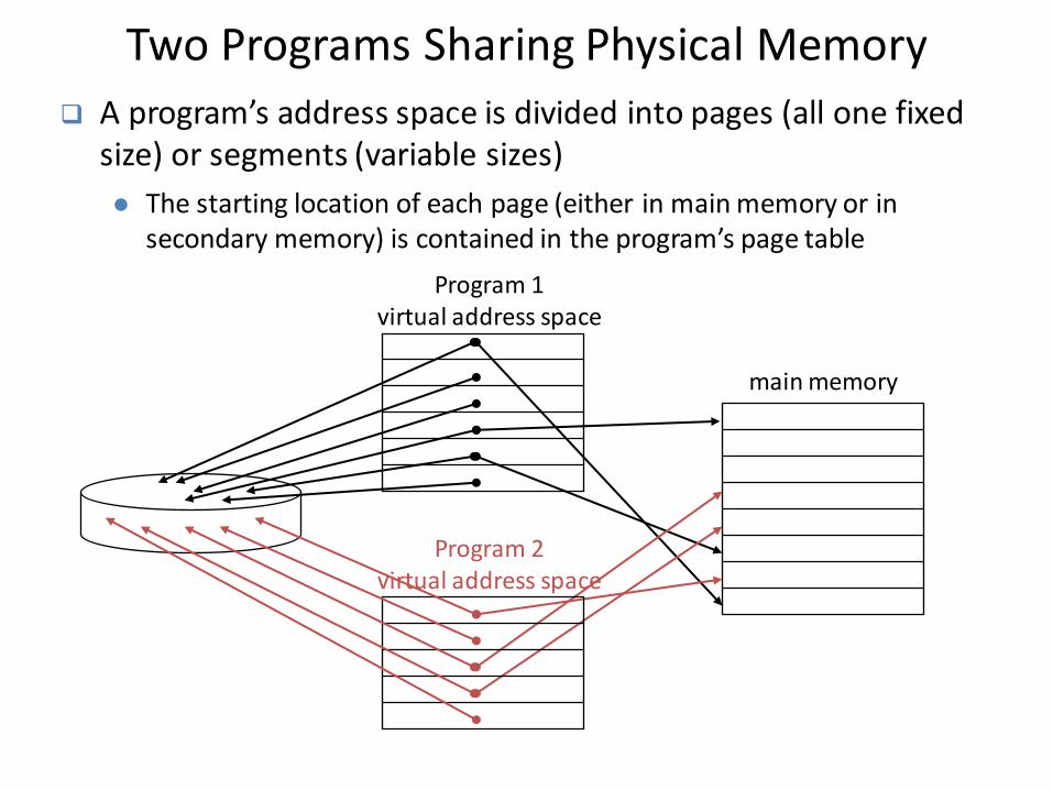
Two Programs Sharing Physical Memory
Program 1 virtual address space
main memory
A program’s address space is divided into pages (all one fixed size) or segments (variable sizes)
The starting location of each page (either in main memory or in secondary memory) is contained in the program’s page table
Program 2 virtual address space

Address Translation
Virtual Address (VA)
Page offset Virtual page number
31 30 . . . 12 11 . . . 0
Page offset Physical page number
Physical Address (PA) 29 . . . 12 11 0
Translation
• So each memory request first requires an address translation from the virtual space to the physical space – A virtual memory miss (i.e., when the page is not in
physical memory) is called a page fault
A virtual address is translated to a physical address by a combination of hardware and software

Address Translation Mechanisms
Physical page base addr
Main memory
Disk storage
Virtual page #
V 1 1 1 1 1 1 0 1 0 1 0
Page Table (in main memory)
Offset
Physical page #
Offset
Page
tab
le r
egis
ter

Virtual Addressing with a Cache • Thus it takes an extra memory access to translate a VA
to a PA
CPU Trans- lation
Cache Main
Memory
VA PA miss
hit data
This makes memory (cache) accesses very expensive (if every access was really two accesses)
The hardware fix is to use a Translation Lookaside Buffer (TLB) – a small cache that keeps track of recently used address mappings to avoid having to do a page table lookup

Making Address Translation Fast
Physical page base addr
Main memory
Disk storage
Virtual page #
V 1 1 1 1 1 1 0 1 0 1 0
1 1 1 0 1
Tag Physical page
base addr V
TLB
Page Table (in physical memory)
Page
tab
le r
egis
ter

Translation Lookaside Buffers (TLBs) • Just like any other cache, the TLB can be organized as
fully associative, set associative, or direct mapped
V Virtual Page # Physical Page # Dirty Ref Access
TLB access time is typically smaller than cache access time (because TLBs are much smaller than caches)
TLBs are typically not more than 512 entries even on high end machines

A TLB in the Memory Hierarchy
• A TLB miss – is it a page fault or merely a TLB miss? – If the page is loaded into main memory, then the TLB miss can be
handled (in hardware or software) by loading the translation information from the page table into the TLB
• Takes 10’s of cycles to find and load the translation info into the TLB
– If the page is not in main memory, then it’s a true page fault • Takes 1,000,000’s of cycles to service a page fault
• TLB misses are much more frequent than true page faults
CPU TLB
Lookup Cache
Main Memory
VA PA miss
hit
data
Trans- lation
hit
miss
¾ t ¼ t

TLB Event Combinations TLB Page
Table
Cache Possible? Under what circumstances?
Hit Hit Hit
Hit Hit Miss
Miss Hit Hit
Miss Hit Miss
Miss Miss Miss
Hit Miss Miss/
Hit
Miss Miss Hit
Yes – what we want!
Yes – although the page table is not checked if the TLB hits
Yes – TLB miss, PA in page table
Yes – TLB miss, PA in page table, but data not in cache
Yes – page fault
Impossible – TLB translation not possible if page is not present in memory
Impossible – data not allowed in cache if page is not in memory

Handling a TLB Miss • Consider a TLB miss for a page that is present in memory
(i.e., the Valid bit in the page table is set) – A TLB miss (or a page fault exception) must be asserted by the
end of the same clock cycle that the memory access occurs so that the next clock cycle will begin exception processing
Register CP0 Reg # Description
EPC 14 Where to restart after exception
Cause 13 Cause of exception
BadVAddr 8 Address that caused exception
Index 0 Location in TLB to be read/written
Random 1 Pseudorandom location in TLB
EntryLo 2 Physical page address and flags
EntryHi 10 Virtual page address
Context 4 Page table address & page number

A MIPS Software TLB Miss Handler • When a TLB miss occurs, the hardware saves the address
that caused the miss in BadVAddr and transfers control to 8000 0000hex, the location of the TLB miss handler
TLBmiss:
mfc0 $k1, Context #copy addr of PTE into $k1
lw $k1, 0($k1) #put PTE into $k1
mtc0 $k1, EntryLo #put PTE into EntryLo
tlbwr #put EntryLo into TLB
# at Random
eret #return from exception
tlbwr copies from EntryLo into the TLB entry selected by the control register Random
A TLB miss takes about a dozen clock cycles to handle

Some Virtual Memory Design Parameters
Paged VM TLBs
Total size 16,000 to
250,000 words
16 to 512
entries
Total size (KB) 250,000 to
1,000,000,000
0.25 to 16
Block size (B) 4000 to 64,000 4 to 8
Hit time 0.5 to 1
clock cycle
Miss penalty (clocks) 10,000,000 to
100,000,000
10 to 100
Miss rates 0.00001% to
0.0001%
0.01% to
1%

Two Machines’ TLB Parameters Intel Nehalem AMD Barcelona
Address sizes 48 bits (vir); 44 bits (phy) 48 bits (vir); 48 bits (phy)
Page size 4KB 4KB
TLB organization L1 TLB for instructions
and L1 TLB for data per
core; both are 4-way set
assoc.; LRU
L1 ITLB has 128 entries,
L2 DTLB has 64 entries
L2 TLB (unified) is 4-way
set assoc.; LRU
L2 TLB has 512 entries
TLB misses handled in
hardware
L1 TLB for instructions and
L1 TLB for data per core;
both are fully assoc.; LRU
L1 ITLB and DTLB each
have 48 entries
L2 TLB for instructions and
L2 TLB for data per core;
each are 4-way set assoc.; round robin LRU
Both L2 TLBs have 512
entries
TLB misses handled in
hardware

Why Not a Virtually Addressed Cache? • A virtually addressed cache would only require address
translation on cache misses
data
CPU Trans- lation
Cache
Main Memory
VA
hit
PA
but
Two programs which are sharing data will have two different virtual addresses for the same physical address – aliasing – so have two copies of the shared data in the cache and two entries in the TBL which would lead to coherence issues
- Must update all cache entries with the same physical address or the memory becomes inconsistent

Reducing Translation Time • Can overlap the cache access with the TLB access
– Works when the high order bits of the VA are used to access the TLB while the low order bits are used as index into cache
Tag Data
=
Tag Data
=
Cache Hit Desired word
VA Tag PA Tag
TLB Hit
2-way Associative Cache
Index
PA Tag
Block offset
Page offset Virtual page #

The Hardware/Software Boundary • What parts of the virtual to physical address
translation is done by or assisted by the hardware? – Translation Lookaside Buffer (TLB) that caches the recent
translations • TLB access time is part of the cache hit time • May allot an extra stage in the pipeline for TLB access
– Page table storage, fault detection and updating • Page faults result in interrupts (precise) that are then handled by
the OS
• Hardware must support (i.e., update appropriately) Dirty and Reference bits (e.g., ~LRU) in the Page Tables
– Disk placement • Bootstrap (e.g., out of disk sector 0) so the system can service a
limited number of page faults before the OS is even loaded

Cache Summary

4 Questions for the Memory Hierarchy
• Q1: Where can a entry be placed in the upper level? (Entry placement)
• Q2: How is a entry found if it is in the upper level? (Entry identification)
• Q3: Which entry should be replaced on a miss? (Entry replacement)
• Q4: What happens on a write? (Write strategy)

Q1&Q2: Where can a entry be placed/found?
# of sets Entries per set
Direct mapped # of entries 1
Set associative (# of entries)/ associativity Associativity (typically
2 to 16)
Fully associative 1 # of entries
Location method # of comparisons
Direct mapped Index 1
Set associative Index the set; compare
set’s tags
Degree of
associativity
Fully associative Compare all entries’ tags
Separate lookup (page)
table
# of entries
0

Q3: Which entry should be replaced on a miss?
• Easy for direct mapped – only one choice
• Set associative or fully associative – Random
– LRU (Least Recently Used)
• For a 2-way set associative, random replacement has a miss rate about 1.1 times higher than LRU
• LRU is too costly to implement for high levels of associativity (> 4-way) since tracking the usage information is costly

Q4: What happens on a write? • Write-through – The information is written to the entry in
the current memory level and to the entry in the next level of the memory hierarchy – Always combined with a write buffer so write waits to next level
memory can be eliminated (as long as the write buffer doesn’t fill)
• Write-back – The information is written only to the entry in the current memory level. The modified entry is written to next level of memory only when it is replaced. – Need a dirty bit to keep track of whether the entry is clean or
dirty – Virtual memory systems always use write-back of dirty pages to
disk
• Pros and cons of each? – Write-through: read misses don’t result in writes (so are simpler
and cheaper), easier to implement
– Write-back: writes run at the speed of the cache; repeated writes require only one write to lower level

Summary • The Principle of Locality:
– Program likely to access a relatively small portion of the address space at any instant of time. • Temporal Locality: Locality in Time
• Spatial Locality: Locality in Space
• Caches, TLBs, Virtual Memory all understood by examining how they deal with the four questions 1. Where can entry be placed?
2. How is entry found?
3. What entry is replaced on miss?
4. How are writes handled?
• Page tables map virtual address to physical address – TLBs are important for fast translation
Memory and Storage Implementations

SRAM / DRAM / Flash / RRAM / HDD Content Addressable SRAM cell

SRAM / DRAM / Flash / RRAM/ HDD

DRAM capacity growth

SRAM / DRAM / Flash / RRAM / HDD

• Purpose
– Long term, nonvolatile storage
– Lowest level in the memory hierarchy
• slow, large, inexpensive
• General structure
– A rotating platter coated with a magnetic surface
– A moveable read/write head to access the information on the disk
• Typical numbers
– 1 to 4 platters (each with 2 recordable surfaces) per disk of 1” to 3.5” in diameter
– Rotational speeds of 5,400 to 15,000 RPM
– 10,000 to 50,000 tracks per surface
• cylinder - all the tracks under the head at a given point on all surfaces
– 100 to 500 sectors per track
• the smallest unit that can be read/written (typically 512B)
Track
Sector
SRAM / DRAM / Flash / RRAM / HDD

Magnetic Disk Characteristic • Disk read/write components
1. Seek time: position the head over the proper track (3 to 13 ms avg) • due to locality of disk references
the actual average seek time may be only 25% to 33% of the advertised number
2. Rotational latency: wait for the desired sector to rotate under the head (½ of 1/RPM converted to ms) • 0.5/5400RPM = 5.6ms to 0.5/15000RPM = 2.0ms
3. Transfer time: transfer a block of bits (one or more sectors) under the head to the disk controller’s cache (70 to 125 MB/s are typical disk transfer rates in 2008) • the disk controller’s “cache” takes advantage of spatial locality in
disk accesses – cache transfer rates are much faster (e.g., 375 MB/s)
4. Controller time: the overhead the disk controller imposes in performing a disk I/O access (typically < .2 ms)
Sector
Track
Cylinder
Head Platter
Controller +
Cache

Acknowledgments
Some of the slides contain material developed and copyrighted by M.J. Irwin (Penn state) and instructor material for the textbook