meet automotive esd and seed requirements with zynq ... · esd protection of the zynq ultrascale+...
TRANSCRIPT

WP500 (v1.0) February 13, 2018 www.xilinx.com 1
© Copyright 2018 Xilinx, Inc. Xilinx, the Xilinx logo, Artix, ISE, Kintex, Spartan, Virtex, Vivado, Zynq, and other designated brands included herein are trademarks of Xilinx in the United States and other countries. All other trademarks are the property of their respective owners.
For designs that require safety and long-term reliability, Zynq UltraScale+ MPSoCs offer flexibility and design solutionsthat are perfect for leading-edge technologies, and meetautomotive ESD and SEED requirements.
White Paper: Zynq UltraScale+ MPSoCs
WP500 (v1.0) February 13, 2018
Meet Automotive ESD and SEED Requirements with Zynq UltraScale+ MPSoCs
By: James Karp, Michael J. Hart, Wai Kooi Wong, Krimo Semmoud, and Desmond Yeo
ABSTRACTThe automotive industry has established rigorously stringent requirements for:
• High reliability• Hostile environments• Low return rates• Long lifespan
Protection against Electrostatic Discharge (ESD) events is a key design parameter enabling this.Electronic equipment ESD safety is guaranteed with two levels of ESD protection: On-chip component level and system level. The latter is implemented with dedicated components mounted on a PCB.This white paper describes ESD protection of the 16nm Zynq® UltraScale+™ MPSoC and highlights its advantages for integration into highly demanding automotive System Efficient ESD Design (SEED).

WP500 (v1.0) February 13, 2018 www.xilinx.com 2
Meet Automotive ESD and SEED Requirements with Zynq UltraScale+ MPSoCs
IntroductionXilinx® ESD white paper WP433 [Ref 1] summarized how “Moore's Law,” the scaling trend of the semiconductor industry, leads to a reduction in component-level ESD immunity. Starting with 28nm 7 series devices, ESD immunity of Xilinx FPGAs was scaled down by about 50% as compared to the previous generations. To compensate for and mitigate against this ESD scaling, customers introduced stricter ESD-controlled environments at their manufacturing sites. Nevertheless, application ESD environments remained unchanged.
The increasing gap between component and system ESD requirements became an ongoing concern, especially for automotive applications. The latter presents the most hostile user ESD environment, and therefore in need of the most stringent system-level ESD specification. Consequently, the automotive industry is reluctant to accept scaling of component ESD immunity and continues to adhere to legacy ESD component targets [Ref 2]. To address the widening gap between component and system ESD specifications, the industry came up with the new System Efficient ESD Design (SEED) methodology that calls for co-design of onboard and on-chip ESD protections to achieve the goals of system-level ESD robustness [Ref 3][Ref 4]. The Zynq UltraScale+ MPSoC is the Xilinx All Programmable device with ESD protection designed to readily enable SEED and thus achieve system-level ESD goals.
This white paper describes ten ESD protection features in the Zynq UltraScale+ MPSoC that significantly facilitate SEED. It demonstrates the sufficiency of two ESD parameters, 150V charge device model (CDM) and 1500V human body model (HBM), to satisfy both automotive component level ESD and SEED. This white paper evaluates automotive applications relevant to SEED and highlights a loophole in the existing system-level ESD qualification that can result in undetected leakage-related ESD damage. The enhanced system-level ESD qualification methodology proposes that component and system ESD rejection criteria match. This approach greatly raises the barrier against ESD damage slipping into the system during PCB manufacturing or originating during the Zynq UltraScale+ MPSoC’s use.
Component-Level and System-Level ESDComponent- and system-level ESD protection is the primary goal of ESD-safe electronics. During manufacturing, handling, and testing of Zynq UltraScale+ MPSoCs, the HBM and the CDM are sufficient test methods to ensure yield and reliability [Ref 1]. However, these requirements are no longer applied after the device is assembled into a system—e.g., Automotive Driver Assistance Systems (ADAS). System-level ESD tests are defined by the International Electrotechnical Commission IEC 61000-4-2 ESD standard [Ref 5], or in automotive applications by the International Organization for Standardization ISO 10605 standard [Ref 6]. In addition, automotive manufacturers often have their own internal ESD qualification standard—e.g., FMC1278 for Ford Motor Company [Ref 7].
Zynq UltraScale+ MPSoCs provide sufficient ESD protection for automotive and SEED applications. The following are component- and system-level ESD qualification tests that are used to qualify the Xilinx devices.

WP500 (v1.0) February 13, 2018 www.xilinx.com 3
Meet Automotive ESD and SEED Requirements with Zynq UltraScale+ MPSoCs
HBM TestHBM refers to a human charge that discharges through the skin to an unpowered IC. It is always between two or more pins. Zynq UltraScale+ MPSoC’s minimum passing HBM voltage = 1,500V for I/Os and meets the automotive target of 2,000V [Ref 8] for any supply pin.
HBM stress simulated/tested with the HBM tester. During HBM stress, the IC is never exposed to HBM voltage(1) because the resistivity of human skin converts 1,500V HBM potential into HBM current, as shown in Equation 1:
Equation 1
where Rskin is modeled as a 1,500Ω resistor. A 1,500V HBM pulse corresponds to a current amplitude of ≈1.0A, a rise time of ≈ 5–10ns, and a decay time of ≈ 150ns.
It is important to note that HBM is not a real ESD threat because, for all practical purposes, human contact with Zynq UltraScale+ MPSoCs is eliminated both at the supplier and customer manufacturing facilities. Instead, HBM does play a significant role in SEED.
CDM TestCDM is the only real-world ESD event, occurring when electrostatic charge builds up on an unpowered IC and is then discharged via a single IC pin to ground. CDM discharge is simulated/tested with the CDM tester, which generates CDM stress pulses. For Zynq UltraScale+ MPSoCs, the minimum passing CDM voltage = 150V and typically is more than doubled for supply pins. This is in compliance with the automotive C2 CDM component classification, ranging from 125V to <250V [Ref 9]. The amplitude of the CDM stress is a weak function of die/package size [Ref 10]. For Zynq UltraScale+ MPSoCs, a 150V CDM pulse corresponds to a current amplitude of ≈ 3.0A with a rise time of ≈ 200–300ps and a decay time of ≈ 1–2ns.
CDM stress in a real-world industrial context is typically caused by tribology charges accumulating on an IC during contact with the environment—e.g., an IC sliding along a feeding tube, or moved with a robotic arm through ionized air. These charges are discharged when the IC comes into contact with a grounded metal—e.g., an ATE socket.
Latch-Up and Over-Voltage TestsZynq UltraScale+ MPSoCs pass the latch-up ±100mA injection and 50% supply overvoltage specification and is in compliance with automotive specifications [Ref 11].
1. The so-called “no connection” pins—that is, floating package pins that are not connected to the die—see full HBM voltage.
IHBMVHBMRskin----------- 1500
1500---------- 1A= = =

WP500 (v1.0) February 13, 2018 www.xilinx.com 4
Meet Automotive ESD and SEED Requirements with Zynq UltraScale+ MPSoCs
System-Level Test The system-level test is both a power-on and a power-off PCB test that reflects a user-uncontrolled ESD environment. An “ESD gun” imitates ESD events in both contact- and air-discharge modes. The former simulates ESD stress directly accessing a system; the latter simulates discharge close to a system, aiming to evaluate protection against electromagnetic interference (EMI). A comprehensive review of system-level ESD standards and testing are included in the References section [Ref 3].
Figure 1 shows ESD stresses at the same scale to illustrate that there is more than an order of magnitude difference between component CDM, HBM, and system ESD. It also illustrates the SEED concept, where ESD discharge is shared between onboard transient voltage suppressors (TVS) and on-chip ESD protection [Ref 3].
CDM/HBM Design and Interaction with SEEDThe prime consideration of on-chip CDM design is to ensure low IR drop in any charge-escape path during CDM discharge. With 3A of CDM current, even 1Ω resistance in the CDM discharge path can result in 3V of stress across transistors. With Moore’s Law, smaller transistor dimensions result in lessened electrical strength (the key FinFET transistor breakdown parameters are in the range of just 2–3 volts). That is why the CDM roadmap is descending, setting a 125V CDM limit for both 20nm and 16nm technology nodes [Ref 1]. Xilinx UltraScale and UltraScale+ families are manufactured, respectively, with 20nm and 16nm technology, exceeding roadmap requirements and meeting 150V CDM. Because there is no change in CDM immunity when progressing from 20nm to 16nm technology, the ESD safety certification for both process nodes is the same, facilitating customer migration from UltraScale to UltraScale+ devices.
X-Ref Target - Figure 1
Figure 1: ESD Stresses on Component CDM, HBM, and System ESD WP500_01_012218
ExternalProtection on PCB
Isolation Impedance
PCB TrackBypass Capacitor
Common Mode FIlterChip Ferrite Bead
30A
InternalProtection on IC
15A
50ns
8000V IEC
100ns
1000V HBM250V CDM
Residual Pulse Current
ExternalClamp(TVS)
InternalClamp
(IC’s ESDprotection)
TVS
ICO
WP500 (v1.0) February 13, 2018 www.xilinx.com 5
Meet Automotive ESD and SEED Requirements with Zynq UltraScale+ MPSoCs
HBM on-chip design differs from CDM in that it has to provide for low current density ( j HBM ) in the HBM discharge path. This is to avoid melting of both metallization and ESD elements. To lower j HBM, the ESD design relies on a larger cross-section of metallization and on larger ESD elements. Opposite to CDM criteria, HBM design criteria is mainly decoupled from the electrical strength of the transistors. Thus, it could appear that HBM strength is independent from Moore’s Law. This is not true where the HBM design affects I/O performance. Larger HBM elements have larger capacitance; this slows I/O speed and reduces bandwidth. From a performance point of view, the size of I/O ESD elements must be minimized. In Xilinx devices, the challenge of performance-ESD co-design is resolved by the use of a T-coil cancellation technique [Ref 12]. This innovation allows the 1,000V HBM industry roadmap to be superseded, achieving 32Gb/s (GT) transceiver performance with 1,500V HBM.
System-Level ESD ProtectionCharge Device Model (CDM): After the IC is mounted on the PCB, the CDM threat ceases to exist, as it is defined at component level. Therefore, attributes of on-chip CDM protection are no longer in use and do not support SEED. This assertion is supported by failure analysis statistics of 934 PCB designs with 9.5 billion shipped ICs. The study demonstrated the failure rate does not depend on CDM robustness [Ref 13].
Human Body Model (HBM): Unlike CDM, HBM becomes the prime SEED co-design parameter. HBM is modeled with a 100pF capacitor charged to 1,500V and discharged through a 1,500Ω resistor. IEC ESD stress is modeled with a 150pF capacitor charged to 8,000V and discharged through a 330Ω resistor. This leads to approximately the same time domain characteristics for both discharges (see Figure 1). This time domain similarity is the foundation for SEED co-design, where about 95% of system ESD discharge is diverted to ground through onboard ESD protection. The remaining small portion is defined as “residual pulse” and is diverted to ground with on-chip HBM resources (see Figure 1). Prior to ESD scaling, this sharing was tuned to 2,000V HBM. With ESD scaling, onboard protection had to be re-tuned to 1,000V HBM. To ease this re-tuning, the HBM robustness of Zynq UltraScale+ MPSoCs was enhanced to meet 1,500V for any I/O, and 2,000V for any supply rail.
Ten ESD Protection Features that Facilitate SEEDESD protection of the Zynq UltraScale+ MPSoC was designed and implemented with ten enhanced features, aiming to meet both automotive and SEED requirements.
1. ESD protection does not utilize latch-up-based silicon-controlled rectifiers (SCRs) and snap-back devices(1).
Over-voltage robustness is the key to safe automotive electronics. ESD or EMI transients can propagate into the device and trigger SCRs and snap-back ESD protection devices into a low-impedance state, subsequently causing damage to such ESD elements. To facilitate SEED, Zynq UltraScale+ devices do not use SCR/snap-back ESD protection.
1. VBATT is the only pin protected with the ultra-low-leakage snap-back device. VBATT is the battery backup supply for the encryption memory key; typically, automotive customers do not use this feature.

WP500 (v1.0) February 13, 2018 www.xilinx.com 6
Meet Automotive ESD and SEED Requirements with Zynq UltraScale+ MPSoCs
2. ESD protection is designed only with forward-biased ESD diodes and RC clamps.
During ESD transients, RC clamps are enabled and ESD diodes are switched into forward-biased mode (see Figure 2). However, current through these devices is self-limited by their intrinsic impedance; they are instantly returned to the off state, reverse-biased after ESD or EMI transients are suppressed with SEED.
3. All ESD devices are taken “as is” from TSMC-qualified ESD standard libraries with SPICE support.
TSMC standard ESD libraries are supported with high-current HSPICE ESD models. These curves are available for customers with IBIS package (available from I/O Specialists). It allows for ready alignment and unification of SEED solutions across the similar ESD protections on other ICs on the same PCB.
4. Isolated ground domains are coupled via the package ground plane or back-to-back diodes.
SEED design strategy is based on diverting any ESD transients to a PCB ground plane and then out to ground, or in the case of automotive implementation, to the common chassis. Items 4, 5, and 6 implement similar strategies for Zynq UltraScale+ MPSoCs. This significantly facilitates SEED.
5. ESD charges on any domain are first directed to the low-impedance ground plane and then out.
6. No ESD elements are between different voltage supplies.
7. Package supply-to-ground capacitors (≈ 1μF) provide chip ESD bypass.
The package power-to-ground decoupling capacitor is a low-impedance shunt for any ESD event and is by far the best ESD protection element (see Figure 2).
8. The four package corner pins are always connected to the package ground plane.
The automotive component CDM specification for corner pins is 750V [Ref 9], whereas the Zynq UltraScale+ MPSoC’s CDM is limited by high-performance I/Os and thus is approximately five times lower. To close this gap, two Zynq UltraScale+ MPSoCs (XAZU2EG and XAZU3EG assembled in the SBVA484 package) have four corner pins are connected to the GND package plane, thus ensuring high ESD immunity.
9. All voltage supplies by far exceed maximum 2,000V HBM automotive specification.
Zynq UltraScale+ MPSoC’s ESD protection of power supplies are designed with TSMC power clamps qualified to withstand 2,000V HBM and 500V CDM. By design, this ensures passing automotive HBM levels.
10. All I/Os are HBM-enhanced above industry-acceptable 1,000V to meet 1,500V.
A residual pulse can penetrate the device at the I/O pins, as shown in Figure 1. SEED must reduce the residual peak current to be lower than the I/O pin failure current under component-level HBM conditions. The higher the component HBM passing voltage, the easier the SEED task.
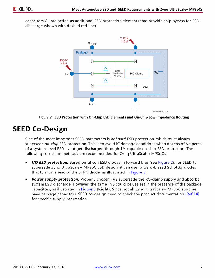
As illustrated in Figure 2, the Zynq UltraScale+ MPSoC’s ESD protection relies on both on-chip ESD elements (blue) and proprietary on-chip low-impedance ESD routing (green); package decoupling
WP500 (v1.0) February 13, 2018 www.xilinx.com 7
Meet Automotive ESD and SEED Requirements with Zynq UltraScale+ MPSoCs
capacitors CD are acting as additional ESD protection elements that provide chip bypass for ESD discharge (shown with dashed red line).
SEED Co-DesignOne of the most important SEED parameters is onboard ESD protection, which must always supersede on-chip ESD protection. This is to avoid IC damage conditions when dozens of Amperes of a system-level ESD event get discharged through 1A-capable on-chip ESD protection. The following co-design methods are recommended for Zynq UltraScale+MPSoCs:
• I/O ESD protection: Based on silicon ESD diodes in forward bias (see Figure 2), for SEED to supersede Zynq UltraScale+ MPSoC ESD design, it can use forward-biased Schottky diodes that turn on ahead of the Si PN diode, as illustrated in Figure 3.
• Power supply protection: Properly chosen TVS supersede the RC-clamp supply and absorbs system ESD discharge. However, the same TVS could be useless in the presence of the package capacitors, as illustrated in Figure 3 (Right). Since not all Zynq UltraScale+ MPSoC supplies have package capacitors, SEED co-design need to check the product documentation [Ref 14] for specific supply information.
X-Ref Target - Figure 2
Figure 2: ESD Protection with On-Chip ESD Elements and On-Chip Low Impedance Routing
WP500_02_012218
1500VHBM
2000V HBM
Supply
GND
I/O
Package
Zynq UltraScale+
MPSoCRC-Clamp
Chip
CD

WP500 (v1.0) February 13, 2018 www.xilinx.com 8
Meet Automotive ESD and SEED Requirements with Zynq UltraScale+ MPSoCs
SEED starts with the definition of external versus internal IC pins (see Figure 4). Transceiver and MIO pins on the device can be directly connected to the outside world. However, I/Os are typically buffered from direct external connections by other ICs on the board, e.g., memory, processor, camera, and powered by onboard precision voltage regulators. An example of such automotive application is shown in Figure 4.
Xilinx does receive RMAs, where internal pins have signature of Electrically Induced Physical Damage (EIPD), indicating that real world ESD and EMI events can couple to internal pins and cause EIPD. About 30% of customer returns have EIPD at the internal power supplies connected to precision voltage regulators, e.g., low-dropout (LDO). Usually this type of damage shows a distinct electrical over-stress (EOS) signature. To avoid supply damage, PCB designers must consider LDO with multiple protection features, including:
• Against all positive and negative pulses.
• Against reversed input polarity; in automotive, it means to survive improper jump starting.
• Input over-voltage shutdown. In automotive applications it is “load-dump protection” that happens, when the battery cable breaks loose and the alternator powers the vehicle.
• Output over-voltage shutdown. In case of poor or complete loss of the ground reference, the latter might force LDO operational amplifier to surge the output to a very high level.
X-Ref Target - Figure 3
Figure 3: Zynq UltraScale+ MPSoC On-Chip and Onboard Co-Design
X-Ref Target - Figure 4
Figure 4: Automotive Application Example
WP500_03_012318
V
Si (Schottky)GaAs (Schottky)Si PN
0.3 0.5 0.65 1.0
1.6
1.4
1.2
1
0.8
0.6
0.4
0.2
00 0.5 1 1.5
Vcc to GND withdecoupling capacitor
RC-clamp
TLP Voltage [V]
TLP
Cur
rent
[A]
2
WP500_04_012218
Micro-controller
12VCar Battery
GND: Negative battery terminalchassis not linked to the earth
Memory
FPGACameraMHi-Voltage
PowerManagement
IC
IC
ICIC
Circuit Board
External
bus
Con
nect
or
Internal

WP500 (v1.0) February 13, 2018 www.xilinx.com 9
Meet Automotive ESD and SEED Requirements with Zynq UltraScale+ MPSoCs
EMI is another major concern for SEED. Automotive EMI testing was conducted by sequentially increasing intensities of EM pulse [Ref 15]. Automobiles were in both “engine off” and “engine on” conditions. No EMI effects were observed in those automobiles that were “off” during EM pulse exposure. Malfunctions were observed only on running automobiles. Most of these running vehicles could not be immediately restarted. A battery had to be briefly disconnected for the vehicle to be restarted. Two key take-aways from these results: a) EMI cannot damage electronics in a powered-down mode, the latter being the condition for component-level ESD testing; b) EMI might trigger latch-up if the electronics are in a power-up mode. Latch-up current is between two terminals, supply and ground. “Fat” metallization is used to enable the 2,000V HBM of the Zynq UltraScale+ MPSoC supplies, which eases SEED against EMI.
“Walking Wounded”In reliability, the term “working wounded” refers to parts that have been damaged, yet not detected as failures, and are an ongoing concern [Ref 16]. What level of testing or screening is sufficient to show that there are no “walking wounded” devices? The Automotive Component Council Committee requires functional, parametric, or I-V verification “@ Room & Hot” for pre- and post-HBM, CDM, and latch-up qualification stress testing [Ref 2]. Zynq UltraScale+ MPSoC pass/fail criteria typically include leakage increase as compared with the fresh unit before the stress test. A much higher ESD stress is often needed to induce functional failure. The latter is often associated with EIPD. Thus, leakage increase, not EIPD or functional failure, sets the true limit for Zynq UltraScale+ MPSoCs’ ESD immunity.
Contrarily, the functionality of a board under test (BUT) is the pass/fail criteria for system-level ESD qualification [Ref 3]. This creates conditions where an incomplete SEED can be qualified. Systems with incomplete SEED can become “walking wounded” just as they can during system qualification. In the field, these undetected damages can evolve into functional damages and reported as RMAs. To close this loophole for the “walking wounded” during system-level ESD qualification, Xilinx proposes to match Zynq UltraScale+ MPSoC component and system-level pass/fail criteria [Ref 17] as follows:
1. Pre-ATE test: (1) All Zynq UltraScale+ devices to be on BUTs are ATE re-tested the same way as during component ESD qualification, with test results logged.
2. Post-ATE test: (1) After a system has been considered as “Pass ESD Qualification,” all Zynq UltraScale+ MPSoCs are demounted from BUTs, re-balled, and post-ATE tested.
3. Pre- and post-ATE results compared, with pass/fail criteria applied similar to ESD/Latch-up Zynq UltraScale+ MPSoC qualification.
1. Pre- and post-ATE test can be done at contractor test houses or, with proper arrangements, at Xilinx .

WP500 (v1.0) February 13, 2018 www.xilinx.com 10
Meet Automotive ESD and SEED Requirements with Zynq UltraScale+ MPSoCs
SummaryThe application of Moore’s Law scaling to component-level ESD immunity gave birth to system-efficient ESD design (SEED) methodology. SEED calls for the co-design of onboard and on-chip ESD protection to achieve the goals of system-level ESD robustness.
To meet these emerging requirements, the Zynq UltraScale+ MPSoC’s ESD protection was designed with ten SEED-friendly features. CDM immunity has no impact on system ESD design, where reduced 1,500V I/O HBM immunity versus a pre-scale 2,000V specification must be compensated for with SEED co-design. “Walking wounded” loopholes are known and identified in SEED qualification methodology; to close these loopholes, component and system-level pass/fail criteria must match.
Postscript:
Most American cars in the 1950s–1960s had sheet-metal thickness of around 0.05in. New cars use sheet metal of around 0.03in or thinner. However, human safety requirements for new cars is much higher than it used to be. These requirements have been met by implementation of seat belts, airbags, safety electronics, and many other technological innovations.
A similar trend has been observed in the ESD immunity of components, which has been scaling down in the manner of automotive sheet-metal thickness, and for the same reasons: cost and performance. Again, new solutions have been brought in—including SEED—to ensure safety of modern car electronics.
This white paper demonstrates Xilinx’s ongoing commitment to automotive safety and customer support in this important market space.

WP500 (v1.0) February 13, 2018 www.xilinx.com 11
Meet Automotive ESD and SEED Requirements with Zynq UltraScale+ MPSoCs
References1. J. Karp, M. J. Hart, and T. C. Chai, “Understanding and Mitigating System-Level ESD and EOS
Events in Xilinx 7 Series Devices”, Xilinx White Paper WP433 v1.0, June 24, 2013https://www.xilinx.com/support/documentation/white_papers/wp433-Mitigating-ESD-EOS.pdf
2. Failure Mechanism Based Stress Test Qualification For Integrated Circuits; AEC-Q100, Rev H, September 11, 2014http://www.aecouncil.com/Documents/AEC_Q100_Rev_H_Base_Document.pdf
3. “White Paper 3: System Level ESD, Part I: Common Misconceptions and Recommended Basic Approaches”, Rev 1.0, December 2010https://www.esda.org/about-esd/white-papers
4. C. Duvvury and H. Gossner, “System Level ESD Co-design”, IEEE Press, John Wiley & Son, West Sussex, UK, 2015
5. “Electromagnetic Compatibility (EMC), Part 4-2: Testing and Measurement Techniques— Electrostatic Discharge Immunity Test”, IEC 61000 4-2, 2008https://webstore.iec.ch/publication/4189
6. “Road vehicles—Test Methods for Electrical Disturbances from Electrostatic Discharge”, ISO Standard 10605, International Organization for Standardization, 2008https://www.iso.org/standard/41937.html
7. “Electromagnetic Compatibility (EMC) Requirements for Electrical/Electronic Components and Subsystems”, FMC1278, for Ford Motor Company (FMC)http://www.fordemc.com/docs/download/FMC1278.pdf
8. “Automotive Electronic Counsel HBM”, AEC-Q100-002 Rev-E, p. 5, August 20, 2013http://www.aecouncil.com/Documents/AEC_Q100-002E.pdf
9. “Automotive Electronic Counsel CDM”, AEC-Q100-011 Rev-C1, p. 12, March 12, 2013http://www.aecouncil.com/Documents/AEC_Q100-011C1.pdf
10. J. Karp, V. Kireev, D. Tsaggaris, and M. Fakhruddin, “Effect of Flip-Chip Package Parameters on CDM Discharge”, EOS/ESD Symposium, Tucson, AZ, 2008http://ieeexplore.ieee.org/document/4772108/
11. “Automotive Electronic Counsel Latch-Up”, AEC-Q100-004, p. 2, Rev-D, August 7, 2012http://www.aecouncil.com/Documents/AEC_Q100-004D.pdf
12. J. Karp, M. J. Hart, M. Fakhruddin, et al, “FinFET MPSoC 32Gb/s Transceivers: Custom ESD Protection and Verification”, 2016 IEEE 59th International Midwest Symposium on Circuits and Systems, October 2016http://ieeexplore.ieee.org/stamp/stamp.jsp?arnumber=7869952
13. “White Paper 2: A Case for Lowering Component Level CDM ESD Specifications and Requirements”, pp. 69–70, March 2009, Rev. 1.0.https://www.esda.org/about-esd/white-papers
14. Xilinx Zynq UltraScale+ MPSoC Packaging and Pinouts Product Specification, UG107515. J. Emanuelson, “EMP Effects on Vehicles”, Futurescience, LLC
http://www.futurescience.com/emp/vehicles.html16. J. E. Vinson et al, “ESD Design and Analysis Handbook”, p. 52, Kluwer Academic Publishers,
Norwell, MA, USA, 200317. J. Karp et al, “Automotive System Level ESD Qualification with Component Level Pass/Fail
Criteria”, to be published in proceedings of International ESD Workshop, Belgium, May, 2018

WP500 (v1.0) February 13, 2018 www.xilinx.com 12
Meet Automotive ESD and SEED Requirements with Zynq UltraScale+ MPSoCs
Additional ResourcesTo see a summary of the reliability test data and results for Xilinx devices, see UG116, Device Reliability Report. This report is updated two times per year.
Revision HistoryThe following table shows the revision history for this document:
DisclaimerThe information disclosed to you hereunder (the “Materials”) is provided solely for the selection and use of Xilinxproducts. To the maximum extent permitted by applicable law: (1) Materials are made available “AS IS” and with all faults,Xilinx hereby DISCLAIMS ALL WARRANTIES AND CONDITIONS, EXPRESS, IMPLIED, OR STATUTORY, INCLUDING BUT NOTLIMITED TO WARRANTIES OF MERCHANTABILITY, NON-INFRINGEMENT, OR FITNESS FOR ANY PARTICULAR PURPOSE;and (2) Xilinx shall not be liable (whether in contract or tort, including negligence, or under any other theory of liability)for any loss or damage of any kind or nature related to, arising under, or in connection with, the Materials (including youruse of the Materials), including for any direct, indirect, special, incidental, or consequential loss or damage (including lossof data, profits, goodwill, or any type of loss or damage suffered as a result of any action brought by a third party) evenif such damage or loss was reasonably foreseeable or Xilinx had been advised of the possibility of the same. Xilinxassumes no obligation to correct any errors contained in the Materials or to notify you of updates to the Materials or toproduct specifications. You may not reproduce, modify, distribute, or publicly display the Materials without prior writtenconsent. Certain products are subject to the terms and conditions of Xilinx’s limited warranty, please refer to Xilinx’sTerms of Sale which can be viewed at http://www.xilinx.com/legal.htm#tos; IP cores may be subject to warranty andsupport terms contained in a license issued to you by Xilinx. Xilinx products are not designed or intended to be fail-safeor for use in any application requiring fail-safe performance; you assume sole risk and liability for use of Xilinx productsin such critical applications, please refer to Xilinx’s Terms of Sale which can be viewed at http://www.xilinx.com/legal.htm#tos.
Automotive Applications DisclaimerAUTOMOTIVE PRODUCTS (IDENTIFIED AS “XA” IN THE PART NUMBER) ARE NOT WARRANTED FOR USE IN THEDEPLOYMENT OF AIRBAGS OR FOR USE IN APPLICATIONS THAT AFFECT CONTROL OF A VEHICLE (“SAFETYAPPLICATION”) UNLESS THERE IS A SAFETY CONCEPT OR REDUNDANCY FEATURE CONSISTENT WITH THE ISO 26262AUTOMOTIVE SAFETY STANDARD (“SAFETY DESIGN”). CUSTOMER SHALL, PRIOR TO USING OR DISTRIBUTING ANYSYSTEMS THAT INCORPORATE PRODUCTS, THOROUGHLY TEST SUCH SYSTEMS FOR SAFETY PURPOSES. USE OFPRODUCTS IN A SAFETY APPLICATION WITHOUT A SAFETY DESIGN IS FULLY AT THE RISK OF CUSTOMER, SUBJECT ONLYTO APPLICABLE LAWS AND REGULATIONS GOVERNING LIMITATIONS ON PRODUCT LIABILITY.
Date Version Description of Revisions02/13/2018 1.0 Initial Xilinx release.