mechanics-driven patterning of cvd graphene for roll-based...
TRANSCRIPT

This content has been downloaded from IOPscience. Please scroll down to see the full text.
Download details:
IP Address: 143.248.95.63
This content was downloaded on 20/02/2017 at 04:09
Please note that terms and conditions apply.
Mechanics-driven patterning of CVD graphene for roll-based manufacturing process
View the table of contents for this issue, or go to the journal homepage for more
2017 2D Mater. 4 024003
(http://iopscience.iop.org/2053-1583/4/2/024003)
Home Search Collections Journals About Contact us My IOPscience
You may also be interested in:
Damage mitigation in roll-to-roll transfer of CVD-graphene to flexible substrates
Bongkyun Jang, Chang-Hyun Kim, Seung Tae Choi et al.
Out-of-plane growth of CNTs on graphene for supercapacitor applications
Youn-Su Kim, Kitu Kumar, Frank T Fisher et al.
Transfer printing of graphene strip from the graphene grown on copper wires
Ching-Yuan Su, Dongliang Fu, Ang-Yu Lu et al.
Uniformity of large-area bilayer graphene grown by chemical vapor deposition
Yuewen Sheng, Youmin Rong, Zhengyu He et al.
Influence of the copper substrate roughness on the electrical quality of graphene
Gi Duk Kwon, Eric Moyen, Yeo Jin Lee et al.
Ultrasmooth metallic foils for growth of high quality graphene by chemical vapor deposition
Pavel Procházka, Jindich Mach, Dominik Bischoff et al.
Graphene decorated microelectrodes for simultaneous detection of ascorbic, dopamine, and folic
acids by means of chemical vapor deposition
N Namdar, M Hassanpour Amiri, F Dehghan Nayeri et al.
Engineering electrical properties of graphene: chemical approaches
Yong-Jin Kim, Yuna Kim, Konstantin Novoselov et al.
Synthesis, properties and applications of 3D carbon nanotube–graphene junctions
Chun-Yu Lin, Zhenghang Zhao, Jianbing Niu et al.

© 2017 IOP Publishing Ltd
Introduction
The outstanding electrical [1], optical [2], and mechanical properties of graphene make it a promising candidate for flexible [3] and transparent electrode applications [4]. Although there has been considerable effort to commercialize graphene as a transparent electrode [5], it is still less competitive compared to other, conventional transparent electrodes [6]. In order to allow for mass production of graphene, researchers have developed various cost-effective, scalable manufacturing processes to produce large-scale, high quality graphene films using chemical vapor deposition (CVD) growth, CVD-grown graphene films larger than 30 inches have been reported by Bae et al [5]. Moreover, the speed of synthesis has been significantly improved
using rapid heating methods such as a halogen heater [7] and the joule heating method [8]. The synthesized graphene can be transferred onto the desired substrate using a variety of methods such as the carrier film method [5, 9], bubble transfer method [10], or direct separation method from the copper foil [11, 12]. As evidenced by these developments, significant progress has been made toward large-scale synthesis and transfer of graphene, which could be integrated into a roll-to-roll manufacturing system for graphene electrodes. One of the most important challenges remaining for commercializing graphene electrodes is to develop a graphene patterning technique compatible with roll-to-roll manufacturing methods.
The conventional approach for patterning gra-phene is photolithography, which requires multiple
S-M Kim et al
024003
2D MATER.
© 2017 IOP Publishing Ltd
4
2D Mater.
2DM
2053-1583
10.1088/2053-1583/aa59af
2
1
8
2D Materials
IOP
8
February
2017
Mechanics-driven patterning of CVD graphene for roll-based manufacturing process
Sang-Min Kim1,4, Bongkyun Jang4, Kyungmin Jo2, Donghyuk Kim3,4, Jihye Lee4, Kyung-Shik Kim4, Seung-Mo Lee4, Hak-Joo Lee4, Seung Min Han1,5 and Jae-Hyun Kim4,5
1 Graduate School of Energy Environment Water and Sustainability, Korea Advanced Institute of Science & Technology (KAIST), Daejeon 34141, Korea
2 Center for Inorganic Analysis, Division of Metrology for Quality of Life, Korea Research Institute of Standards and Science (KRISS), Daejeon 34113, Korea
3 Department of Materials Science and Engineering, Korea Advanced Institute of Science & Technology (KAIST), Daejeon 34141, Korea4 Nano-Convergence Mechanical System Research Division, Korea Institute of Machinery & Materials (KIMM), Daejeon 34103, Korea5 Author to whom any correspondence should be addressed.
E-mail: [email protected] (J-H Kim) and [email protected] (S M Han)
Keywords: grapheme, roll-to-roll, patterning, supercapacitor
Supplementary material for this article is available online
AbstractGraphene is considered as a promising material for flexible and transparent electrodes due to its outstanding electrical, optical, and mechanical properties. Efforts to mass-produce graphene electrodes led to the development of roll-to-roll chemical vapor deposition (CVD) graphene growth and transfer, and the only remaining obstacle to the mass-production of CVD graphene electrodes is a cost-effective patterning technique that is compatible with the roll-to-roll manufacturing. Herein, we propose a mechanics-driven technique for patterning graphene synthesized on copper foil (commonly used in roll-to-roll manufacturing). The copper foil is exposed to high temperature for a prolonged period during the CVD growth of graphene, and thus can result in recrystallization and grain growth of the copper foil and thereby reducing to the yield strength. This softening behavior of the copper was carefully controlled to allow simple stamp patterning of the graphene. The strength of the underlying substrate was controlled for the accuracy of the residual patterns. The proposed stamp patterning technique is mask-less and photoresist-free, and can be performed at room temperature without high-energy sources such as lasers or plasma. To demonstrate the capability of this process to produce a continuous electrode, a transparent in-plane supercapacitor was fabricated using the proposed patterning technique.
PAPER2017
RECEIVED 3 September 2016
REVISED
5 December 2016
ACCEPTED FOR PUBLICATION
16 January 2017
PUBLISHED 8 February 2017
doi:10.1088/2053-1583/aa59af2D Mater. 4 (2017) 024003

2
S-M Kim et al
steps that include photoresist (PR) coating, UV expo-sure, PR developing, graphene etching, and PR removal [13]. Because these multiple steps deteriorate the cost-effectiveness of roll-to-roll manufacturing, alternative methods such as laser-assisted transfer printing [14], micro molding method using polydimethylsiloxane (PDMS) stamps [15–17], and the photo-roll lithogra-phy method [18] have been suggested to improve the simplicity and productivity of the patterning process. However, these conventional methods suffer from the need for expensive laser irradiation, low durability of the PDMS stamps, and multiple expensive steps of UV exposure and PR processing, respectively. Therefore, a cost-effective patterning technology remains as the only obstacle limiting the roll-to-roll manufacturing of graphene electrode films [19].
In this study, we present a novel roll-based pattern-ing technology for producing CVD graphene that does not rely on a high-energy source, or UV exposure and PR process. This technology was realized by making use of the softening behavior of Cu foil (the catalyst sub-strate for graphene growth), then using highly durable Ni stamps to pattern the graphene at room temperature. This roll-based patterning process is suitable for scaling up the patterning area and achieving high productivity in roll-to-roll manufacturing of CVD graphene, but has difficulty in accurate alignment compared to conven-tional optical mask aligners for semiconductor process. Considering this alignment issue, the main applications for the proposed method could be for bottom elec-trodes of flexible and transparent electronic devices, and some electrical or electrochemical elements like supercapacitors.
Results
Microstructural change of Cu foils during synthesis of grapheneThermal CVD is a well-known process in which Cu foil is exposed to H2 and carbon-gas precursor (such as C2H4 or CH4) compounds at high temperature that decompose on the surface of the Cu to feed the graphene growth [20–22]. During CVD graphene growth, the high temperature annealing process plays an essential role in the Cu grain growth. As-received Cu foils exhibit small grain sizes (confirmed by EBSD analysis). Small grain size then results in strengthening, according to the Hall–Petch relation, where the yield strength of Cu is expected to increase with reduction of
grain size ( /σ d~ 1YS ) [23]. As the Cu foil is subjected to heat treatment, the yield strength of the Cu foil can decrease as grain growth occurs. This phenomenon was used as means to control the strength of the underlying foil for more precise graphene patterning [24, 25].
Cu foil samples were annealed in Ar gas (300 sccm) at different temperatures of 200, 400, 600, 800 and 1000 °C for 1 h in a tube furnace CVD chamber of 4 inch diameter under 640 mTorr. The tube furnace CVD chamber was also utilized for graphene growth. With
respect to the melting point of Cu (1083 °C), these temper atures correspond to 18%, 37%, 55%, 74% and 92%, of the melting temperature. Mechanical charac-terization was conducted using nano-indentation (MTS Nanoindenter XP) and and using tensile testing (Uni-versal Testing Machine RB 302 ML). Nano-indentations were conducted up to a load of 500 mN in continuous stiffness mode, with a Berkovich tip. Tensile tests were conducted using a dog bone specimen of the standard ASTM geometry. Scanning electron microscopy with electron-backscatter diffraction (SEM-EBSD) was used to characterize changes in the Cu microstructure as a function of the annealing temper ature.
The nano-indentation test results in figure 1(a) showed that the hardness (as analyzed by the Oliver and Pharr method) of the as-received Cu was 2 GPa while that of the Cu annealed at 1000 °C was 0.75 GPa and the hardness of Ni stamp was 4.8 GPa. Even when annealed at 200 °C, the hardness of the Cu foil dramatically decreased (by ~50%). EBSD analysis showed increase of grain size with increase of the annealing temperature. Drastic differences in grain size occurred, from several micrometers (average diameter: 5.9 ± 0.8 µm) to over tens of micrometers (average diameter: 75 ± 16 µm) in as-received and 1000 °C annealed Cu foil respectively. It is noteworthy that as-received Cu foils have micro-crystalline structures which result in high hardness. Similarly, the tensile test results in figure 1(b) showed dramatic decrease in yield strength with increase in the annealing temperature. The yield strength (5% offset strength) of the as-received Cu foils was 380 MPa, while that of the Cu foils annealed at 1000 °C was 21 MPa. For precise patterning of the Cu foils via mechanical imprinting, it is beneficial to have a substrate with lower strength so that the stamp pattern transfers clearly onto the substrate, as shown in figure 1(c). Therefore, we take advantage of the softening mechanism of Cu induced by high-temperature annealing during CVD graphene synthesis and develop a simple and efficient roll-based method for graphene patterning. We utilized a roll-to-plate transfer machine to demonstrate the proposed patterning method, and it is straightforward to replace the roll-to-plate machine with a roll-to-roll machine.
Mechanics-driven patterning of CVD graphene under room temperature
Based on the softening mechanism of Cu that occurs during high-temperature growth of graphene, the graphene was patterned by imprinting a patterned Ni stamp on Cu foils coated with CVD graphene. Ni was selected as the stamp material because it has higher hardness than Cu and is easy to handle. A Ni stamp with strip patterns of 30 µm pitch, 5 µm linewidth, and 10 µm height was prepared by electroplating a 2 mm thick Ni film on a pre-patterned silicon wafer and then the electrodeposited Ni film is separated from the wafer. The roller stamp was prepared by attaching a 2 cm × 2 cm patterned Ni stamp to a roller. The
2D Mater. 4 (2017) 024003

3
S-M Kim et al
roll-to-plate transfer machine has a roller with a width of 150 mm and a diameter of 170 mm. A proportional-integral-derivative (PID) feedback module coupled with two load-cells and two z-axis actuators controls the stamping load via the roller stamp. The stamping load has a significant impact on the pattern fidelity, and the pattern uniformity is affected by the uniformity in the load distribution in the directions of rolling and the roll axis. In order to ensure the contact between the stamp and the Cu foil, the automated roller stamp was slowly moved along the z-axis until the stamping load reached 10 N. After ensuring the contact, the roller stamp was moved further until the prescribed stamping load was achieved, then rolling of the stamp started and proceeded at 60 mm min−1 during the patterning step. The schematic for patterning the graphene is shown in figure 2(a). First, Cu foils were annealed at high temperature (1000 °C) for CVD growth of graphene using the conditions reported in [26]. Second, Cu foil coated with CVD graphene was placed under a Ni stamp and was applied with a pre-scribed load. The
achievable minimum pattern could be dependent on substrate thickness, surface roughness, stamp geometry, and stamping process. The thickness of Cu can affect the incompressible deformation of Cu during the stamping process. When the thickness is much larger than the pattern height, the required patterning load is nearly independent of the thickness. On the other hand, when the thickness is comparable to the pattern height, the required patterning load is largely affected by the thickness. The roughness has more profound effect on the patterning process. When the roughness is larger than the pattern height or spacing, it is difficult to obtain uniform patterns over a wide area. Third, a carrier film was attached to the patterned CVD graphene and the Cu foil was removed by etching in ammonium persulfate (APS) solution [27]. Graphene on the impressed region in the Cu foil by the Ni stamp was unable to make contact with the carrier film, and was washed away during the Cu foil etching process. Finally, the remaining graphene pattern on the carrier film was transferred to the target substrate. Raman
Figure 1. Softening mechanics of Cu foil by heat treatments: (a) the hardness and EBSD data of Cu foils after annealing under given temperatures for 1 h in a furnace. (b) Tensile test results of as-received and annealed Cu foils. (c) The influence of annealing temperature (annealing time for 1 h) on the hardness. Photograph of as-received and annealed Cu foil roll-pressed with a coin stamp.
2D Mater. 4 (2017) 024003

4
S-M Kim et al
spectroscopy confirmed that the patterning process did not degrade the quality of the graphene, as shown in figure S1 (stacks.iop.org/TDM/4/024003/mmedia). It is important to note that a softer Cu foil requires lower imprinting pressure. Therefore, the resolution and process conditions of imprinting are greatly affected by the mechanical properties of the annealed Cu foil, where softer Cu with small hardness results in larger impression in the ‘stamped’ section (under same applied load to the Ni stamp) and thus allow for the carrier film to be in contact with only the ‘non-pressed’ portion for cleaner transfer of the patterned graphene film. The effect of different strength of Cu foil will be quantitatively examined by finite element analysis in the following section.
The fabricated graphene patterns were analyzed using atomic force microscopy (AFM). The dimen-sions of the patterns on the Ni stamp, and on the Cu foil coated by graphene, are shown in figures 2(b) and (c). Three types of Cu foils with different annealing temper-atures were compared under the identical imprinting load of 80 N (figure 2(d)). We tested the stamping loads of 0, 20, 40, 60, and 80 N, respectively (figure S2) to make patterns on the graphene grown Cu foils. With the stamping loads less than 80 N, the pattern transfer became incomplete because of the surface roughness and the grain boundaries of the Cu foils, which prevent conformal contact between the stamp and the Cu foils. For this specific type of pattern, it is required to have a stamping load over the 80 N for uniform patterns. The height of the imprinted pattern increased with increase
of the annealing temperature while the pitch of the pat-tern remained unchanged. Owing to the ultra-low yield strength of the annealed Cu foil at 1000 °C, the pattern fidelity between the Ni stamp and the Cu foil was very high. Pattern formation based on the proposed technol-ogy can be scaled down to sub-micron scale or scaled up to micron scale. Creating a microscale radio frequency identification (RFID) antenna with a line width of 5 µm, and nanoscale donut patterns with a line width of 200 nm was successfully demonstrated (figure S3). However, these methods promote the graphene appli-cation needed to integrating into a roll-to-roll system overcome alignment limitation for electronic devices such as thin film transistor (TFT) devices structure. To extend this method for the graphene based application need further studies to improve alignment issues in high precision patterning.
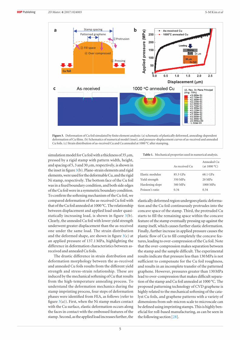
Finite element analysis of the mechanics-driven patterning process
Finite element analysis (FEA) was carried out using ABAQUS/Explicit to understand the softening mechanism behind the pattern formation. Figure 3(a) shows a schematic of the plastic deformation that occurs on the Cu foil during the patterning process. The material properties used in the FEA were derived from tensile testing shown in figure 1 and are listed in table 1. The yield strength of the Cu foil was taken to be equivalent to the experimentally determined values that are dependent on the annealing temperatures. A
Figure 2. Mechanics-driven patterning of CVD graphene: (a) schematic of graphene patterning process based on softening mechanics of Cu foils. The optical microscope image represents a patterned graphene (Gr)-coated Cu foil piece with Ni stamp. The AFM image of (b) a Ni Stamp, (c) patterned graphene on Cu, and (d) cross-sectional profile for as-received Cu, and annealed Cu at 200 and 1000 °C.
2D Mater. 4 (2017) 024003
5
S-M Kim et al
simulation model for Cu foil with a thickness of 35 µm, pressed by a rigid stamp with pattern width, height, and spacing of 5, 3 and 30 µm, respectively, is shown in the inset in figure 3(b). Plane-strain elements and rigid elements, were used for the deformable Cu, and the rigid Ni stamp, respectively. The bottom face of the Cu foil was in a fixed boundary condition, and both side edges of the Cu foil were in a symmetric boundary condition. To confirm the softening mechanism of the Cu foil, we compared deformation of the as-received Cu foil with that of the Cu foil annealed at 1000 °C. The relationship between displacement and applied load under quasi-statically increasing load, is shown in figure 3(b). Clearly, the annealed Cu foil with lower yield strength underwent greater displacement than the as-received one under the same load. The strain distribution and the deformed shape, are shown in figure 3(c) at an applied pressure of 137.1 MPa, highlighting the difference in deformation characteristics between as-received and annealed Cu foils.
The drastic difference in strain distribution and deformation morphology between the as-received and annealed Cu foils results from the different yield strength and stress-strain relationship. These are induced by the mechanical softening of Cu that results from the high-temperature annealing process. To understand the deformation mechanics during the stamp imprinting process, four steps of deformation phases were identified from FEA, as follows (refer to figure 3(a)). First, when the Ni stamp makes contact with the Cu surface, elastic deformation occurs along the faces in contact with the embossed features of the stamp. Second, as the applied load increases further, the
elastically deformed region undergoes plastic deforma-tion and the Cu foil continuously protrudes into the concave space of the stamp. Third, the protruded Cu starts to fill the remaining space within the concave feature of the stamp eventually pressing up against the stamp itself, which causes further elastic deformation. Finally, further increase in applied pressure causes the plastic flow of Cu to fill completely the concave fea-tures, leading to over-compression of the Cu foil. Note that the over-compression makes separation between the stamp and the sample difficult. The experimental results indicate that pressure less than 130 MPa is not sufficient to compensate for the Cu foil roughness, and results in an incomplete transfer of the patterned graphene. However, pressures greater than 130 MPa lead to over-compression that makes difficult separa-tion of the stamp and Cu foil annealed at 1000 °C. The proposed patterning technology of CVD graphene is highly related to the mechanical softening of the cata-lyst Cu foils, and graphene patterns with a variety of dimensions from sub-micron scale to microscale can be defined using imprinting stamps. This is highly ben-eficial for roll-based manufacturing, as can be seen in the following section [28].
Figure 3. Deformation of Cu foil simulated by finite element analysis: (a) schematic of plastically deformed, annealing-dependent deformation of Cu films. (b) Schematics of numerical model (inset), and pressure-displacement curves of as-received and annealed Cu foils. (c) Strain distribution of as-received Cu and Cu annealed at 1000 °C after stamping.
Table 1. Mechanical properties used in numerical analysis.
As received Cu
Annealed Cu
(at 1000 °C)
Elastic modulus 85.3 GPa 68.1 GPa
Yield strength 350 MPa 20 MPa
Hardening slope 500 MPa 1000 MPa
Poisson’s ratio 0.34 0.34
2D Mater. 4 (2017) 024003
6
S-M Kim et al
Fabrication of an in-plane supercapacitor and its electrochemical performance
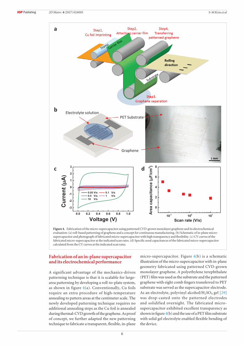
A significant advantage of the mechanics-driven patterning technique is that it is scalable for large-area patterning by developing a roll-to-plate system, as shown in figure 4(a). Conventionally, Cu foils require an extra procedure of high-temperature annealing to pattern areas at the centimeter scale. The newly developed patterning technique requires no additional annealing steps as the Cu foil is annealed during thermal-CVD growth of the graphene. As proof of concept, we further adapted the new patterning technique to fabricate a transparent, flexible, in-plane
micro-supercapacitor. Figure 4(b) is a schematic illustration of the micro-supercapacitor with in-plane geometry fabricated using patterned CVD-grown monolayer graphene. A polyethylene terephthalate (PET) film was used as the substrate and the patterned graphene with eight comb fingers transferred to PET substrate was served as the supercapacitor electrode. As an electrolyte, polyvinyl alcohol/H2SO4 gel [29] was drop-casted onto the patterned electrodes and solidified overnight. The fabricated micro-supercapacitor exhibited excellent transparency as shown in figure 4(b) and the use of a PET film substrate with solid gel electrolyte enabled flexible bending of the device.
Figure 4. Fabrication of the micro-supercapacitor using patterned CVD-grown monolayer graphene and its electrochemical evaluation: (a) roll-based patterning of graphene and a concept for continuous manufacturing. (b) Schematic of in-plane micro-supercapacitor and photograph of fabricated micro-supercapacitor with high transparency and flexibility. (c) CV curves of the fabricated micro-supercapacitor at the indicated scan rates. (d) Specific areal capacitances of the fabricated micro-supercapacitor calculated from the CV curves at the indicated scan rates.
2D Mater. 4 (2017) 024003

7
S-M Kim et al
To analyze the electrochemical perfor-mance of the fabricated micro-supercapacitor, cyclic voltammetry (CV) tests were conducted. Figure 4(c) shows the CV curves obtained at different scan rates ranging from 0.05 to 10 V s−1, and the results indicated nearly ideal capacitive behav-ior with symmetric rectangular CV curves. From the obtained CV curves, the electrochemical performance of the fabricated micro-supercapacitor was estimated by measuring calculating its area-specific capacitance (Carea).
The area-specific capacitance values can be calcu-lated according to the following equation (1),
( )
( )∫ν=
−C
A V VI V V
1d
V
V
areaf i i
f
(1)
where ν is the scan rate (V s−1), A is the electrode area (cm2), Vf and Vi are the potential limits (V) of voltammetric measurement and I(V ) is the current (A) in voltammetric curve. As seen in figure 4(d), the area-specific capacitance value was 5.0 µF cm−2 (at a scan rate of 0.05 V s−1) and decreased as the scan rate increased. The decrease of area-specific capacitance was likely attributed to the moderate electrical conductivity of patterned electrode, since CVD-grown monolayer graphene transferred to PET substrate typically exhibits relatively higher sheet resistance with a few hundred ohms per square. In addition to capacitance values, the power and energy densities (figure S4) (P and E, respectively) can be derived from the CV curves using following equations (2) and (3) [30],
( ) ( )∫=P W I V VdV
V
d
d
i
f
(2)
( ) ( ) ( )∫ν=
−E Wh
V VI V V
3600dd d
V
Vi f
d
d
i
f
(3)
where Vid is the initial potential and Vfd is the final potential during discharge. It is noted that the area-specific capacitance of the fabricated microsupercapacitor is comparable to that of previously reported supercapacitors [31, 32] based on similar electrodes of a few layers of CVD-grown graphene.
Conclusions
In summary, we report a mask-less, photoresist-free technology for patterning graphene at room temperature, which is fully compatible with roll-based manufacturing of graphene for transparent electrode and energy storage applications. The proposed patterning technology relies on softening mechanics of the Cu catalyst foil that results from grain growth during high-temperature CVD growth of graphene. We have demonstrated microscale and sub-microscale patterns and a transparent in-plane supercapacitor based on CVD-graphene using the proposed patterning method with a rolling speed of 60 mm min−1. This mechanics-driven patterning method could provide
researchers with a viable roll-based technology for patterning CVD graphene, which was one of the most challenging issues in the roll-to-roll manufacturing of graphene electrodes.
Acknowledgments
This work was supported by the Center for Advanced Meta-Materials (CAMM) funded by the Ministry of Science, ICT and Future Planning as Global Frontier Project (CAMM-No. 2014063701, 2014063700), and by the R&D Convergence Program of MSIP (Ministry of Science, ICT and Future Planning) and NST (National Research Council of Science & Technology) of Republic Korea (Grant CAP-13-2-ETRI).
References
[1] Liu F, Ming P and Li J 2007 Ab initio calculation of ideal strength and phonon instability of graphene under tension Phys. Rev. B 76 064120
[2] Balandin A A, Ghosh S, Bao W, Calizo I, Teweldebrhan D, Miao F and Lau C N 2008 Superior thermal conductivity of single-layer graphene Nano Lett. 8 902–7
[3] Nair R, Blake P, Grigorenko A, Novoselov K, Booth T, Stauber T, Peres N and Geim A 2008 Fine structure constant defines visual transparency of graphene Science 320 1308
[4] Mayorov A S et al 2011 Micrometer-scale ballistic transport in encapsulated graphene at room temperature Nano Lett. 11 2396–69
[5] Bae S, Kim H, Lee Y, Xu X, Park J S, Zheng Y, Balakrishnan J, Lei T, Kim H R and Song Y I 2010 Roll-to-roll production of 30-inch graphene films for transparent electrodes Nat. Nanotechnol. 5 574–8
[6] Novoselov K S, Fal V, Colombo L, Gellert P, Schwab M and Kim K 2012 A roadmap for graphene Nature 490 192–200
[7] Kim S M, Kim J H, Kim K S, Hwangbo Y, Yoon J H, Lee E K, Ryu J, Lee H J, Cho S and Lee S M 2014 Synthesis of CVD-graphene on rapidly heated copper foils Nanoscale 6 4728–34
[8] Kobayashi T et al 2013 Production of a 100 m-long high-quality graphene transparent conductive film by roll-to-roll chemical vapor deposition and transfer process Appl. Phys. Lett. 102 023112
[9] Kang J, Hwang S, Kim J H, Kim M H, Ryu J, Seo S J, Hong B H, Kim M K and Choi J B 2012 Efficient transfer of large-area graphene films onto rigid substrates by hot pressing ACS nano 6 5360–5
[10] Gao L, Ren W, Xu H, Jin L, Wang Z, Ma T, Ma L P, Zhang Z, Fu Q, Peng L M, Bao X and Cheng H M 2012 Repeated growth and bubbling transfer of graphene with millimetre-size single-crystal grains using platinum Nat. Commun. 3 699
[11] Yang S Y, Oh J G, Jung D Y, Choi H, Yu C H, Shin J, Choi C G, Cho B J and Choi S Y 2015 Metal-etching-free direct delamination and transfer of single-layer graphene with a high degree of freedom Small 11 175–81
[12] Yoon T, Shin W C, Kim T Y, Mun J H, Kim T S and Cho B J 2012 Direct measurement of adhesion energy of monolayer graphene as-grown on copper and its application to renewable transfer process Nano Lett. 12 1448–52
[13] Venugopal G and Kim S J 2011 Temperature dependent transfer characteristics of graphene field effect transistors fabricated using photolithography Curr. Appl. Phys. 11 S381–S384
[14] Park J B, Yoo J H and Grigoropoulos C P 2012 Multi-scale graphene patterns on arbitrary substrates via laser-assisted transfer-printing process Appl. Phys. Lett. 101 043110
[15] Zhang Y, Hui C, Sun R, Li K, He K, Ma X and Liu F 2014 A large-area 15 nm graphene nanoribbon array patterned by a focused ion beam Nanotechnology 25 135301
2D Mater. 4 (2017) 024003

8
S-M Kim et al
[16] Jung M W, Myung S, Kim K W, Song W, Jo Y Y, Lee S S, Lim J, Park C Y and An K S 2014 Fabrication of graphene-based flexible devices utilizing a soft lithographic patterning method Nanotechnology 25 285302
[17] Allen M J, Tung V C, Gomez L, Xu Z, Chen L M, Nelson K S, Zhou C, Kaner R B and Yang Y 2009 Soft transfer printing of chemically converted graphene Adv. Mater. 21 2098–102
[18] Ok J G, Kwak M K, Huard C M, Youn H S and Guo L J 2013 Photo-roll lithography (PRL) for continuous and scalable patterning with application in flexible electronics Adv. Mater. 25 6554–61
[19] Choi T, Kim S J, Park S, Hwang T Y, Jeon Y, and Hong B H 2015 Roll-to-roll continuous patterning and transfer of graphene via dispersive adhesion Nanoscale 7 7138
[20] Wang Z J et al 2015 Direct observation of graphene growth and associated copper substrate dynamics by in situ scanning electron microscopy ACS Nano 9 1506–19
[21] Li X, Cai W, Colombo L and Ruoff R S 2009 Evolution of graphene growth on Ni and Cu by carbon isotope labeling Nano Lett. 9 4268–72
[22] Losurdo M, Giangregorio M M, Capezzuto P and Bruno G 2011 Graphene CVD growth on copper and nickel: role of hydrogen in kinetics and structure Phys. Chem. Chem. Phys. 13 20836–43
[23] Misra A, Hirth J P and Hoagland R G 2005 Length-scale-dependent deformation mechanisms in incoherent metallic multilayered composites Acta Mater. 53 4817–24
[24] Simons G, Weippert C, Dual J and Villain J 2006 Size effects in tensile testing of thin cold rolled and annealed Cu foils Mater. Sci. Eng. A 416 290–9
[25] Du S and Li Y 2015 Effect of annealing on microstructure and mechanical properties of magnetron sputtered Cu thin films Adv. Mater. Sci. Eng. 2015 969580
[26] Li X et al 2009 Large-area synthesis of high-quality and uniform graphene films on copper foils Science 324 1312–4
[27] Jo K, Kim S M, Lee S M, Kim J H, Lee H J, Kim K S, Kwon Y D and Kim K S 2015 One-step etching, doping, and adhesion-control process for graphene electrodes Carbon 82 168–75
[28] Sharma B K, Jang B, Lee J E, Bae S H, Kim T W, Lee H J, Kim J H and Ahn J H 2013 Load-controlled roll transfer of oxide transistors for stretchable electronics Adv. Funct. Mater. 23 2024–32
[29] Wu Z S, Parvez K, Feng X and Müllen K 2013 Graphene-based in-plane micro-supercapacitors with high power and energy densities Nat. Commun. 4 2487
[30] Lee J A et al 2013 Ultrafast charge and discharge biscrolled yarn supercapacitors for textiles and microdevices Nat. Commun. 4 1970
[31] Chen T, Xue Y, Roy A K and Dai L 2014 Transparent and stretchable high-performance supercapacitors based on wrinkled graphene electrodes ACS Nano 8 1039–46
[32] Xu P, Kang J, Choi J B, Suhr J, Yu J, Li F, Byun J-H, Kim B S and Chou T W 2014 Laminated ultrathin chemical vapor deposition graphene films based stretchable and transparent high-rate supercapacitor ACS Nano 8 9437–45
2D Mater. 4 (2017) 024003