measuring nanotechnology an introduction to...
TRANSCRIPT
MEASURING NANOTECHNOLOGY
MICROMATERIALS
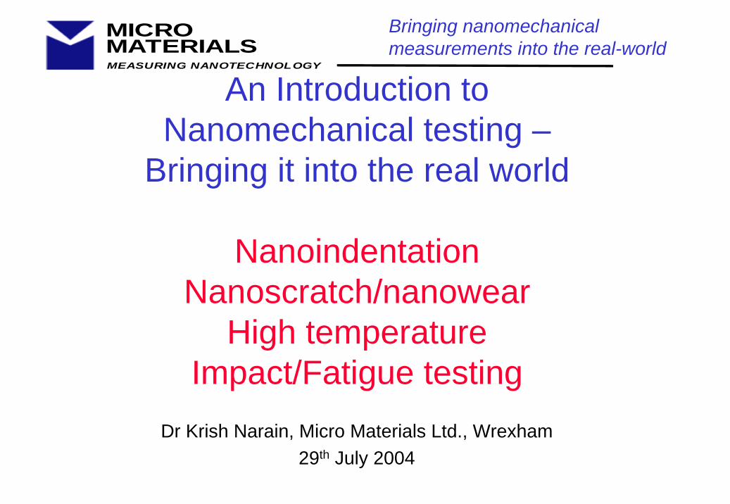
An Introduction to Nanomechanical testing –
Bringing it into the real world
NanoindentationNanoscratch/nanowear
High temperatureImpact/Fatigue testing
Dr Krish Narain, Micro Materials Ltd., Wrexham29th July 2004
Bringing nanomechanicalmeasurements into the real-world
MEASURING NANOTECHNOLOGY
MICROMATERIALS
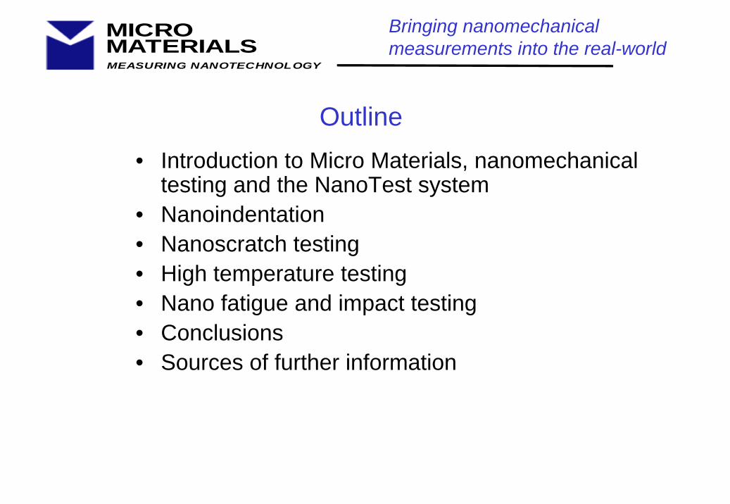
Outline• Introduction to Micro Materials, nanomechanical
testing and the NanoTest system• Nanoindentation• Nanoscratch testing• High temperature testing• Nano fatigue and impact testing• Conclusions• Sources of further information
Bringing nanomechanicalmeasurements into the real-world
MEASURING NANOTECHNOLOGY
MICROMATERIALS
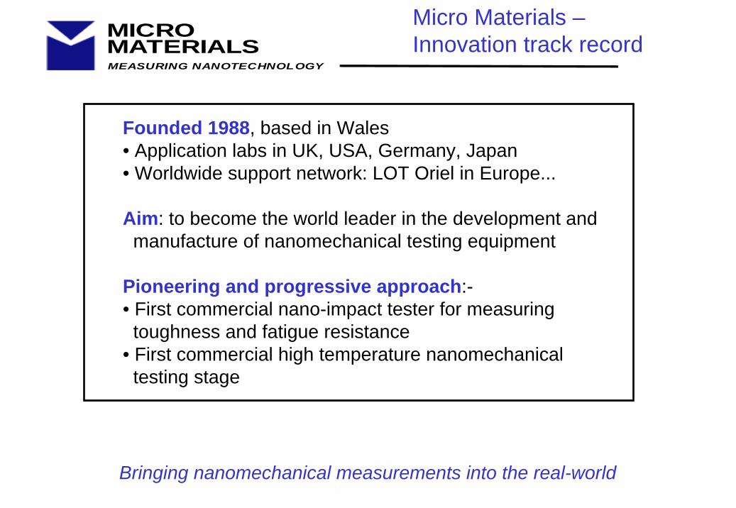
Founded 1988, based in Wales• Application labs in UK, USA, Germany, Japan• Worldwide support network: LOT Oriel in Europe...
Aim: to become the world leader in the development and manufacture of nanomechanical testing equipment
Pioneering and progressive approach:-• First commercial nano-impact tester for measuringtoughness and fatigue resistance
• First commercial high temperature nanomechanical testing stage
Micro Materials –Innovation track record
Bringing nanomechanical measurements into the real-world

MEASURING NANOTECHNOLOGY
MICROMATERIALS
Micro Materials is based in Wrexham
Where is Wrexham?It is in Wales, to the west of
England.What is Wales famous for?Sheep, coal-mines (now all
shut), leeks and rugby - and the NanoTest
MEASURING NANOTECHNOLOGY
MICROMATERIALS
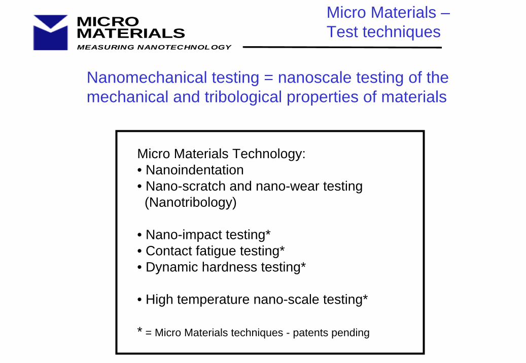
Micro Materials Technology:• Nanoindentation • Nano-scratch and nano-wear testing (Nanotribology)
• Nano-impact testing*• Contact fatigue testing*• Dynamic hardness testing*
• High temperature nano-scale testing*
* = Micro Materials techniques - patents pending
Nanomechanical testing = nanoscale testing of the mechanical and tribological properties of materials
Micro Materials –Test techniques
MEASURING NANOTECHNOLOGY
MICROMATERIALS
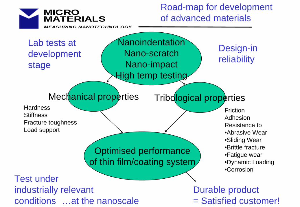
Optimised performanceof thin film/coating system
Road-map for development of advanced materials
Mechanical propertiesHardnessStiffnessFracture toughnessLoad support
Tribological propertiesFrictionAdhesionResistance to•Abrasive Wear•Sliding Wear•Brittle fracture•Fatigue wear•Dynamic Loading•Corrosion
Design-in reliability
…at the nanoscaleDurable product= Satisfied customer!
NanoindentationNano-scratchNano-impact
High temp testing
Lab tests at development stage
Test under industrially relevant conditions
MEASURING NANOTECHNOLOGY
MICROMATERIALS
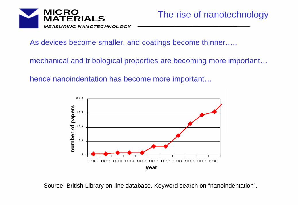
Source: British Library on-line database. Keyword search on “nanoindentation”.
As devices become smaller, and coatings become thinner…..
mechanical and tribological properties are becoming more important…
hence nanoindentation has become more important…
The rise of nanotechnology
MEASURING NANOTECHNOLOGY
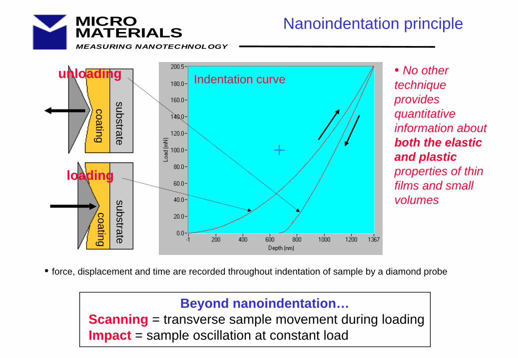
MICROMATERIALS Nanoindentation principle
loading
unloading
• force, displacement and time are recorded throughout indentation of sample by a diamond probe
Scanning = transverse sample movement during loadingImpact = sample oscillation at constant load
Beyond nanoindentation…
• No other technique provides quantitative information about both the elastic and plasticproperties of thin films and small volumes
Indentation curve
coatingcoating
substratesubstrate
MEASURING NANOTECHNOLOGY
MICROMATERIALS Viscoelastic Effects during Indentation
0
50
100
150
200
250
300
350
0 20 40 60 80 100
Cre
ep d
ispl
acem
ent (
nm)
Hold time (s)
Steel
Aluminum
Polyester
Epoxy
0
2
4
6
8
10
12
14
16
0 500 1000 1500 2000 2500
1 mN/s0.1 mN/s0.001 mN/s
Load
(mN
)Depth (nm)
Hold time = 100 sec
Data: Courtesy Dr Raman Singh, SUNY Stonybrook
Creep effects as a function ofloading rate
Creep at constant load
MEASURING NANOTECHNOLOGY
MICROMATERIALS
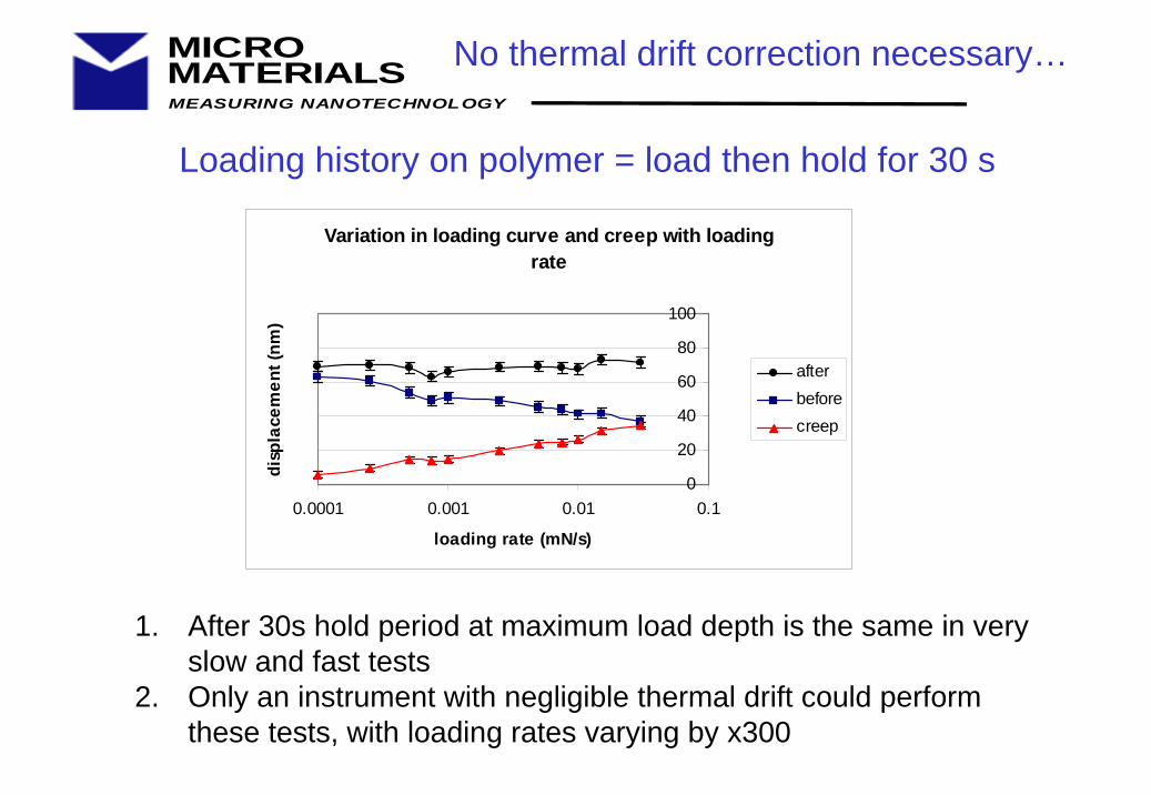
Variation in loading curve and creep with loading rate
0
20
40
60
80
100
0.0001 0.001 0.01 0.1
loading rate (mN/s)
disp
lace
men
t (nm
)
afterbeforecreep
1. After 30s hold period at maximum load depth is the same in very slow and fast tests
2. Only an instrument with negligible thermal drift could perform these tests, with loading rates varying by x300
Loading history on polymer = load then hold for 30 s
No thermal drift correction necessary…
MEASURING NANOTECHNOLOGY
MICROMATERIALS
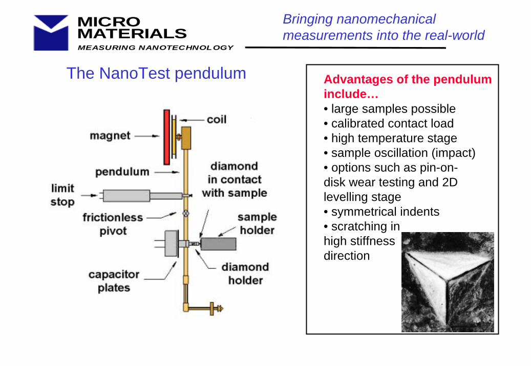
The NanoTest pendulum Advantages of the pendulum include…• large samples possible• calibrated contact load• high temperature stage• sample oscillation (impact)• options such as pin-on-disk wear testing and 2D levelling stage• symmetrical indents• scratching inhigh stiffnessdirection
Bringing nanomechanicalmeasurements into the real-world
MEASURING NANOTECHNOLOGY
MICROMATERIALS
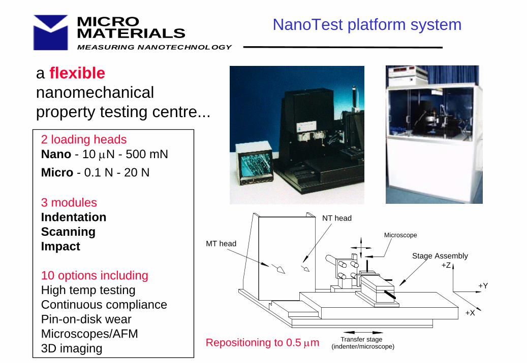
a flexiblenanomechanicalproperty testing centre...2 loading headsNano - 10 µN - 500 mNMicro - 0.1 N - 20 N
3 modulesIndentationScanningImpact
10 options includingHigh temp testingContinuous compliancePin-on-disk wearMicroscopes/AFM3D imaging
NanoTest platform system
Microscope
Transfer stage (indenter/microscope)
MT head
NT head
Stage Assembly+Z
+Y
+X
Repositioning to 0.5 µm
MEASURING NANOTECHNOLOGY
MICROMATERIALS
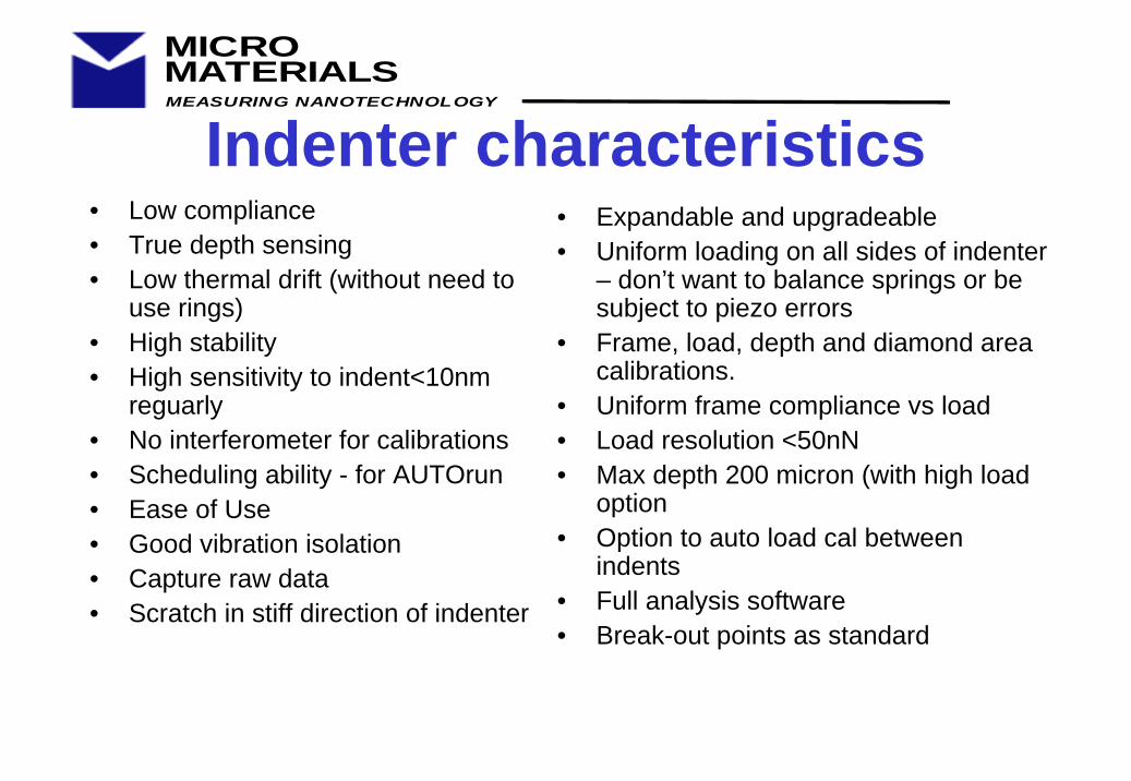
Indenter characteristics• Low compliance• True depth sensing• Low thermal drift (without need to
use rings)• High stability• High sensitivity to indent<10nm
reguarly• No interferometer for calibrations• Scheduling ability - for AUTOrun• Ease of Use• Good vibration isolation• Capture raw data• Scratch in stiff direction of indenter
• Expandable and upgradeable• Uniform loading on all sides of indenter
– don’t want to balance springs or be subject to piezo errors
• Frame, load, depth and diamond area calibrations.
• Uniform frame compliance vs load• Load resolution <50nN• Max depth 200 micron (with high load
option• Option to auto load cal between
indents • Full analysis software• Break-out points as standard
MEASURING NANOTECHNOLOGY
MICROMATERIALS
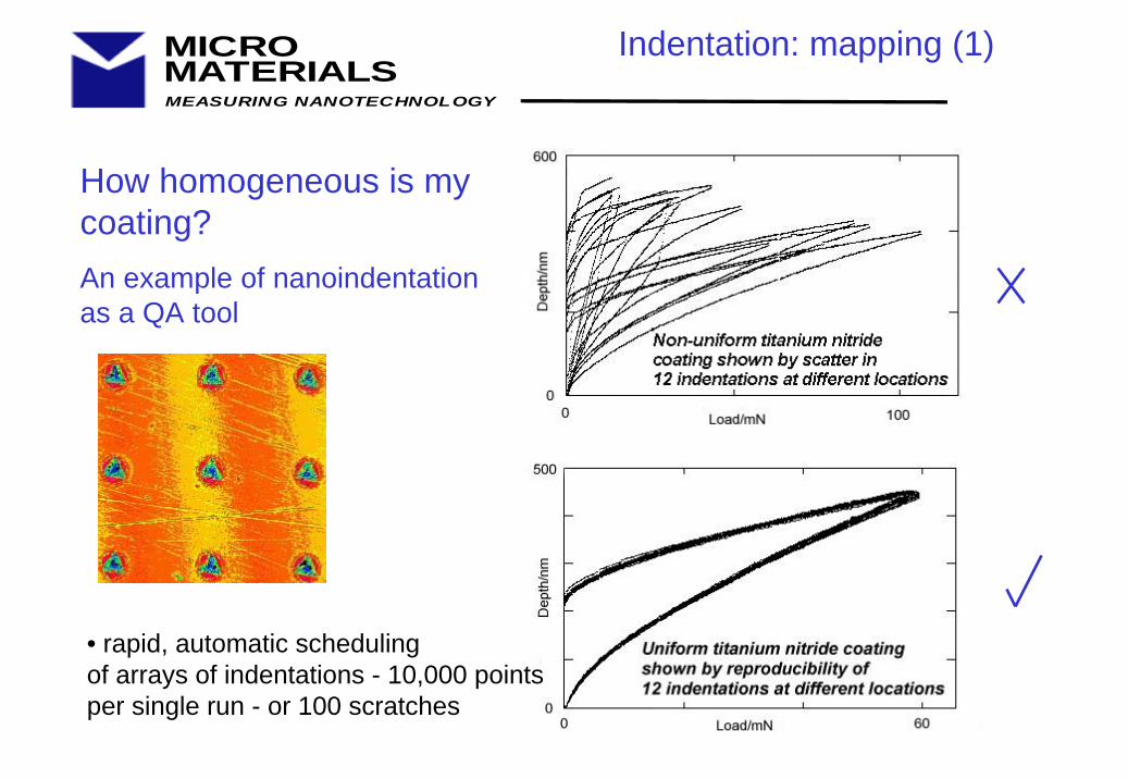
How homogeneous is mycoating?An example of nanoindentation as a QA tool
• rapid, automatic schedulingof arrays of indentations - 10,000 pointsper single run - or 100 scratches
Indentation: mapping (1)
MEASURING NANOTECHNOLOGY
MICROMATERIALS
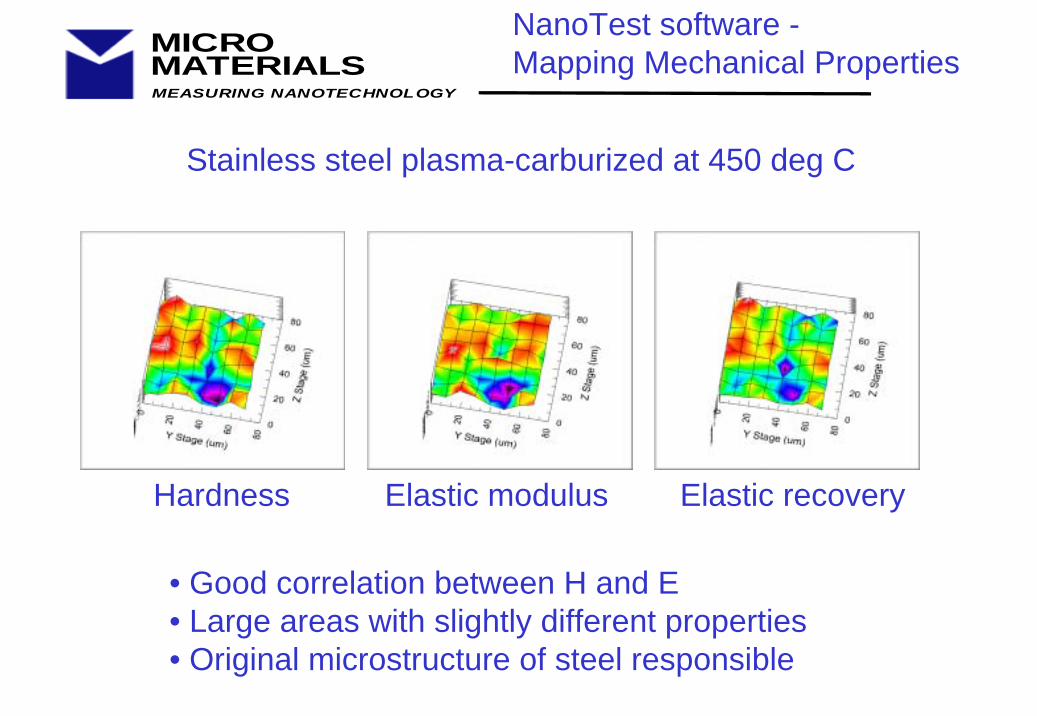
Stainless steel plasma-carburized at 450 deg C
Elastic modulusHardness
• Good correlation between H and E• Large areas with slightly different properties• Original microstructure of steel responsible
Elastic recovery
NanoTest software -Mapping Mechanical Properties
MEASURING NANOTECHNOLOGY
MICROMATERIALS
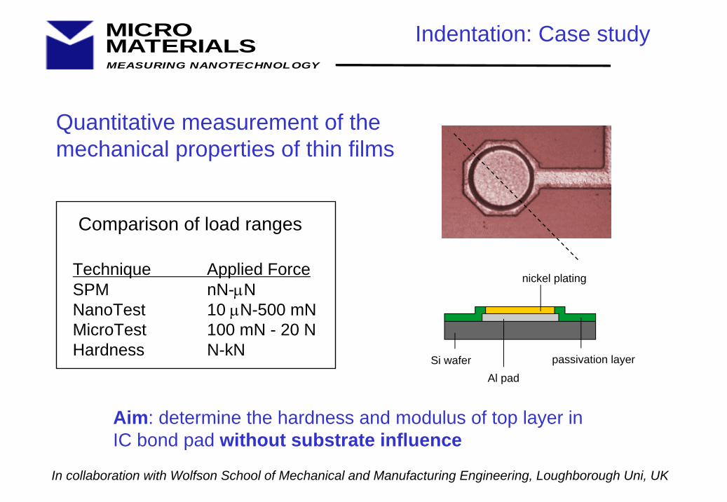
nickel plating
Al pad
passivation layerSi wafer
Quantitative measurement of themechanical properties of thin films
Aim: determine the hardness and modulus of top layer in IC bond pad without substrate influence
Technique Applied ForceSPM nN-µNNanoTest 10 µN-500 mNMicroTest 100 mN - 20 NHardness N-kN
Comparison of load ranges
Indentation: Case study
In collaboration with Wolfson School of Mechanical and Manufacturing Engineering, Loughborough Uni, UK
MEASURING NANOTECHNOLOGY
MICROMATERIALS
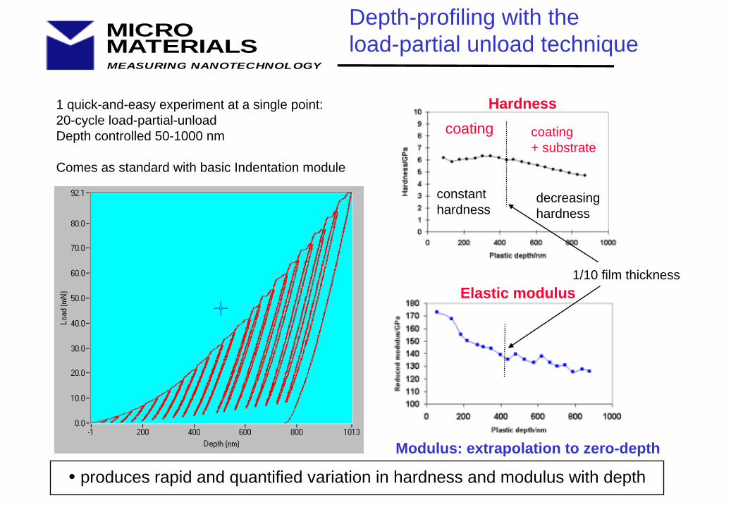
Depth-profiling with the load-partial unload technique
1 quick-and-easy experiment at a single point:20-cycle load-partial-unloadDepth controlled 50-1000 nm
Comes as standard with basic Indentation module
• produces rapid and quantified variation in hardness and modulus with depth
constanthardness
decreasinghardness
coating coating + substrate
Hardness
Elastic modulus
Modulus: extrapolation to zero-depth
1/10 film thickness
MEASURING NANOTECHNOLOGY
MICROMATERIALS
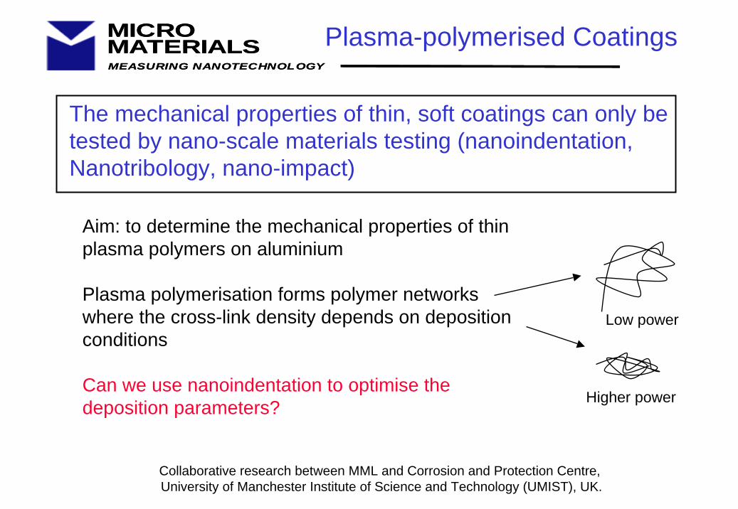
Aim: to determine the mechanical properties of thin plasma polymers on aluminium
Plasma polymerisation forms polymer networks where the cross-link density depends on deposition conditions
Can we use nanoindentation to optimise the deposition parameters?
Collaborative research between MML and Corrosion and Protection Centre, University of Manchester Institute of Science and Technology (UMIST), UK.
MEASURING NANOTECHNOLOGY
MICROMATERIALS
Low power
Higher power
The mechanical properties of thin, soft coatings can only be tested by nano-scale materials testing (nanoindentation, Nanotribology, nano-impact)
Plasma-polymerised Coatings

MEASURING NANOTECHNOLOGY
MICROMATERIALS
Depth profiling with the load-partial-unload technique
100 W
25 W
100 W
25 W
20 cycle load-partial-unload experiment – takes 30 mins
Plasma-polymers deposited at 100 W and 25 W power…
MEASURING NANOTECHNOLOGY
MICROMATERIALSMEASURING NANOTECHNOLOGY
MICROMATERIALS
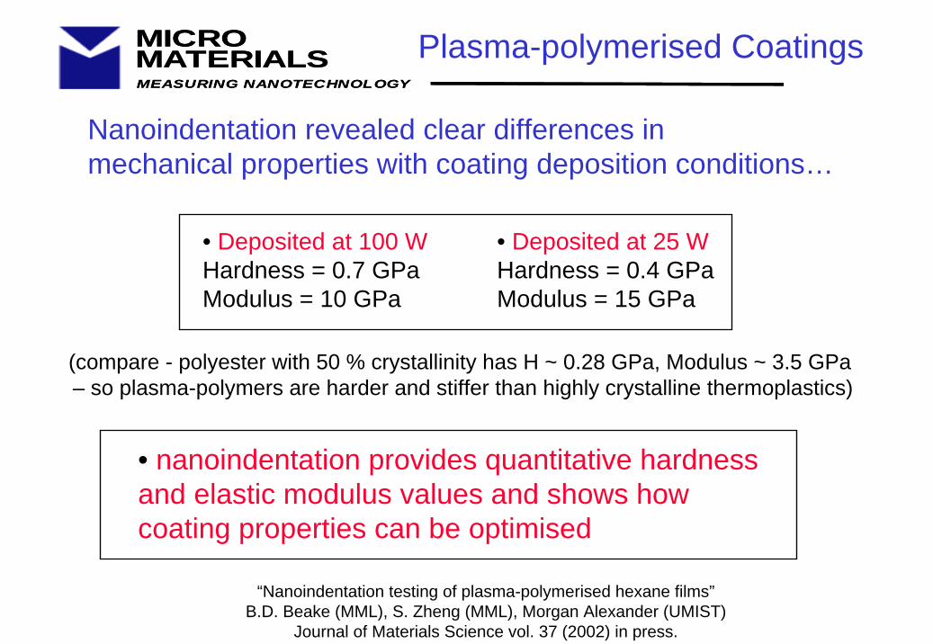
• Deposited at 100 WHardness = 0.7 GPaModulus = 10 GPa
• Deposited at 25 WHardness = 0.4 GPaModulus = 15 GPa
Nanoindentation revealed clear differences in mechanical properties with coating deposition conditions…
(compare - polyester with 50 % crystallinity has H ~ 0.28 GPa, Modulus ~ 3.5 GPa – so plasma-polymers are harder and stiffer than highly crystalline thermoplastics)
• nanoindentation provides quantitative hardness and elastic modulus values and shows how coating properties can be optimised
“Nanoindentation testing of plasma-polymerised hexane films”B.D. Beake (MML), S. Zheng (MML), Morgan Alexander (UMIST)
Journal of Materials Science vol. 37 (2002) in press.
Plasma-polymerised Coatings
MEASURING NANOTECHNOLOGY
MICROMATERIALS
0
100
200
300
400
0
50
100
150
200
250
300
350
400
450
0255075100
125
150
175
200
225
250
275
300
325
350
375
y
z
125-150 150-175
175-200 200-225
225-250 250-275
275-300 300-325
325-350 350-375
0
100
200
300
400
0
50
100
150
200
250
300
350
400
450
00.
250.5
0.751
1.251.5
1.752
2.252.5
2.753
3.253.5
3.754
4.254.5
4.755
5.255.5
5.75
y
z
5.5-5.75
5.25-5.5
5-5.25
4.75-5
4.5-4.75
4.25-4.5
4-4.25
3.75-4
3.5-3.75
3.25-3.5
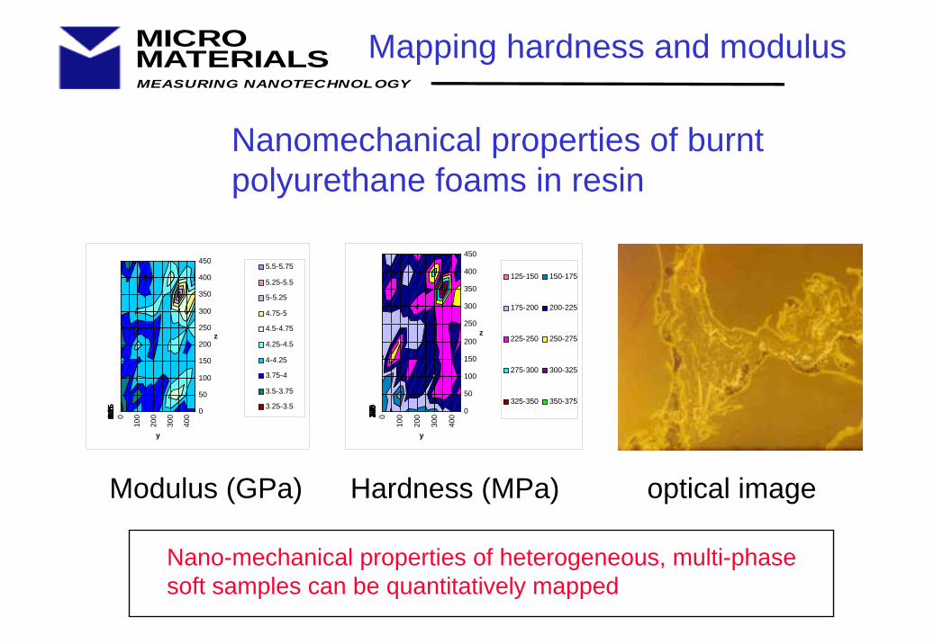
Nanomechanical properties of burnt polyurethane foams in resin
Modulus (GPa) Hardness (MPa) optical image
Nano-mechanical properties of heterogeneous, multi-phase soft samples can be quantitatively mapped
Mapping hardness and modulus

MEASURING NANOTECHNOLOGY
MICROMATERIALS
Coil
Ceramic
Capacitor plates Indenter
MicroTest pendulum
MEASURING NANOTECHNOLOGY
MICROMATERIALS
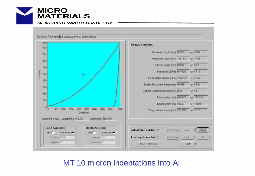
MT 10 micron indentations into Al
MEASURING NANOTECHNOLOGY
MICROMATERIALS
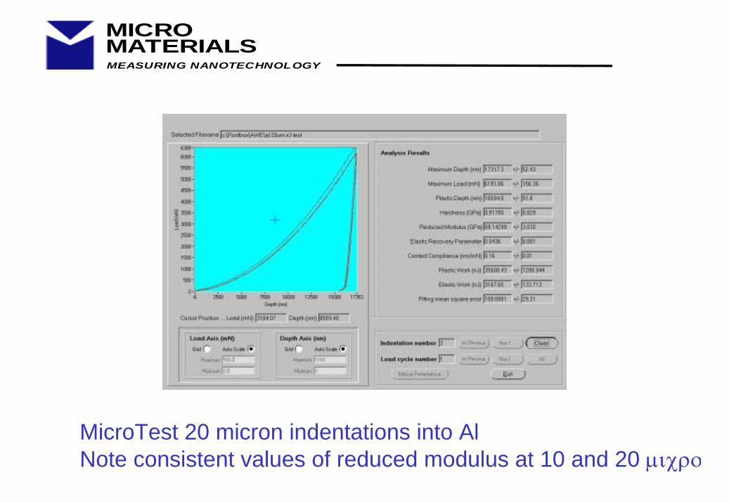
MicroTest 20 micron indentations into AlNote consistent values of reduced modulus at 10 and 20 µιχρο

MEASURING NANOTECHNOLOGY
MICROMATERIALS
MicroTest 6.4N indentations into WReduced modulus lit value = 320 GPaIs equivalent to lit value of Young’s modulus of 410Despite poor sample quality (see loading curves) still v. accurate
MEASURING NANOTECHNOLOGY
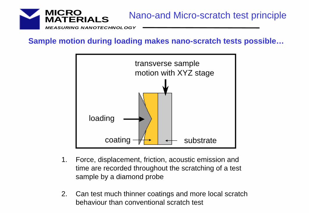
MICROMATERIALS Nano-and Micro-scratch test principle
loading
1. Force, displacement, friction, acoustic emission and time are recorded throughout the scratching of a test sample by a diamond probe
2. Can test much thinner coatings and more local scratch behaviour than conventional scratch test
coating substrate
Sample motion during loading makes nano-scratch tests possible…
transverse samplemotion with XYZ stage
MEASURING NANOTECHNOLOGY
MICROMATERIALS
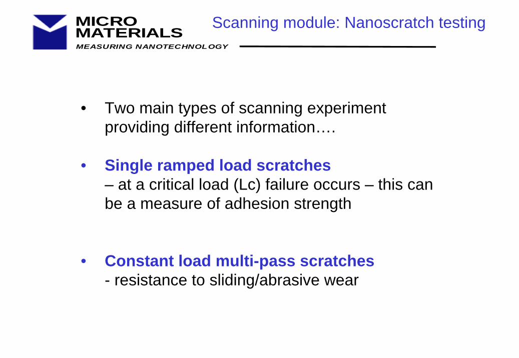
• Two main types of scanning experiment providing different information….
• Single ramped load scratches– at a critical load (Lc) failure occurs – this can be a measure of adhesion strength
• Constant load multi-pass scratches- resistance to sliding/abrasive wear
Scanning module: Nanoscratch testing
MEASURING NANOTECHNOLOGY
MICROMATERIALS
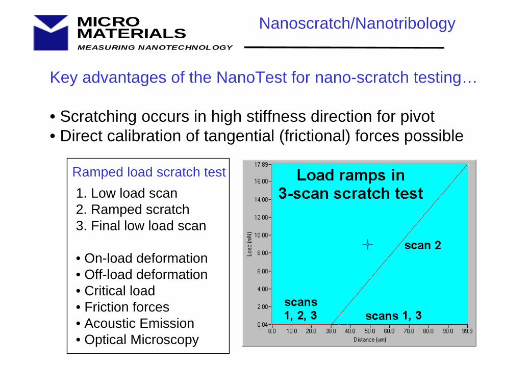
Ramped load scratch test1. Low load scan2. Ramped scratch3. Final low load scan
• On-load deformation• Off-load deformation• Critical load• Friction forces• Acoustic Emission• Optical Microscopy
Nanoscratch/Nanotribology
Key advantages of the NanoTest for nano-scratch testing…
• Scratching occurs in high stiffness direction for pivot• Direct calibration of tangential (frictional) forces possible
MEASURING NANOTECHNOLOGY
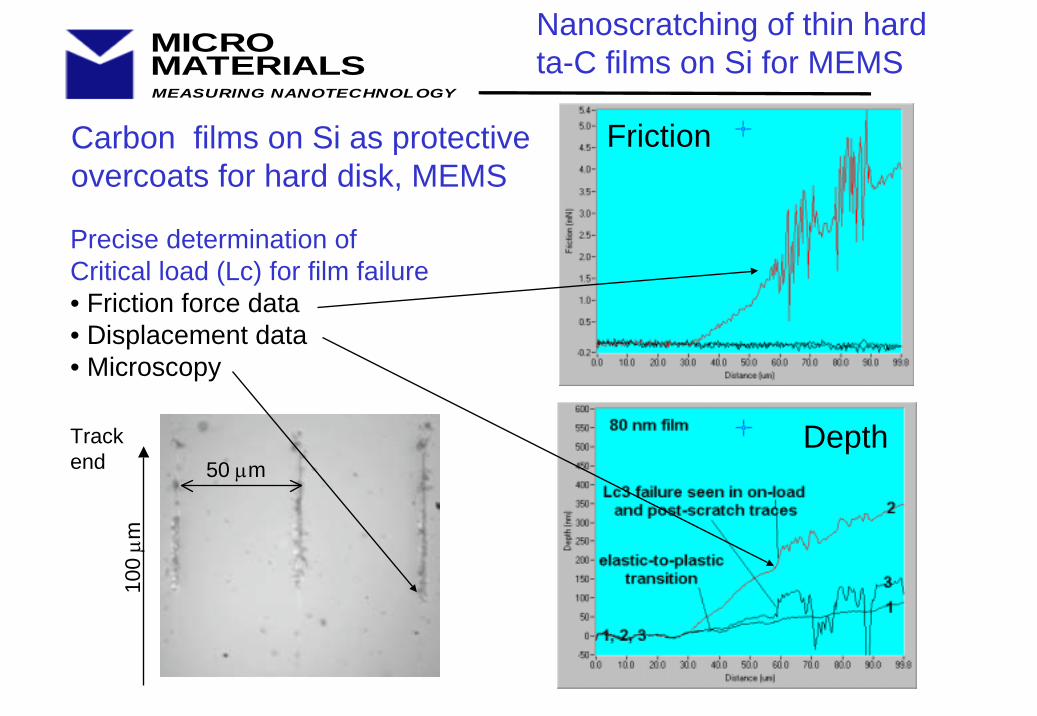
MICROMATERIALS
50 µm
100 µm
Precise determination of Critical load (Lc) for film failure • Friction force data• Displacement data• Microscopy
Carbon films on Si as protective overcoats for hard disk, MEMS
Track end
Friction
Depth
Nanoscratching of thin hard ta-C films on Si for MEMS
MEASURING NANOTECHNOLOGY
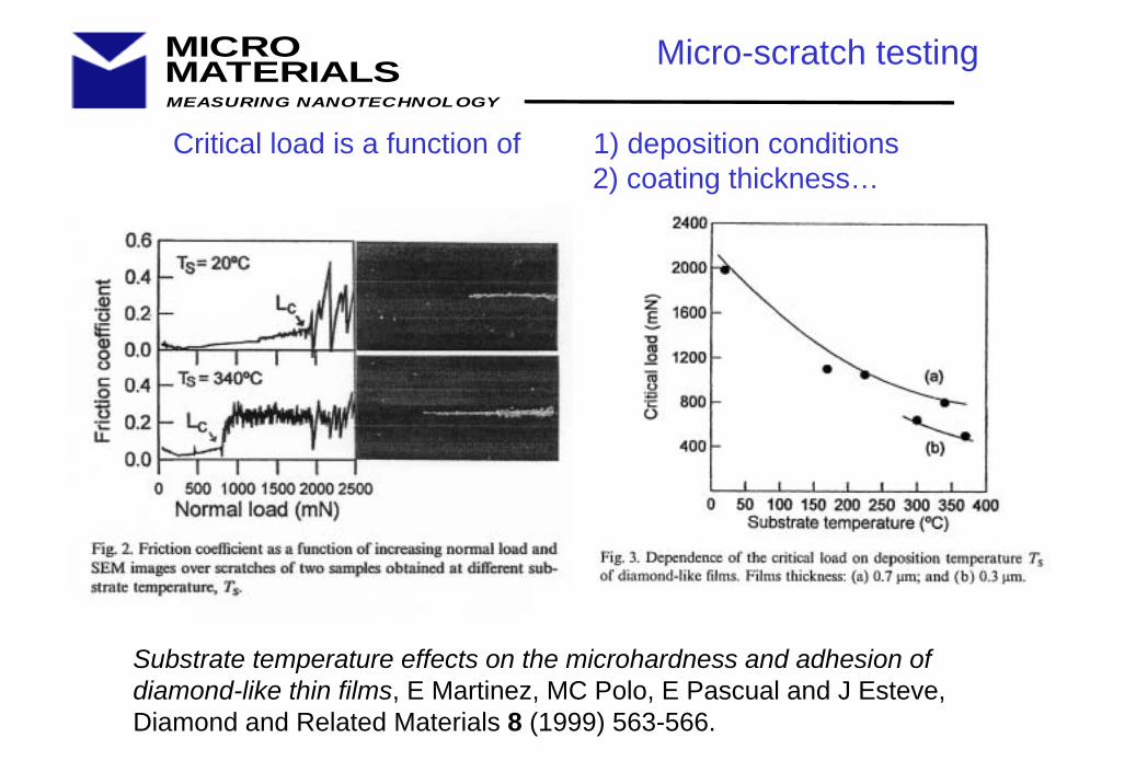
MICROMATERIALS Micro-scratch testing
Substrate temperature effects on the microhardness and adhesion of diamond-like thin films, E Martinez, MC Polo, E Pascual and J Esteve, Diamond and Related Materials 8 (1999) 563-566.
Critical load is a function of 1) deposition conditions2) coating thickness…
MEASURING NANOTECHNOLOGY
MICROMATERIALS
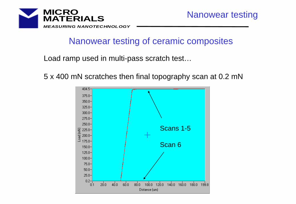
Load ramp used in multi-pass scratch test…
5 x 400 mN scratches then final topography scan at 0.2 mN
Nanowear testing
Nanowear testing of ceramic composites
Scans 1-5
Scan 6

MEASURING NANOTECHNOLOGY
MICROMATERIALS
• Clear differences in nano-/micro- scale wear resistance between different ceramic composites• Correlates to nanoindentation hardness
Zirconia/Mullite Alumina/Zirconia Zirconia/Alumina
~1 µm wear depth ~2 µm wear depth ~3 µm wear depth
Nanowear testing
Nanowear testing of ceramic composites

MEASURING NANOTECHNOLOGY
MICROMATERIALS
2 different PET samples -clear differences in nano-scratching wearwith processing history...
Biaxially drawn PET film - 50% crystalline
dplast
dtotal
dplast
dtotal
• extent of ploughing
• differences inelastic recovery (dp/dt)
Uniaxially drawn PET film ~ 30% crystalline
Evaluate slidingwear resistance ofdifferent coatingformulations
Nanotribology
BD Beake (MML) and GJ Leggett (UMIST), Polymer 2002, 43, 319-327.

MEASURING NANOTECHNOLOGY
MICROMATERIALS
Nanoindentation – mechanical properties (hardness, modulus, creep)Nanoscratch – tribological properties (resistance to abrasive/sliding wear)
Conventional nanoscale testing techniques provide part of the solution…
But…
• All material properties are temperature-dependent• Materials often fail by fatigue not overload
MEASURING NANOTECHNOLOGY
MICROMATERIALS
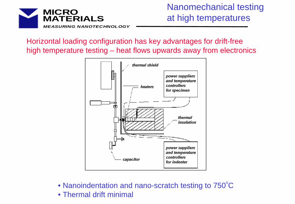
Nanomechanical testing at high temperatures
• Nanoindentation and nano-scratch testing to 750oC• Thermal drift minimal
Horizontal loading configuration has key advantages for drift-free high temperature testing – heat flows upwards away from electronics
MEASURING NANOTECHNOLOGY
MICROMATERIALS
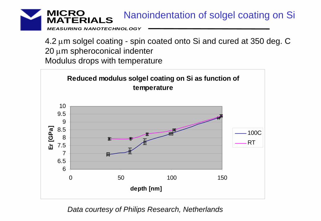
Reduced modulus solgel coating on Si as function of temperature
66.5
77.5
88.5
99.510
0 50 100 150
depth [nm]
Er [G
Pa]
100CRT
Nanoindentation of solgel coating on Si
4.2 µm solgel coating - spin coated onto Si and cured at 350 deg. C20 µm spheroconical indenter Modulus drops with temperature
Data courtesy of Philips Research, Netherlands
MEASURING NANOTECHNOLOGY
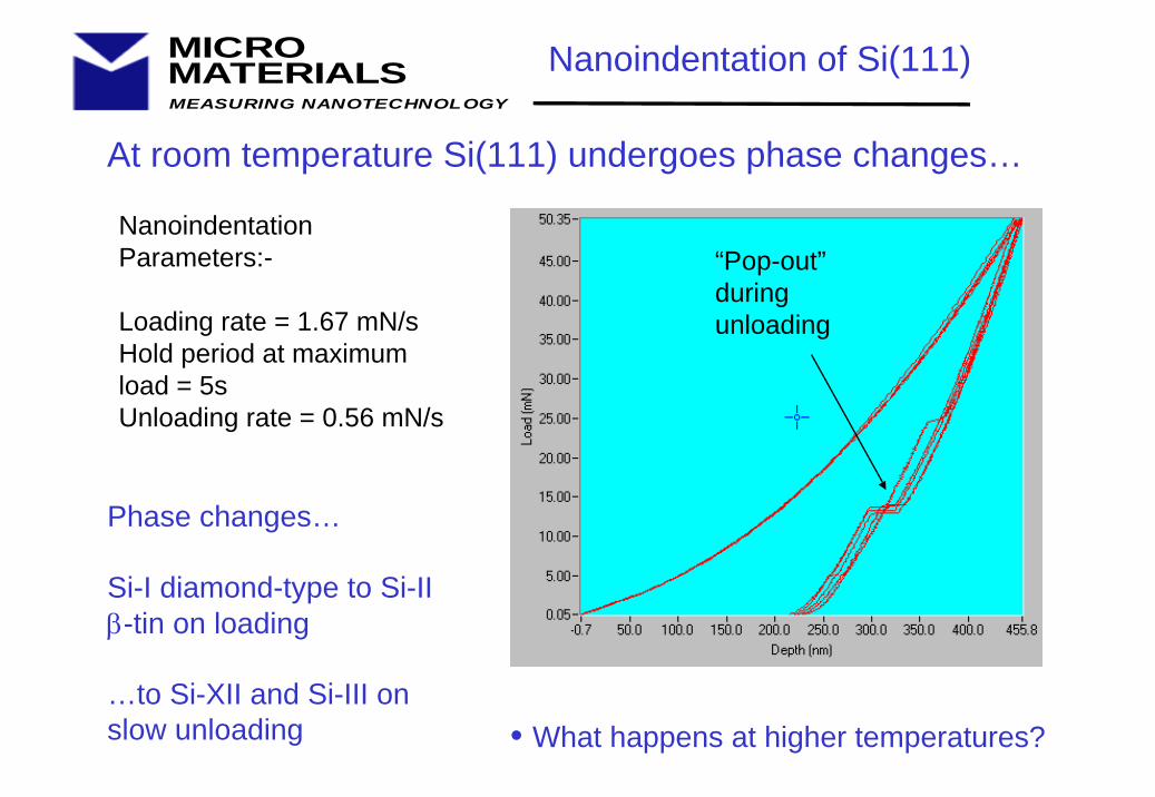
MICROMATERIALS Nanoindentation of Si(111)
At room temperature Si(111) undergoes phase changes…
NanoindentationParameters:-
Loading rate = 1.67 mN/sHold period at maximum load = 5sUnloading rate = 0.56 mN/s
• What happens at higher temperatures?
“Pop-out”during unloading
Phase changes…
Si-I diamond-type to Si-II β-tin on loading
…to Si-XII and Si-III on slow unloading
MEASURING NANOTECHNOLOGY
MICROMATERIALS
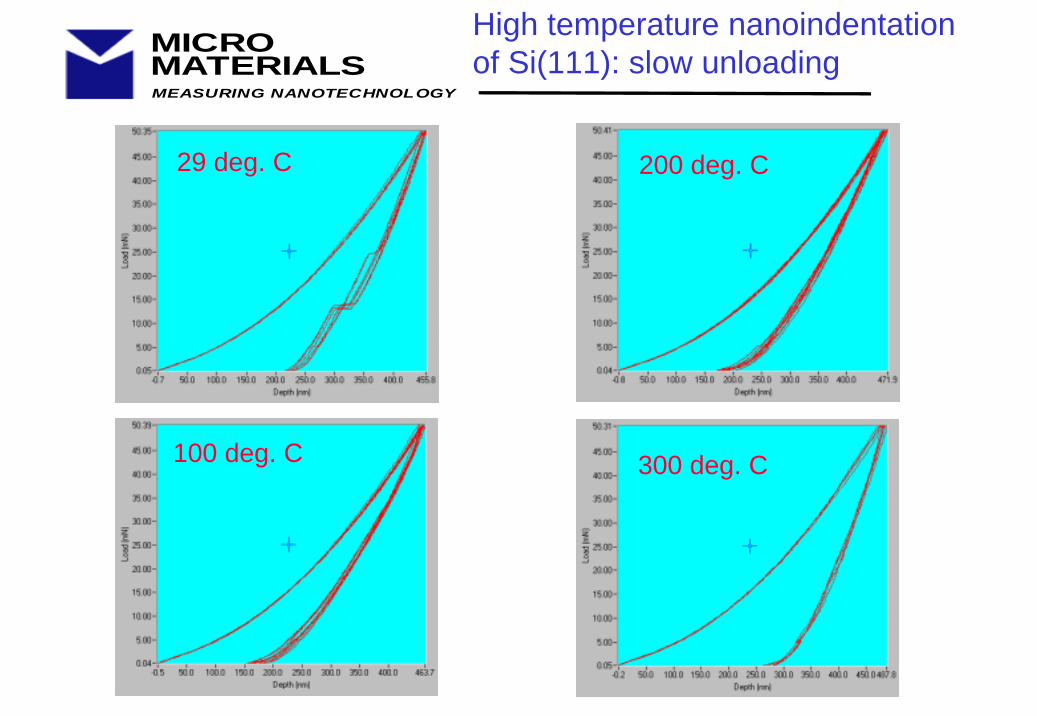
High temperature nanoindentation of Si(111): slow unloading
100 deg. C 300 deg. C
200 deg. C29 deg. C
MEASURING NANOTECHNOLOGY
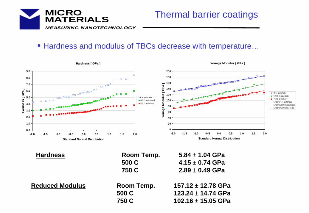
MICROMATERIALS Thermal barrier coatings
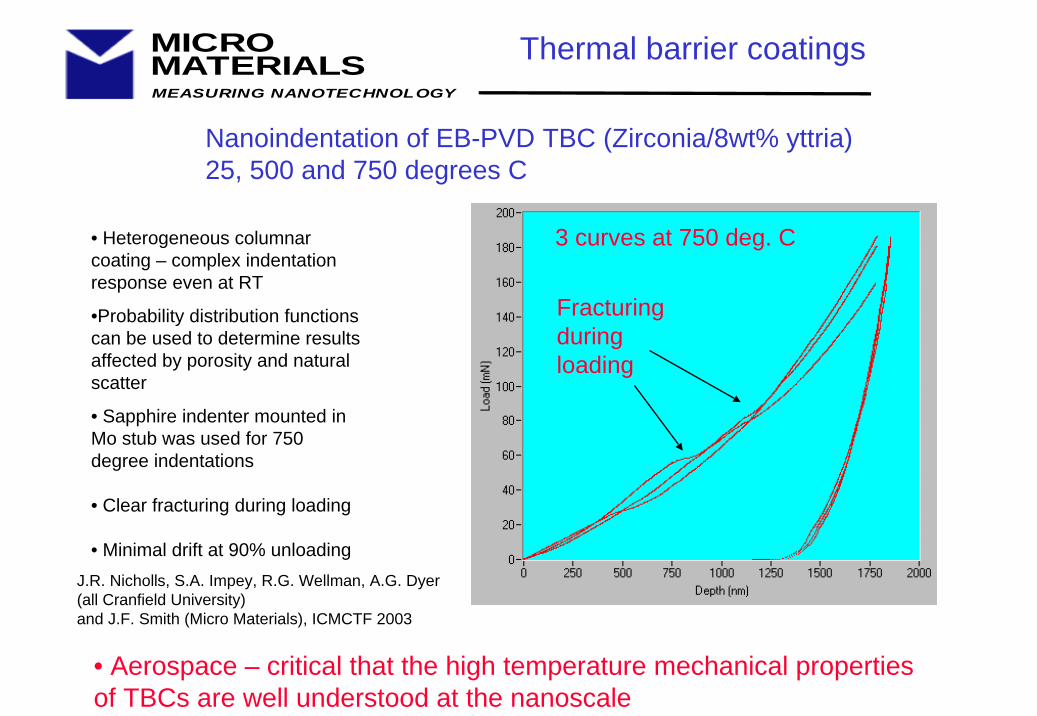
• Heterogeneous columnar coating – complex indentation response even at RT
•Probability distribution functions can be used to determine results affected by porosity and natural scatter
• Sapphire indenter mounted in Mo stub was used for 750 degree indentations
• Clear fracturing during loading
• Minimal drift at 90% unloadingJ.R. Nicholls, S.A. Impey, R.G. Wellman, A.G. Dyer (all Cranfield University) and J.F. Smith (Micro Materials), ICMCTF 2003
Nanoindentation of EB-PVD TBC (Zirconia/8wt% yttria) 25, 500 and 750 degrees C
Fracturing during loading
3 curves at 750 deg. C
• Aerospace – critical that the high temperature mechanical properties of TBCs are well understood at the nanoscale
MEASURING NANOTECHNOLOGY
MICROMATERIALS
Reduced Modulus Room Temp. 157.12 ± 12.78 GPa500 C 123.24 ± 14.74 GPa750 C 102.16 ± 15.05 GPa
Youngs Modulus [ GPa ]
0
20
40
60
80
100
120
140
160
180
200
-2.0 -1.5 -1.0 -0.5 0.0 0.5 1.0 1.5 2.0
Standard Normal Distribution
Youn
gs M
odul
us [
GPa
]
R.T. (polished)500 C (calculated)750 C (polished)Linear (R.T. (polished))Linear (500 C (calculated))Linear (750 C (polished))
Hardness [ GPa ]
0.0
1.0
2.0
3.0
4.0
5.0
6.0
7.0
8.0
9.0
-2.0 -1.5 -1.0 -0.5 0.0 0.5 1.0 1.5 2.0
Standard Normal Distribution
Hard
ness
[ G
Pa ]
R.T. (polished)500 C (calculated)750 C (polished)
Hardness Room Temp. 5.84 ± 1.04 GPa500 C 4.15 ± 0.74 GPa750 C 2.89 ± 0.49 GPa
• Hardness and modulus of TBCs decrease with temperature…
Thermal barrier coatings
MEASURING NANOTECHNOLOGY
MICROMATERIALS Nano-impact testing
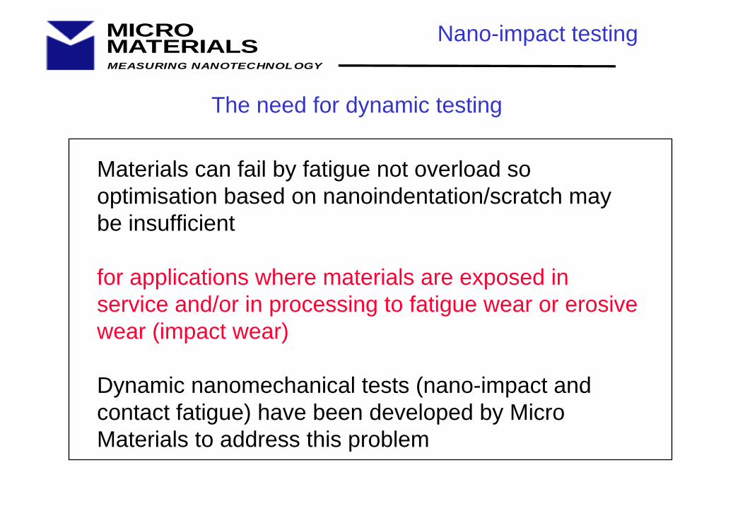
Materials can fail by fatigue not overload so optimisation based on nanoindentation/scratch may be insufficient
for applications where materials are exposed in service and/or in processing to fatigue wear or erosive wear (impact wear)
Dynamic nanomechanical tests (nano-impact and contact fatigue) have been developed by Micro Materials to address this problem
The need for dynamic testing
MEASURING NANOTECHNOLOGY
MICROMATERIALS
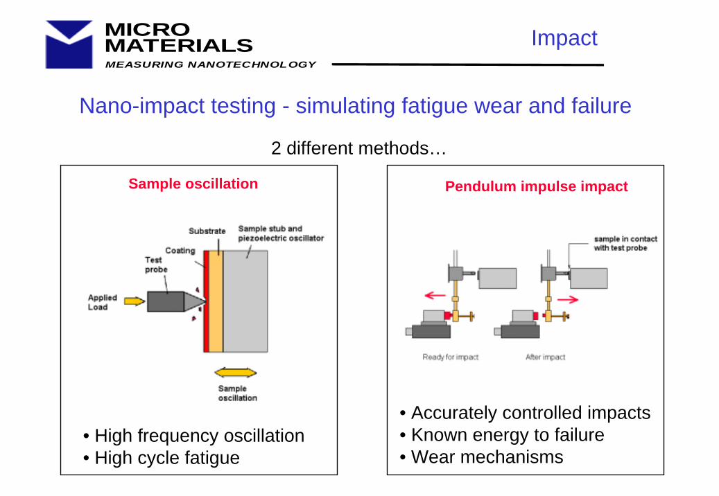
Nano-impact testing - simulating fatigue wear and failure
Impact
Sample oscillation
2 different methods…
• High frequency oscillation• High cycle fatigue
• Accurately controlled impacts• Known energy to failure• Wear mechanisms
Pendulum impulse impact
MEASURING NANOTECHNOLOGY
MICROMATERIALS
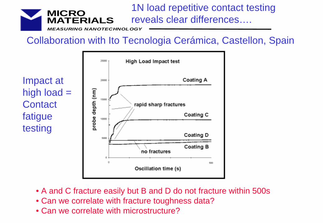
Impact at high load = Contact fatigue testing
• A and C fracture easily but B and D do not fracture within 500s• Can we correlate with fracture toughness data? • Can we correlate with microstructure?
1N load repetitive contact testing reveals clear differences….
Collaboration with Ito Tecnologia Cerámica, Castellon, Spain
MEASURING NANOTECHNOLOGY
MICROMATERIALS
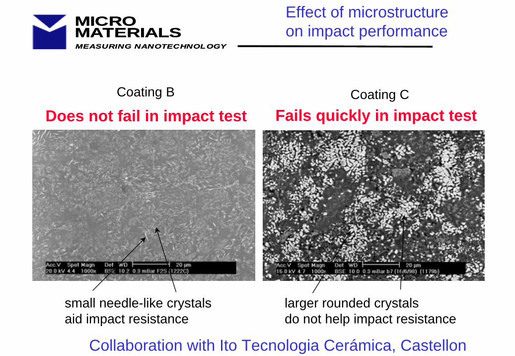
Coating B Coating C
Effect of microstructure on impact performance
small needle-like crystalsaid impact resistance
larger rounded crystalsdo not help impact resistance
MEASURING NANOTECHNOLOGY
MICROMATERIALS
Collaboration with Ito Tecnologia Cerámica, Castellon
Does not fail in impact test Fails quickly in impact test

MEASURING NANOTECHNOLOGY
MICROMATERIALS
Impact testing of ceramic coatings:comparison fracture toughness from SEM
• Hardness and Young’s Modulus did not vary• Scratch testing frustrated by high surface roughness
• Correlation with fracture toughness data from SEM…
• Impact resistant samples had high fracture toughness
• Time-to-failure • Change in Probe Depth
…measures of resistance to brittle fracture
“Micro-impact testing: a new technique for investigating fracture toughness” BD Beake (MML), Maria Jesus Ibanez Garcia (ITC Spain) and JF Smith (MML), Thin Solid Films 398-399 (2001) 438-443.
Low depth change = high fracture toughness
Collaboration with Ito Tecnologia Cerámica, Castellon
MEASURING NANOTECHNOLOGY
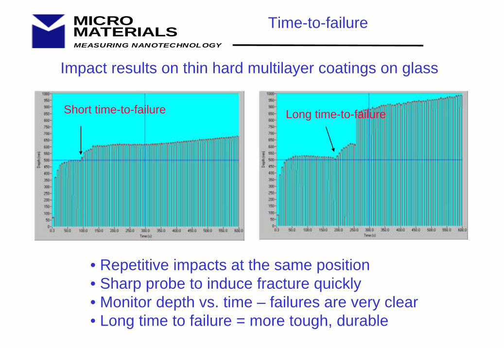
MICROMATERIALS Time-to-failure
Impact results on thin hard multilayer coatings on glass
• Repetitive impacts at the same position• Sharp probe to induce fracture quickly• Monitor depth vs. time – failures are very clear• Long time to failure = more tough, durable
Short time-to-failure Long time-to-failure
MEASURING NANOTECHNOLOGY
MICROMATERIALS
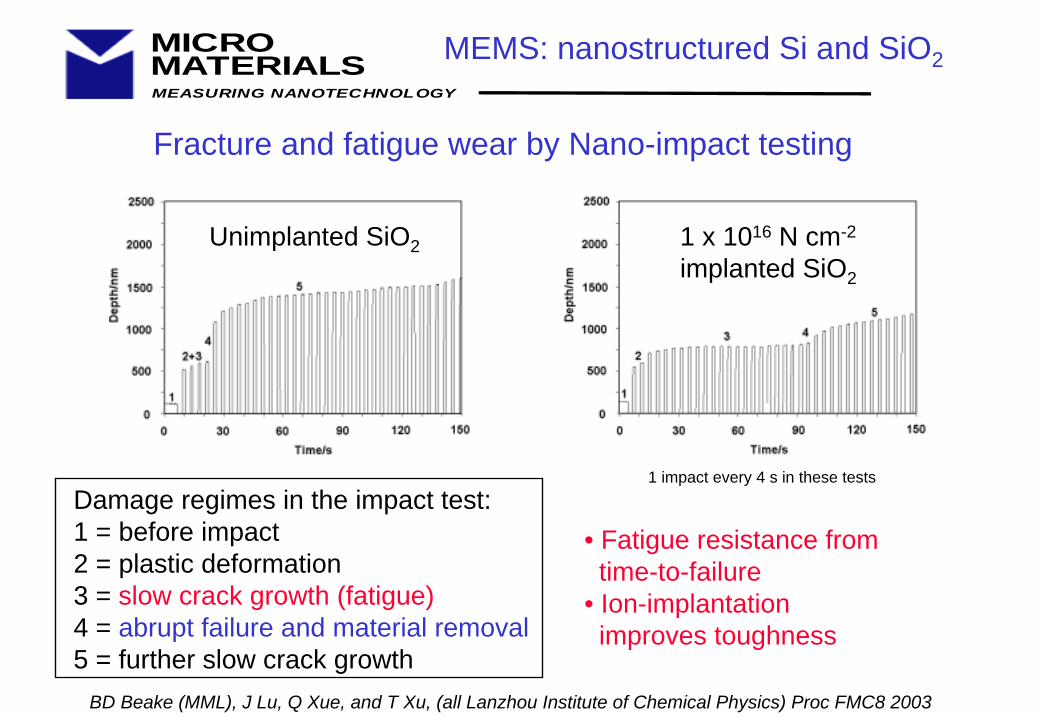
Unimplanted SiO2 1 x 10¹⁶ N cm-2
implanted SiO2
Damage regimes in the impact test:1 = before impact2 = plastic deformation3 = slow crack growth (fatigue)4 = abrupt failure and material removal5 = further slow crack growth
Fracture and fatigue wear by Nano-impact testing
MEMS: nanostructured Si and SiO2
• Fatigue resistance from time-to-failure
• Ion-implantationimproves toughness
BD Beake (MML), J Lu, Q Xue, and T Xu, (all Lanzhou Institute of Chemical Physics) Proc FMC8 2003
1 impact every 4 s in these tests

MEASURING NANOTECHNOLOGY
MICROMATERIALS
Damage mechanism in the impact test: before impact - plastic deformation - slow crack growth (fatigue) - abrupt failure and material removal - further slow crack growth
Fatigue and Fracture Wear of ta-C films
80 nmon Si
60 nmon Si
• time-to-first-failure to rank impact resistance• some plastic deformation of the substrate does occur (depth at failure)
5 nm
on Si
80 nmon Si

MEASURING NANOTECHNOLOGY
MICROMATERIALS
Diamond-like-carbon (DLC) has high hardness and low friction so it is being considered for many applications
But its fatigue properties have not been fully tested –this is particularly important asIt is prone to poor adhesionIt has been considered as an inert coating for biomedical devices
The NanoTest is being used to investigate the toughness and durability of DLC coatings to fatigue wear with the nano-impact facility…
DLC: is it tough enough for your application?
MEASURING NANOTECHNOLOGY
MICROMATERIALS
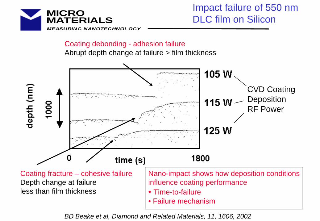
Impact failure of 550 nmDLC film on Silicon
Nano-impact shows how deposition conditionsinfluence coating performance• Time-to-failure• Failure mechanism
Coating debonding - adhesion failureAbrupt depth change at failure > film thickness
Coating fracture – cohesive failureDepth change at failure less than film thickness
CVD CoatingDepositionRF Power
BD Beake et al, Diamond and Related Materials, 11, 1606, 2002

MEASURING NANOTECHNOLOGY
MICROMATERIALS
Carbon coating on tool steel
• depth vs. time impact plot for multilayered carbon coating at 1mN• long time to failure
Coating failure
Multiple coating failures
DLC coating on tool steel
• depth vs. time impact plot for multilayered DLC coating at 1mN• short time-to-failure
Nano-impact testing reveals fatigue differences on coatings of the same hardness…
Impact – cube corner indenter
• Carbon coating much tougher than DLC
MEASURING NANOTECHNOLOGY
MICROMATERIALS
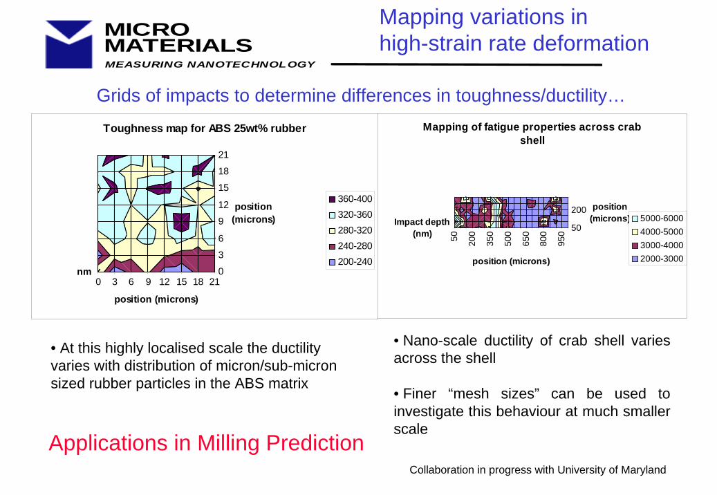
Mapping variations in high-strain rate deformation
50 200
350
500
650
800
950 50
200Impact depth
(nm)
position (microns)
position (microns)
Mapping of fatigue properties across crab shell
5000-60004000-50003000-40002000-3000
• Nano-scale ductility of crab shell varies across the shell
• Finer “mesh sizes” can be used to investigate this behaviour at much smaller scale
• At this highly localised scale the ductility varies with distribution of micron/sub-micron sized rubber particles in the ABS matrix
Grids of impacts to determine differences in toughness/ductility…
Collaboration in progress with University of Maryland
0 3 6 9 12 15 18 210
3
6
9
12
15
18
21
nm
position (microns)
position (microns)
Toughness map for ABS 25wt% rubber
360-400320-360280-320240-280200-240
Applications in Milling Prediction
MEASURING NANOTECHNOLOGY
MICROMATERIALS
Testing the viscoelastic properties of thin films and small volumes requires the ability to access a wide range of strain rates
The NanoTest system has far greater strain rate choice than other systems because
1. Ultra-slow loading, long creep tests etc, are possible due to excellent thermal stability (~0.001-0.01 nm/s)
2. Very high strain rates accessible – use nano-impact
Indentation: viscoelastic materials

MEASURING NANOTECHNOLOGY
MICROMATERIALS
Repetitive impact tests on brittle and ductile materials
• Focus on ability to absorb energy• More plastic deformation = more ductile• Less plastic deformation = less ductile
• Little plastic deformation before failure• Clear fracture event(s)• Time-to-failure characterises impact resistance
Less ductile
More ductile
Impact behaviour:brittle and ductile materials

MEASURING NANOTECHNOLOGY
MICROMATERIALS
Nano-impact of Rubber-modified ABS Polymer
Incorporation of 25 % rubber leads to greater depth change on repetitive impact at the same position
1 impact every 7 s; 5 mN impact force; spherical test probe
Nano-impact – ductile materials
MEASURING NANOTECHNOLOGY
MICROMATERIALS
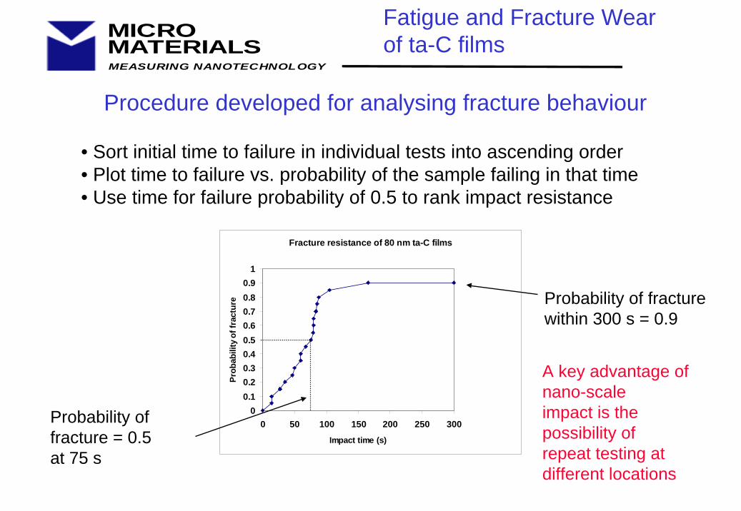
Fatigue and Fracture Wear of ta-C films
Procedure developed for analysing fracture behaviour
• Sort initial time to failure in individual tests into ascending order• Plot time to failure vs. probability of the sample failing in that time• Use time for failure probability of 0.5 to rank impact resistance
Fracture resistance of 80 nm ta-C films
00.10.20.30.40.50.60.70.80.9
1
0 50 100 150 200 250 300
Impact time (s)
Prob
abili
ty o
f fra
ctur
e Probability of fracturewithin 300 s = 0.9
Probability offracture = 0.5at 75 s
A key advantage ofnano-scaleimpact is thepossibility ofrepeat testing atdifferent locations
MEASURING NANOTECHNOLOGY
MICROMATERIALS
1 mN impact load
0
0.2
0.4
0.6
0.8
1
0 300 600 900 1200 1500 1800
time to failure (s)
Failu
re p
roba
bilit
y at
tim
e t
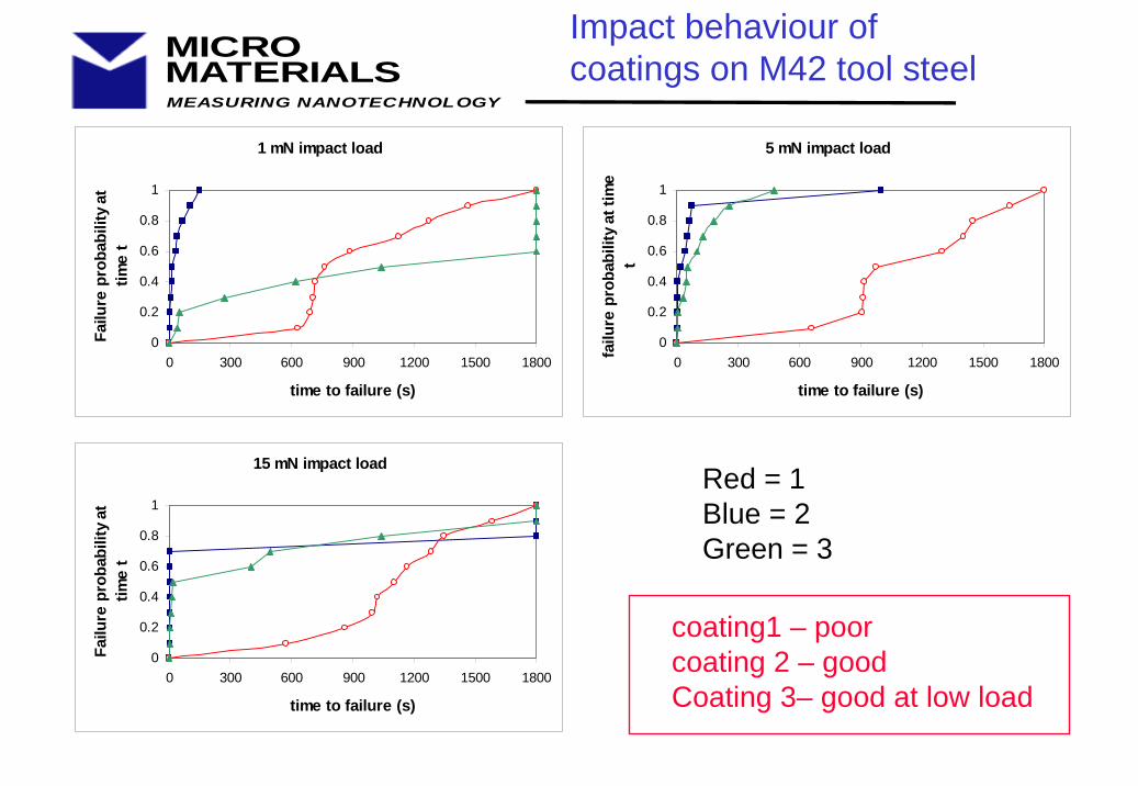
Impact behaviour of coatings on M42 tool steel
5 mN impact load
0
0.2
0.4
0.6
0.8
1
0 300 600 900 1200 1500 1800
time to failure (s)
failu
re p
roba
bilit
y at
tim
e t
15 mN impact load
0
0.2
0.4
0.6
0.8
1
0 300 600 900 1200 1500 1800
time to failure (s)
Failu
re p
roba
bilit
y at
tim
e t
Red = 1Blue = 2Green = 3
coating1 – poorcoating 2 – goodCoating 3– good at low load
MEASURING NANOTECHNOLOGY
MICROMATERIALS
Conclusions
1. Nanoindentation is fast becoming an essential tool in the optimisation of the mechanical and tribological properties of thin coated systems and advanced materials, for applications where hardness and stiffness are important.
2. The pendulum arrangement has key advantages for reliable scratchtesting. Scratching occurs in high stiffness direction for pivot and direct calibration of tangential (frictional) forces are possible.
3. Nano-scratch and nano-wear tests can accurately reveal differences in coating adhesion and wear resistance of coatings and bulk materials. This information can be used to aid materials processing and coating design.
Bringing nanomechanicalmeasurements into the real-world

MEASURING NANOTECHNOLOGY
MICROMATERIALS Conclusions
• New materials testing techniques – impact/fatigue testing and high temperature nanoindentation testing - have been developed to extend the capability of nanoindentation instruments
• Important since coatings are subjected to fatigue and extremes of temperature in service
• Development of these techniques is a notable advance enabling testing under contact conditions that more closely simulate those in service for the first time
• Test results can therefore be used with greater confidence to optimise the mechanical properties of coatings and surface treatments for specific applications
Bringing nanomechanical measurements into the real-world

MEASURING NANOTECHNOLOGY
MICROMATERIALS Acknowledgements
Further information
• Dr Jim Smith (Micro Materials)• Dr Stephen Goodes (Micro Materials)• Rob Parkinson (NEWI, UK)• Prof John Nicholls and co-workers (Cranfield Uni, UK)• Dr Jinjun Lu and co-workers (LSL, Lanzhou, China)• Dr Nathalie Renevier (Teer (now at UCLAN), UK)• Dr Rego and co-workers (MMU, UK)• Dr Daniel Lau (NTU, Singapore)• Philips Research (Eindhoven, Netherlands)
High temperature testingTCS Associate Rob Parkinson NEWI/Micro [email protected]
Nano-impact testingDr Nigel Jennett – Project Leader on NPL Project MPP2.2 – [email protected]

MEASURING NANOTECHNOLOGY
MICROMATERIALS
www.www.micromaterialsmicromaterials.co..co.ukuk• references• customer profiles• application notes
THANK YOU FOR LISTENING
HOW TO FIND FURTHER INFORMATION: