mcp specification - bdtic · mcp memory multi-chip package memory ... gnc/rasd dq15d dq16d dqs1d...
TRANSCRIPT
K524G2GACB-A050 MCP MEMORYhttp://www.BDTIC.com/SAMSUNG
MCP Specification
4Gb NAND Flash + 2Gb Mobile DDR
* Samsung Electronics reserves the right to change products or specification without notice.
INFORMATION IN THIS DOCUMENT IS PROVIDED IN RELATION TO SAMSUNG PRODUCTS, AND IS SUBJECT TO CHANGE WITHOUT NOTICE.
NOTHING IN THIS DOCUMENT SHALL BE CONSTRUED AS GRANTING ANY LICENSE, EXPRESS OR IMPLIED, BY ESTOPPEL OR OTHERWISE,
TO ANY INTELLECTUAL PROPERTY RIGHTS IN SAMSUNG PRODUCTS OR TECHNOLOGY. ALL INFORMATION IN THIS DOCUMENT IS PROVIDED
ON AS "AS IS" BASIS WITHOUT GUARANTEE OR WARRANTY OF ANY KIND.
1. For updates or additional information about Samsung products, contact your nearest Samsung office.
2. Samsung products are not intended for use in life support, critical care, medical, safety equipment, or similar applications where Product failure could result in loss of life or personal or physical harm, or any military or defense application, or any governmental procurement to which special terms or provisions may apply.
Revision 1.3November 2009
- 1 -

K524G2GACB-A050 MCP MEMORYhttp://www.BDTIC.com/SAMSUNG
Document TitleMulti-Chip Package MEMORY 4Gb (256M x16) NAND Flash Memory / 2Gb (64M x32) Mobile DDR SDRAM
1. Revision History
Note : For more detailed features and specifications including FAQ, please refer to Samsung’s web site. http://samsungelectronics.com/semiconductors/products/products_index.html
The attached datasheets are prepared and approved by SAMSUNG Electronics. SAMSUNG Electronics CO., LTD. reserve the right to change the specifications. SAMSUNG Electronics will evaluate and reply to your requests and questions about device. If you have any ques-tions, please contact the SAMSUNG branch office near you.
Revision No. History Draft Date Remark
0.0
1.0
1.1
1.2
1.3
Initial issue. - 4Gb NAND Flash W-die_ Ver 0.0 - 2Gb M-DDR SDRAM B-die_Ver 1.0
<NAND>_Ver 1.0 - Corrected Errata - ECC requirement updated - Final issue<DRAM>_Ver 1.2Ver 1.1 - Corrected errata.Ver 1.2 - Finalized.
<Common> - Finalized
<NAND>_Ver 1.011. ECC requirement updated
<NAND>_Ver 1.11. ECC requirement updated2. Chapter 3.10 : Updated note for Random data input<M-DDR>_Ver 1.3
<Common> - Added DDR333.
May. 8, 2009
Aug. 17, 2009
Sep. 03, 2009
Oct. 8, 2009
Nov. 26, 2009
Preliminary
Final
Final
Final
Final
Revision 1.3November 2009
- 2 -

K524G2GACB-A050 MCP MEMORYhttp://www.BDTIC.com/SAMSUNG
Multi-Chip Package MEMORY 4Gb (256M x16) NAND Flash Memory / 2Gb (64M x32) Mobile DDR SDRAM
2. FEATURES
SAMSUNG ELECTRONICS CO., LTD. reserves the right to change products and specifications without notice.
<Common>• Operating Temperature : -25°C ~ 85°C• Package : 137-ball FBGA Type - 10.5 x 13 x 1.2mmt, 0.8mm pitch
<NAND Flash>• Voltage Supply : 1.7V ~ 1.95V• Organization - Memory Cell Array : (256M + 8M) x 16bit for 4Gb (512M + 16M) x 16bit for 8Gb DDP - Data Register : (1K + 32) x 16bit• Automatic Program and Erase - Page Program : (1K + 32)Word - Block Erase : (64K + 2K)Word• Page Read Operation - Page Size : (1K + 32)Word - Random Read : 40µs(Max.) - Serial Access : 42ns(Min.) • Fast Write Cycle Time - Page Program time : 250µs(Typ.) - Block Erase Time : 2ms(Typ.)• Command/Address/Data Multiplexed I/O Port• Hardware Data - Program/Erase Lockout During Power Transitions• Reliable CMOS Floating-Gate Technology -Endurance : 100K Program/Erase Cycles with 1bit/256Word ECC for x16• Command Driven Operation• Unique ID for Copyright Protection
<Mobile DDR>• VDD/VDDQ = 1.8V/1.8V• Double-data-rate architecture; two data transfers per clock cycle• Bidirectional data strobe(DQS)• Four banks operation• Differential clock inputs(CK and CK)• MRS cycle with address key programs - CAS Latency ( 3 ) - Burst Length ( 2, 4, 8, 16 ) - Burst Type (Sequential & Interleave)• EMRS cycle with address key programs - Partial Array Self Refresh ( Full, 1/2, 1/4 Array ) - Output Driver Strength Control ( Full, 1/2, 1/4, 1/8, 3/4, 3/8, 5/8, 7/8 )• Internal Temperature Compensated Self Refresh• All inputs except data & DM are sampled at the positive going edge of
the system clock(CK).• Data I/O transactions on both edges of data strobe, DM for masking. • Edge aligned data output, center aligned data input.• No DLL; CK to DQS is not synchronized. • DM0 - DM3 for write masking only.• Auto refresh duty cycle - 7.8us• Clock stop capability
Note:1) CAS Latency
- DM is internally loaded to match DQ and DQS identically.
Operating FrequencyDDR333 DDR400
Speed @CL31) 166MHz 200MHz
Address configurationOrganization Bank Row Column
64Mx32 BA0,BA1 A0 - A13 A0 - A9
Revision 1.3November 2009
- 3 -
K524G2GACB-A050 MCP MEMORYhttp://www.BDTIC.com/SAMSUNG
3. GENERAL DESCRIPTIONThe K524G2GACB is a Multi Chip Package Memory which combines 4Gbit NAND Flash Memory an 2Gbit DDR synchronous high data rateDynamic RAM.
NAND cell provides the most cost-effective solution for the solid state application market. A program operation can be performed in typical250µs on the (1K+32)Word page and an erase operation can be performed in typical 2ms on a (64K+2K)Word block. Data in the data registercan be read out at 42ns cycle time per Word. The I/O pins serve as the ports for address and data input/output as well as command input. Theon-chip write controller automates all program and erase functions including pulse repetition, where required, and internal verification andmargining of data. Even the write-intensive systems can take advantage of the device′s extended reliability of 100K program/erase cycles byproviding ECC(Error Correcting Code) with real time mapping-out algorithm. The device is an optimum solution for large nonvolatile storageapplications such as solid state file storage and other portable applications requiring non-volatility.
In 2Gbit Mobile DDR, Synchronous design make a device controlled precisely with the use of system clock. Range of operating frequencies,programmable burst length and programmable latencies allow the same device to be useful for a variety of high bandwidth, high performancememory system applications.
The K524G2GACB is suitable for use in data memory of mobile communication system to reduce not only mount area but also power con-sumption. This device is available in 137-ball FBGA Type.
Revision 1.3November 2009
- 4 -

K524G2GACB-A050 MCP MEMORYhttp://www.BDTIC.com/SAMSUNG
4. Pin CONFIGURATION
137 FBGA: Top View (Ball Down)
- 1 2 3 4 5 6 7 8 9 10
A - DNU - - - - - - DNU DNU
B NC NC /REn CLEn VCCn /CEn /WEn VDDd VSSd NC
C VSSd A4d /WPn ALEn VSSn R/Bn DQ31d DQ30d VDDQd VSSQd
D VDDd A5d A7d A9d DQ25d DQ27d DQ29d DQ28d VSSQd VDDQd
E A6d A8d CKEd DQ18d DQS3d DQ22d DM3d DQ26d VDDQd VSSQd
F A12d A11d NC DQ17d DQ19d DQ24d DQ23d DM2d VSSQd VDDQd
G NC /RASd DQ15d DQ16d DQS1d DM1d DQ9d CKd VDDQd VSSQd
H VDDd /CASd DQ20d DQ21d DQ13d DQ12d DQS2d /CKd VSSd VDDd
J VSSd /CSd BA0d DQ14d DQ11d DQ10d DQS0d DM0d VSSQd VDDQd
K /WEd BA1d A10d A0d DQ7d DQ8d DQ6d DQ4d VDDQd VSSQd
L A1d A2d A3d DQ0d DQ1d DQ2d DQ3d DQ5d VDDQd VSSQd
M VDDd VSSd A13d NC IO3n IO5n IO14n IO7n VSSQd VDDQd
N IO0n IO1n IO2n IO10n VCCn IO6n IO13n IO15n VDDQd VSSQd
P NC IO8n IO9n IO11n IO12n VSSn IO4n VDDd VSSd NC
R DNU DNU - - - - - - DNU DNU
NAND
M-DDR
Power
Ground
NC/DNU
Revision 1.3November 2009
- 5 -
K524G2GACB-A050 MCP MEMORYhttp://www.BDTIC.com/SAMSUNG
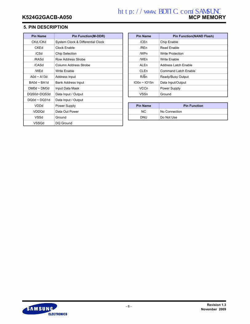
5. PIN DESCRIPTION
Pin Name Pin Function(M-DDR) Pin Name Pin Function(NAND Flash)
CKd,/CKd System Clock & Differential Clock /CEn Chip Enable
CKEd Clock Enable /REn Read Enable
/CSd Chip Selection /WPn Write Protection
/RASd Row Address Strobe /WEn Write Enable
/CASd Column Address Strobe ALEn Address Latch Enable
/WEd Write Enable CLEn Command Latch Enable
A0d ~ A13d Address Input R/Bn Ready/Busy Output
BA0d ~ BA1d Bank Address Input IO0n ~ IO15n Data Input/Output
DM0d ~ DM3d Input Data Mask VCCn Power Supply
DQS0d~DQS3d Data Input / Output VSSn Ground
DQ0d ~ DQ31d Data Input / Output
VDDd Power Supply Pin Name Pin Function
VDDQd Data Out Power NC No Connection
VSSd Ground DNU Do Not Use
VSSQd DQ Ground
Revision 1.3November 2009
- 6 -

K524G2GACB-A050 MCP MEMORYhttp://www.BDTIC.com/SAMSUNG
6. ORDERING INFORMATION
K5 2 4G 2G A C B - A 0 50
Samsung MCP Memory(2chips)
Device TypeNAND Flash + Mobile DDR
NAND Flash Density, Organization4G : 4Gbit, x16
Flash Block ArchitectureC : Uniform Block
VersionB : 3rd Generation
M-DDR Speed50 : 400Mbps@CL3
Operating Voltage A: 1.8V / 1.8V
PackageA : FBGA(HF, LF)
Mobile DDR Density, Organization2G : 2Gbit, x32
NAND Flash Speed0 : None
Revision 1.3November 2009
- 7 -

K524G2GACB-A050 MCP MEMORYhttp://www.BDTIC.com/SAMSUNG
7. FUNCTIONAL BLOCK DIAGRAM
/WPn
CLEn
/WEn
/REn
R/Bn
/CEn
IO0n to IO15n
ALEn
4Gb NANDFlash Memory
VCCn VSSn
DQ0d~DQ31d2Gb Mobile DDR
VDDd VDDQd VSSd VSSQd
CKEd/CSd
/RASd/CASd
CKd,/CKd
/WEdA0d ~ A13d
BA0d ~ BA1dDM0d ~ DM3d
DQS0d ~ DQS3d
Revision 1.3November 2009
- 8 -
K524G2GACB-A050 MCP MEMORYhttp://www.BDTIC.com/SAMSUNG
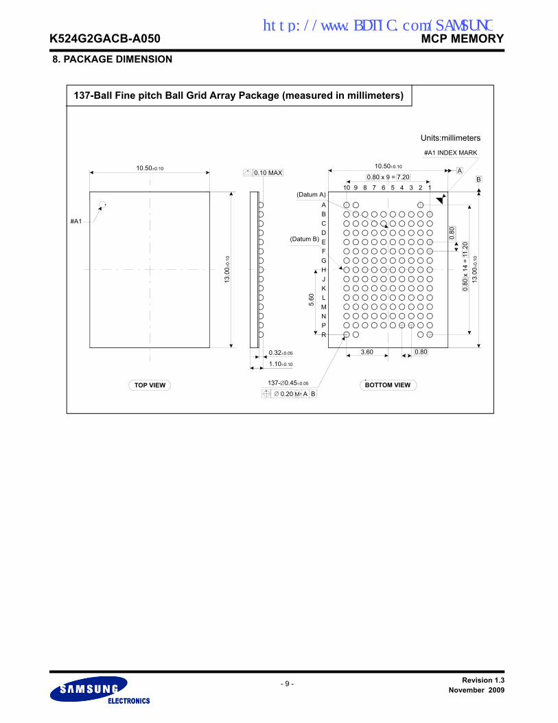
8. PACKAGE DIMENSION
Units:millimeters
0.10 MAX
0.32±0.05
1.10±0.10
TOP VIEW
10.50±0.10
13.0
0±0.
10#A1
137-∅0.45±0.05
0.80
0.20 M A B ∅
(Datum A)14 27 6 5 38
#A1 INDEX MARK
10.50±0.10
13.0
0±0.
10
0.80
9100.80 x 9 = 7.20
0.80
x 1
4 =
11.2
0
ABC
E
G
D
F
HJ
LK
MN
R
(Datum B)
5.60
3.60
BOTTOM VIEW
P
137-Ball Fine pitch Ball Grid Array Package (measured in millimeters)
AB
Revision 1.3November 2009
- 9 -

K524G2GACB-A050 MCP MEMORYhttp://www.BDTIC.com/SAMSUNG
4Gb (256M x16) NAND Flash W-die
Revision 1.3November 2009
- 10 -

K524G2GACB-A050 MCP MEMORYhttp://www.BDTIC.com/SAMSUNG
Figure 1. Functional Block Diagram(x8)
Figure 2. Array Organization(x8)
Table 1. Array address : (x8)
NOTE : Column Address : Starting Address of the Register.* L must be set to "Low".* The device ignores any additional input of address cycles than required.* A30 is Row address for 8G DDP.In case of 4G Mono, A30 must be set to "Low"
I/O 2 I/O 3 I/O 4 I/O 5 I/O 6 I/O 7 Address
1st Cycle A0 A1 A2 A3 A4 A5 A6 A7 Column Address
2nd Cycle A8 A9 A10 A11 *L *L *L *L Column Address
3rd Cycle A12 A13 A14 A15 A16 A17 A18 A19 Row Address
4th Cycle A20 A21 A22 A23 A24 A25 A26 A27 Row Address
5th Cycle A28 A29 *A30 *L *L *L *L *L Row Address
VCC
X-Buffers
Command
I/O Buffers & Latches
Latches& Decoders
Y-BuffersLatches& Decoders
Register
Control Logic& High Voltage
Generator Global Buffers OutputDriver
VSS
A12 - A30*
A0 - A11
Command
CEREWE
CLE WP
I/0 0
I/0 7
VCCVSS
ALE
4,096M + 128M Bit for 4Gb
NAND FlashARRAY
Y-Gating
Data Register & S/A
8,192M + 256M Bit for 8Gb DDP
2K Bytes 64 Bytes
2K Bytes
8 bit
64 Bytes
1 Block = 64 Pages(128K + 4K) Byte
I/O 0 ~ I/O 7
1 Page = (2K + 64)Bytes1 Block = (2K + 64)Byte x 64 Pages = (128K + 4K) Bytes1 Device = (2K+64)B x 64Pages x 4,096 Blocks = 4,224 Mbits for 4Gb
Page Register
4,096 blocks for 4Gb8,192 blocks for 8Gb DDP
1 Device = (2K+64)B x 64Pages x 8,192 Blocks = 8,448 Mbits for 8Gb DDP
I/O 0 I/O 1 I/O 2
Revision 1.3November 2009
- 11 -

K524G2GACB-A050 MCP MEMORYhttp://www.BDTIC.com/SAMSUNG
Figure 3. Functional Block Diagram(x16)
Figure 4. Figure 2-2. Array Organization(x16)
Table 2. Array address : (x16)
NOTE : Column Address : Starting Address of the Register.* L must be set to "Low".* The device ignores any additional input of address cycles than required.* A29 is Row address for 8G DDP.In case of 4G Mono, A29 must be set to "Low"
I/O 2 I/O 3 I/O 4 I/O 5 I/O 6 I/O 7 I/O 8~I/O 15 Address
1st Cycle A0 A1 A2 A3 A4 A5 A6 A7 *L Column Address
2nd Cycle A8 A9 A10 *L *L *L *L *L *L Column Address
3rd Cycle A11 A12 A13 A14 A15 A16 A17 A18 *L Row Address
4th Cycle A19 A20 A21 A22 A23 A24 A25 A26 *L Row Address
5th Cycle A27 A28 *A29 *L *L *L *L *L *L Row Address
VCC
X-Buffers
Command
I/O Buffers & Latches
Latches& Decoders
Y-BuffersLatches& Decoders
Register
Control Logic& High Voltage
Generator Global Buffers OutputDriver
VSS
A11 - A29*
A0 - A10
Command
CEREWE
CLE WP
I/0 0
I/0 15
VCCVSS
ALE
4,096M + 128M Bit for 4Gb
NAND FlashARRAY
Y-Gating
Data Register & S/A
8,192M + 256M Bit for 8Gb DDP
1K Words 32 Words
1K Words
16 bit
32 Words
1 Block = 64 Pages (64K + 2K)Word
I/O 0 ~ I/O 15
1 Page = (1K + 32)Word1 Block = (1K + 32)Word x 64 Pages = (64K + 2K)Words1 Device = (1K + 32)Word x 64Pages x 4,096 Blocks = 4,224 Mbits for 4Gb
Page Register
4,096 blocks for 4Gb8,192 blocks for 8Gb DDP
1 Device = (1K + 32)Word x 64Pages x 8,192 Blocks = 8,448 Mbits for 8Gb DDP
I/O 0 I/O 1 I/O 2
Revision 1.3November 2009
- 12 -

K524G2GACB-A050 MCP MEMORYhttp://www.BDTIC.com/SAMSUNG
1.0 Product IntroductionNAND Flash Memory has addresses multiplexed into 8 I/Os(x16 device case : lower 8 I/Os). This scheme dramatically reduces pin counts andallows system upgrades to future densities by maintaining consistency in system board design. Command, address and data are all writtenthrough I/O's by bringing WE to low while CE is low. Those are latched on the rising edge of WE. Command Latch Enable(CLE) and AddressLatch Enable(ALE) are used to multiplex command and address respectively, via the I/O pins. Some commands require one bus cycle. Forexample, Reset Command, Status Read Command, etc require just one cycle bus. Some other commands, like page read and block eraseand page program, require two cycles: one cycle for setup and the other cycle for execution. Page Read and Page Program need the samefive address cycles following the required command input. In Block Erase operation, however, only the three row address cycles are used.Device operations are selected by writing specific commands into the command register. Table 3 defines the specific commands of theKF94GxxQ2W/KF88GxxQ2W.
In addition to the enhanced architecture and interface, the device incorporates copy-back program feature from one page to another pagewithout need for transporting the data to and from the external buffer memory. Since the time-consuming serial access and data-input cyclesare removed, system performance for solid-state disk application is significantly increased.
Table 3. Command Sets
NOTE : 1) Random Data Input/Output can be executed in a page.
Caution :Any undefined command inputs are prohibited except for above command set of Table 3.
Function 1st Cycle 2nd Cycle Acceptable Command during Busy
Read 00h 30h
Read ID 90h -
Read for Copy Back 00h 35h
Reset FFh - O
Page Program 80h 10h
Copy-Back Program 85h 10h
Block Erase 60h D0h
Random Data Input(1) 85h -
Random Data Output(1) 05h E0h
Read Status 70h - O
Revision 1.3November 2009
- 13 -
K524G2GACB-A050 MCP MEMORYhttp://www.BDTIC.com/SAMSUNG
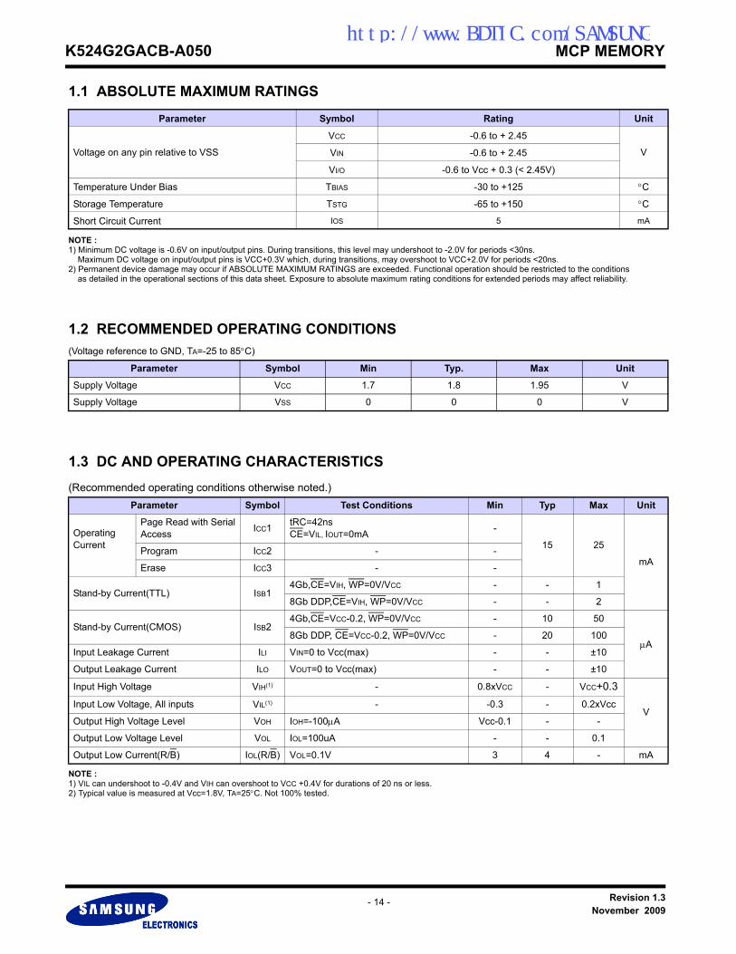
1.1 ABSOLUTE MAXIMUM RATINGS
NOTE : 1) Minimum DC voltage is -0.6V on input/output pins. During transitions, this level may undershoot to -2.0V for periods <30ns. Maximum DC voltage on input/output pins is VCC+0.3V which, during transitions, may overshoot to VCC+2.0V for periods <20ns.2) Permanent device damage may occur if ABSOLUTE MAXIMUM RATINGS are exceeded. Functional operation should be restricted to the conditions as detailed in the operational sections of this data sheet. Exposure to absolute maximum rating conditions for extended periods may affect reliability.
1.2 RECOMMENDED OPERATING CONDITIONS(Voltage reference to GND, TA=-25 to 85°C)
1.3 DC AND OPERATING CHARACTERISTICS(Recommended operating conditions otherwise noted.)
NOTE : 1) VIL can undershoot to -0.4V and VIH can overshoot to VCC +0.4V for durations of 20 ns or less.2) Typical value is measured at Vcc=1.8V, TA=25°C. Not 100% tested.
Parameter Symbol Rating Unit
Voltage on any pin relative to VSS
VCC -0.6 to + 2.45
VVIN -0.6 to + 2.45
VI/O -0.6 to Vcc + 0.3 (< 2.45V)
Temperature Under Bias TBIAS -30 to +125 °C
Storage Temperature TSTG -65 to +150 °C
Short Circuit Current IOS 5 mA
Parameter Symbol Min Typ. Max Unit
Supply Voltage VCC 1.7 1.8 1.95 V
Supply Voltage VSS 0 0 0 V
Parameter Symbol Test Conditions Min Typ Max Unit
Operating Current
Page Read with SerialAccess ICC1 tRC=42ns
CE=VIL, IOUT=0mA -
15 25
mAProgram ICC2 - -
Erase ICC3 - -
Stand-by Current(TTL) ISB14Gb,CE=VIH, WP=0V/VCC - - 1
8Gb DDP,CE=VIH, WP=0V/VCC - - 2
Stand-by Current(CMOS) ISB24Gb,CE=VCC-0.2, WP=0V/VCC - 10 50
µA8Gb DDP, CE=VCC-0.2, WP=0V/VCC - 20 100
Input Leakage Current ILI VIN=0 to Vcc(max) - - ±10
Output Leakage Current ILO VOUT=0 to Vcc(max) - - ±10
Input High Voltage VIH(1) - 0.8xVCC - VCC+0.3
VInput Low Voltage, All inputs VIL(1) - -0.3 - 0.2xVcc
Output High Voltage Level VOH IOH=-100µA Vcc-0.1 - -
Output Low Voltage Level VOL IOL=100uA - - 0.1
Output Low Current(R/B) IOL(R/B) VOL=0.1V 3 4 - mA
Revision 1.3November 2009
- 14 -

K524G2GACB-A050 MCP MEMORYhttp://www.BDTIC.com/SAMSUNG
1.4 VALID BLOCK
NOTE : 1) The device may include initial invalid blocks when first shipped. Additional invalid blocks may develop while being used. The number of valid blocks is presented
with both cases of invalid blocks considered. Invalid blocks are defined as blocks that contain one or more bad bits. Do not erase or program factory-marked badblocks. Refer to the attached technical notes for appropriate management of invalid blocks.
2) The 1st block, which is placed on 00h block address, is guaranteed to be a valid block up to 1K program/erase cycles with x8 : 1bit/ 512Byte, x16 : 1bit/256Word ECC.
3) Each mono chip in th KF88GxxQ2W has maximum 40 invalid blocks.
1.5 AC TEST CONDITION(TA=-25 to 85°C, Vcc=1.7V~1.95V unless otherwise noted)
1.6 CAPACITANCE(TA=25°C, VCC=1.8V, f=1.0MHz)
NOTE :Capacitance is periodically sampled and not 100% tested.
1.7 MODE SELECTION
NOTE : 1) X can be VIL or VIH.2) WP should be biased to CMOS high or CMOS low for standby.
Parameter Symbol Min Typ. Max Unit
4Gb NVB 4,016 - 4,096 Blocks
8Gb DDP NVB 8.032 - 8,192 Blocks
Parameter Value
Input Pulse Levels 0V to Vcc
Input Rise and Fall Times 5ns
Input and Output Timing Levels Vcc/2
Output Load 1 TTL GATE and CL=30pF
Item Symbol Test Condition Min Max Unit
Input/Output Capacitance (Mono) CI/O VIL=0V - 10 pF
Input Capacitance (Mono) CIN VIN=0V - 10 pF
Input/Output Capacitance (DDP) CI/O VIL=0V - 20 pF
Input Capacitance (DDP) CIN VIN=0V - 20 pF
CLE ALE CE WE RE WP Mode
H L L H XRead Mode
Command Input
L H L H X Address Input(5clock)
H L L H HWrite Mode
Command Input
L H L H H Address Input(5clock)
L L L H H Data Input
L L L H X Data Output
X X X X H X During Read(Busy)
X X X X X H During Program(Busy)
X X X X X H During Erase(Busy)
X X(1) X X X L Write Protect
X X H X X 0V/VCC(2) Stand-by
Revision 1.3November 2009
- 15 -

K524G2GACB-A050 MCP MEMORYhttp://www.BDTIC.com/SAMSUNG
1.8 Read / Program / Erase Characteristics
NOTE :1) Typical program time is defined as the time within which more than 50% of the whole pages are programmed at 1.8V Vcc and 25°C temperature.
1.9 AC Timing Characteristics for Command / Address / Data Input
NOTE : 1) The transition of the corresponding control pins must occur only once while WE is held low2) tADL is the time from the WE rising edge of final address cycle to the WE rising edge of first data cycle
Parameter Symbol Min Typ Max Unit
Program Time tPROG - 250 750 µs
Number of Partial Program Cycles Nop - - 4 cycles
Block Erase Time tBERS - 2 10 ms
Parameter Symbol Min Max Unit
CLE Setup Time tCLS(1) 21 - ns
CLE Hold Time tCLH 5 - ns
CE Setup Time tCS(1) 21 - ns
CE Hold Time tCH 5 - ns
WE Pulse Width tWP 21 - ns
ALE Setup Time tALS(1) 21 - ns
ALE Hold Time tALH 5 - ns
Data Setup Time tDS(1) 20 - ns
Data Hold Time tDH 5 - ns
Write Cycle Time tWC 40 - ns
WE High Hold Time tWH 10 - ns
Address to Data Loading Time tADL(2) 100 - ns
Revision 1.3November 2009
- 16 -

K524G2GACB-A050 MCP MEMORYhttp://www.BDTIC.com/SAMSUNG
1.10 AC Characteristics for Operation
NOTE : 1) If reset command(FFh) is written at Ready state, the device goes into Busy for maximum 5µs.
Parameter Symbol Min Max Unit
Data Transfer from Cell to Register tR - 40 µs
ALE to RE Delay tAR 10 - ns
CLE to RE Delay tCLR 10 - ns
Ready to RE Low tRR 20 - ns
RE Pulse Width tRP 21 - ns
WE High to Busy tWB - 100 ns
WP Low to WE Low (disable mode)tWW 100 - ns
WP High to WE Low (enable mode)
Read Cycle Time tRC 42 - ns
RE Access Time tREA - 30 ns
CE Access Time tCEA - 35 ns
RE High to Output Hi-Z tRHZ - 100 ns
CE High to Output Hi-Z tCHZ - 30 ns
CE High to ALE or CLE Don’t Care tCSD 0 - ns
RE High to Output Hold tROH 15 - ns
CE High to Output Hold tCOH 15 - ns
RE High Hold Time tREH 10 - ns
Output Hi-Z to RE Low tIR 0 - ns
RE High to WE Low tRHW 100 - ns
WE High to RE Low tWHR 60 - ns
Device Resetting Time(Read/Program/Erase) tRST - 5/10/500(1) µs
Revision 1.3November 2009
- 17 -

K524G2GACB-A050 MCP MEMORYhttp://www.BDTIC.com/SAMSUNG
2.0 NAND Flash Technical Notes
2.1 Initial Invalid Block(s)Initial invalid blocks are defined as blocks that contain one or more initial invalid bits whose reliability is not guaranteed by Samsung. The infor-mation regarding the initial invalid block(s) is called the initial invalid block information. Devices with initial invalid block(s) have the same qual-ity level as devices with all valid blocks and have the same AC and DC characteristics. An initial invalid block(s) does not affect theperformance of valid block(s) because it is isolated from the bit line and the common source line by a select transistor. The system designmust be able to mask out the initial invalid block(s) via address mapping. The 1st block, which is placed on 00h block address, is guaranteedto be a valid block up to 1K program/erase cycles with x8:1bit/ 512Byte, x16:1bit/256Word ECC.
2.2 Identifying Initial Invalid Block(s)All device locations are erased(FFh) except locations where the initial invalid block(s) information is written prior to shipping. The initial invalidblock(s) status is defined by the 1st byte(1st word) in the spare area. Samsung makes sure that either the 1st or 2nd page of every initialinvalid block has non-FFh data at the column address of 2048(x16:1024). Since the initial invalid block information is also erasable in mostcases, it is impossible to recover the information once it has been erased. Therefore, the system must be able to recognize the initial invalidblock(s) based on the original initial invalid block information and create the initial invalid block table via the following suggested flow chart(Fig-ure 5). Any intentional erasure of the original initial invalid block information is prohibited.
Figure 5. Flow chart to create initial invalid block table
* Check "FFh(x16:FFFFh)" at the
Start
Set Block Address = 0
Check
Increment Block Address
Last Block ?
End
No
Yes
Yes
Create (or update) NoInitial
of the 1st and 2nd page in the block
Invalid Block(s) Table"FFh(x16:FFFFh)"
column address 2048(x16:1024)
Revision 1.3November 2009
- 18 -

K524G2GACB-A050 MCP MEMORYhttp://www.BDTIC.com/SAMSUNG
NAND Flash Technical Notes (Continued)
2.3 Error in write or read operationWithin its life time, additional invalid blocks may develop with NAND Flash memory. Refer to the qualification report for the actual data. Blockreplacement should be done upon erase or program error.
ECC : Error Correcting Code --> Hamming code Example) 1bit correction & 512-byte
Note) A repetitive page read operation on the same block without erase may cause bit errors, which could be accumulated over time and exceed the coverage of ECC. Software scheme such as caching into RAM is recommended.
Program Flow Chart
Failure Mode Detection and Countermeasure sequence
Write Erase Failure Status Read after Erase --> Block Replacement
Program Failure Status Read after Program --> Block Replacement
Read Up to 1 Bit-Failure Verity ECC -> ECC Correction
Start
I/O 6 = 1 ?
I/O 0 = 0 ? No*
Write 80h
Write Address
Write Data
Write 10h
Read Status Register
Program Completed
or R/B = 1 ?
Program Error
Yes
No
Yes
: If program operation results in an error, map out the block including the page in error and copy the target data to another block.
*
Revision 1.3November 2009
- 19 -

K524G2GACB-A050 MCP MEMORYhttp://www.BDTIC.com/SAMSUNG
NAND Flash Technical Notes (Continued)
Block Replacement
* Step1When an error happens in the nth page of the Block ’A’ during erase or program operation. * Step2Copy the data in the 1st ~ (n-1)th page to the same location of another free block. (Block ’B’)* Step3Then, copy the nth page data of the Block ’A’ in the buffer memory to the nth page of the Block ’B’.* Step4Do not erase or program to Block ’A’ by creating an ’invalid block’ table or other appropriate scheme.
Erase Flow Chart Read Flow Chart
Start
I/O 6 = 1 ?
I/O 0 = 0 ? No*
Write 60h
Write Block Address
Write D0h
Read Status Register
or R/B = 1 ?
Erase Error
Yes
No
: If erase operation results in an error, map outthe failing block and replace it with another block. *
Erase Completed
Yes
Start
Verify ECC No
Write 00h
Write Address
Read Data
ECC Generation
Reclaim the Error
Page Read Completed
Yes
Write 30h
Buffer memory of the controller.
1stBlock A
Block B
(n-1)thnth
(page)
∼
1st
(n-1)thnth
(page)
∼
an error occurs.1
2
Revision 1.3November 2009
- 20 -

K524G2GACB-A050 MCP MEMORYhttp://www.BDTIC.com/SAMSUNG
NAND Flash Technical Notes (Continued)
2.4 Addressing for program operationWithin a block, the pages must be programmed consecutively from the LSB(least significant bit) page of the block to the MSB(most significant bit) pages of the block. Random page address programming is prohibited. In this case, the definition of LSB page is the LSB among the pages to be programmed. Therefore, LSB doesn't need to be page 0.
From the LSB page to MSB page
DATA IN: Data (1) Data (64)
(1)(2)(3)
(32)
(64)
Data register
Page 0Page 1Page 2
Page 31
Page 63
Ex.) Random page program (Prohibition)
DATA IN: Data (1) Data (64)
(2)(32)(3)
(1)
(64)
Data register
Page 0Page 1Page 2
Page 31
Page 63
:
:
:
:
Revision 1.3November 2009
- 21 -

K524G2GACB-A050 MCP MEMORYhttp://www.BDTIC.com/SAMSUNG
2.5 System Interface Using CE don’t-care.For an easier system interface, CE may be inactive during the data-loading or serial access as shown below. The internal2,112byte(1,056Word) data registers are utilized as separate buffers for this operation and the system design gets more flexible. In addition,for voice or audio applications which use slow cycle time on the order of µ-seconds, de-activating CE during the data-loading and serialaccess would provide significant savings in power consumption.
Figure 6. Program Operation with CE don’t-care.
Figure 7. Read Operation with CE don’t-care.
CE
WEtWP
tCHtCS
Address(5Cycles)80h Data Input
CE
CLE
ALE
WE
Data Input
CE don’t-care
10h
tCEA
out
tREA
CE
RE
I/Ox
I/Ox
≈≈
≈≈
≈≈
≈≈
≈≈
≈ ≈
Address(5Cycle)00h
CE
CLE
ALE
WE
Data Output(serial access)
CE don’t-care
R/B tR
RE
30hI/Ox
≈
≈≈
≈≈
≈
≈≈
≈≈
≈
≈
Revision 1.3November 2009
- 22 -

K524G2GACB-A050 MCP MEMORYhttp://www.BDTIC.com/SAMSUNG
NOTE :
DeviceI/O DATA ADDRESS
I/Ox Data In/Out Col. Add1 Col. Add2 Row Add1 Row Add2 Row Add3
4Gb(x8) I/O 0 ~ I/O 7 ~2,112byte A0~A7 A8~A11 A12~A19 A20~A27 A28~A29
8Gb DDP(x8) I/O 0 ~ I/O 7 ~2,112byte A0~A7 A8~A11 A12~A19 A20~A27 A28~A30
4Gb(x16) I/O 0 ~ I/O 15 ~1,056Word A0~A7 A8~A10 A11~A18 A19~A26 A27~A28
8Gb DDP(x16) I/O 0 ~ I/O 15 ~1,056Word A0~A7 A8~A10 A11~A18 A19~A26 A27~A29
Revision 1.3November 2009
- 23 -

K524G2GACB-A050 MCP MEMORYhttp://www.BDTIC.com/SAMSUNG
3.0 TIMING DIAGRAMS
3.1 Command Latch Cycle
CE
WE
CLE
ALE
Command
tCLS
tCS
tCLH
tCH
tWP
tALS tALH
tDS tDH
I/Ox
Revision 1.3November 2009
- 24 -

K524G2GACB-A050 MCP MEMORYhttp://www.BDTIC.com/SAMSUNG
3.2 Address Latch Cycle
3.3 Input Data Latch Cycle
CE
WE
CLE
ALE
Col. Add1
tCStWC
tWP
tALS
tDStDH
tALH tALStWH
tWC
tWP
tDStDH
tALH tALStWH
tWC
tWP
tDH
tALH tALStWH
tDStDH
tWP
I/Ox Col. Add2 Row Add1 Row Add2
tWC
tWHtALH tALS
tDStDH
Row Add3
tALH
tCLS
tDS
CE
CLE
WE
DIN 0 DIN 1 DIN final
ALE
tALS
tCLH
tWC
tCH
tDS tDH tDStDH
tDStDH
tWP
tWH
tWP tWP≈≈
≈
I/Ox
≈≈
≈
Revision 1.3November 2009
- 25 -

K524G2GACB-A050 MCP MEMORYhttp://www.BDTIC.com/SAMSUNG
3.4 * Serial Access Cycle after Read(CLE=L, WE=H, ALE=L)
NOTE :Transition is measured at ±200mV from steady state voltage with load.This parameter is sampled and not 100% tested.
3.5 Status Read Cycle
RE
CE
R/B
Dout Dout Dout
tRC
tREA
tRR
tROH
tREAtREH
tREA tCOH
tRHZ
≈≈
≈≈
I/Ox
tCHZ
tRHZ
tRP
CE
WE
CLE
RE
70h Status Output
tCLR
tCLH
tWPtCH
tDStDH tREAtIR
tRHOH
tCOHtWHR
tCEA
tCLS
I/Ox
tCHZ
tRHZ
tCS
Revision 1.3November 2009
- 26 -

K524G2GACB-A050 MCP MEMORYhttp://www.BDTIC.com/SAMSUNG
3.6 Read Operation
3.7 Read Operation(Intercepted by CE)
CE
CLE
R/B
WE
ALE
RE
Busy
00h Col. Add1 Col. Add2 Row Add1 Dout N Dout N+1
Column Address Row Address
tWBtAR
tR tRCtRHZ
tRR
Dout M
tWC
≈≈
≈
Row Add2 30h
tCLR
I/Ox Row Add3
CE
CLE
R/B
WE
ALE
RE
Busy
00h Dout N Dout N+1 Dout N+2
Row AddressColumn Address
tWB
tAR
tCHZ
tR
tRR
tRC
30hI/Ox Col. Add1 Col. Add2 Row Add1 Row Add2 Row Add3
tCOH
tCLR
tCSD
Revision 1.3November 2009
- 27 -

K524G2GACB-A050 MCP MEMORYhttp://www.BDTIC.com/SAMSUNG
3.8 Random Data Output In a Page
CE
CLE
R/B
WE
ALE
RE
Busy
00h
Dout
NDo
ut N
+1
Row
Addr
ess
Colu
mn
Addr
ess
tWB
tAR
tR tRR
30h
05h
Colu
mn
Addr
ess
Dout
MDo
ut M
+1I/O
xC
ol. A
dd1
Col
. Add
2R
ow A
dd1
Row
Add2
Col A
dd1
Col A
dd2
Row
Add3
tCLR E0
h
tWH
R
tRE
AtR
C
tRH
W
Revision 1.3November 2009
- 28 -

K524G2GACB-A050 MCP MEMORYhttp://www.BDTIC.com/SAMSUNG
3.9 Page Program Operation
NOTE : tADL is the time from the WE rising edge of final address cycle to the WE rising edge of first data cycle.
CE
CLE
R/B
WE
ALE
RE
80h 70h I/O0DinN
Din 10hMSerialData
Input Command Column Address Row Address 1 up to m ByteSerial Input
ProgramCommand
Read StatusCommand
I/O0=0 Successful ProgramI/O0=1 Error in Program
tPROGtWB
tWC tWC tWC
≈≈
≈
≈
I/Ox Co.l Add1 Col. Add2 Row Add1 Row Add2 Row Add3
tADLtWHR
Revision 1.3November 2009
- 29 -
K524G2GACB-A050 MCP MEMORYhttp://www.BDTIC.com/SAMSUNG
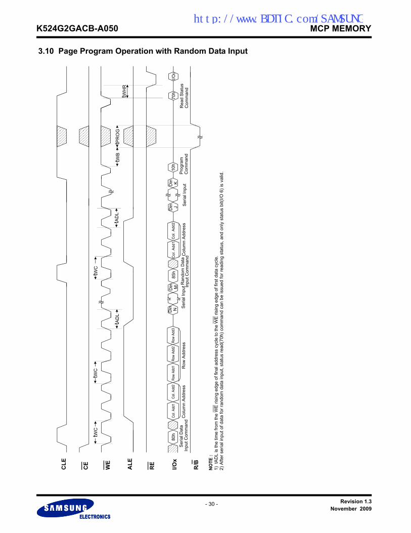
3.10 Page Program Operation with Random Data Input
CE
CLE
R/B
WE
ALE
RE
80h
70h
I/O0
Din N
Din
10h
MS
eria
l Dat
aIn
put C
omm
and
Col
umn
Add
ress
Row
Add
ress
Ser
ial I
nput
Prog
ram
Com
man
dR
ead
Stat
usC
omm
and
tPR
OG
tWB
tWC
tWC
≈ ≈
≈
≈
85h
Ran
dom
Dat
aIn
put C
omm
andC
olum
n A
ddre
ss
tWC
Din J
Din K
Seria
l Inp
ut
≈ ≈
I/Ox
Col.
Add1
Col. A
dd2
Row
Add1
Row
Add2
Col
. Add
1C
ol. A
dd2
Row
Add3
≈
tAD
LtA
DL
tWH
R
NO
TE :
1) t
ADL
is th
e tim
e fro
m th
e W
E ris
ing
edge
of f
inal
add
ress
cyc
le to
the
WE
risin
g ed
ge o
f firs
t dat
a cy
cle.
2) A
fter s
eria
l inp
ut o
f dat
a fo
r ran
dom
dat
a in
put,
stat
us re
ad(7
0h) c
omm
and
can
be is
sued
for r
eadi
ng s
tatu
s, a
nd o
nly
stat
us b
it(I/O
6) i
s va
lid.
Revision 1.3November 2009
- 30 -

K524G2GACB-A050 MCP MEMORYhttp://www.BDTIC.com/SAMSUNG
3.11 Copy-Back Program Operation with Random Data Input
00h
I/Ox
85h
Colum
n Ad
dres
sRo
w Ad
dres
s R
ead
Stat
us C
omm
and
I/O0=
0 Su
cces
sful P
rogr
amI/O
0=1
Erro
r in
Prog
ram
tPR
OG
tWB
tWC
≈
Busy
tWB tR
Busy
≈
10h
Copy
-Bac
k Da
taIn
put C
omm
and
35h
Colum
n Add
ress
Row
Addr
ess
Data
1Da
ta N
≈≈
Col A
dd1
Col A
dd2
Row A
dd1
Row A
dd2Co
l Add
1Co
l Add
2Ro
w Ad
d1Ro
w Add
2Row
Add3
Row A
dd370
h
tAD
L
tWH
R
Data
1Da
ta N
≈≈
tRC
CE
CLE
R/B
WE
ALE
RE
I/Ox
NO
TE :
1) t
ADL
is th
e tim
e fro
m th
e W
E ris
ing
edge
of f
inal
add
ress
cyc
le to
the
WE
risin
g ed
ge o
f firs
t dat
a cy
cle.
Revision 1.3November 2009
- 31 -

K524G2GACB-A050 MCP MEMORYhttp://www.BDTIC.com/SAMSUNG
3.12 Block Erase Operation
CE
CLE
R/B
WE
ALE
RE
60h
Erase CommandRead StatusCommand
I/O0=1 Error in Erase
D0h 70h I/O 0
Busy
tWB tBERS
I/O0=0 Successful Erase
Row Address
tWC
≈Auto Block EraseSetup Command
I/Ox Row Add1 Row Add2 Row Add3
tWHR
Revision 1.3November 2009
- 32 -

K524G2GACB-A050 MCP MEMORYhttp://www.BDTIC.com/SAMSUNG
3.13 Read ID Operation
3.13.1 ID Definition Table
90 ID : Access command = 90H
Device Device Code (2nd Cycle) 3rd Cycle 4th Cycle 5th Cycle
4Gb(x8) ACh 00h 15h 56h
8Gb DDP(x8) A3h 01h 15h 5Ah
4Gb(x16) BCh 00h 55h 56h
8Gb DDP(x16) B3h 01h 55h 5Ah
Description
1st Byte2nd Byte3rd Byte4th Byte5th Byte
Maker CodeDevice CodeInternal Chip NumberPage Size, Block Size,Redundant Area Size, OrganizationPlane Number, Plane Size, ECC Level
CE
CLE
WE
ALE
RE
90h
Read ID Command Maker Code Device Code
00h ECh
tREA
Address 1cycle
I/Ox
tAR
Device 4th cyc.Code 3rd cyc. 5th cyc.
Revision 1.3November 2009
- 33 -

K524G2GACB-A050 MCP MEMORYhttp://www.BDTIC.com/SAMSUNG
3rd ID Data
4th ID Data
ITEM DescriptionI/O #
7 6 5 4 3 2 1 0
Internal Chip Number
1 2 4 8
0011
0101
Cell Type
2 Level Cell 4 Level Cell 8 Level Cell 16 Level Cell
0011
0101
Number of Simultaneously Programmed Pages
1 2 4 8
0011
0101
Interleave ProgramBetween Multii-Chips
Not supportedsupported
0 1
Cache Program Not supportedsupported
0 1
ITEM DescriptionI/O #
7 6 5 4 3 2 1 0
Page Size (without Redundant Area)
1KB 2KB 4KB 8KB
0011
0101
Block Size (without Redundant Area)
64KB 128KB 256KB 512KB
0011
0101
Redundant Area Size (Byte/512byte)
816
ReservedReserved
0011
0101
Organization X8X16
01
Reserved 0 or 1
Revision 1.3November 2009
- 34 -

K524G2GACB-A050 MCP MEMORYhttp://www.BDTIC.com/SAMSUNG
5th ID Data
ITEM DescriptionI/O #
7 6 5 4 3 2 1 0
ECC level
1bit ECC/512Byte2bit ECC/512Byte4bit ECC/512Byte
Reserved
0011
0101
Plane Number
1248
0011
0101
Plane Size (without Redundant Area)
64KB 128KB 256KB 512KB
1Gb2Gb4Gb8Gb
00001111
00110011
01010101
Reseved Reserved 0
Revision 1.3November 2009
- 35 -

K524G2GACB-A050 MCP MEMORYhttp://www.BDTIC.com/SAMSUNG
4.0 Device Operation
4.1 PAGE READPage read is initiated by writing 00h-30h to the command register along with five address cycles. After initial power up, 00h command islatched. Therefore only five address cycles and 30h command initiates that operation after initial power up. The 2,112 bytes(1,056 Wrods) ofdata within the selected page are transferred to the data registers in 40µs(tR) typically. The system controller can detect the completion of thisdata transfer(tR) by analyzing the output of R/B pin. Once the data in a page is loaded into the data registers, they may be read out in 42nscycle time by sequentially pulsing RE. The repetitive high to low transitions of the RE clock make the device output the data starting from theselected column address up to the last column address. The device may output random data in a page instead of the consecutive sequential data by writing random data output command. The col-umn address of next data, which is going to be out, may be changed to the address which follows random data output command. Randomdata output can be operated multiple times regardless of how many times it is done in a page.
Figure 8. Read Operation
Address(5Cycle)00h
Col. Add.1,2 & Row Add.1,2,3
Data Output(Serial Access)
Data Field Spare Field
CE
CLE
ALE
R/B
WE
RE
tR
30hI/Ox
≈≈
≈≈
≈≈
Revision 1.3November 2009
- 36 -

K524G2GACB-A050 MCP MEMORYhttp://www.BDTIC.com/SAMSUNG
4.2 PAGE PROGRAMThe device is programmed basically on a page basis, but it does allow multiple partial page programming of a byte(a word) or consecutivebyte up to 2,112 bytes(1,056 Wrods), in a single page program cycle. The number of consecutive partial page programming operation withinthe same page without an intervening erase operation must not exceed 4 times for a single page. The addressing should be done in sequen-tial order in a block. A page program cycle consists of a serial data loading period in which up to 2,112 bytes(1,056 Wrods) of data may beloaded into the data register, followed by a non-volatile programming period where the loaded data is programmed into the appropriate cell. The serial data loading period begins by inputting the Serial Data Input command(80h), followed by the five cycle address inputs and thenserial data loading. The bytes(words) other than those to be programmed do not need to be loaded. The device supports random data input ina page. The column address for the next data, which will be entered, may be changed to the address which follows random data input com-mand(85h). Random data input may be operated multiple times regardless of how many times it is done in a page.The Page Program confirm command(10h) initiates the programming process. Writing 10h alone without previously entering the serial data will not initiate the programming process. The internal write state controller automatically executes the algorithms and timings necessary for program and verify, thereby freeing the system controller for other tasks. Once the program process starts, the Read Status Register com-mand may be entered to read the status register. The system controller can detect the completion of a program cycle by monitoring the R/B output, or the Status bit(I/O 6) of the Status Register. Only the Read Status command and Reset command are valid while programming is in progress. When the Page Program is complete, the Write Status Bit(I/O 0) may be checked(Figure 9). The internal write verify detects only errors for "1"s that are not successfully programmed to "0"s. The command register remains in Read Status command mode until another valid command is written to the command register.
Figure 9. Program & Read Status Operation
Figure 10. Random Data Input In a Page
80h
R/B
Address & Data Input I/O0 Pass
Data
10h 70h
Fail
tPROG
I/OxCol. Add.1,2 & Row Add.1,2,3
"0"
"1"
80h
R/B
Address & Data Input I/O0 Pass10h 70h
Fail
tPROG
85h Address & Data InputI/OxCol. Add.1,2 & Row Add1,2,3 Col. Add.1,2
Data Data
"0"
"1"
Revision 1.3November 2009
- 37 -

K524G2GACB-A050 MCP MEMORYhttp://www.BDTIC.com/SAMSUNG
4.3 COPY-BACK PROGRAM
Copy-Back program with Read for Copy-Back is configured to quickly and efficiently rewrite data stored in one page without data re-loadingwhen the bit error is not in data stored. Since the time-consuming re-loading cycles are removed, the system performance is improved. Thebenefit is especially obvious when a portion of a block is updated and the rest of the block also needs to be copied to the newly assigned freeblock. Copy-Back operation is a sequential execution of Read for Copy-Back and of copy-back program with the destination page address. Aread operation with "35h" command and the address of the source page moves the whole 2,112 bytes(1,056 Wrods) data into the internal databuffer. A bit error is checked by sequential reading the data output. In the case where there is no bit error, the data do not need to be reloaded.Therefore Copy-Back program operation is initiated by issuing Page-Copy Data-Input command (85h) with destination page address. Actualprogramming operation begins after Program Confirm command (10h) is issued. Once the program process starts, the Read Status Registercommand (70h) may be entered to read the status register. The system controller can detect the completion of a program cycle by monitoringthe R/B output, or the Status bit(I/O 6) of the Status Register. When the Copy-Back Program is complete, the Write Status Bit(I/O 0) may bechecked(Figure 11 & Figure 12). The command register remains in Read Status command mode until another valid command is written to thecommand register.During copy-back program, data modification is possible using random data input command (85h) as shown in Figure 12.
Figure 11. Page Copy-Back Program Operation
NOTE :1) Copy-Back Program operation is allowed only within the same memory plane.
Figure 12. Page Copy-Back Program Operation with Random Data Input
4.4 BLOCK ERASEThe Erase operation is done on a block basis. Block address loading is accomplished in three cycles initiated by an Erase Setup com-mand(60h). Only Block address is valid while page address is ignored. The Erase Confirm command(D0h) following the block address loadinginitiates the internal erasing process. This two-step sequence of setup followed by execution command ensures that memory contents are notaccidentally erased due to external noise conditions.At the rising edge of WE after the erase confirm command input, the internal write controller handles erase and erase-verify. When the eraseoperation is completed, the Write Status Bit(I/O 0) may be checked. Figure 13 details the sequence.
"0"
"1"
00h
R/B
Add.(5Cycles) I/O0 Pass
Fail
tPROGtR
Source Address Destination Address
I/OxCol. Add.1,2 & Row Add.1,2,3Col. Add.1,2 & Row Add.1,2,3
35h Data Output 85h Add.(5Cycles) 10h 70h
≈≈
R/B
Source Address Destination Address There is no limitation for the number of repetition.
I/OxCol. Add.1,2 & Row Add.1,2,3 Col. Add.1,2 & Row Add.1,2,3 Col. Add.1,2
00h Add.(5Cycles) 35h
tR
Data Output 85h Add.(5Cycles) Data
≈≈
85h Add.(2Cycles) Data 10h
tPROG
70h
Revision 1.3November 2009
- 38 -

K524G2GACB-A050 MCP MEMORYhttp://www.BDTIC.com/SAMSUNG
Figure 13. Block Erase Operation
4.5 READ STATUSThe device contains a Status Register which may be read to find out whether program or erase operation is completed, and whether the pro-gram or erase operation is completed successfully. After writing 70h command to the command register, a read cycle outputs the content ofthe Status Register to the I/O pins on the falling edge of CE or RE, whichever occurs last. This two line control allows the system to poll theprogress of each device in multiple memory connections even when R/B pins are common-wired. RE or CE does not need to be toggled forupdated status. Refer to Table 4 for specific Status Register definitions. The command register remains in Status Read mode until further com-mands are issued to it. Therefore, if the status register is read during a random read cycle, the read command(00h) should be given beforestarting read cycles.
Table 4. Status Register Definition for 70h Command
NOTE : 1) I/Os defined ’Not use’ are recommended to be masked out when Read Status is being executed.
I/O Page Program Block Erase Read Definition
I/O 0 Pass/Fail Pass/Fail Not Use Pass : "0" Fail : "1"
I/O 1 Not use Not use Not use Don’t -cared
I/O 2 Not use Not use Not use Don’t -cared
I/O 3 Not Use Not Use Not use Don’t -cared
I/O 4 Not Use Not Use Not Use Don’t -cared
I/O 5 Not Use Not Use Not Use Don’t -cared
I/O 6 Ready/Busy Ready/Busy Ready/Busy Busy : "0" Ready : "1"
I/O 7 Write Protect Write Protect Write Protect Protected : "0" Not Protected : "1"
60h
Row Add 1,2,3
R/B
Address Input(3Cycle) I/O0 PassD0h 70h
Fail
tBERS
I/Ox"0"
"1"
Revision 1.3November 2009
- 39 -
K524G2GACB-A050 MCP MEMORYhttp://www.BDTIC.com/SAMSUNG
4.6 Read IDThe device contains a product identification mode, initiated by writing 90h to the command register, followed by an address input of 00h. Fiveread cycles sequentially output the manufacturer code(ECh), and the device code and 3rd, 4th, 5th cycle ID respectively. The command reg-ister remains in Read ID mode until further commands are issued to it. Figure 14 shows the operation sequence.
Figure 14. Read ID Operation
4.7 RESETThe device offers a reset feature, executed by writing FFh to the command register. When the device is in Busy state during random read, pro-gram or erase mode, the reset operation will abort these operations. The contents of memory cells being altered are no longer valid, as thedata will be partially programmed or erased. The command register is cleared to wait for the next command, and the Status Register is clearedto value C0h when WP is high. If the device is already in reset state a new reset command will be accepted by the command register. The R/B pin changes to low for tRST after the Reset command is written. Refer to Figure 15 below.
Figure 15. RESET Operation
Table 5. Device Status
Device Device Code (2nd Cycle) 3rd Cycle 4th Cycle 5th Cycle
4Gb(x8) ACh 00h 15h 54h
8Gb DDP(x8) A3h 01h 15h 58h
4Gb(x16) BCh 00h 55h 54h
8Gb DDP(x16) B3h 01h 55h 58h
After Power-up After Reset
Operation mode Mode 00h Command is latched Waiting for next command
CE
CLE
I/OX
ALE
RE
WE
90h 00h
Address. 1cycle Maker code Device code
tCEA
tAR
tREA
tWHR
tCLR
Device 4th Cyc.CodeECh 3rd Cyc. 5th Cyc.
FFhI/OX
R/BtRST
Revision 1.3November 2009
- 40 -

K524G2GACB-A050 MCP MEMORYhttp://www.BDTIC.com/SAMSUNG
4.8 READY/BUSYThe device has a R/B output that provides a hardware method of indicating the completion of a page program, erase and random read com-pletion. The R/B pin is normally high but transitions to low after program or erase command is written to the command register or random readis started after address loading. It returns to high when the internal controller has finished the operation. The pin is an open-drain driverthereby allowing two or more R/B outputs to be Or-tied. Because pull-up resistor value is related to tr(R/B) and current drain duringbusy(ibusy) , an appropriate value can be obtained with the following reference chart(Fig.17). Its value can be determined by the followingguidance.
Figure 16. Rp vs tr ,tf & Rp vs ibusy
Rp value guidance
where IL is the sum of the input currents of all devices tied to the R/B pin.Rp(max) is determined by maximum permissible limit of tr
VCC
R/Bopen drain output
Device
GND
Rp ibusy
Busy
Ready Vcc
VOH
tf tr
VOL
1.8V device - VOL : 0.1V, VOH : VCC-0.1V
CL
Vcctr,
tf [s
]
Ibus
y [A
]
Rp(ohm)
Ibusy
tr
@ Vcc = 1.8V, Ta = 25°C , CL = 30pF
1K 2K 3K 4K
100n
200n 2m
1m
30tf
60
90
120
1.7 1.7 1.7 1.7
1.70
0.85
0.570.43
Rp(min, 1.8V part) =VCC(Max.) - VOL(Max.)
IOL + ΣIL =
1.85V
3mA + ΣIL
Revision 1.3November 2009
- 41 -

K524G2GACB-A050 MCP MEMORYhttp://www.BDTIC.com/SAMSUNG
5.0 DATA PROTECTION & POWER UP SEQUENCEThe device is designed to offer protection from any involuntary program/erase during power-transitions. An internal voltage detector disablesall functions whenever Vcc is below about 1.1V. WP pin provides hardware protection and is recommended to be kept at VIL during power-upand power-down. A recovery time of minimum 1ms is required before internal circuit gets ready for any command sequences as shown in Fig-ure 17. The two step command sequence for program/erase provides additional software protection.
Figure 17. AC Waveforms for Power Transition
VCC
WP
High
WE
Ready/Busy
5 ms max Operation
1ms
~ 1.5V ~ 1.5V
Invalid Don’t care
Don’t care≈
≈≈
≈≈
Revision 1.3November 2009
- 42 -

K524G2GACB-A050 MCP MEMORYhttp://www.BDTIC.com/SAMSUNG
5.1 WP AC TIMING GUIDE
Enabling WP during erase and program busy is prohibited.The erase and program operations are enabled and disabled as follows:
Figure 18. Program Operation
Figure 19. Erase Operation
1. Enable Mode
≈
80h 10h
WE
I/O
WP
R/B tww(min.100ns)
2. Disable Mode
≈80h 10h
WE
I/O
WP
R/B tww(min.100ns)
1. Enable Mode
60h D0h
WE
I/O
WP
R/B tww(min.100ns)
2. Disable Mode
60h D0h
WE
I/O
WP
R/B tww(min.100ns)
≈≈
Revision 1.3November 2009
- 43 -

K524G2GACB-A050 MCP MEMORYhttp://www.BDTIC.com/SAMSUNG
2Gb (64M x32) M-DDR SDRAM B-die
Revision 1.3November 2009
- 44 -

K524G2GACB-A050 MCP MEMORYhttp://www.BDTIC.com/SAMSUNG
1. Functional DescriptionFigure 1. State diagram
READ
SELFREFRESH
AUTOREFRESH
POWERDOWN
ROWACTIVE
READAWRITEA
WRITEA
PRECHARGEPREALL
IDLE
POWERDOWN
REFS
REFSX
REFAMRS
CKEL
CKEH
ACT
CKEH
CKEL
WRITE
WRITE
WRITEA READA
PRE PRE
READA
READA
READREAD
Automatic Sequence
Command Sequence
WRITEA
BURST STOP
SELFREFRESH
PARTIAL
PRE
MRS
EMRS
ALL BANKS
PRECHARGE
ON
POWERPOWERAPPLIED
ALL BANKSPRECHARGED
PRE
Revision 1.3November 2009
- 45 -

K524G2GACB-A050 MCP MEMORYhttp://www.BDTIC.com/SAMSUNG
2. Mode Register Definition
2.1 Mode Register Set(MRS)The mode register is designed to support the various operating modes of Mobile DDR SDRAM. It includes Cas latency, addressing mode,burst length, test mode and vendor specific options to make Mobile DDR SDRAM useful for variety of applications. The mode register is writ-ten by asserting low on CS, RAS, CAS and WE(The Mobile DDR SDRAM should be in active mode with CKE already high prior to writing intothe mode register). The states of address pins A0 ~ A13 and BA0, BA1 in the same cycle as CS, RAS, CAS and WE going low are written inthe mode register. Two clock cycles are required to complete the write operation in the mode register. Even if the power-up sequence is fin-ished and some read or write operation is executed afterward, the mode register contents can be changed with the same command and twoclock cycles. This command must be issued only when all banks are in the idle state. The mode register is divided into various fields depend-ing on functionality. The burst length uses A0 ~ A2, addressing mode uses A3, Cas latency(read latency from column address) uses A4 ~ A6,A7 ~ A13 is used for test mode. BA0 and BA1 must be set to low for proper MRS operation.
Figure 2. Mode Register Set
NOTE :1) RFU(Reserved for future use) should stay "0" during MRS cycle
Address Bus
A2 A1 A0 Burst Type
0 0 0 Reserved
0 0 1 2
0 1 0 4
0 1 1 8
1 0 0 16
1 0 1 Reserved
1 1 0 Reserved
1 1 1 Reserved
A3 Burst Type
0 Sequential
1 Interleave
Mode Register
BA1 BA0 A13 ~ A10/AP A9 A8 A7 A6 A5 A4 A3 A2 A1 A0
0 BT Burst Length 0 RFU1) 0 0 0 CAS Latency
A6 A5 A4 CAS Latency
0 0 0 Reserved
0 0 1 Reserved
0 1 0 Reserved
0 1 1 3
1 0 0 Reserved
1 0 1 Reserved
1 1 0 Reserved
1 1 1 Reserved
Revision 1.3November 2009
- 46 -

K524G2GACB-A050 MCP MEMORYhttp://www.BDTIC.com/SAMSUNG
Table 1. Burst address ordering for burst length
Burst Length
Starting Address
(A3, A2, A1, A0)Sequential Mode Interleave Mode
2xxx0 0, 1 0, 1
xxx1 1, 0 1, 0
4
xx00 0, 1, 2, 3 0, 1, 2, 3
xx01 1, 2, 3, 0 1, 0, 3, 2
xx10 2, 3, 0, 1 2, 3, 0, 1
xx11 3, 0, 1, 2 3, 2, 1, 0
8
x000 0, 1, 2, 3, 4, 5, 6, 7 0, 1, 2, 3, 4, 5, 6, 7
x001 1, 2, 3, 4, 5, 6, 7, 0 1, 0, 3, 2, 5, 4, 7, 6
x010 2, 3, 4, 5, 6, 7, 0, 1 2, 3, 0, 1, 6, 7, 4, 5
x011 3, 4, 5, 6, 7, 0, 1, 2 3, 2, 1, 0, 7, 6, 5, 4
x100 4, 5, 6, 7, 0, 1, 2, 3 4, 5, 6, 7, 0, 1, 2, 3
x101 5, 6, 7, 0, 1, 2, 3, 4 5, 4, 7, 6, 1, 0, 3, 2
x110 6, 7, 0, 1, 2, 3, 4, 5 6, 7, 4, 5, 2, 3, 0, 1
x111 7, 0, 1, 2, 3, 4, 5, 6 7, 6, 5, 4, 3, 2, 1, 0
16
0000 0, 1, 2, 3, 4, 5, 6, 7, 8, 9, 10, 11, 12, 13, 14,15 0, 1, 2, 3, 4, 5, 6, 7, 8, 9, 10, 11, 12, 13, 14,15
0001 1, 2, 3, 4, 5, 6, 7, 8, 9, 10, 11, 12, 13, 14,15, 0 1, 0, 3, 2, 5, 4, 7, 6, 9, 8, 11,10,13,12,15,14
0010 2, 3, 4, 5, 6, 7, 8, 9, 10, 11, 12, 13, 14,15, 0, 1 2, 3, 0, 1, 6, 7, 4, 5,10,11, 8, 9, 14,15,12,13
0011 3, 4, 5, 6, 7, 8, 9, 10, 11, 12, 13, 14,15, 0, 1, 2 3, 2, 1, 0, 7, 6, 5, 4,11,10, 9, 8, 15,14,13,12
0100 4, 5, 6, 7, 8, 9, 10, 11, 12, 13, 14,15, 0, 1, 2, 3 4, 5, 6, 7, 0, 1, 2, 3,12,13,14,15, 8, 9, 10,11
0101 5, 6, 7,8, 9, 10, 11, 12, 13, 14,15, 0, 1, 2, 3, 4 5, 4, 7, 6, 1, 0, 3, 2,13,12,15,14, 9, 8,11,10
0110 6, 7, 8, 9, 10, 11, 12, 13, 14,15, 0, 1, 2, 3, 4, 5 6, 7, 4, 5, 2, 3, 0, 1,14,15,12,13,10,11, 8, 9
0111 7, 8, 9, 10, 11, 12, 13, 14,15, 0, 1, 2, 3, 4, 5, 6 7, 6, 5, 4, 3, 2, 1, 0, 15,14,13,12,11,10, 9, 8
1000 8, 9, 10, 11, 12, 13, 14,15, 0, 1, 2, 3, 4, 5, 6, 7 8, 9,10,11,12,13,14,15, 0, 1, 2, 3, 4, 5, 6, 7
1001 9, 10, 11, 12, 13, 14,15, 0, 1, 2, 3, 4, 5, 6, 7, 8 9, 8, 11,10,13,12,15,14,1, 0, 3, 2, 5, 4, 7, 6
1010 10, 11, 12, 13, 14, 15, 0, 1, 2, 3, 4, 5, 6, 7, 8, 9 10,11, 8, 9, 14,15,12,13, 2, 3, 0, 1, 6, 7, 4, 5
1011 11, 12, 13, 14, 15, 0, 1, 2, 3, 4, 5, 6, 7, 8, 9, 10 11,10, 9, 8, 15,14,13,12, 3, 2, 1, 0, 7, 6, 5, 4
1100 12, 13, 14, 15, 0, 1, 2, 3, 4, 5, 6, 7, 8, 9, 10, 11 12,13,14,15, 8, 9, 10,11, 4, 5, 6, 7, 0, 1, 2, 3
1101 13, 14, 15, 0, 1, 2, 3, 4, 5, 6, 7, 8, 9, 10, 11,12 13,12,15,14, 9, 8,11,10, 5, 4, 7, 6, 1, 0, 3, 2
1110 14, 15, 0, 1, 2, 3, 4, 5, 6, 7, 8, 9, 10, 11, 12, 13 14,15,12,13,10,11, 8, 9, 6, 7, 4, 5, 2, 3, 0, 1
1111 15, 0, 1, 2, 3, 4, 5, 6, 7, 8, 9, 10, 11, 12, 13, 14 15,14,13,12,11,10, 9, 8, 7, 6, 5, 4, 3, 2, 1, 0
Revision 1.3November 2009
- 47 -

K524G2GACB-A050 MCP MEMORYhttp://www.BDTIC.com/SAMSUNG
2.2 Extended Mode Register Set(EMRS)The extended mode register is designed to support for the desired operating modes of DDR SDRAM. The extended mode register is writtenby asserting low on CS, RAS, CAS, WE and high on BA1 ,low on BA0(The Mobile DDR SDRAM should be in all bank precharge with CKEalready high prior to writing into the extended mode register). The state of address pins A0 ~ A13 in the same cycle as CS, RAS, CAS andWE going low is written in the extended mode register. Two clock cycles are required to complete the write operation in the extended moderegister. Even if the power-up sequence is finished and some read or write operations is executed afterward, the mode register contents canbe changed with the same command and two clock cycles. But this command must be issued only when all banks are in the idle state. A0 - A2are used for partial array self refresh and A5 - A7 are used for driver strength control. "High" on BA1 and"Low" on BA0 are used for EMRS.All the other address pins except A0,A1,A2,A5,A6, BA1, BA0 must be set to low for proper EMRS operation. Refer to the table for specificcodes.
Figure 3. Extended Mode Register Set
NOTE : 1) RFU(Reserved for future use) should stay "0" during EMRS cycle
Address BusBA1 BA0 A13 ~ A10/AP A9 A8 A7 A6 A5 A4 A3 A2 A1 A0
Mode Register 1 PASR 0 RFU1) 0 0 RFU1) DS
DS
A7 A6 A5 Driver Strength
0 0 0 Full
0 0 1 1/2
0 1 0 1/4
0 1 1 1/8
1 0 0 3/4
1 0 1 3/8
1 1 0 5/8
1 1 1 7/8
PASR
A2 A1 A0 Refreshed Area
0 0 0 Full Array
0 0 1 1/2 Array
0 1 0 1/4 Array
0 1 1 Reserved
1 0 0 Reserved
1 0 1 Reserved
1 1 0 Reserved
1 1 1 Reserved
Revision 1.3November 2009
- 48 -

K524G2GACB-A050 MCP MEMORYhttp://www.BDTIC.com/SAMSUNG
2.3 Internal Temperature Compensated Self Refresh (TCSR)1. In order to save power consumption, this Mobile DRAM includes the internal temperature sensor and control units to control the self refresh-cycle automatically according to the real device temperature.
2. TCSR ranges for IDD6 shown in the table are as an example only. Max IDD6 valus for 45°C, 85°C are guaranteed. Typical values for 85 °C,70 °C, 45 °C and 15 °C are obtained from device characterization.
3. If the EMRS for external TCSR is issued by the controller, this EMRS code for TCSR is ignored.
2.4 Partial Array Self Refresh (PASR)1. In order to save power consumption, Mobile DDR SDRAM includes PASR option.2. Mobile DDR SDRAM supports three kinds of PASR in self refresh mode; Full array, 1/2 Array, 1/4 Array.
Figure 4. EMRS code and TCSR , PASR
Temperature Range
Self Refresh Current (IDD6)
UnitFull Array 1/2 Array 1/4 Array
Typ. Max Typ. Max Typ. Max
85 °C 1100 1800 700 1500 500 1300
uA70 °C 750 500 350
45 °C 450 900 300 750 250 650
15 °C 300 250 200
- Full Array - 1/2 Array - 1/4 Array
Partial Self Refresh Area
BA1=0BA0=0
BA1=0BA0=1
BA1=1BA0=1
BA1=1BA0=0
BA1=0BA0=0
BA1=0BA0=1
BA1=1BA0=1
BA1=1BA0=0
BA1=0BA0=0
BA1=0BA0=1
BA1=1BA0=1
BA1=1BA0=0
Revision 1.3November 2009
- 49 -

K524G2GACB-A050 MCP MEMORYhttp://www.BDTIC.com/SAMSUNG
3. Absolute maximum ratings
NOTE : 1) Permanent device damage may occur if ABSOLUTE MAXIMUM RATINGS are exceeded. 2) Functional operation should be restricted to recommend operation condition.3) Exposure to higher than recommended voltage for extended periods of time could affect device reliability.
4. DC Operating ConditionsRecommended operating conditions(Voltage referenced to VSS=0V, Tc = -25°C to 85°C)
NOTE : 1) Under all conditions, VDDQ must be less than or equal to VDD.2) These parameters should be tested at the pin on actual components and may be checked at either the pin or the pad in simulation. 3) Any input 0V ≤ VIN ≤ VDDQ. Input leakage currents include Hi-Z output leakage for all bi-directional buffers with tri-state outputs.
Parameter Symbol Value Unit
Voltage on any pin relative to VSS VIN, VOUT -0.5 ~ 2.7 V
Voltage on VDD supply relative to VSS VDD -0.5 ~ 2.7 V
Voltage on VDDQ supply relative to VSS VDDQ -0.5 ~ 2.7 V
Storage temperature TSTG -55 ~ +150 °C
Power dissipation PD 1.0 W
Short circuit current IOS 50 mA
Parameter Symbol Min Max Unit Note
Supply voltage(for device with a nominal VDD of 1.8V) VDD 1.7 1.95 V 1
I/O Supply voltage VDDQ 1.7 1.95 V 1
Input logic high voltage ( for Add.)VIH(DC)
0.8 x VDDQ VDDQ+0.3 V2
Input logic high voltage (for Data) 0.7 x VDDQ VDDQ+0.3 V
Input logic low voltage ( for Add.)VIL(DC)
-0.3 0.2 x VDDQ V2
Input logic low voltage (for Data) -0.3 0.3 x VDDQ V
Output logic high voltage VOH(DC) 0.9 x VDDQ - V IOH = -0.1mA
Output logic low voltage VOL(DC) - 0.1 x VDDQ V IOL = 0.1mA
Input leakage current II -2 2 uA 3
Output leakage current IOZ -5 5 uA
Revision 1.3November 2009
- 50 -

K524G2GACB-A050 MCP MEMORYhttp://www.BDTIC.com/SAMSUNG
5. DC CHARACTERISTICS Recommended operating conditions (Voltage referenced to VSS = 0V, Tc = -25 to 85°C)
NOTE :
1) IDD5 is measured in the below test condition.
2) IDD specifications are tested after the device is properly intialized.3) Input slew rate is 1V/ns.4) Definitions for IDD: LOW is defined as V IN ≤ 0.1 * VDDQ ; HIGH is defined as V IN ≥ 0.9 * VDDQ ; STABLE is defined as inputs stable at a HIGH or LOW level ; SWITCHING is defined as: - address and command: inputs changing between HIGH and LOW once per two clock cycles ; - data bus inputs: DQ changing between HIGH and LOW once per clock cycle; DM and DQS are STABLE.5) DPD(Deep Power Down) function is an optional feature, and it will be enabled upon request. Please contact Samsung for more information.
Parameter Symbol Test Condition DDR400
DDR333 Unit Note
Operating Current(One Bank Active) IDD0 tRC=tRCmin; tCK=tCKmin; CKE is HIGH; CS is HIGH between valid commands;
address inputs are SWITCHING; data bus inputs are STABLE85 70 mA
Precharge Standby Cur-rentin power-down mode
IDD2P all banks idle, CKE is LOW; CS is HIGH, tCK = tCKmin; address and control inputs are SWITCHING; data bus inputs are STABLE
1.0mA
IDD2PS all banks idle, CKE is LOW; CS is HIGH, CK = LOW, CK = HIGH; address and control inputs are SWITCHING; data bus inputs are STABLE
1.0
Precharge Standby Cur-rent in non power-down mode
IDD2N all banks idle, CKE is HIGH; CS is HIGH, tCK = tCKmin; address and control inputs are SWITCHING; data bus inputs are STABLE
8mA
IDD2NS all banks idle, CKE is HIGH; CS is HIGH, CK = LOW, CK = HIGH; address and control inputs are SWITCHING; data bus inputs are STABLE
4
Active Standby Current in power-down mode
IDD3P one bank active, CKE is LOW; CS is HIGH, tCK = tCKmin;address and control inputs are SWITCHING; data bus inputs are STABLE
6mA
IDD3PS one bank active, CKE is LOW; CS is HIGH, CK = LOW, CK = HIGH; address and control inputs are SWITCHING; data bus inputs are STABLE
5
Active Standby Current in non power-down mode(One Bank Active)
IDD3N one bank active, CKE is HIGH; CS is HIGH, tCK = tCKmin; address and control inputs are SWITCHING; data bus inputs are STABLE
15mA
IDD3NS one bank active, CKE is HIGH; CS is HIGH, CK = LOW, CK = HIGH; address and control inputs are SWITCHING; data bus inputs are STABLE
10
Operating Current(Burst Mode)
IDD4R one bank active; BL=4; CL=3; tCK = tCKmin; continuous read bursts; I OUT =0 mA address inputs are SWITCHING; 50% data change each burst transfer
115 100mA
IDD4W one bank active; BL = 4; tCK = tCKmin ; continuous write bursts; address inputs are SWITCHING; 50% data change each burst transfer
100 80
Refresh Current IDD5 tRC ≥ tRFC; tCK = tCKmin ; burst refresh; CKE is HIGH; address and control inputs are SWITCHING; data bus inputs are STABLE
170 170 mA 1
Self Refresh Current IDD6CKE is LOW; t CK = t CKmin ; Extended Mode Register set to all 0’s;address and control inputs are STABLE; data bus inputs are STABLE
TCSR RangeValues
Typ Max
Full Array
85°C 1100 1800
uA70°C 750
45°C 450 900
15°C 300
1/2 Array
85°C 700 1500
uA70°C 500
45°C 300 750
15°C 250
1/4 Array
85°C 500 1300
uA70°C 350
45°C 250 650
15°C 200
Density 128Mb 256Mb 512Mb 1Gb 2Gb Unit
tRFC 80 80 110 140 140 ns
Revision 1.3November 2009
- 51 -

K524G2GACB-A050 MCP MEMORYhttp://www.BDTIC.com/SAMSUNG
6. AC Operating Conditions & Timming Specification
NOTE : 1) These parameters should be tested at the pin on actual components and may be checked at either the pin or the pad in simulation.2) The value of VIX is expected to equal 0.5*VDDQ of the transmitting device and must track variations in the DC level of the same.
Parameter/Condition Symbol Min Max Unit Note
Input High (Logic 1) Voltage, all inputs VIH(AC) 0.8 x VDDQ VDDQ+0.3 V 1
Input Low (Logic 0) Voltage, all inputs VIL(AC) -0.3 0.2 x VDDQ V 1
Input Crossing Point Voltage, CK and CK inputs VIX(AC) 0.4 x VDDQ 0.6 x VDDQ V 2
Revision 1.3November 2009
- 52 -

K524G2GACB-A050 MCP MEMORYhttp://www.BDTIC.com/SAMSUNG
7. AC Timming Parameters & Specifications
Parameter SymbolDDR400 DDR333
Unit NoteMin Max Min Max
Clock cycle time CL=3 tCK 5 6 ns 1,2Row cycle time tRC 55 60 nsRow active time tRAS 40 70,000 42 70,000 nsRAS to CAS delay tRCD 20 18 nsRow precharge time tRP 15 18 nsRow active to Row active delay tRRD 10 12 nsWrite recovery time tWR 12 12 nsLast data in to Active delay tDAL - - - 3Last data in to Read command tCDLR 2 1 tCK
Col. address to Col. address delay tCCD 1 1 tCK
Clock high level width tCH 0.45 0.55 0.45 0.55 tCKClock low level width tCL 0.45 0.55 0.45 0.55 tCKDQ Output data access time from CK/CK CL=3 tAC 2 5 2 5.5 ns 4DQS Output data access time from CK/CK CL=3 tDQSCK 2 5 2 5.5 nsData strobe edge to ouput data edge tDQSQ 0.4 0.5 nsRead Preamble CL=3 tRPRE 0.9 1.1 0.9 1.1 tCKRead Postamble tRPST 0.4 0.6 0.4 0.6 tCKCK to valid DQS-in tDQSS 0.75 1.25 0.75 1.25 tCKDQS-in setup time tWPRES 0 0 ns 5DQS-in hold time tWPREH 0.25 0.25 tCKDQS-in high level width tDQSH 0.4 0.6 0.4 0.6 tCKDQS-in low level width tDQSL 0.4 0.6 0.4 0.6 tCKDQS falling edge to CK setup time tDSS 0.2 0.2 tCKDQS falling edge hold time from CK tDSH 0.2 0.2 tCKDQS-in cycle time tDSC 0.9 1.1 0.9 1.1 tCK
Address and ControlInput setup time
fast slew rate
tIS0.9 1.1
ns7
slow slew rate 1.1 1.3 8
Address and ControlInput hold time
fast slew rate
tIH0.9 1.1 ns 7
slow slew rate 1.1 1.3 8
Address & Control input pulse width tIPW 2.2 2.2
DQ & DM setup time to DQS
fast slew rate
tDS0.48 0.6
ns6,7
slow slew rate 0.58 0.7 6,8
DQ & DM hold time to DQS
fast slew rate
tDH0.48 0.6
ns6,7
slow slew rate 0.58 0.7 6,8
DQ & DM input pulse width tDIPW 1.2 1.2 nsDQ & DQS low-impedence time from CK/CK tLZ 1.0 1.0 nsDQ & DQS high-impedence time from CK/CK tHZ 5 5.5 nsDQS write postamble time tWPST 0.4 0.6 0.4 0.6 tCK
Revision 1.3November 2009
- 53 -
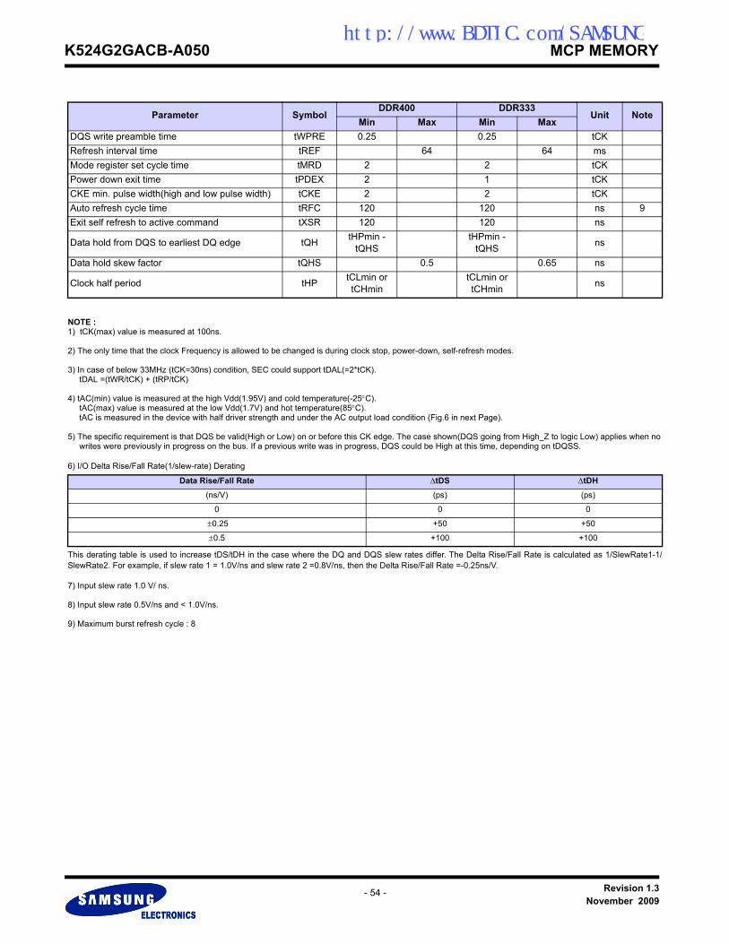
K524G2GACB-A050 MCP MEMORYhttp://www.BDTIC.com/SAMSUNG
NOTE :1) tCK(max) value is measured at 100ns.
2) The only time that the clock Frequency is allowed to be changed is during clock stop, power-down, self-refresh modes.
3) In case of below 33MHz (tCK=30ns) condition, SEC could support tDAL(=2*tCK). tDAL =(tWR/tCK) + (tRP/tCK)
4) tAC(min) value is measured at the high Vdd(1.95V) and cold temperature(-25°C). tAC(max) value is measured at the low Vdd(1.7V) and hot temperature(85°C). tAC is measured in the device with half driver strength and under the AC output load condition (Fig.6 in next Page).
5) The specific requirement is that DQS be valid(High or Low) on or before this CK edge. The case shown(DQS going from High_Z to logic Low) applies when no writes were previously in progress on the bus. If a previous write was in progress, DQS could be High at this time, depending on tDQSS.
6) I/O Delta Rise/Fall Rate(1/slew-rate) Derating
This derating table is used to increase tDS/tDH in the case where the DQ and DQS slew rates differ. The Delta Rise/Fall Rate is calculated as 1/SlewRate1-1/SlewRate2. For example, if slew rate 1 = 1.0V/ns and slew rate 2 =0.8V/ns, then the Delta Rise/Fall Rate =-0.25ns/V.
7) Input slew rate 1.0 V/ ns. 8) Input slew rate 0.5V/ns and < 1.0V/ns.
9) Maximum burst refresh cycle : 8
Parameter SymbolDDR400 DDR333
Unit NoteMin Max Min Max
DQS write preamble time tWPRE 0.25 0.25 tCKRefresh interval time tREF 64 64 msMode register set cycle time tMRD 2 2 tCKPower down exit time tPDEX 2 1 tCKCKE min. pulse width(high and low pulse width) tCKE 2 2 tCKAuto refresh cycle time tRFC 120 120 ns 9Exit self refresh to active command tXSR 120 120 ns
Data hold from DQS to earliest DQ edge tQH tHPmin - tQHS
tHPmin - tQHS ns
Data hold skew factor tQHS 0.5 0.65 ns
Clock half period tHP tCLmin or tCHmin
tCLmin ortCHmin ns
Data Rise/Fall Rate ∆tDS ∆tDH(ns/V) (ps) (ps)
0 0 0
±0.25 +50 +50
±0.5 +100 +100
Revision 1.3November 2009
- 54 -

K524G2GACB-A050 MCP MEMORYhttp://www.BDTIC.com/SAMSUNG
8. AC Operating Test Conditions (VDD = 1.7V to 1.95V, TC = -25°C to 85°C)
Figure 5. DC Output Load Circuit
Figure 6. AC Output Load Circuit 1), 2)
NOTE :1) The circuit shown above represents the timing reference load used in defining the relevant timing parameters of the part. It is not intended to be either a preciserepresentation of the typical system environment nor a depiction of the actual load presented by a production tester. System designers will used IBIS or other sim-ulations tools to correlate the timing reference load to system environment. Manufacturers will correlate to their poduction test conditions (generally a coaxial trans-mission line terminated at the tester electronics). For the half strength driver with a nominal 10pF load parameters tAC and tQH are expected to be in ther samerange. However, these parameters are not subject to production test but are estimated by design / characterization. Use of IBIS or other simulation tolls for systemdesign validation is suggested.
2) Based on nominal impedance at 0.5 x VDDQ.The impedence for Half(1/2) Driver Strength is designed 55ohm. And for other Driver Strength, it is designed proportionally.
Parameter Value Unit
AC input levels (Vih/Vil) 0.8 x VDDQ / 0.2 x VDDQ V
Input timing measurement reference level 0.5 x VDDQ V
Input signal minimum slew rate 1.0 V/ns
Output timing measurement reference level 0.5 x VDDQ V
Output load condition See Figure 6
1.8V
13.9KΩ
10.6KΩ
Output
20pF
- VOH (DC) = 0.9 x VDDQ, IOH = -0.1mA - VOL (DC) = 0.1 x VDDQ, IOL = 0.1mA
Vtt=0.5 x VDDQ
50Ω
Output Z0=50Ω Test load values need to be proportional to the driver strength which is set by the controller. - Test load for Full Driver Strength Buffer (20pF) - Test load for Half Driver Strength Buffer (10pF)
Revision 1.3November 2009
- 55 -

K524G2GACB-A050 MCP MEMORYhttp://www.BDTIC.com/SAMSUNG
9. Input/Output Capacitance(VDD=1.8, VDDQ=1.8V, TC = 25°C, f=100MHz)
Parameter Symbol Min Max Unit
Input capacitance(A0 ~ A13, BA0 ~ BA1, CKE, CS, RAS,CAS, WE) CIN1 1.5 3.0 pF
Input capacitance( CK, CK ) CIN2 1.5 3.5 pF
Data & DQS input/output capacitance COUT 2.0 4.5 pF
Input capacitance(DM) CIN3 2.0 4.5 pF
Revision 1.3November 2009
- 56 -

K524G2GACB-A050 MCP MEMORYhttp://www.BDTIC.com/SAMSUNG
10. AC Overshoot/Undershoot Specification for Address & Control Pins
Figure 7. AC Overshoot and Undershoot Definition for Address and Control Pins
11. AC Overshoot/Undershoot Specification for CLK, DQ, DQS and DM Pins
Figure 8. AC Overshoot and Undershoot Definition for CLK, DQ, DQS and DM Pins
Parameter Specification
Maximum peak Amplitude allowed for overshoot area 0.9V
Maximum peak Amplitude allowed for undershoot area 0.9V
Maximum overshoot area above VDD 3V-ns
Maximum undershoot area below VSS 3V-ns
Parameter Specification
Maximum peak Amplitude allowed for overshoot area 0.9V
Maximum peak Amplitude allowed for undershoot area 0.9V
Maximum overshoot area above VDDQ 3V-ns
Maximum undershoot area below VSSQ 3V-ns
Overshoot AreaMaximum Amplitude
VDD
Undershoot AreaMaximum Amplitude
VSS
Volts(V)
Time (ns)
Overshoot AreaMaximum Amplitude
VDDQ
Undershoot AreaMaximum Amplitude
VSSQ
Volts(V)
Time (ns)
Revision 1.3November 2009
- 57 -
K524G2GACB-A050 MCP MEMORYhttp://www.BDTIC.com/SAMSUNG
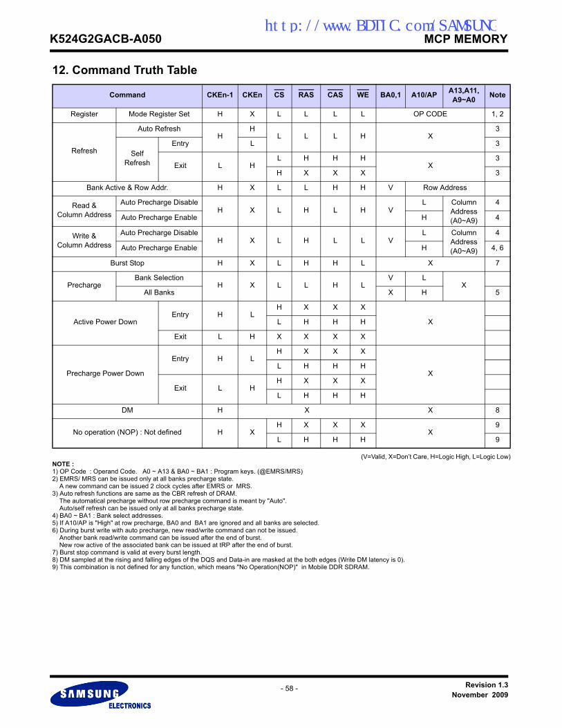
12. Command Truth Table
(V=Valid, X=Don’t Care, H=Logic High, L=Logic Low)NOTE :1) OP Code : Operand Code. A0 ~ A13 & BA0 ~ BA1 : Program keys. (@EMRS/MRS)2) EMRS/ MRS can be issued only at all banks precharge state. A new command can be issued 2 clock cycles after EMRS or MRS.3) Auto refresh functions are same as the CBR refresh of DRAM. The automatical precharge without row precharge command is meant by "Auto". Auto/self refresh can be issued only at all banks precharge state.4) BA0 ~ BA1 : Bank select addresses.5) If A10/AP is "High" at row precharge, BA0 and BA1 are ignored and all banks are selected.6) During burst write with auto precharge, new read/write command can not be issued. Another bank read/write command can be issued after the end of burst. New row active of the associated bank can be issued at tRP after the end of burst.7) Burst stop command is valid at every burst length.8) DM sampled at the rising and falling edges of the DQS and Data-in are masked at the both edges (Write DM latency is 0). 9) This combination is not defined for any function, which means "No Operation(NOP)" in Mobile DDR SDRAM.
Command CKEn-1 CKEn CS RAS CAS WE BA0,1 A10/AP A13,A11,A9~A0 Note
Register Mode Register Set H X L L L L OP CODE 1, 2
Refresh
Auto RefreshH
HL L L H X
3
Self Refresh
Entry L 3
Exit L HL H H H
X3
H X X X 3
Bank Active & Row Addr. H X L L H H V Row Address
Read &Column Address
Auto Precharge DisableH X L H L H V
L ColumnAddress(A0~A9)
4
Auto Precharge Enable H 4
Write &Column Address
Auto Precharge DisableH X L H L L V
L ColumnAddress(A0~A9)
4
Auto Precharge Enable H 4, 6
Burst Stop H X L H H L X 7
PrechargeBank Selection
H X L L H LV L
XAll Banks X H 5
Active Power DownEntry H L
H X X X
XL H H H
Exit L H X X X X
Precharge Power Down
Entry H LH X X X
XL H H H
Exit L HH X X X
L H H H
DM H X X 8
No operation (NOP) : Not defined H XH X X X
X9
L H H H 9
Revision 1.3November 2009
- 58 -
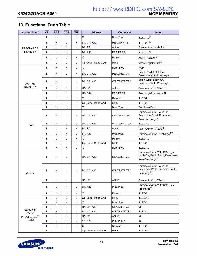
K524G2GACB-A050 MCP MEMORYhttp://www.BDTIC.com/SAMSUNG
13. Functional Truth Table Current State CS RAS CAS WE Address Command Action
PRECHARGESTANDBY
L H H L X Burst Stop ILLEGAL2)
L H L X BA, CA, A10 READ/WRITE ILLEGAL2)
L L H H BA, RA Active Bank Active, Latch RA
L L H L BA, A10 PRE/PREA ILLEGAL4)
L L L H X Refresh AUTO-Refresh5)
L L L L Op-Code, Mode-Add MRS Mode Register Set5)
ACTIVESTANDBY
L H H L X Burst Stop NOP
L H L H BA, CA, A10 READ/READA Begin Read, Latch CA,Determine Auto-Precharge
L H L L BA, CA, A10 WRITE/WRITEA Begin Write, Latch CA,Determine Auto-Precharge
L L H H BA, RA Active Bank Active/ILLEGAL2)
L L H L BA, A10 PRE/PREA Precharge/Precharge All
L L L H X Refresh ILLEGAL
L L L L Op-Code, Mode-Add MRS ILLEGAL
READ
L H H L X Burst Stop Terminate Burst
L H L H BA, CA, A10 READ/READATerminate Burst, Latch CA,Begin New Read, DetermineAuto-Precharge3)
L H L L BA, CA, A10 WRITE/WRITEA ILLEGAL
L L H H BA, RA Active Bank Active/ILLEGAL2)
L L H L BA, A10 PRE/PREA Terminate Burst, Precharge10)
L L L H X Refresh ILLEGAL
L L L L Op-Code, Mode-Add MRS ILLEGAL
WRITE
L H H L X Burst Stop ILLEGAL
L H L H BA, CA, A10 READ/READA
Terminate Burst With DM=High, Latch CA, Begin Read, Determine Auto-Precharge3)
L H L L BA, CA, A10 WRITE/WRITEA
Terminate Burst, Latch CA, Begin new Write, Determine Auto-Precharge3)
L L H H BA, RA Active Bank Active/ILLEGAL2)
L L H L BA, A10 PRE/PREATerminate Burst With DM=High,Precharge10)
L L L H X Refresh ILLEGAL
L L L L Op-Code, Mode-Add MRS ILLEGAL
READ withAUTO
PRECHARGE6)
(READA)
L H H L X Burst Stop ILLEGAL
L H L H BA, CA, A10 READ/READA 6)
L H L L BA, CA, A10 WRITE/WRITEA ILLEGAL
L L H H BA, RA Active 6)
L L H L BA, A10 PRE/PREA 6)
L L L H X Refresh ILLEGAL
L L L L Op-Code, Mode-Add MRS ILLEGAL
Revision 1.3November 2009
- 59 -
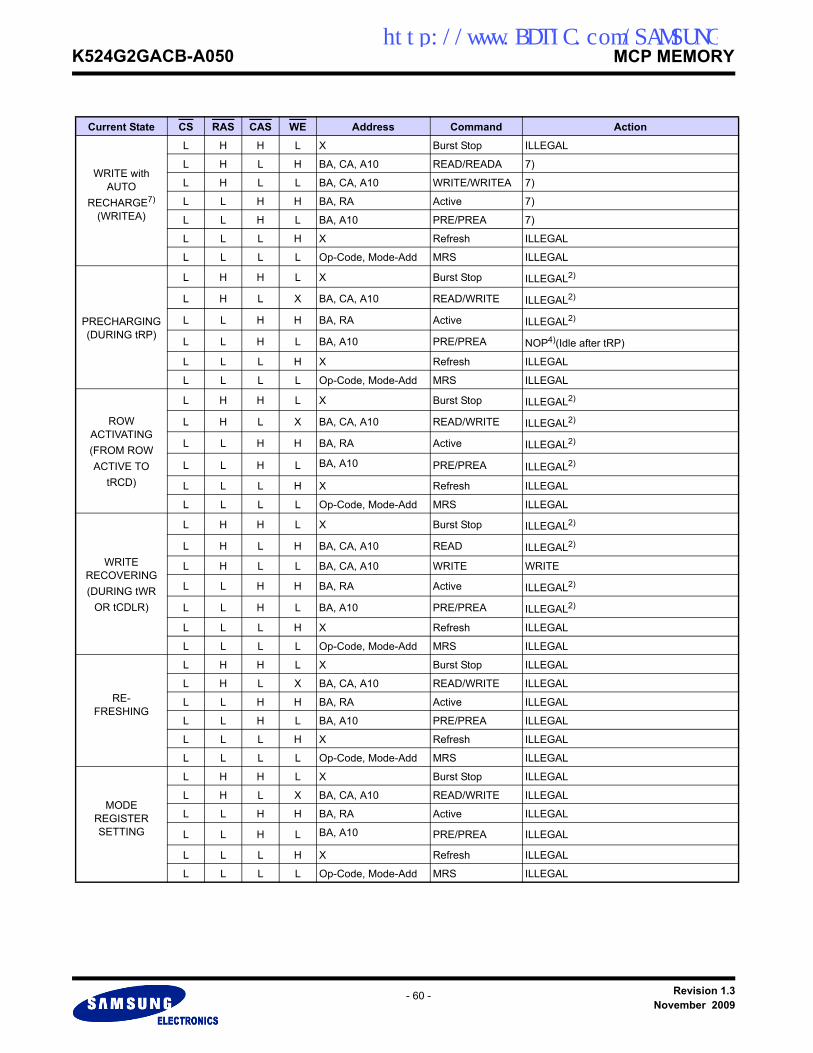
K524G2GACB-A050 MCP MEMORYhttp://www.BDTIC.com/SAMSUNG
Current State CS RAS CAS WE Address Command Action
WRITE with AUTO
RECHARGE7)
(WRITEA)
L H H L X Burst Stop ILLEGAL
L H L H BA, CA, A10 READ/READA 7)
L H L L BA, CA, A10 WRITE/WRITEA 7)
L L H H BA, RA Active 7)
L L H L BA, A10 PRE/PREA 7)
L L L H X Refresh ILLEGAL
L L L L Op-Code, Mode-Add MRS ILLEGAL
PRECHARGING(DURING tRP)
L H H L X Burst Stop ILLEGAL2)
L H L X BA, CA, A10 READ/WRITE ILLEGAL2)
L L H H BA, RA Active ILLEGAL2)
L L H L BA, A10 PRE/PREA NOP4)(Idle after tRP)
L L L H X Refresh ILLEGAL
L L L L Op-Code, Mode-Add MRS ILLEGAL
ROWACTIVATING(FROM ROWACTIVE TO
tRCD)
L H H L X Burst Stop ILLEGAL2)
L H L X BA, CA, A10 READ/WRITE ILLEGAL2)
L L H H BA, RA Active ILLEGAL2)
L L H L BA, A10 PRE/PREA ILLEGAL2)
L L L H X Refresh ILLEGAL
L L L L Op-Code, Mode-Add MRS ILLEGAL
WRITE RECOVERING(DURING tWR
OR tCDLR)
L H H L X Burst Stop ILLEGAL2)
L H L H BA, CA, A10 READ ILLEGAL2)
L H L L BA, CA, A10 WRITE WRITE
L L H H BA, RA Active ILLEGAL2)
L L H L BA, A10 PRE/PREA ILLEGAL2)
L L L H X Refresh ILLEGAL
L L L L Op-Code, Mode-Add MRS ILLEGAL
RE-FRESHING
L H H L X Burst Stop ILLEGAL
L H L X BA, CA, A10 READ/WRITE ILLEGAL
L L H H BA, RA Active ILLEGAL
L L H L BA, A10 PRE/PREA ILLEGAL
L L L H X Refresh ILLEGAL
L L L L Op-Code, Mode-Add MRS ILLEGAL
MODEREGISTERSETTING
L H H L X Burst Stop ILLEGAL
L H L X BA, CA, A10 READ/WRITE ILLEGAL
L L H H BA, RA Active ILLEGAL
L L H L BA, A10 PRE/PREA ILLEGAL
L L L H X Refresh ILLEGAL
L L L L Op-Code, Mode-Add MRS ILLEGAL
Revision 1.3November 2009
- 60 -

K524G2GACB-A050 MCP MEMORYhttp://www.BDTIC.com/SAMSUNG
(H=High Level, L=Low level, X=Don′t Care)
NOTE :1) All entries assume that CKE was High during the preceding clock cycle and the current clock cycle.2) ILLEGAL to bank in specified state ; function may be legal in the bank indicated by BA, depending on the state of that bank. (ILLEGAL = Device operation and/or data integrity are not guaranteed.)3) Must satisfy bus contention, bus turn around and write recovery requirements.4) NOP to bank precharging or in idle sate. May precharge bank indicated by BA.5) ILLEGAL if any bank is not idle.6) Refer to "Read with Auto Precharge Timing Diagram" for detailed information.7) Refer to "Write with Auto Precharge Timing Diagram" for detailed information.8) CKE Low to High transition will re-enable CK, CK and other inputs asynchronously. A minimum setup time must be satisfied before issuing any command other than EXIT.9) Power-Down, Self-Refresh can be entered only from All Bank Idle state.
Current State CKEn-1
CKEn CS RAS CAS WE Add Action
SELF-REFRESHING8)
L H H X X X X Exit Self-Refresh
L H L H H H X Exit Self-Refresh
L H L H H L X ILLEGAL
L H L H L X X ILLEGAL
L H L L X X X ILLEGAL
L L X X X X X NOP (Maintain Self-Refresh)
POWERDOWN
L H X X X X X Exit Power Down(Idle after tPDEX)
L L X X X X X NOP (Maintain Power Down)
ALL BANKS
IDLE9)
H H X X X X X Refer to Function Truth Table
H L L L L H X Enter Self-Refresh
H L H X X X X Enter Power Down
H L L H H H X Enter Power Down
H L L H H L X ILLEGAL
H L L H L X X ILLEGAL
H L L L X X X ILLEGAL
L X X X X X X Refer to Current State=Power Down
Revision 1.3November 2009
- 61 -

K524G2GACB-A050 MCP MEMORYhttp://www.BDTIC.com/SAMSUNG
MOBILE DDR SDRAM
Device Operations & Timing Diagram
Revision 1.3November 2009
- 62 -

K524G2GACB-A050 MCP MEMORYhttp://www.BDTIC.com/SAMSUNG
Device Operations
Revision 1.3November 2009
- 63 -

K524G2GACB-A050 MCP MEMORYhttp://www.BDTIC.com/SAMSUNG
1. PrechargeThe precharge command is used to precharge or close a bank that has been activated. The precharge command is issued when CS, RAS andWE are low and CAS is high at the rising edge of the clock. The precharge command can be used to precharge each bank respectively or allbanks simultaneously. The bank select addresses(BA0, BA1) are used to define which bank is precharged when the command is initiated.For write cycle, tWR(min.) must be satisfied until the precharge command can be issued. After tRP from the precharge, an active command tothe same bank can be initiated.
Table 1. Bank selection for precharge by Bank address bits
2. No Operation(NOP) & Device DeselectThe device should be deselected by deactivating the CS signal. In this mode, Mobile DDR SDRAM should ignore all the control inputs. The Mobile DDR SDRAM is put in NOP mode when CS is activated and RAS, CAS and WE are deactivated. Both Device Deselect and NOP com-mand can not affect operation already in progress. So even if the device is deselected or NOP command is issued under operation, the oper-ation will be completed.
A10/AP BA1 BA0 Precharge
0 0 0 Bank A Only
0 0 1 Bank B Only
0 1 0 Bank C Only
0 1 1 Bank D Only
1 X X All Banks
Revision 1.3November 2009
- 64 -
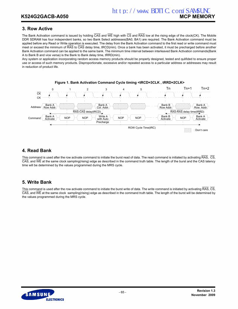
K524G2GACB-A050 MCP MEMORYhttp://www.BDTIC.com/SAMSUNG
3. Row ActiveThe Bank Activation command is issued by holding CAS and WE high with CS and RAS low at the rising edge of the clock(CK). The MobileDDR SDRAM has four independent banks, so two Bank Select addresses(BA0, BA1) are required. The Bank Activation command must beapplied before any Read or Write operation is executed. The delay from the Bank Activation command to the first read or write command mustmeet or exceed the minimum of RAS to CAS delay time, tRCD(min). Once a bank has been activated, it must be precharged before anotherBank Activation command can be applied to the same bank. The minimum time interval between interleaved Bank Activation commands(BankA to Bank B and vice versa) is the Bank to Bank delay time, tRRD(min).Any system or application incorporating random access memory products should be properly designed, tested and qulifided to ensure properuse or access of such memory products. Disproportionate, excessive and/or repeated access to a particular address or addresses may resultin reduction of product life.
Figure 1. Bank Activation Command Cycle timing <tRCD=3CLK , tRRD=2CLK>
4. Read BankThis command is used after the row activate command to initiate the burst read of data. The read command is initiated by activating RAS, CS, CAS, and WE at the same clock sampling(rising) edge as described in the command truth table. The length of the burst and the CAS latency time will be determined by the values programmed during the MRS cycle.
5. Write BankThis command is used after the row activate command to initiate the burst write of data. The write command is initiated by activating RAS, CS, CAS, and WE at the same clock sampling(rising) edge as described in the command truth table. The length of the burst will be determined by the values programmed during the MRS cycle.
Address
Command
RAS-CAS delay(tRCD)
Bank ARow Addr.
Bank ACol. Addr.
Bank AActivate
Write Awith Auto NOP
Precharge
RAS-RAS delay time(tRRD)
Bank BRow Addr.
Bank ARow. Addr.
Bank BActivate
Bank AActivateNOP
ROW Cycle Time(tRC)
Tn Tn+1 Tn+220 1
: Don′t care
CKCK
53 4
NOP NOPNOP
Revision 1.3November 2009
- 65 -
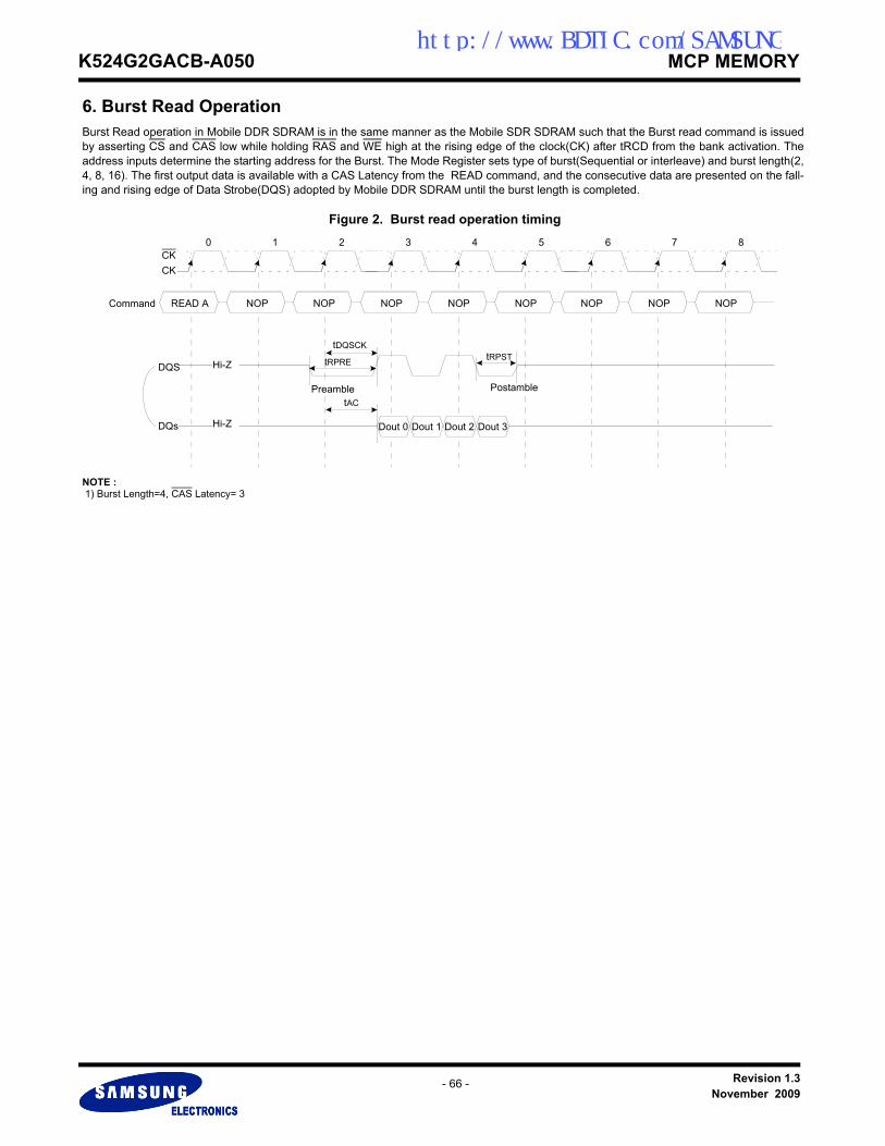
K524G2GACB-A050 MCP MEMORYhttp://www.BDTIC.com/SAMSUNG
6. Burst Read OperationBurst Read operation in Mobile DDR SDRAM is in the same manner as the Mobile SDR SDRAM such that the Burst read command is issuedby asserting CS and CAS low while holding RAS and WE high at the rising edge of the clock(CK) after tRCD from the bank activation. Theaddress inputs determine the starting address for the Burst. The Mode Register sets type of burst(Sequential or interleave) and burst length(2,4, 8, 16). The first output data is available with a CAS Latency from the READ command, and the consecutive data are presented on the fall-ing and rising edge of Data Strobe(DQS) adopted by Mobile DDR SDRAM until the burst length is completed.
Figure 2. Burst read operation timing
NOTE : 1) Burst Length=4, CAS Latency= 3
Command READ A NOP NOP NOP NOPNOP NOP NOPNOP
20 1 53 4 86 7
DQS
DQs Dout 0 Dout 1 Dout 2 Dout 3
tRPSTtRPRE
Preamble Postamble
CKCK
tDQSCK
tAC
Hi-Z
Hi-Z
Revision 1.3November 2009
- 66 -

K524G2GACB-A050 MCP MEMORYhttp://www.BDTIC.com/SAMSUNG
7. Burst Write OperationThe Burst Write command is issued by having CS, CAS, and WE low while holding RAS high at the rising edge of the clock(CK). The addressinputs determine the starting column address. There is no write latency relative to DQS required for burst write cycle. The first data of a burstwrite cycle must be applied on the DQ pins tDS(Data-in setup time) prior to data strobe edge enabled after tDQSS from the rising edge of theclock(CK) that the write command is issued. The remaining data inputs must be supplied on each subsequent falling and rising edge of DataStrobe until the burst length is completed. When the burst has been finished, any additional data supplied to the DQ pins will be ignored.
Figure 3. Burst write operation timing
NOTE : 1) Burst Length=4 2) The specific requirement is that DQS be valid(High or Low) on or before this CK edge. The case shown (DQS going from High_Z to logic Low) applies when no writes were previously in progress on the bus.
Command
tWR
tWRtDQSS(min)
tDQSS(max)
20 1 53 4 86 7
tWPREStWPREH
tWPRES tWPREH
CKCK
Din 3Din 0 Din 1 Din 2 Din 3Din 0 Din 1 Din 2
Din 3Din 0 Din 1 Din 2 Din 3Din 0 Din 1 Din 2
NOP WRITEA NOP NOP NOPWRITEB NOP NOPNOP
tDS tDH
Hi-Z
Hi-Z
Hi-Z
Hi-Z
tDQSS(max)
tDQSS(min)
DQS
DQs
DQS
DQs
Revision 1.3November 2009
- 67 -
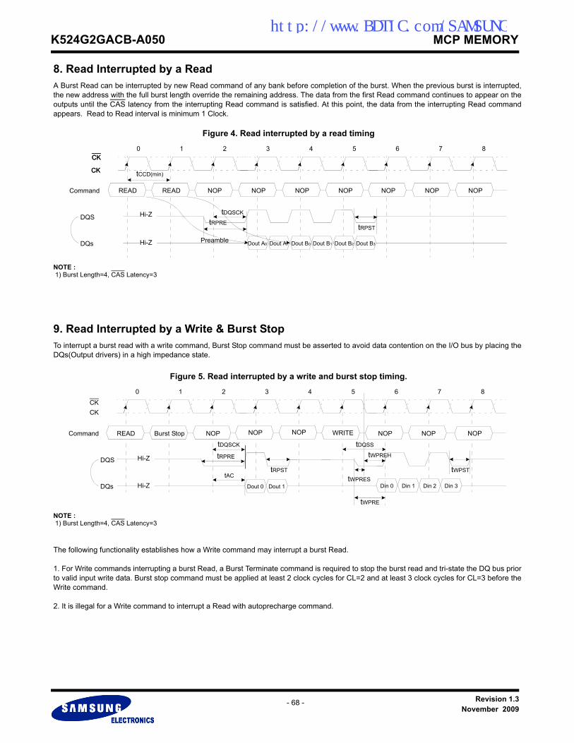
K524G2GACB-A050 MCP MEMORYhttp://www.BDTIC.com/SAMSUNG
8. Read Interrupted by a ReadA Burst Read can be interrupted by new Read command of any bank before completion of the burst. When the previous burst is interrupted,the new address with the full burst length override the remaining address. The data from the first Read command continues to appear on theoutputs until the CAS latency from the interrupting Read command is satisfied. At this point, the data from the interrupting Read commandappears. Read to Read interval is minimum 1 Clock.
Figure 4. Read interrupted by a read timing
NOTE : 1) Burst Length=4, CAS Latency=3
9. Read Interrupted by a Write & Burst StopTo interrupt a burst read with a write command, Burst Stop command must be asserted to avoid data contention on the I/O bus by placing theDQs(Output drivers) in a high impedance state.
Figure 5. Read interrupted by a write and burst stop timing.
NOTE : 1) Burst Length=4, CAS Latency=3
The following functionality establishes how a Write command may interrupt a burst Read.
1. For Write commands interrupting a burst Read, a Burst Terminate command is required to stop the burst read and tri-state the DQ bus priorto valid input write data. Burst stop command must be applied at least 2 clock cycles for CL=2 and at least 3 clock cycles for CL=3 before theWrite command.
2. It is illegal for a Write command to interrupt a Read with autoprecharge command.
Command READ READ NOP NOP NOPNOP NOP NOPNOP
DQS
DQs Dout A0 Dout A1 Dout B0 Dout B1 Dout B2 Dout B3
CK
20 1 53 4 86 7
tRPRE
Preamble
tDQSCK
CK
CK
CK
tCCD(min)
tRPST
Hi-Z
Hi-Z
Command READ Burst Stop NOP WRITENOP NOP NOP
DQS
DQs Dout 0 Dout 1 Din 0 Din 1 Din 2 Din 3
20 1 53 4 86 7
NOP
tWPREH
tWPRES
tRPRE
tDQSStDQSCK
tAC
CKCK
NOP
tWPST
Hi-Z
Hi-Z
tWPRE
tRPST
Revision 1.3November 2009
- 68 -

K524G2GACB-A050 MCP MEMORYhttp://www.BDTIC.com/SAMSUNG
10. Read Interrupted by a PrechargeA Burst Read operation can be interrupted by precharge of the same bank. The minimum 1 clock is required for the read to precharge inter-vals. The latency from a precharge command to invalid output is equivalent to the CAS latency.
Figure 6. Read interrupted by a precharge timing
NOTE : 1) Burst Length=8, CAS Latency=3
When a burst Read command is issued to a Mobile DDR SDRAM, a Precharge command may be issued to the same bank before the Readburst is completed. The following functionality determines when a Precharge command may be given during a Read burst and when a newBank Activate command may be issued to the same bank.
1. For the earliest possible Precharge command without interrupting a burst Read, the Precharge command may be given on the rising clockedge which is CL clock cycles before the end of the Read burst where CL is the CAS Latency. A new Bank Activate command may be issuedto the same bank after tRP (Row Precharge time).
2. When a Precharge command interrupts a burst Read operation, the Precharge command given on a rising clock edge terminates the burstwith the last valid data word presented on DQ pins at CL-1(CL=CAS Latency) clock cycles after the command has been issued. Once thelast data word has been output, the output buffers are tri-stated. A new Bank Activate command may be issued to the same bank after tRP.
3. For a Read with Autoprecharge command, a new Bank Activate command may be issued to the same bank after tRP from rising clock thatcomes CL(CL=CAS Latency) clock cycles before the end of the Read burst. During Read with autoprecharge, the initiation of the internalprecharge occurs at the same time as the earliest possible external Precharge command would initiate a precharge operation withoutinterrupting the Read burst as described in 1 above.
4. For all cases above, tRP is an analog delay that needs to be converted into clock cycles. The number of clock cycles between a Prechargecommand and a new Bank Activate command to the same bank equals tRP/tCK (where tCK is the clock cycle time) with the result roundedup to the nearest integer number of clock cycles. (Note that rounding to X.5 is not possible since the Precharge and Bank Activatecommands can only be given on a rising clock edge).In all cases, a Precharge operation cannot be initiated unless tRAS(min) [minimumBank Activate to Precharge time] has been satisfied. This includes Read with autoprecharge commands where tRAS(min) must still besatisfied such that a Read with autoprecharge command has the same timing as a Read command followed by the earliest possiblePrecharge command which does not interrupt the burst.
Command READ NOPPrecharge NOP NOPNOP NOP NOPNOP
DQS
DQs Dout 0 Dout 1 Dout 2 Dout 3
Interrupted by precharge
20 1 53 4 86 7
Dout 4 Dout 5 Dout 6 Dout 7
1tCK
tRPRE
tDQSCK
tAC
CKCK
Hi-Z
Hi-Z
Revision 1.3November 2009
- 69 -

K524G2GACB-A050 MCP MEMORYhttp://www.BDTIC.com/SAMSUNG
11. Write Interrupted by a WriteA Burst Write can be interrupted by a new Write command before completion of the burst, where the interval between the successive Writecommands must be at least one clock cycle(tCCD(min)). When the previous burst is interrupted, the remaining addresses are overridden bythe new address and data will be written into the device until the programmed burst length is satisfied.
Figure 7. Write interrupted by a write timing
NOTE : 1) Burst Length=4
Command NOP WRITE A WRITE b NOP NOPNOP NOP NOPNOP
DQS
DQs Din A0 Din A1 Din B0 Din B1 Din B2 Din B3
tCCD(min)
20 1 53 4 86 7CKCK
Hi-Z
Hi-Z
Revision 1.3November 2009
- 70 -

K524G2GACB-A050 MCP MEMORYhttp://www.BDTIC.com/SAMSUNG
12. Write Interrupted by a Precharge & DMA burst write operation can be interrupted by a precharge of the same bank before completion of the burst. Random column access is allowed.A write recovery time(tWR) is required from the last data to precharge command. When precharge command is asserted, any residual datafrom the burst write cycle must be masked by DM.
Figure 8. Write interrupted by a precharge and DM timing
NOTE : 1) Burst Length=8
Precharge timing for Write operations in Mobile DDR SDRAM requires enough time to allow ’’write recovery’’ which is the time required by aMobile DDR SDRAM core to properly store a full ’’0’’ or ’’1’’ level before a Precharge operation. For Mobile DDR SDRAM, a timing parameter,tWR, is used to indicate the required amount of time between the last valid write operation and a Precharge command to the same bank.
The precharge timing for writes is a complex definition since the write data is sampled by the data strobe and the address is sampled by theinput clock. Inside the Mobile DDR SDRAM, the data path is eventually synchronized with the address path by switching clock domains fromthe data strobe clock domain to the input clock domain. This makes the definition of when a precharge operation can be initiated after a writevery complex since the write recovery parameter must make reference to only the clock domain that affects internal write operation, i.e., theinput clock domain.
tWR starts on the rising clock edge after the last possible DQS edge that strobed in the last valid data and ends on the rising clock edge thatstrobes in the precharge command.1. For the earliest possible Precharge command following a burst Write without interrupting the burst, the minimum time for write recovery is
defined by tWR.2. When a precharge command interrupts a Write burst operation, the data mask pin, DM, is used to mask input data during the time between
the last valid write data and the rising clock edge on which the Precharge command is given. During this time, the DQS input is stillrequired to strobe in the state of DM. The minimum time for write recovery is defined by tWR.
3. For a Write with autoprecharge command, a new Bank Activate command may be issued to the same bank after tWR+tRP where tWR+tRPstarts on the falling DQS edge that strobed in the last valid data and ends on the rising clock edge that strobes in the Bank Activatecommand. During write with autoprecharge, the initiation of the internal precharge occurs at the same time as the earliest possibleexternal Precharge command without interrupting the Write burst as described in 1 above.
4. In all cases, a Precharge operation cannot be initiated unless tRAS(min) [minimum Bank Activate to Precharge time] has been satisfied.This includes Write with autoprecharge commands where tRAS(min) must still be satisfied such that a Write with autoprechargecommand has the same timing as a Write command followed by the earliest possible Precharge command which does not interrupt theburst.
Dina2 Dina3
Command NOP WRITE A NOP NOP PrechargeANOP NOPWRITE B
DQS
DQsDina0 Dina1 Dina4 Dina5 Dinb0 Dinb1Dina6 Dina7
tWR
DQS
DQs
tWRtDQSS(min)
Dina0 Dina1 Dina2 Dina3 Dina4 Dina5 Dina6 Dina7
DM
Dinb0 Dinb1
tDQSS(max)
20 1 53 4 86 7
DM
tWPRES
tWPREH
tWPRES tWPREH
NOP
tDQSS(max)
tWPRES
tWPREH
tDQSS(min)
tWPRES tWPREH
Dinb2
CKCK
tDQSS(max)
tDQSS(min)
Hi-Z
Hi-Z
Hi-Z
Hi-Z
Revision 1.3November 2009
- 71 -

K524G2GACB-A050 MCP MEMORYhttp://www.BDTIC.com/SAMSUNG
13. Write Interrupted by a Read & DMA burst write can be interrupted by a read command of any bank. The DQ’s must be in the high impedance state at least one clock cyclebefore the interrupting read data appear on the outputs to avoid data contention. When the read command is registered, any residual datafrom the burst write cycle must be masked by DM. The delay from the last data to read command (tCDLR) is required to avoid the data con-tention Mobile DDR SDRAM inside. Data that are presented on the DQ pins before the read command is initiated will actually be written to thememory. Read command interrupting write can not be issued at the next clock edge of that of write command.
Figure 9. Write interrupted by a Read and DM timing
NOTE : 1) Burst Length=8, CAS Latency=3
The following function established how a Read command may interrupt a Write burst and which input data is not written into the memory.1. For Read commands interrupting a burst Write, the minimum Write to Read command delay is 2 clock cycles. The case where the Write to
Read delay is 1 clock cycle is disallowed.2. For Read commands interrupting a burst Write, the DM pin must be used to mask the input data words whcich immediately precede the
interrupting Read operation and the input data word which immediately follows the interrupting Read operation3. For all cases of a Read interrupting a Write, the DQ and DQS buses must be released by the driving chip (i.e., the memory controller) in
time to allow the buses to turn around before the Mobile DDR SDRAM drives them during a read operation.4. If input Write data is masked by the Read command, the DQS input is ignored by the Mobile DDR SDRAM.5. Refer to Burst write operation.
Command NOP WRITE NOP NOP READNOP NOP NOPNOP
Din 0 Din 1 Din 2 Din 3 Din 4 Din 5 Din 6 Din 7
tCDLRtDQSS(max)
tCDLRtDQSS(min)
Din 7Din 0 Din 1 Din 2 Din 3 Din 4 Din 5 Din 6
2 0 1 5 3 4 8 6 7
tWPRES5)
CKCK
DQS
DQs
DQS
DQs
DM
DM
DQSS(max)
DQSS(min)
NOP
Dout0 Dout1 Dout2 Dout3
Hi-Z
Hi-Z
Hi-Z
Hi-Z
Dout0 Dout1 Dout2 Dout3
9
Dout4
Dout4
NOP
tWPRES5)
Revision 1.3November 2009
- 72 -
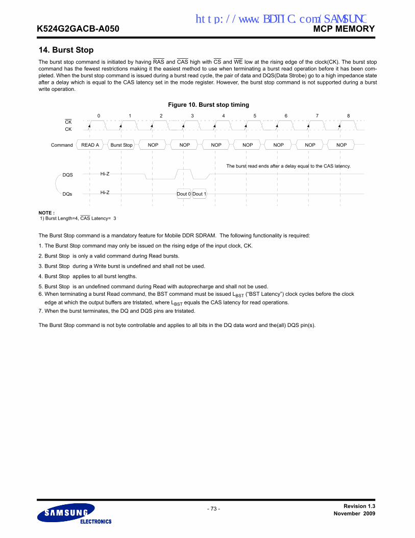
K524G2GACB-A050 MCP MEMORYhttp://www.BDTIC.com/SAMSUNG
14. Burst StopThe burst stop command is initiated by having RAS and CAS high with CS and WE low at the rising edge of the clock(CK). The burst stopcommand has the fewest restrictions making it the easiest method to use when terminating a burst read operation before it has been com-pleted. When the burst stop command is issued during a burst read cycle, the pair of data and DQS(Data Strobe) go to a high impedance stateafter a delay which is equal to the CAS latency set in the mode register. However, the burst stop command is not supported during a burstwrite operation.
Figure 10. Burst stop timing
NOTE : 1) Burst Length=4, CAS Latency= 3
The Burst Stop command is a mandatory feature for Mobile DDR SDRAM. The following functionality is required:
1. The Burst Stop command may only be issued on the rising edge of the input clock, CK.
2. Burst Stop is only a valid command during Read bursts.
3. Burst Stop during a Write burst is undefined and shall not be used.
4. Burst Stop applies to all burst lengths.
5. Burst Stop is an undefined command during Read with autoprecharge and shall not be used.6. When terminating a burst Read command, the BST command must be issued LBST (“BST Latency”) clock cycles before the clock edge at which the output buffers are tristated, where LBST equals the CAS latency for read operations. 7. When the burst terminates, the DQ and DQS pins are tristated.
The Burst Stop command is not byte controllable and applies to all bits in the DQ data word and the(all) DQS pin(s).
Command READ A Burst Stop NOP NOP NOPNOP NOP NOPNOP
DQS
DQs Dout 0 Dout 1
20 1 53 4 86 7
The burst read ends after a delay equal to the CAS latency.
CKCK
Hi-Z
Hi-Z
Revision 1.3November 2009
- 73 -

K524G2GACB-A050 MCP MEMORYhttp://www.BDTIC.com/SAMSUNG
15. DM maskingThe Mobile DDR SDRAM has a data mask function that can be used in conjunction with data write cycle, not read cycle. When the data maskis activated(DM high) during write operation, Mobile DDR SDRAM does not accept the corresponding data.(DM to data-mask latency is zero).DM must be issued at the rising or falling edge of data strobe.
Figure 11. DM masking timing
NOTE : 1) Burst Length=8
Command WRITE NOP NOP NOP NOPNOP NOP NOPNOP
DQS
DQs Din 0 Din 1 Din 2 Din 3
DM
Din 4 Din 5 Din 6 Din7
masked by DM=H
20 1 53 4 86 7
tDQSS
tWPRES tWPREH
CKCK
Hi-Z
Hi-Z
Revision 1.3November 2009
- 74 -

K524G2GACB-A050 MCP MEMORYhttp://www.BDTIC.com/SAMSUNG
16. Read With Auto PrechargeIf A10/AP is high when read command is issued , the read with auto-precharge function is performed. If a read with auto-precharge commandis issued, the Mobile DDR SDRAM automatically enters the precharge operation BL/2 clock later from a read with auto-precharge commandwhen tRAS(min) is satisfied. If not, the start point of precharge operation will be delayed until tRAS(min) is satisfied. Once the prechargeoperation has started, the bank cannot be reactivated and the new command can not be asserted until the precharge time(tRP) has been sat-isfied.
Figure 12. Read with auto precharge timing
NOTE : 1) Burst Length=4, CAS Latency= 3 2) The row active command of the precharge bank can be issued after tRP from this point.
NOTE : 1) AP = Auto Precharge
Asserted command
For same Bank For Different Bank
5 6 7 5 6 7
READ READ +No AP1) READ+No AP Illegal Legal Legal Legal
READ+AP READ + AP READ + AP Illegal Legal Legal Legal
Active Illegal Illegal Illegal Legal Legal Legal
Precharge Legal Legal Illegal Legal Legal Legal
CommandBANK A NOP READ A NOP NOP NOPNOPACTIVE Auto Precharge
DQS
DQs Dout0Dout1Dout2Dout3
NOP
tRP Bank can be reactivated at
NOP NOP NOP NOP
tRAS(min)Auto-Precharge starts
CKCK
completion of tRP1) Hi-Z
Hi-Z
20 1 53 4 86 7 9 10 11
Revision 1.3November 2009
- 75 -

K524G2GACB-A050 MCP MEMORYhttp://www.BDTIC.com/SAMSUNG
17. Write with Auto PrechargeIf A10/AP is high when write command is issued , the write with auto-precharge function is performed. Any new command to the same bankshould not be issued until the internal precharge is completed. The internal precharge begins after keeping tWR(min).
Figure 13. Write with auto precharge timing
NOTE : 1) Burst Length=4 2) The row active command of the precharge bank can be issued after tRP from this point.
NOTE : 1) AP = Auto Precharge 2) DM : Refer to "27. Write Interrupted by Precharge & DM ".
Asserted command
For same Bank For Different Bank
5 6 7 8 9 10 5 6 7 8 9
WRITE WRITE+No AP1)
WRITE+No AP Illegal Illegal Illegal Illegal Legal Legal Legal Legal Legal
WRITE+AP
WRITE+AP
WRITE+AP Illegal Illegal Illegal Illegal Legal Legal Legal Legal Legal
READ IllegalREAD+
NO AP+DM2) READ+
NO AP+DMREAD+NO AP Illegal Illegal Illegal Illegal Illegal Legal Legal
READ+AP Illegal READ + AP+DM
READ + AP+DM
READ + AP Illegal Illegal Illegal Illegal Illegal Legal Legal
Active Illegal Illegal Illegal Illegal Illegal Illegal Legal Legal Legal Legal Legal
Precharge Illegal Illegal Illegal Illegal Illegal Illegal Legal Legal Legal Legal Legal
CommandBANK A NOP WRITE A NOP NOP NOPNOPACTIVE Auto Precharge
20 1 53 4 86 7
DQS
DQs Din 0 Din 1 Din 2 Din 3
NOP
tRP
NOP NOP NOP
9 10 11
tWR
Internal precharge start 1)
CKCK
Bank can be reactivated at completion of tRP
Hi-Z
Hi-Z
NOP NOPNOP
12 13
Revision 1.3November 2009
- 76 -
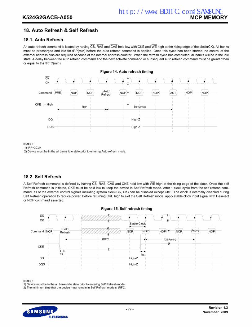
K524G2GACB-A050 MCP MEMORYhttp://www.BDTIC.com/SAMSUNG
18. Auto Refresh & Self Refresh
18.1. Auto RefreshAn auto refresh command is issued by having CS, RAS and CAS held low with CKE and WE high at the rising edge of the clock(CK). All banksmust be precharged and idle for tRP(min) before the auto refresh command is applied. Once this cycle has been started, no control of theexternal address pins are required because of the internal address counter. When the refresh cycle has completed, all banks will be in the idlestate. A delay between the auto refresh command and the next activate command or subsequent auto refresh command must be greater thanor equal to the tRFC(min).
Figure 14. Auto refresh timing
NOTE : 1) tRP=3CLK 2) Device must be in the all banks idle state prior to entering Auto refresh mode.
18.2. Self RefreshA Self Refresh command is defined by having CS, RAS, CAS and CKE held low with WE high at the rising edge of the clock. Once the selfRefresh command is initiated, CKE must be held low to keep the device in Self Refresh mode. After 1 clock cycle from the self refresh com-mand, all of the external control signals including system clock(CK, CK) can be disabled except CKE. The clock is internally disabled duringSelf Refresh operation to reduce power. Before returning CKE high to exit the Self Refresh mode, apply stable clock input signal with Deselector NOP command asserted.
Figure 15. Self refresh timing
NOTE :1) Device must be in the all banks idle state prior to entering Self Refresh mode.2) The minimum time that the device must remain in Self Refresh mode si tRFC.
Command
CKE
PRE
tRP tRFC(min)
Auto
= High
RefreshNOP
∼ ∼
CKCK
∼ ∼∼ ∼
NOP NOP NOP NOP NOP NOPACT
∼ ∼
DQ High-Z
DQS High-Z
Command
CKE
Stable Clock
tIS
NOPSelf
Refresh
tXSR(min)
tIS
∼∼∼∼
∼∼
Active
CKCK
NOP NOP NOP NOPNOP
∼∼∼∼
∼∼∼∼
∼∼
∼∼
tRFC
DQ High-Z
DQS High-Z
Revision 1.3November 2009
- 77 -

K524G2GACB-A050 MCP MEMORYhttp://www.BDTIC.com/SAMSUNG
19. Power downThe device enters power down mode when CKE Low,and it exits when CKE High. Once the power down mode is initiated, all of the receivercircuits except CK and CKE are gated off to reduce power consumption. All banks should be in idle state prior to entering the precharge powerdown mode and CKE should be set in high for at least tPDEX prior to Row active command. Refresh operations cannot be performed duringpower down mode, therefore the device cannot remain in power down mode longer than the refresh period(tREF) of the device.
Figure 16. Power down entry and exit timing
NOTE :1) Device must be in the all banks idle state prior to entering Power Down mode.2) The minimum power down duration is specified by tCKE.
High-Z
CKE
Precharge Activepower
Entrydown
PrechargeCommand
tIS tIStIS tIS∼∼
∼∼∼∼
∼∼
∼∼∼∼
∼∼∼∼
power
Exitdown
Prechargepower
Entrydown
Activepower
Exitdown
ActiveRead
(NOP)
tPDEX
CKCK
NOP NOP
∼∼∼∼
∼∼∼∼
tCKEtCKE
DQ
DQS High-Z
Revision 1.3November 2009
- 78 -

K524G2GACB-A050 MCP MEMORYhttp://www.BDTIC.com/SAMSUNG
20. Clock StopStopping a clock during idle periods is an effective method of reducing power consumption.
The LPDDR SDRAM supports clock stop under the following conditions :- the last command (ACTIVE, READ, WRITE, PRECHARGE, AUTO REFRESH or MODE REGISTER SET) has executed to completion,including any data-out during read bursts; the number of clock pulses per access command depends on the device’s AC timing parametersand the clock requency;- the related timing conditions(tRCD, tWR, tRP, tRFC, tMRD) has been met;- CKE is held High
When all conditions have been met, the device is either in "idle state"or "row active state" and clock stop mode may be entered with CK heldLow and CK held Hight.Clock stop mode is exited by restarting the clock. At least one NOP command has to be issued before the next access command any beapplied. Additional clock pulses might be required depending on the system characteristics.
Figure 17 shows clock stop mode entry and exit.- Initially the device is in clock stop mode- The clock is restarted with the rising edge of T0 and a NOP on the command inputs- With T1 a valid access command is latched; this command is followed by NOP commands in order to allow for clock stop as soon as thisaccess command is completed.- Tn is the last clock pulse required by the access command latched with T1- The clock can be stopped after Tn.
Figure 17. Clock Stop Mode Entry and Exit
CKCK
T0 T1 T2 Tn
CKE
Timing Condition
Command NOP CMD NOP NOP NOP
Address ∼∼Valid
DQ, DQS High-Z
ClockStopped
ExitClockStopMode
ValidCommand Enter
clockStopMode
= Don’t Care
~~~~
~~~~
~~
~~~~
~~~~
~~~~
~~~~
~~~~
~~~~
Revision 1.3November 2009
- 79 -
K524G2GACB-A050 MCP MEMORYhttp://www.BDTIC.com/SAMSUNG
Timing Diagram
Revision 1.3November 2009
- 80 -

K524G2GACB-A050 MCP MEMORYhttp://www.BDTIC.com/SAMSUNG
21. Power Up Sequence for Mobile DDR SDRAM
Figure 18. Power Up Sequence for Mobile DDR SDRAM
NOTE :1) Apply power and attempt to maintain CKE at a high state and all other inputs may be undefined. - Apply VDD before or at the same time as VDDQ.2) Maintain stable power, stable clock and NOP input condition for a minimum of 200us.3) Issue precharge commands for all banks of the devices.4) Issue 2 or more auto-refresh commands.5) Issue a mode register set command to initialize the mode register.6) Issue a extended mode register set command for the desired operating modes after normal MRS.
The Mode Register and Extended Mode Register do not have default values.If they are not programmed during the initialization sequence, it may lead to unspecified operation.All banks have to be in idle state prior to adjusting MRS and EMRS set.
CKE
CS
RAS
CAS
ADDR
BA0
BA1
DQs
A10/AP
CKCK
DM
Precharge
tRP
≈≈
≈≈
Key RAa
tRFC tRFC
(All Bank)AutoRefresh
AutoRefresh
NormalMRS
ExtendedMRS
Row Active(A-Bank)
≈ ≈
≈ ≈
≈ ≈
≈ ≈
≈ ≈
≈ ≈
≈ ≈
: Don’t care
Key
HiGH
≈ ≈
≈ ≈
≈ ≈
≈ ≈
≈ ≈
≈ ≈
≈ ≈WE
≈ ≈
≈ ≈
Key RAaKey
Hi-Z Hi-ZHi-Z
≈ ≈
≈ ≈
Revision 1.3November 2009
- 81 -

K524G2GACB-A050 MCP MEMORYhttp://www.BDTIC.com/SAMSUNG
22. Basic Timing
Figure 19. Basic Timing (Setup, Hold and Access Time @BL=4, CL=3)
0 1 2 3 4 5 6 7 8 9 10 11 12 13 14 15
CKE
CS
RAS
CAS
A10/AP
ADDR
DQS
(A0~An)
DQs
: Don’t care
CKCK
HIGH
BAa
DM
COMMAND ACTIVE
tRPRE
READ WRITE
BAa BAb
Ra
Ra Ca Cb
Db0 Db1 Db2 Db3Qa0 Qa1 Qa2 Qa3
tAC
tWPRES
tDQSS tDSC
tDQSH
tDQSLtWPST
tRPST
tDS tDH
tCK
tCH tCL
tCK
tCH tCL
tIS
tIH
BA0, BA1
tWPREH
WE
tDQSCK
Hi-Z Hi-Z Hi-Z
Hi-Z Hi-Z Hi-Z
tQHS
Revision 1.3November 2009
- 82 -
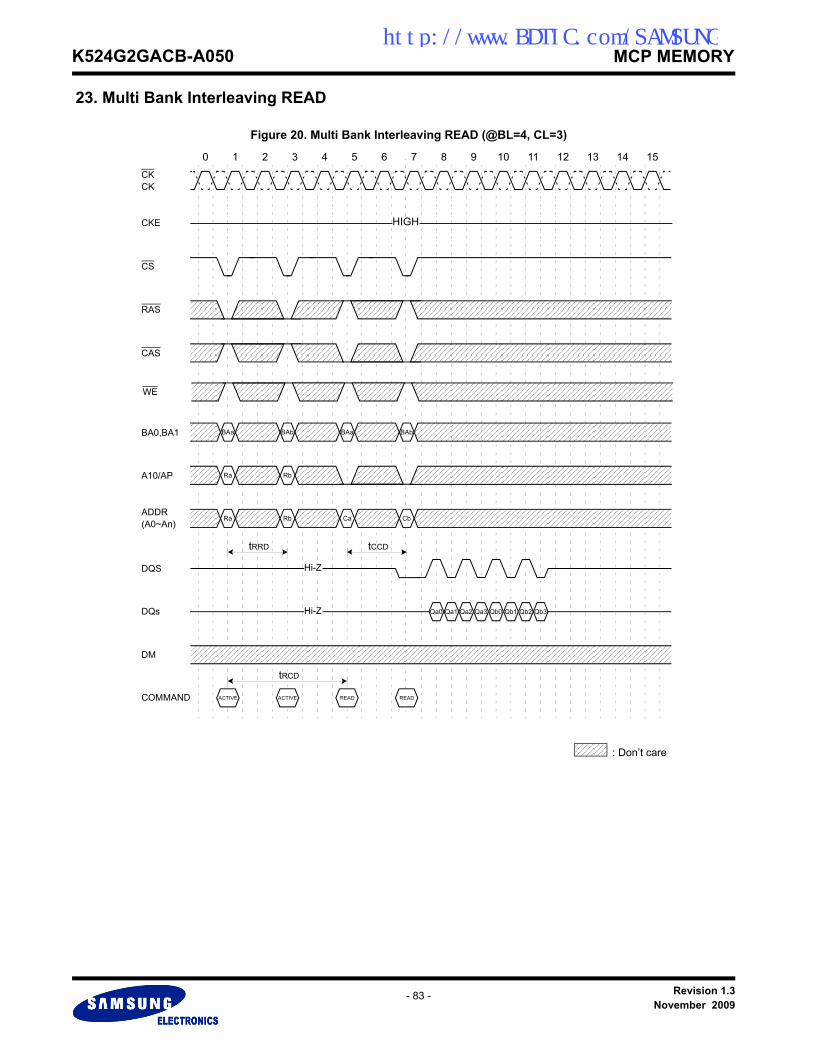
K524G2GACB-A050 MCP MEMORYhttp://www.BDTIC.com/SAMSUNG
23. Multi Bank Interleaving READ
Figure 20. Multi Bank Interleaving READ (@BL=4, CL=3)
0 1 2 3 4 5 6 7 8 9 10 11 12 13 14 15
CKE
CS
RAS
CAS
BA0,BA1
A10/AP
ADDR
DQS
(A0~An)
DQs
: Don’t care
CKCK
HIGH
BAa
DM
COMMAND
Qa0 Qa1 Qa2 Qa3 Qb0 Qb1 Qb2 Qb3
ACTIVE
tRRD tCCD
BAb BAa BAb
Ra
Ra Rb Ca Cb
ACTIVE READ READ
tRCD
Rb
WE
Hi-Z
Hi-Z
Revision 1.3November 2009
- 83 -

K524G2GACB-A050 MCP MEMORYhttp://www.BDTIC.com/SAMSUNG
24. Multi Bank Interleaving WRITE
Figure 21. Multi Bank Interleaving WRITE (@BL=4)
0 1 2 3 4 5 6 7 8 9 10 11 12 13 14 15
CKE
CS
RAS
CAS
BA0,BA1
A10/AP
ADDR
DQS
(A0~An)
DQs
: Don’t care
CKCK
HIGH
BAa
DM
COMMAND
Da0 Da1 Da2 Da3 Db0 Db1 Db2 Db3
ACTIVE
tRRD tCCD
BAb BAa BAb
Ra Rb Ca Cb
ACTIVE WRITE WRITE
tRCD
WE
Ra Rb
Hi-Z
Hi-Z
Revision 1.3November 2009
- 84 -

K524G2GACB-A050 MCP MEMORYhttp://www.BDTIC.com/SAMSUNG
25. Read with Auto Precharge
Figure 22. Read with Auto Precharge (@BL=8)
NOTE :1) The row active command of the precharge bank can be issued after tRP from this point.
0 1 2 3 4 5 6 7 8 9 10
CKE
CS
RAS
CAS
A10/AP
ADDR
DQs
DQS
BA0,BA1
(A0~An)
DM
: Don’t care
CKCK
HIGH
BAa
Qa0 Qa1 Qa2 Qa4 Qa5 Qa6
COMMAND READ
Qa7Qa3
ACTIVE
Ra
Ca Ra
(CL=3)
(CL=3)
Auto precharge starttRP
NOTE1)
WE
BAa
Hi-Z
Hi-Z
Revision 1.3November 2009
- 85 -

K524G2GACB-A050 MCP MEMORYhttp://www.BDTIC.com/SAMSUNG
26. Write with Auto Precharge
Figure 23. Write with Auto Precharge (@BL=8)
NOTE : 1) The row active command of the precharge bank can be issued after tRP from this point
0 1 2 3 4 5 6 7 8 9 10 11 12 13 14 15
Auto precharge start
CKE
CS
RAS
CAS
BA0,BA1
A10/AP
ADDR
DQS
(A0~An)
DQs
: Don’t care
CKCK
HIGH
BAa BAa
Ra
Ca Ra
DM
COMMAND
Da0 Da1 Da2 Da3 Da4 Da5 Da6 Da7
WRITE ACTIVE
NOTE1)tWR tRP
WE
Hi-Z
Hi-Z
Revision 1.3November 2009
- 86 -

K524G2GACB-A050 MCP MEMORYhttp://www.BDTIC.com/SAMSUNG
27. Write followed by Precharge
Figure 24. Write followed by Precharge (@BL=4)
0 1 2 3 4 5 6 7 8 9 10
CKE
CS
RAS
CAS
A10/AP
ADDR
DQs
DQS
BA0,BA1
(A0~An)
DM
: Don’t care
CKCK
HIGH
Da0 Da1 Da2 Da3
COMMAND WRITE
BAa
Ca
PRECHARGE
tWR
BAa
WE
Hi-Z
Hi-Z
Revision 1.3November 2009
- 87 -
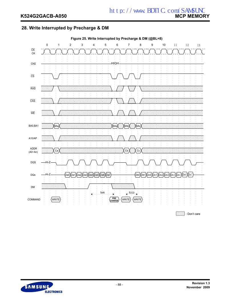
K524G2GACB-A050 MCP MEMORYhttp://www.BDTIC.com/SAMSUNG
28. Write Interrupted by Precharge & DM
Figure 25. Write Interrupted by Precharge & DM (@BL=8)
0 1 2 3 4 5 6 7 8 9 10
CKE
CS
RAS
CAS
A10/AP
ADDR
DQs
DQS
BA0,BA1
(A0~An)
DM
: Don’t care
CKCK
HIGH
BAa
Da0 Da1 Da2 Da3 Da4 Da6 Da7
COMMAND WRITE
Da5
tWR
BAb BAcBAa
Ca Cb Cc
Db0 Db1 Dc0 Dc2 Dc3Dc1
tCCD
PRECHARGE WRITE WRITE
WE
Dc4 Dc5
11 12
Dc6 Dc7
13
Hi-Z
Hi-Z
Revision 1.3November 2009
- 88 -

K524G2GACB-A050 MCP MEMORYhttp://www.BDTIC.com/SAMSUNG
29. Write Interrupted by a Read
Figure 26. Write Interrupted by a Read (@BL=8, CL=3)
0 1 2 3 4 5 6 7 8 9
CKE
CS
RAS
CAS
A10/AP
ADDR
DQs
DQS
BA0,BA1
(A0~An)
DM
: Don’t care
CKCK
HIGH
Da0 Da1 Da2 Da3 Da4 Da5
COMMAND WRITE
BAb
Ca Cb
Qb0 Qb1 Qb2 Qb3
READ
tCDLR
Masked by DM
BAa
WE
Qb4 Qb5 Qb6 Qb7
10 11
Hi-Z
Hi-Z
Revision 1.3November 2009
- 89 -
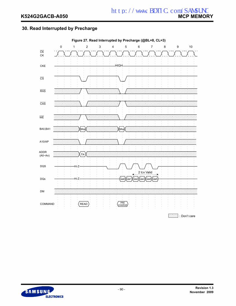
K524G2GACB-A050 MCP MEMORYhttp://www.BDTIC.com/SAMSUNG
30. Read Interrupted by Precharge
Figure 27. Read Interrupted by Precharge (@BL=8, CL=3)
0 1 2 3 4 5 6 7 8 9 10
CKE
CS
RAS
CAS
A10/AP
ADDR
DQs
DQS
BA0,BA1
(A0~An)
DM
: Don’t care
CKCK
HIGH
Qa0 Qa1 Qa2 Qa3 Qa4
COMMAND READ
BAa
Qa5
PRE
BAa
Ca
CHARGE
2 tCK Valid
WE
Hi-Z
Hi-Z
Revision 1.3November 2009
- 90 -

K524G2GACB-A050 MCP MEMORYhttp://www.BDTIC.com/SAMSUNG
31. Read Interrupted by a Write & Burst Stop
Figure 28. Read Interrupted by a Write & Burst Stop (@BL=8, CL=3)
0 1 2 3 4 5 6 7 8 9 10
CKE
CS
RAS
CAS
A10/AP
ADDR
DQs
DQS
BA0,BA1
(A0~An)
DM
: Don’t care
CKCK
HIGH
Qa0 Qa1 Qb0 Qb1 Qb2 Qb4 Qb5 Qb6
COMMAND READ
BAa
Qb7Qb3
Burst
BAb
Ca Cb
WRITEStop
WE
11
Hi-Z
Hi-Z
Revision 1.3November 2009
- 91 -

K524G2GACB-A050 MCP MEMORYhttp://www.BDTIC.com/SAMSUNG
32. Read Interrupted by a Read
Figure 29. Read Interrupted by a Read (@BL=8, CL=3)
0 1 2 3 4 5 6 7 8 9 10
CKE
CS
RAS
CAS
A10/AP
ADDR
DQs
DQS
BA0,BA1
(A0~An)
DM
: Don’t care
CKCK
HIGH
BAa
Qa0 Qa1 Qb0 Qb1 Qb2 Qb4 Qb5 Qb6
COMMAND READ
BAb
Ca Cb
Qb7Qb3
READ
WE
Hi-Z
Hi-Z
Revision 1.3November 2009
- 92 -

K524G2GACB-A050 MCP MEMORYhttp://www.BDTIC.com/SAMSUNG
33. DM Function
Figure 30. DM Function (@BL=8) only for write
0 1 2 3 4 5 6 7 8 9 10
CKE
CS
RAS
CAS
A10/AP
ADDR
DQs
DQS
BA0,BA1
(A0~An)
DM
: Don’t care
CKCK
HIGH
BAa
Ca
Da0 Da1 Da2 Da3 Da5 Da6 Da7
COMMAND WRITE
Da4
WE
Hi-Z
Hi-Z
Revision 1.3November 2009
- 93 -

K524G2GACB-A050 MCP MEMORYhttp://www.BDTIC.com/SAMSUNG
34. Mode Register Set
Figure 31. Mode Register Set
0 1 2 3 4 5 6 7 8 9 10 11 12 13 14 15 16 17
tRP
PrechargeCommandAll Bank
MRSCommand
AnyCommand
CKE
CS
RAS
CAS
BA0,BA1
A10/AP
ADDR
DQs
DM
WE
(A0~An)
DQS
: Don’t care
CKCK
ADDRESS KEY
tMRD
COMMAND
Key
Key
Key
Hi-Z
Hi-Z
HIGH
Revision 1.3November 2009
- 94 -