mcbsp reference guide- spru580c
TRANSCRIPT

8/7/2019 McBSP Reference Guide- spru580c
http://slidepdf.com/reader/full/mcbsp-reference-guide-spru580c 1/120
TMS320C6000 DSP Multichannel Buffered Serial Port (McBSP)
Reference Guide
Literature Number: SPRU580CMarch 2004

8/7/2019 McBSP Reference Guide- spru580c
http://slidepdf.com/reader/full/mcbsp-reference-guide-spru580c 2/120
IMPORTANT NOTICE
Texas Instruments Incorporated and its subsidiaries (TI) reserve the right to make corrections, modifications,
enhancements, improvements, and other changes to its products and services at any time and to discontinue
any product or service without notice. Customers should obtain the latest relevant information before placing
orders and should verify that such information is current and complete. All products are sold subject to TI’s terms
and conditions of sale supplied at the time of order acknowledgment.
TI warrants performance of its hardware products to the specifications applicable at the time of sale in
accordance with TI’s standard warranty. Testing and other quality control techniques are used to the extent TI
deems necessary to support this warranty. Except where mandated by government requirements, testing of all
parameters of each product is not necessarily performed.
TI assumes no liability for applications assistance or customer product design. Customers are responsible for
their products and applications using TI components. To minimize the risks associated with customer products
and applications, customers should provide adequate design and operating safeguards.
TI does not warrant or represent that any license, either express or implied, is granted under any TI patent right,
copyright, mask work right, or other TI intellectual property right relating to any combination, machine, or process
in which TI products or services are used. Information published by TI regarding third-party products or services
does not constitute a license from TI to use such products or services or a warranty or endorsement thereof.Use of such information may require a license from a third party under the patents or other intellectual property
of the third party, or a license from TI under the patents or other intellectual property of TI.
Reproduction of information in TI data books or data sheets is permissible only if reproduction is without
alteration and is accompanied by all associated warranties, conditions, limitations, and notices. Reproduction
of this information with alteration is an unfair and deceptive business practice. TI is not responsible or liable for
such altered documentation.
Resale of TI products or services with statements different from or beyond the parameters stated by TI for that
product or service voids all express and any implied warranties for the associated TI product or service and
is an unfair and deceptive business practice. TI is not responsible or liable for any such statements.
Following are URLs where you can obtain information on other Texas Instruments products and application
solutions:
Products Applications
Amplifiers amplifier.ti.com Audio www.ti.com/audio
Data Converters dataconverter.ti.com Automotive www.ti.com/automotive
DSP dsp.ti.com Broadband www.ti.com/broadband
Interface interface.ti.com Digital Control www.ti.com/digitalcontrol
Logic logic.ti.com Military www.ti.com/military
Power Mgmt power.ti.com Optical Networking www.ti.com/opticalnetwork
Microcontrollers microcontroller.ti.com Security www.ti.com/security
Telephony www.ti.com/telephony
Video & Imaging www.ti.com/video
Wireless www.ti.com/wireless
Mailing Address: Texas Instruments
Post Office Box 655303 Dallas, Texas 75265
Copyright 2004, Texas Instruments Incorporated
8/7/2019 McBSP Reference Guide- spru580c
http://slidepdf.com/reader/full/mcbsp-reference-guide-spru580c 3/120
3Multichannel Buffered Serial Port (McBSP)SPRU580C
Preface
Read This First
About This Manual
This document describes the operation of the multichannel buffered serial port
(McBSP) in the digital signal processors (DSPs) of the TMS320C6000 DSP
family.
Notational Conventions
This document uses the following conventions.
- Hexadecimal numbers are shown with the suffix h. For example, the
following number is 40 hexadecimal (decimal 64): 40h.
- Registers in this document are shown in figures and described in tables.
J Each register figure shows a rectangle divided into fields that represent
the fields of the register. Each field is labeled with its bit name, its
beginning and ending bit numbers above, and its read/write properties
below. A legend explains the notation used for the properties.
J Reserved bits in a register figure designate a bit that is used for futuredevice expansion.
Related Documentation From Texas Instruments
The following documents describe the C6000 devices and related support
tools. Copies of these documents are available on the Internet at www.ti.com.
Tip: Enter the literature number in the search box provided at www.ti.com.
TMS320C6000 CPU and Instruction Set Reference Guide (literature
number SPRU189) describes the TMS320C6000 CPU architecture,
instruction set, pipeline, and interrupts for these digital signal processors.
TMS320C6000 DSP Peripherals Overview Reference Guide (literature
number SPRU190) describes the peripherals available on the
TMS320C6000 DSPs.
TMS320C6000 Technical Brief (literature number SPRU197) gives an
introduction to the TMS320C62x and TMS320C67x DSPs, develop-
ment tools, and third-party support.
8/7/2019 McBSP Reference Guide- spru580c
http://slidepdf.com/reader/full/mcbsp-reference-guide-spru580c 4/120
Trademarks
4 Multichannel Buffered Serial Port (McBSP) SPRU580C
TMS320C64x Technical Overview (SPRU395) gives an introduction to the
TMS320C64x DSP and discusses the application areas that are
enhanced by the TMS320C64x VelociTI.
TMS320C6000 Programmer’s Guide (literature number SPRU198)
describes ways to optimize C and assembly code for the
TMS320C6000 DSPs and includes application program examples.
TMS320C6000 Code Composer Studio Tutorial (literature number
SPRU301) introduces the Code Composer Studio integrated develop-
ment environment and software tools.
Code Composer Studio Application Programming Interface Reference
Guide (literature number SPRU321) describes the Code Composer
Studio application programming interface (API), which allows you to
program custom plug-ins for Code Composer.
TMS320C6x Peripheral Support Library Programmer’s Reference
(literature number SPRU273) describes the contents of the
TMS320C6000 peripheral support library of functions and macros. It
lists functions and macros both by header file and alphabetically,
provides a complete description of each, and gives code examples to
show how they are used.
TMS320C6000 Chip Support Library API Reference Guide (literature
number SPRU401) describes a set of application programming interfaces
(APIs) used to configure and control the on-chip peripherals.
Trademarks
Code Composer Studio, C6000, C62x, C64x, C67x, TMS320C6000,
TMS320C62x, TMS320C64x, TMS320C67x, and VelociTI are trademarks of
Texas Instruments.
SPI is a trademark of Motorola, Inc.
ST-BUS is a trademark of Mitel Networks Corporation.
Related Documentation From Texas Instruments / Trademarks
8/7/2019 McBSP Reference Guide- spru580c
http://slidepdf.com/reader/full/mcbsp-reference-guide-spru580c 5/120
Contents
5Multichannel Buffered Serial Port (McBSP)SPRU580C
Contents
1 Features 11. . . . . . . . . . . . . . . . . . . . . . . . . . . . . . . . . . . . . . . . . . . . . . . . . . . . . . . . . . . . . . . . . . . . . . . . .
2 McBSP Interface 13. . . . . . . . . . . . . . . . . . . . . . . . . . . . . . . . . . . . . . . . . . . . . . . . . . . . . . . . . . . . . . . . . .
3 McBSP Overview 15. . . . . . . . . . . . . . . . . . . . . . . . . . . . . . . . . . . . . . . . . . . . . . . . . . . . . . . . . . . . . . . . .
3.1 Resetting the Serial Port: RRST, XRST, GRST, and RESET 15. . . . . . . . . . . . . . . . . . . . . . .
3.2 Determining Ready Status 17. . . . . . . . . . . . . . . . . . . . . . . . . . . . . . . . . . . . . . . . . . . . . . . . . . . .
3.2.1 Receive Ready Status: REVT, RINT, and RRDY 17. . . . . . . . . . . . . . . . . . . . . . . . . .
3.2.2 Transmit Ready Status: XEVT, XINT, and XRDY 17. . . . . . . . . . . . . . . . . . . . . . . . . .
3.3 CPU Interrupts: RINT, XINT 18. . . . . . . . . . . . . . . . . . . . . . . . . . . . . . . . . . . . . . . . . . . . . . . . . . .
3.4 Frame and Clock Configuration 18. . . . . . . . . . . . . . . . . . . . . . . . . . . . . . . . . . . . . . . . . . . . . . . .
4 Clocks, Frames, and Data 19. . . . . . . . . . . . . . . . . . . . . . . . . . . . . . . . . . . . . . . . . . . . . . . . . . . . . . . . .
4.1 Frame and Clock Operation 20. . . . . . . . . . . . . . . . . . . . . . . . . . . . . . . . . . . . . . . . . . . . . . . . . . .
4.2 Sample Rate Generator Clocking and Framing 22. . . . . . . . . . . . . . . . . . . . . . . . . . . . . . . . . .
4.3 Data Clock Generation 23. . . . . . . . . . . . . . . . . . . . . . . . . . . . . . . . . . . . . . . . . . . . . . . . . . . . . . .
4.3.1 Input Clock Source Mode: CLKSM 23. . . . . . . . . . . . . . . . . . . . . . . . . . . . . . . . . . . . . .
4.3.2 Sample Rate Generator Data Bit Clock Rate: CLKGDV 23. . . . . . . . . . . . . . . . . . . .
4.3.3 Bit Clock Polarity: CLKSP 24. . . . . . . . . . . . . . . . . . . . . . . . . . . . . . . . . . . . . . . . . . . . .
4.3.4 Bit Clock and Frame Synchronization 25. . . . . . . . . . . . . . . . . . . . . . . . . . . . . . . . . . .4.3.5 Digital Loopback Mode: DLB 26. . . . . . . . . . . . . . . . . . . . . . . . . . . . . . . . . . . . . . . . . . .
4.3.6 Receive Clock Selection: DLB, CLKRM 27. . . . . . . . . . . . . . . . . . . . . . . . . . . . . . . . . .
4.3.7 Transmit Clock Selection: CLKXM 27. . . . . . . . . . . . . . . . . . . . . . . . . . . . . . . . . . . . . .
4.3.8 Stopping Clocks 28. . . . . . . . . . . . . . . . . . . . . . . . . . . . . . . . . . . . . . . . . . . . . . . . . . . . . .
4.4 Frame Sync Generation 28. . . . . . . . . . . . . . . . . . . . . . . . . . . . . . . . . . . . . . . . . . . . . . . . . . . . . .
4.4.1 Frame Period (FPER) and Frame Width (FWID) 29. . . . . . . . . . . . . . . . . . . . . . . . . .
4.4.2 Receive Frame Sync Selection: DLB, FSRM, GSYNC 30. . . . . . . . . . . . . . . . . . . . .
4.4.3 Transmit Frame Sync Selection: FSXM, FSGM 31. . . . . . . . . . . . . . . . . . . . . . . . . . .
4.4.4 Frame Detection for Initialization 31. . . . . . . . . . . . . . . . . . . . . . . . . . . . . . . . . . . . . . .
4.5 Data and Frames 32. . . . . . . . . . . . . . . . . . . . . . . . . . . . . . . . . . . . . . . . . . . . . . . . . . . . . . . . . . . .
4.5.1 Frame Synchronization Phases 32. . . . . . . . . . . . . . . . . . . . . . . . . . . . . . . . . . . . . . . .
4.5.2 Frame Length: RFRLEN1/2, XFRLEN1/2 33. . . . . . . . . . . . . . . . . . . . . . . . . . . . . . . .4.5.3 Element Length: RWDLEN1/2, XWDLEN1/2 34. . . . . . . . . . . . . . . . . . . . . . . . . . . . .
4.5.4 Data Packing using Frame Length and Element Length 34. . . . . . . . . . . . . . . . . . .
4.5.5 Data Delay: RDATDLY, XDATDLY 36. . . . . . . . . . . . . . . . . . . . . . . . . . . . . . . . . . . . . .
4.5.6 Receive Data Justification and Sign Extension: RJUST 37. . . . . . . . . . . . . . . . . . . .
4.5.7 32-Bit Bit Reversal: RWDREVRS, XWDREVRS 38. . . . . . . . . . . . . . . . . . . . . . . . . .
8/7/2019 McBSP Reference Guide- spru580c
http://slidepdf.com/reader/full/mcbsp-reference-guide-spru580c 6/120
Contents
6 Multichannel Buffered Serial Port (McBSP) SPRU580C
4.6 Clocking and Framing Examples 38. . . . . . . . . . . . . . . . . . . . . . . . . . . . . . . . . . . . . . . . . . . . . . .
4.6.1 Multiphase Frame Example: AC97 38. . . . . . . . . . . . . . . . . . . . . . . . . . . . . . . . . . . . . .
4.6.2 Double-Rate ST-BUS Clock 40. . . . . . . . . . . . . . . . . . . . . . . . . . . . . . . . . . . . . . . . . . . .4.6.3 Single-Rate ST-BUS Clock 41. . . . . . . . . . . . . . . . . . . . . . . . . . . . . . . . . . . . . . . . . . . .
4.6.4 Double-Rate Clock 42. . . . . . . . . . . . . . . . . . . . . . . . . . . . . . . . . . . . . . . . . . . . . . . . . . .
5 McBSP Standard Operation 43. . . . . . . . . . . . . . . . . . . . . . . . . . . . . . . . . . . . . . . . . . . . . . . . . . . . . . .
5.1 Receive Operation 44. . . . . . . . . . . . . . . . . . . . . . . . . . . . . . . . . . . . . . . . . . . . . . . . . . . . . . . . . . .
5.2 Transmit Operation 45. . . . . . . . . . . . . . . . . . . . . . . . . . . . . . . . . . . . . . . . . . . . . . . . . . . . . . . . . .
5.3 Maximum Frame Frequency 46. . . . . . . . . . . . . . . . . . . . . . . . . . . . . . . . . . . . . . . . . . . . . . . . . .
5.4 Frame Synchronization Ignore 47. . . . . . . . . . . . . . . . . . . . . . . . . . . . . . . . . . . . . . . . . . . . . . . . .
5.4.1 Frame Sync Ignore and Unexpected Frame Sync Pulses 47. . . . . . . . . . . . . . . . . .
5.4.2 Data Packing using Frame Sync Ignore Bits 49. . . . . . . . . . . . . . . . . . . . . . . . . . . . .
5.5 Serial Port Exception Conditions 50. . . . . . . . . . . . . . . . . . . . . . . . . . . . . . . . . . . . . . . . . . . . . . .
5.5.1 Receive Overrun: RFULL 50. . . . . . . . . . . . . . . . . . . . . . . . . . . . . . . . . . . . . . . . . . . . . .5.5.2 Unexpected Receive Frame Synchronization: RSYNCERR 52. . . . . . . . . . . . . . . .
5.5.3 Transmit With Data Overwrite 54. . . . . . . . . . . . . . . . . . . . . . . . . . . . . . . . . . . . . . . . . .
5.5.4 Transmit Empty: XEMPTY 55. . . . . . . . . . . . . . . . . . . . . . . . . . . . . . . . . . . . . . . . . . . . .
5.5.5 Unexpected Transmit Frame Synchronization: XSYNCERR 56. . . . . . . . . . . . . . . .
6 m-Law/A-Law Companding Hardware Operation 59. . . . . . . . . . . . . . . . . . . . . . . . . . . . . . . . . . . . .
6.1 Companding Internal Data 60. . . . . . . . . . . . . . . . . . . . . . . . . . . . . . . . . . . . . . . . . . . . . . . . . . . .
6.2 Bit Ordering 61. . . . . . . . . . . . . . . . . . . . . . . . . . . . . . . . . . . . . . . . . . . . . . . . . . . . . . . . . . . . . . . . .
7 McBSP Initialization Procedure 62. . . . . . . . . . . . . . . . . . . . . . . . . . . . . . . . . . . . . . . . . . . . . . . . . . . .
7.1 General Initialization Procedure 63. . . . . . . . . . . . . . . . . . . . . . . . . . . . . . . . . . . . . . . . . . . . . . .
7.2 Special Case: External Device is the Transmit Frame Master 65. . . . . . . . . . . . . . . . . . . . . .
8 Multichannel Selection Operation 68. . . . . . . . . . . . . . . . . . . . . . . . . . . . . . . . . . . . . . . . . . . . . . . . . .
8.1 Enabling Multichannel Selection 69. . . . . . . . . . . . . . . . . . . . . . . . . . . . . . . . . . . . . . . . . . . . . . .
8.2 Enabling and Masking of Channels in Normal Multichannel Selection Mode 69. . . . . . . . .
8.2.1 Changing Element Selection 73. . . . . . . . . . . . . . . . . . . . . . . . . . . . . . . . . . . . . . . . . . .
8.2.2 End-of-Subframe Interrupt 73. . . . . . . . . . . . . . . . . . . . . . . . . . . . . . . . . . . . . . . . . . . . .
8.3 Enhanced Multichannel Selection Mode (C64x DSP only) 73. . . . . . . . . . . . . . . . . . . . . . . . .
8.4 DX Enabler: DXENA 75. . . . . . . . . . . . . . . . . . . . . . . . . . . . . . . . . . . . . . . . . . . . . . . . . . . . . . . . .
9 SPI Protocol: CLKSTP 77. . . . . . . . . . . . . . . . . . . . . . . . . . . . . . . . . . . . . . . . . . . . . . . . . . . . . . . . . . . .
9.1 McBSP Operation as the SPI Master 80. . . . . . . . . . . . . . . . . . . . . . . . . . . . . . . . . . . . . . . . . . .
9.2 McBSP Operation as the SPI Slave 81. . . . . . . . . . . . . . . . . . . . . . . . . . . . . . . . . . . . . . . . . . . .
9.3 McBSP Initialization for SPI Mode 81. . . . . . . . . . . . . . . . . . . . . . . . . . . . . . . . . . . . . . . . . . . . .
10 McBSP Pins as General-Purpose I/O 83. . . . . . . . . . . . . . . . . . . . . . . . . . . . . . . . . . . . . . . . . . . . . . .

8/7/2019 McBSP Reference Guide- spru580c
http://slidepdf.com/reader/full/mcbsp-reference-guide-spru580c 7/120
Contents
7Multichannel Buffered Serial Port (McBSP)SPRU580C
11 Registers 84. . . . . . . . . . . . . . . . . . . . . . . . . . . . . . . . . . . . . . . . . . . . . . . . . . . . . . . . . . . . . . . . . . . . . . . .
11.1 Data Receive Register (DRR) 87. . . . . . . . . . . . . . . . . . . . . . . . . . . . . . . . . . . . . . . . . . . . . . . . .
11.2 Data Transmit Register (DXR) 88. . . . . . . . . . . . . . . . . . . . . . . . . . . . . . . . . . . . . . . . . . . . . . . . .11.3 Serial Port Control Register (SPCR) 89. . . . . . . . . . . . . . . . . . . . . . . . . . . . . . . . . . . . . . . . . . . .
11.4 Receive Control Register (RCR) 94. . . . . . . . . . . . . . . . . . . . . . . . . . . . . . . . . . . . . . . . . . . . . . .
11.5 Transmit Control Register (XCR) 97. . . . . . . . . . . . . . . . . . . . . . . . . . . . . . . . . . . . . . . . . . . . . . .
11.6 Sample Rate Generator Register (SRGR) 99. . . . . . . . . . . . . . . . . . . . . . . . . . . . . . . . . . . . . . .
11.7 Multichannel Control Register (MCR) 101. . . . . . . . . . . . . . . . . . . . . . . . . . . . . . . . . . . . . . . . . .
11.8 Receive Channel Enable Register (RCER) 105. . . . . . . . . . . . . . . . . . . . . . . . . . . . . . . . . . . . .
11.9 Transmit Channel Enable Registers (XCER) 106. . . . . . . . . . . . . . . . . . . . . . . . . . . . . . . . . . .
11.10 Enhanced Receive Channel Enable Registers (RCERE0−3) 107. . . . . . . . . . . . . . . . . . . . . .
11.11 Enhanced Transmit Channel Enable Registers (XCERE0−3) 109. . . . . . . . . . . . . . . . . . . . .
11.12 Pin Control Register (PCR) 111. . . . . . . . . . . . . . . . . . . . . . . . . . . . . . . . . . . . . . . . . . . . . . . . . .
Revision History 115. . . . . . . . . . . . . . . . . . . . . . . . . . . . . . . . . . . . . . . . . . . . . . . . . . . . . . . . . . . . . . . . . . . .

8/7/2019 McBSP Reference Guide- spru580c
http://slidepdf.com/reader/full/mcbsp-reference-guide-spru580c 8/120
Figures
8 Multichannel Buffered Serial Port (McBSP) SPRU580C
Figures
1 McBSP Block Diagram 13. . . . . . . . . . . . . . . . . . . . . . . . . . . . . . . . . . . . . . . . . . . . . . . . . . . . . . . . . .
2 Frame and Clock Operation 19. . . . . . . . . . . . . . . . . . . . . . . . . . . . . . . . . . . . . . . . . . . . . . . . . . . . .
3 Clock and Frame Generation 19. . . . . . . . . . . . . . . . . . . . . . . . . . . . . . . . . . . . . . . . . . . . . . . . . . . .
4 Receive Data Clocking 21. . . . . . . . . . . . . . . . . . . . . . . . . . . . . . . . . . . . . . . . . . . . . . . . . . . . . . . . . .
5 Transmit Data Clocking 21. . . . . . . . . . . . . . . . . . . . . . . . . . . . . . . . . . . . . . . . . . . . . . . . . . . . . . . . .
6 Sample Rate Generator 22. . . . . . . . . . . . . . . . . . . . . . . . . . . . . . . . . . . . . . . . . . . . . . . . . . . . . . . . .7 CLKG Synchronization and FSG Generation When GSYNC = 1 and CLKGDV = 1 25. . . . . .
8 CLKG Synchronization and FSG Generation When GSYNC = 1 and CLKGDV = 3 26. . . . . .
9 Programmable Frame Period and Width 29. . . . . . . . . . . . . . . . . . . . . . . . . . . . . . . . . . . . . . . . . .
10 Dual-Phase Frame Example 32. . . . . . . . . . . . . . . . . . . . . . . . . . . . . . . . . . . . . . . . . . . . . . . . . . . . .
11 Single-Phase Frame of Four 8-Bit Elements 35. . . . . . . . . . . . . . . . . . . . . . . . . . . . . . . . . . . . . . .
12 Single-Phase Frame of One 32-Bit Element 35. . . . . . . . . . . . . . . . . . . . . . . . . . . . . . . . . . . . . . .
13 Data Delay 36. . . . . . . . . . . . . . . . . . . . . . . . . . . . . . . . . . . . . . . . . . . . . . . . . . . . . . . . . . . . . . . . . . . .
14 2-Bit Data Delay Used to Discard Framing Bit 37. . . . . . . . . . . . . . . . . . . . . . . . . . . . . . . . . . . . . .
15 AC97 Dual-Phase Frame Format 38. . . . . . . . . . . . . . . . . . . . . . . . . . . . . . . . . . . . . . . . . . . . . . . . .
16 AC97 Bit Timing Near Frame Synchronization 39. . . . . . . . . . . . . . . . . . . . . . . . . . . . . . . . . . . . .
17 Double-Rate ST-BUS Clock Example 40. . . . . . . . . . . . . . . . . . . . . . . . . . . . . . . . . . . . . . . . . . . . .
18 Single-Rate ST-BUS Clock Example 41. . . . . . . . . . . . . . . . . . . . . . . . . . . . . . . . . . . . . . . . . . . . . .19 Double-Rate Clock Example 42. . . . . . . . . . . . . . . . . . . . . . . . . . . . . . . . . . . . . . . . . . . . . . . . . . . . .
20 McBSP Standard Operation 43. . . . . . . . . . . . . . . . . . . . . . . . . . . . . . . . . . . . . . . . . . . . . . . . . . . . .
21 Receive Operation 44. . . . . . . . . . . . . . . . . . . . . . . . . . . . . . . . . . . . . . . . . . . . . . . . . . . . . . . . . . . . .
22 Transmit Operation 45. . . . . . . . . . . . . . . . . . . . . . . . . . . . . . . . . . . . . . . . . . . . . . . . . . . . . . . . . . . . .
23 Maximum Frame Frequency for Transmit and Receive 46. . . . . . . . . . . . . . . . . . . . . . . . . . . . . .
24 Unexpected Frame Synchronization With (R/X)FIG = 0 48. . . . . . . . . . . . . . . . . . . . . . . . . . . . .
25 Unexpected Frame Synchronization With (R/X)FIG = 1 48. . . . . . . . . . . . . . . . . . . . . . . . . . . . .
26 Maximum Frame Frequency Operation With 8-Bit Data 49. . . . . . . . . . . . . . . . . . . . . . . . . . . . .
27 Data Packing at Maximum Frame Frequency With (R/X)FIG = 1 50. . . . . . . . . . . . . . . . . . . . . .
28 Serial Port Receive Overrun 51. . . . . . . . . . . . . . . . . . . . . . . . . . . . . . . . . . . . . . . . . . . . . . . . . . . . .
29 Serial Port Receive Overrun Avoided 52. . . . . . . . . . . . . . . . . . . . . . . . . . . . . . . . . . . . . . . . . . . . .
30 Decision Tree Response to Receive Frame Synchronization Pulse 53. . . . . . . . . . . . . . . . . . .31 Unexpected Receive Synchronization Pulse 54. . . . . . . . . . . . . . . . . . . . . . . . . . . . . . . . . . . . . . .
32 Transmit With Data Overwrite 54. . . . . . . . . . . . . . . . . . . . . . . . . . . . . . . . . . . . . . . . . . . . . . . . . . . .
33 Transmit Empty 55. . . . . . . . . . . . . . . . . . . . . . . . . . . . . . . . . . . . . . . . . . . . . . . . . . . . . . . . . . . . . . . .
34 Transmit Empty Avoided 56. . . . . . . . . . . . . . . . . . . . . . . . . . . . . . . . . . . . . . . . . . . . . . . . . . . . . . . .
35 Decision Tree Response to Transmit Frame Synchronization Pulse 58. . . . . . . . . . . . . . . . . . .

8/7/2019 McBSP Reference Guide- spru580c
http://slidepdf.com/reader/full/mcbsp-reference-guide-spru580c 9/120
Figures
9Multichannel Buffered Serial Port (McBSP)SPRU580C
36 Unexpected Transmit Frame Synchronization Pulse 58. . . . . . . . . . . . . . . . . . . . . . . . . . . . . . . .
37 Companding Flow 59. . . . . . . . . . . . . . . . . . . . . . . . . . . . . . . . . . . . . . . . . . . . . . . . . . . . . . . . . . . . . .
38 Companding Data Formats 60. . . . . . . . . . . . . . . . . . . . . . . . . . . . . . . . . . . . . . . . . . . . . . . . . . . . . .39 Transmit Data Companding Format in DXR 60. . . . . . . . . . . . . . . . . . . . . . . . . . . . . . . . . . . . . . . .
40 Companding of Internal Data 61. . . . . . . . . . . . . . . . . . . . . . . . . . . . . . . . . . . . . . . . . . . . . . . . . . . .
41 Element Enabling by Subframes in Partitions A and B 69. . . . . . . . . . . . . . . . . . . . . . . . . . . . . . .
42 XMCM Operation 71. . . . . . . . . . . . . . . . . . . . . . . . . . . . . . . . . . . . . . . . . . . . . . . . . . . . . . . . . . . . . .
43 DX Timing for Multichannel Operation 75. . . . . . . . . . . . . . . . . . . . . . . . . . . . . . . . . . . . . . . . . . . .
44 SPI Configuration: McBSP as the Master 77. . . . . . . . . . . . . . . . . . . . . . . . . . . . . . . . . . . . . . . . . .
45 SPI Configuration: McBSP as the Slave 77. . . . . . . . . . . . . . . . . . . . . . . . . . . . . . . . . . . . . . . . . . .
46 SPI Transfer with CLKSTP = 10b 78. . . . . . . . . . . . . . . . . . . . . . . . . . . . . . . . . . . . . . . . . . . . . . . . .
47 SPI Transfer with CLKSTP = 11b 79. . . . . . . . . . . . . . . . . . . . . . . . . . . . . . . . . . . . . . . . . . . . . . . . .
48 Data Receive Register (DRR) 87. . . . . . . . . . . . . . . . . . . . . . . . . . . . . . . . . . . . . . . . . . . . . . . . . . . .
49 Data Transmit Register (DXR) 88. . . . . . . . . . . . . . . . . . . . . . . . . . . . . . . . . . . . . . . . . . . . . . . . . . .
50 Serial Port Control Register (SPCR) 89. . . . . . . . . . . . . . . . . . . . . . . . . . . . . . . . . . . . . . . . . . . . . .
51 Receive Control Register (RCR) 94. . . . . . . . . . . . . . . . . . . . . . . . . . . . . . . . . . . . . . . . . . . . . . . . .
52 Transmit Control Register (XCR) 97. . . . . . . . . . . . . . . . . . . . . . . . . . . . . . . . . . . . . . . . . . . . . . . . .
53 Sample Rate Generator Register (SRGR) 99. . . . . . . . . . . . . . . . . . . . . . . . . . . . . . . . . . . . . . . . .
54 Multichannel Control Register (MCR) 101. . . . . . . . . . . . . . . . . . . . . . . . . . . . . . . . . . . . . . . . . . . .
55 Receive Channel Enable Register (RCER) 105. . . . . . . . . . . . . . . . . . . . . . . . . . . . . . . . . . . . . . .
56 Transmit Channel Enable Register (XCER) 106. . . . . . . . . . . . . . . . . . . . . . . . . . . . . . . . . . . . . . .
57 Enhanced Receive Channel Enable Registers (RCERE0−3) 107. . . . . . . . . . . . . . . . . . . . . . . .
58 Enhanced Transmit Channel Enable Registers (XCERE0−3) 109. . . . . . . . . . . . . . . . . . . . . . . .
59 Pin Control Register (PCR) 111. . . . . . . . . . . . . . . . . . . . . . . . . . . . . . . . . . . . . . . . . . . . . . . . . . . . .

8/7/2019 McBSP Reference Guide- spru580c
http://slidepdf.com/reader/full/mcbsp-reference-guide-spru580c 10/120
Tables
10 Multichannel Buffered Serial Port (McBSP) SPRU580C
Tables
1 Enhanced Features on TMS320C6000 McBSP 12. . . . . . . . . . . . . . . . . . . . . . . . . . . . . . . . . . . .
2 McBSP Interface Pins 14. . . . . . . . . . . . . . . . . . . . . . . . . . . . . . . . . . . . . . . . . . . . . . . . . . . . . . . . . .
3 Reset State of McBSP Pins 15. . . . . . . . . . . . . . . . . . . . . . . . . . . . . . . . . . . . . . . . . . . . . . . . . . . . .
4 Receive Clock Selection 27. . . . . . . . . . . . . . . . . . . . . . . . . . . . . . . . . . . . . . . . . . . . . . . . . . . . . . . .
5 Transmit Clock Selection 27. . . . . . . . . . . . . . . . . . . . . . . . . . . . . . . . . . . . . . . . . . . . . . . . . . . . . . . .
6 Receive Frame Synchronization Selection 30. . . . . . . . . . . . . . . . . . . . . . . . . . . . . . . . . . . . . . . . .
7 Transmit Frame Synchronization Selection 31. . . . . . . . . . . . . . . . . . . . . . . . . . . . . . . . . . . . . . . .
8 RCR/XCR Fields Controlling Elements per Frame and Bits per Element 33. . . . . . . . . . . . . . .
9 Receive/Transmit Frame Length Configuration 33. . . . . . . . . . . . . . . . . . . . . . . . . . . . . . . . . . . . .
10 Receive/Transmit Element Length Configuration 34. . . . . . . . . . . . . . . . . . . . . . . . . . . . . . . . . . .
11 Effect of RJUST Bit Values With 12-Bit Example Data ABCh 37. . . . . . . . . . . . . . . . . . . . . . . . .
12 Justification of Expanded Data in DRR 60. . . . . . . . . . . . . . . . . . . . . . . . . . . . . . . . . . . . . . . . . . . .
13 Receiver Clock and Frame Configurations 62. . . . . . . . . . . . . . . . . . . . . . . . . . . . . . . . . . . . . . . . .
14 Transmitter Clock and Frame Configurations 63. . . . . . . . . . . . . . . . . . . . . . . . . . . . . . . . . . . . . .
15 SPI-Mode Clock Stop Scheme 78. . . . . . . . . . . . . . . . . . . . . . . . . . . . . . . . . . . . . . . . . . . . . . . . . . .
16 Configuration of Pins as General Purpose I/O 83. . . . . . . . . . . . . . . . . . . . . . . . . . . . . . . . . . . . . .
17 McBSP Registers for C620x/C670x DSP 84. . . . . . . . . . . . . . . . . . . . . . . . . . . . . . . . . . . . . . . . . .18 McBSP Registers for C621x/C671x DSP 85. . . . . . . . . . . . . . . . . . . . . . . . . . . . . . . . . . . . . . . . . .
19 McBSP Registers for C64x DSP 86. . . . . . . . . . . . . . . . . . . . . . . . . . . . . . . . . . . . . . . . . . . . . . . . .
20 Data Receive Register (DRR) Field Descriptions 87. . . . . . . . . . . . . . . . . . . . . . . . . . . . . . . . . . .
21 Data Transmit Register (DXR) Field Descriptions 88. . . . . . . . . . . . . . . . . . . . . . . . . . . . . . . . . . .
22 Serial Port Control Register (SPCR) Field Descriptions 90. . . . . . . . . . . . . . . . . . . . . . . . . . . . .
23 Receive Control Register (RCR) Field Descriptions 94. . . . . . . . . . . . . . . . . . . . . . . . . . . . . . . . .
24 Transmit Control Register (XCR) Field Descriptions 97. . . . . . . . . . . . . . . . . . . . . . . . . . . . . . . .
25 Sample Rate Generator Register (SRGR) Field Descriptions 100. . . . . . . . . . . . . . . . . . . . . . .
26 Multichannel Control Register (MCR) Field Descriptions 101. . . . . . . . . . . . . . . . . . . . . . . . . . . .
27 Receive Channel Enable Register (RCER) Field Descriptions 105. . . . . . . . . . . . . . . . . . . . . . .
28 Transmit Channel Enable Register (XCER) Field Descriptions 106. . . . . . . . . . . . . . . . . . . . . .
29 Enhanced Receive Channel Enable Registers (RCERE0−
3) Field Descriptions 107. . . . . . .30 Channel Enable Bits in RCEREn for a 128-Channel Data Stream 108. . . . . . . . . . . . . . . . . . . .
31 Enhanced Transmit Channel Enable Registers (XCERE0−3) Field Descriptions 109. . . . . . .
32 Channel Enable Bits in XCEREn for a 128-Channel Data Stream 110. . . . . . . . . . . . . . . . . . . .
33 Pin Control Register (PCR) Field Descriptions 111. . . . . . . . . . . . . . . . . . . . . . . . . . . . . . . . . . . .
34 Document Revision History 115. . . . . . . . . . . . . . . . . . . . . . . . . . . . . . . . . . . . . . . . . . . . . . . . . . . . .

8/7/2019 McBSP Reference Guide- spru580c
http://slidepdf.com/reader/full/mcbsp-reference-guide-spru580c 11/120
11Multichannel Buffered Serial Port (McBSP)SPRU580C
Multichannel Buffered Serial Port (McBSP)
This document describes the operation of the multichannel buffered serial port
(McBSP) in the digital signal processors (DSPs) of the TMS320C6000 DSP
family.
1 Features
The McBSP provides these functions:
- Full-duplex communication- Double-buffered data registers, which allow a continuous data stream
- Independent framing and clocking for receive and transmit
- Direct interface to industry-standard codecs, analog interface chips (AICs),
and other serially connected analog-to-digital (A/D) and digital-to-analog
(D/A) devices
- External shift clock or an internal, programmable frequency shift clock for
data transfer
In addition, the McBSP has the following capabilities:
- Direct interface to:
JT1/E1 framers
J MVIP switching compatible and ST-BUS compliant devices including:
H MVIP framers
H H.100 framers
H SCSA framers
J IOM-2 compliant devices
J AC97 compliant devices (The necessary multi phase frame
synchronization capability is provided.)
J IIS compliant devices
J SPI devices
- Multichannel transmit and receive of up to 128 channels
- A wide selection of data sizes, including 8, 12, 16, 20, 24, and 32 bits- µ-Law and A-Law companding
- 8-bit data transfers with the option of LSB or MSB first
- Programmable polarity for both frame synchronization and data clocks
- Highly programmable internal clock and frame generation

8/7/2019 McBSP Reference Guide- spru580c
http://slidepdf.com/reader/full/mcbsp-reference-guide-spru580c 12/120
Features
Multichannel Buffered Serial Port (McBSP)12 SPRU580C
All C6000 devices have the same McBSP. However, the C621x/C671x and
C64x McBSP has additional features and enhancements that are summarized
in Table 1.
Table 1. Enhanced Features on TMS320C6000 McBSP
Features C620x/C670x C621x/C671x McBSP C64x McBSP
DX Enabler (DXENA) No Yes Yes
32-bit data reversal(RWDREVRS/XWDREVRS)
No Yes Yes
Enhanced multichannelselection mode
(RMCME/XMCME)
No No Yes
Emulation control(FREE, SOFT)
No Yes Yes
8/7/2019 McBSP Reference Guide- spru580c
http://slidepdf.com/reader/full/mcbsp-reference-guide-spru580c 13/120
McBSP Interface
13Multichannel Buffered Serial Port (McBSP)SPRU580C
2 McBSP Interface
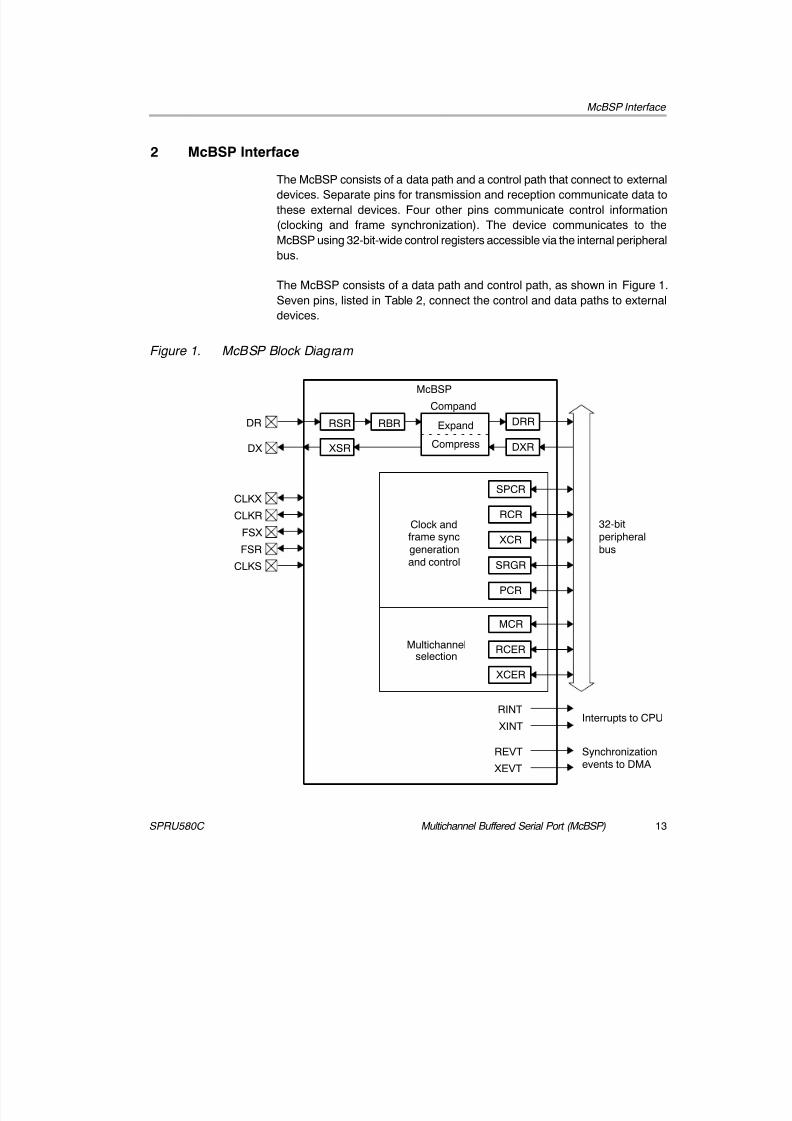
The McBSP consists of a data path and a control path that connect to externaldevices. Separate pins for transmission and reception communicate data to
these external devices. Four other pins communicate control information
(clocking and frame synchronization). The device communicates to the
McBSP using 32-bit-wide control registers accessible via the internal peripheral
bus.
The McBSP consists of a data path and control path, as shown in Figure 1.
Seven pins, listed in Table 2, connect the control and data paths to external
devices.
Figure 1. McBSP Block Diagram
Á Á Á Á Á Á Á Á Á Á Á Á Á Á Á
Á Á Á Á Á Á Á Á Á Á Á Á Á Á Á
Á Á Á Á Á Á Á Á Á Á Á Á Á Á Á
Á Á Á Á Á Á Á Á Á Á Á Á Á Á Á
Á Á Á Á Á Á Á Á Á Á Á Á Á Á Á
Á Á Á Á Á Á Á Á Á Á Á Á Á Á Á
Á Á Á Á Á Á Á Á Á Á Á Á Á Á Á
Á Á Á Á Á Á Á Á Á Á Á Á Á Á Á
Á Á Á Á Á Á Á Á Á Á Á Á Á Á Á
Á Á Á Á Á Á Á Á Á Á Á Á Á Á Á
Á Á Á Á Á Á Á Á Á Á Á Á Á Á Á
Á Á Á Á Á Á Á Á Á Á Á Á Á Á Á
Á Á Á Á Á Á Á Á Á Á Á Á Á Á Á
Á Á Á Á Á Á Á Á Á Á Á Á Á Á Á
Á Á Á Á Á Á Á Á Á Á Á Á Á Á Á
Á Á Á Á Á Á Á Á Á Á Á Á Á Á Á
Á Á Á Á Á Á Á Á Á Á Á Á Á Á Á
Á Á Á Á Á Á Á Á Á Á Á Á Á Á Á
Á Á Á Á Á Á Á Á Á Á Á Á Á Á Á
Á Á Á Á Á Á Á Á Á Á Á Á Á Á Á
Á Á Á Á Á Á Á Á Á Á Á Á Á Á Á
Á Á Á Á Á Á Á Á Á Á Á Á Á Á Á
Á Á Á Á Á Á Á Á Á Á Á Á Á Á Á
Á Á Á Á Á Á Á Á Á Á Á
Á Á Á Á Á Á Á Á Á Á Á
Á Á Á Á Á Á Á Á Á Á Á
Á Á Á Á Á Á Á Á Á Á Á
Á Á Á Á Á Á Á Á Á Á Á
Á Á Á Á Á Á Á Á Á Á Á
Á Á Á Á Á Á Á Á Á Á Á
Á Á Á Á Á Á Á Á Á Á Á
Á Á Á Á Á Á Á Á Á Á Á
Á Á Á Á Á Á Á Á Á Á Á
Á Á Á Á Á Á Á Á Á Á Á
Á Á Á Á Á Á Á Á Á Á Á
Á Á Á Á Á Á Á Á Á Á Á
Á Á Á Á Á Á Á Á Á Á Á
Á Á Á
Á Á Á
Á Á Á
Á Á Á
Á Á Á
Á Á Á
Á Á Á
Á Á Á
Á Á Á
Á Á Á
SRGR
Á Á Á
Á Á Á
Á Á Á
Á Á Á
Á Á Á
Á Á Á
Á Á
Á Á
Á Á
Á Á Á Á Á
Á Á Á
Á Á Á
Á Á Á
RBRÁ Á Á
Á Á Á
Á Á Á Á Á
Á Á Á Á Á
Á Á Á Á Á
CLKS
FSRFSX
CLKR
CLKX
DX
DR
XEVT
REVT
XINTRINT
events to DMASynchronization
Interrupts to CPU
busperipheral
32-bit
McBSP
Compand
XSR
RSR
Compress
Expand DRR
DXR
Multichannelselection
and controlgenerationframe sync
Clock and
PCR
XCER
RCER
MCR
XCR
SPCR
RCR
8/7/2019 McBSP Reference Guide- spru580c
http://slidepdf.com/reader/full/mcbsp-reference-guide-spru580c 14/120
McBSP Interface
Multichannel Buffered Serial Port (McBSP)14 SPRU580C
Data is communicated to devices interfacing to the McBSP via the data transmit
(DX) pin for transmission and via the data receive (DR) pin for reception. Control
information (clocking and frame synchronization) is communicated via CLKS,CLKX, CLKR, FSX, and FSR. The C6000 CPU communicates to the McBSP
using 32-bit-wide control registers accessible via the internal peripheral bus.
Non-32-bit write accesses to control registers can result in corrupting the control
register value. This is because undefined values are written to non-enabled
bytes. However, non-32-bit read accesses return the correct value.
Either the CPU or the DMA/EDMA controller reads the received data from the
data receive register (DRR) and writes the data to be transmitted to the data
transmit register (DXR). Data written to DXR is shifted out to DX via the transmit
shift register (XSR). Similarly, receive data on the DR pin is shifted into the
receive shift register (RSR) and copied into the receive buffer register (RBR).
RBR is then copied to DRR, which can be read by the CPU or the DMA/EDMAcontroller. This allows simultaneous internal data movement and external data
communications. For information on registers, see section 11.
Table 2. McBSP Interface Pins
Pin I/O/Z Description
CLKR I/O/Z Receive clock
CLKX I/O/Z Transmit clock
CLKS I External clock
DR I Received serial data
DX O/Z Transmitted serial data
FSR I/O/Z Receive frame synchronization
FSX I/O/Z Transmit frame synchronization
8/7/2019 McBSP Reference Guide- spru580c
http://slidepdf.com/reader/full/mcbsp-reference-guide-spru580c 15/120
McBSP Overview
15Multichannel Buffered Serial Port (McBSP)SPRU580C
3 McBSP Overview
As shown in Figure 1, the receive operation is triple-buffered and the transmit
operation is double-buffered. Receive data arrives on the DR and is shifted into
the RSR. Once a full element (8, 12, 16, 20, 24, or 32 bits) is received, the RSR
is copied to the receive buffer register (RBR) only if the RBR is not full. The
RBR is then copied to DRR unless the DRR has not been read by the CPU or
the DMA/EDMA controller.
The CPU or the DMA/EDMA controller writes transmit data to DXR. If there is
no data in XSR, the value in DXR is copied to XSR. Otherwise, the DXR is
copied to XSR when the last bit of data is shifted out on the DX. After transmit
frame synchronization, XSR begins shifting out the transmit data on the DX.
3.1 Resetting the Serial Port: RRST, XRST, GRST, and RESET
The serial port can be reset in the following two ways:
- Device reset (RESET pin is low) places the receiver, the transmitter, and
the sample rate generator in reset. When the device reset is removed
(RESET = 1), FRST = GRST = RRST = XRST = 0, keeping the entire
serial port in the reset state.
- The serial port transmitter and receiver can be independently reset by the
XRST and RRST bits in the serial port control register (SPCR). The sample
rate generator is reset by the GRST bit in SPCR.
Table 3 shows the state of the McBSP pins when the serial port is reset by
these methods.
Table 3. Reset State of McBSP Pins
Pin Direction
Device Reset
(RESET = 0) McBSP Reset
Receiver Reset (RRST = 0 and GRST = 1)
DR I Input Input
CLKR I/O/Z Input Known state if input; CLKR if output
FSR I/O/Z Input Known state if input; FSRP(inactive state) if output
CLKS I Input Input
Transmitter Reset (XRST = 0 and GRST = 1)
DX O/Z High impedance High impedance
CLKX I/O/Z Input Known state if input; CLKX if output
FSX I/O/Z Input Known state if input; FSXP(inactive state) if output
CLKS I Input Input
8/7/2019 McBSP Reference Guide- spru580c
http://slidepdf.com/reader/full/mcbsp-reference-guide-spru580c 16/120
McBSP Overview
Multichannel Buffered Serial Port (McBSP)16 SPRU580C
- Device reset or McBSP reset: When the McBSP is reset by device reset
or McBSP reset, the state machine is reset to its initial state. All counters
and status bits are reset. This includes the receive status bits RFULL,RRDY, and RSYNCERR, and the transmit status bits XEMPTY, XRDY,
and XSYNCERR.
- Device reset: When the McBSP is reset due to device reset, the entire
serial port (including the transmitter, receiver, and the sample rate generator)
is reset. All input-only pins and 3-state pins should be in a known state. The
output-only pin, DX, is in the high-impedance state. See section 4.2 for
more information on the sample rate generator and its default at reset.
When the device is pulled out of reset, the serial port remains in the reset
condition (RRST = XRST = FRST = GRST = 0). In this reset condition,
the serial port pins can be used as general-purpose I/O (see section 10).
- McBSP reset: When the receiver and transmitter reset bits, RRST andXRST, are written with 0, the respective portions of the McBSP are reset
and activity in the corresponding section stops. All input-only pins, such
as DR and CLKS, and all other pins that are configured as inputs are in
a known state. FS(R/X) is driven to its inactive state (same as its polarity
bit, FS(R/X)P) if it is an output. If CLK(R/X) are programmed as outputs,
they are driven by CLKG, provided that GRST = 1. The DX pin is in the
high-impedance state when the transmitter is reset. During normal
operation, the sample rate generator can be reset by writing a 0 to GRST.
GRST should be low only when neither the transmitter nor the receiver is
using the sample rate generator. In this case, the internal sample rate
generator clock CLKG, and its frame sync signal (FSG) is driven inactive
(low). When the sample rate generator is not in the reset state (GRST = 1),FSR and FSX are in an inactive state when RRST = 0 and XRST = 0,
respectively, even if they are outputs driven by FSG. This ensures that
when only one portion of the McBSP is in reset, the other portion can
continue operation when FRST = 1 and frame sync is driven by FSG.
- Sample-rate generator reset: As mentioned previously, the sample rate
generator is reset when the device is reset or when its reset bit, GRST, is
written with 0. See section 5.5.5 to avoid this error.
A transmit frame sync error (XSYNCERR) may occur the first time the
transmitter is enabled (XRST = 1) after a device reset. See section 7 for details
on the McBSP initialization procedure.

8/7/2019 McBSP Reference Guide- spru580c
http://slidepdf.com/reader/full/mcbsp-reference-guide-spru580c 17/120
McBSP Overview
17Multichannel Buffered Serial Port (McBSP)SPRU580C
3.2 Determining Ready Status
The RRDY and XRDY bits in SPCR indicate the ready state of the McBSPreceiver and transmitter, respectively. Writes and reads from the serial port can
be synchronized by any of the following methods:
- Polling RRDY and XRDY bits
- Using the events sent to the DMA or EDMA controller (REVT and XEVT)
- Using the interrupts to the CPU (RINT and XINT) that the events generate
Reading DRR and writing to DXR affects RRDY and XRDY, respectively.
3.2.1 Receive Ready Status: REVT, RINT, and RRDY
RRDY = 1 indicates that the RBR contents have been copied to DRR and that
the data can now be read by either the CPU or the DMA/EDMA controller.Once that data has been read by either the CPU or the DMA/EDMA controller,
RRDY is cleared to 0. Also, at device reset or serial port receiver reset
(RRST = 0), the RRDY bit is cleared to 0 to indicate that no data has been
received and loaded into DRR. RRDY directly drives the McBSP receive event
to the DMA/EDMA controller (via REVT). Also, the McBSP receive interrupt
(RINT) to the CPU can be driven by RRDY, if RINTM = 00b (default value) in
SPCR.
3.2.2 Transmit Ready Status: XEVT, XINT, and XRDY
XRDY = 1 indicates that the DXR contents have been copied to XSR and that
DXR is ready to be loaded with a new data word. When the transmittertransitions from reset to non-reset (XRST transitions from 0 to 1), XRDY also
transitions from 0 to 1 indicating that DXR is ready for new data. Once new data
is loaded by the CPU or the DMA/EDMA controller, the XRDY bit is cleared to
0. However, once this data is copied from DXR to XSR, the XRDY bit
transitions again from 0 to 1. The CPU or the DMA/EDMA controller can write
to DXR although XSR has not yet been shifted out on DX. XRDY directly drives
the transmit synchronization event to the DMA/EDMA controller (via XEVT).
Also, the McBSP transmit interrupt (XINT) to the CPU can be driven by XRDY,
if XINTM = 00b (default value) in SPCR.
Note:
If the polling method is used to service the transmitter, the CPU should waitfor one McBSP bit clock (CLKX) before polling again to write the next elementin DXR. This is because XRDY transitions occur based on bit clock and notCPU clock. The CPU clock is much faster and can cause false XRDY status,leading to data errors due to over-writes.

8/7/2019 McBSP Reference Guide- spru580c
http://slidepdf.com/reader/full/mcbsp-reference-guide-spru580c 18/120
McBSP Overview
Multichannel Buffered Serial Port (McBSP)18 SPRU580C
3.3 CPU Interrupts: RINT, XINT
The receive interrupt (RINT) and transmit interrupt (XINT) signals inform theCPU of changes to the serial port status. Four options exist for configuring
these interrupts. These options are set by the receive/transmit interrupt mode
bits (RINTM and XINTM) in SPCR. The possible values of the mode, and the
configurations they represent, are:
- (R/X)INTM = 00b. Interrupt on every serial element by tracking the
(R/X)RDY bits in SPCR.
- (R/X)INTM = 01b. Interrupt at the end of a subframe (16 elements or less)
within a frame. See section 8.2.2 for details.
- (R/X)INTM = 10b. Interrupt on detection of frame synchronization pulses.
This generates an interrupt even when the transmitter/receiver is in reset.
This is done by synchronizing the incoming frame sync pulse to the CPUclock and sending it to the CPU via (R/X)INT. See section 4.4.4 for more
information.
- (R/X)INTM = 11b. Interrupt on frame synchronization error. Note that if
any of the other interrupt modes are selected, (R/X)SYNCERR may be
read when servicing the interrupts to detect this condition. See
sections 5.5.2 and 5.5.5 for more details on synchronization error.
3.4 Frame and Clock Configuration
Figure 2 shows typical operation of the McBSP clock and frame sync signals.
Serial clocks CLKR and CLKX define the boundaries between bits for receive
and transmit, respectively. Similarly, frame sync signals FSR and FSX definethe beginning of an element and/or frame transfer. The McBSP allows
configuration of the following parameters for data and frame synchronization:
- Polarities of FSR, FSX, CLKX, and CLKR
- A choice of single- or dual-phase frames
- For each phase, the number of elements per frame
- For each phase, the number of bits per element
- Whether subsequent frame synchronization restarts the serial data
stream or is ignored
- The data delay from frame synchronization to first data bit which can be0-, 1-, or 2-bit delays
- Right or left justification as well as sign extension or zero filling for receive
data.
The configuration is independent for receive and transmit.

8/7/2019 McBSP Reference Guide- spru580c
http://slidepdf.com/reader/full/mcbsp-reference-guide-spru580c 19/120
Clocks, Frames, and Data
19Multichannel Buffered Serial Port (McBSP)SPRU580C
Figure 2. Frame and Clock Operation
D(R/X)
FS(R/X)
CLK(R/X)
B3 B2 B1 B0B5 B4B6B7 A0 A1 Á Á
Á Á
Á Á
Á Á
Á
Á
4 Clocks, Frames, and Data
The McBSP has several ways of selecting clocking and framing for both the
receiver and transmitter. Clocking and framing can be sent to both portions by
the sample rate generator. Each portion can select external clocking and/orframing independently. Figure 3 is a block diagram of the clock and frame
selection circuitry.
Figure 3. Clock and Frame Generation
0
1
1
0
CLKXM
0
1
Inset:
FSX pin
FSR pinCLKR pin
CLKX pin
FSG
FSX_intCLKX_int
Frame selectionClock selection
(R/X) IOEN
CLKG
FSR_intCLKS pin
internal clock source†
DXR to XSR
FSGM
0
1
FSR_intCLKR_int
FSRP
1
00
1
FSRM
FSRM and GSYNCFSRP
0
1FSXP
FSXP
FSXM
FSXM
generator
Samplerate
Receive
Transmit
DLB
CLKRM
CLKRM
CLKXM
CLKRP
CLKRP
CLKXP
CLKXP
See inset
Yyy_int
DLB
See insetSee inset
See inset See inset
† Internal clock source:
CPU clock for C620x/C670x DSPCPU/2 clock for C621x/C671x DSPCPU/4 clock for C64x DSP
8/7/2019 McBSP Reference Guide- spru580c
http://slidepdf.com/reader/full/mcbsp-reference-guide-spru580c 20/120
Clocks, Frames, and Data
Multichannel Buffered Serial Port (McBSP)20 SPRU580C
4.1 Frame and Clock Operation
Receive and transmit frame sync pulses (FSR/X), and clocks (CLKR/X), caneither be generated internally by the sample rate generator (see section 4.2)
or be driven by an external source. The source of frame sync and clock is
selected by programming the mode bits, FS(R/X)M and CLK(R/X)M
respectively, in PCR. FSR is also affected by the GSYNC bit in SRGR (see
section 4.4.2 for details).
When FSR and FSX are inputs (FSXM = FSRM = 0), the McBSP detects them
on the internal falling edge of clock, CLKR_int and CLKX_int, respectively (see
Figure 3, on page 19). The receive data arriving at the DR pin is also sampled
on the falling edge of CLKR_int. These internal clock signals are either derived
from external source via the CLK(R/X) pins or driven by the sample rate
generator clock (CLKG) internal to the McBSP.
When FSR and FSX are outputs driven by the sample rate generator, they are
generated (transition to their active state) on the rising edge of the internal
clock, CLK(R/X)_int. Similarly, data on DX is output on the rising edge of
CLKX_int. See section 4.5.5 for more information.
FSRP, FSXP, CLKRP, and CLKXP configure the polarities of FSR, FSX, CLKR,
and CLKX. All frame sync signals (FSR_int and FSX_int) internal to the serial
port are active high. If the serial port is configured for external frame
synchronization (FSR/FSX are inputs to the McBSP) and FSRP = FSXP = 1,
the external active (low) frame sync signals are inverted before being sent to
the receiver signal (FSR_int) and transmitter signal (FSX_int). Similarly, if
internal synchronization is selected (FSR/FSX are outputs and GSYNC = 0),
the internal active (high) sync signals are inverted if the polarity bit
FS(R/X)P = 1, before being sent to the FS(R/X) pin. Figure 3 shows this
inversion using XOR gates.
On the transmit side, the transmit clock polarity bit, CLKXP, sets the edge used
to shift and clock out transmit data. Data is always transmitted on the rising
edge of CLKX_int. If CLKXP = 1 and external clocking is selected (CLKXM = 0
and CLKX is an input), the external falling-edge-triggered input clock on CLKX
is inverted to a rising-edge-triggered clock before being sent to the transmitter.
If CLKXP = 1 and internal clocking is selected (CLKXM = 1 and CLKX is an
output pin), the internal (rising-edge-triggered) clock, CLKX_int, is inverted
before being sent out on the CLKX pin.

8/7/2019 McBSP Reference Guide- spru580c
http://slidepdf.com/reader/full/mcbsp-reference-guide-spru580c 21/120
Clocks, Frames, and Data
21Multichannel Buffered Serial Port (McBSP)SPRU580C
Similarly, the receiver can reliably sample data that is clocked (by the
transmitter) with a rising-edge clock. The receive clock polarity bit, CLKRP,
sets the edge used to sample received data. The receive data is alwayssampled on the falling edge of CLKR_int. Therefore, if CLKRP = 1 and
external clocking is selected (CLKRM = 0 and CLKR is an input pin), the
external rising-edge triggered input clock on CLKR is inverted to a falling-edge
clock before being sent to the receiver. If CLKRP = 1 and internal clocking is
selected (CLKRM = 1), the internal falling-edge-triggered clock is inverted to
a rising edge before being sent out on the CLKR pin.
In a system where the same clock (internal or external) is used to clock the
receiver and transmitter, CLKRP = CLKXP. The receiver uses the opposite
edge as the transmitter to ensure valid setup and hold times of data around
this edge. Figure 4 shows how data clocked by an external serial device using
a rising-edge clock can be sampled by the McBSP receiver with the fallingedge of the same clock.
Figure 4. Receive Data Clocking
DR
CLKR_int
B6B7
Data holdData setup
Á Á Á Á Á Á Á Á
Á Á
Á Á
Á Á
Figure 5. Transmit Data Clocking
Disable timePropagation
delay
A1 A0 B7
CLKX_int
DX

8/7/2019 McBSP Reference Guide- spru580c
http://slidepdf.com/reader/full/mcbsp-reference-guide-spru580c 22/120
Clocks, Frames, and Data
Multichannel Buffered Serial Port (McBSP)22 SPRU580C
4.2 Sample Rate Generator Clocking and Framing
The sample rate generator is composed of a 3-stage clock divider thatprovides a programmable data clock (CLKG) and framing signal (FSG), as
shown in Figure 6. CLKG and FSG are McBSP internal signals that can be
programmed to drive receive and/or transmit clocking, CLK(R/X), and framing,
FS(R/X). The sample rate generator can be programmed to be driven by an
internal clock source or an internal clock derived from an external clock source.
The sample rate generator is not used when CLKX, FSX, CLKR, and FSR are
driven by an external source. Therefore, the GRST bit in SPCR does not need
to be enabled (GRST = 1) for this setup. The three stages of the sample rate
generator circuit compute:
- Clock divide-down (CLKGDV): The number of input clocks per data bit clock- Frame period (FPER): The frame period in data bit clocks
- Frame width (FWID): The width of an active frame pulse in data bit clocks
In addition, a frame pulse detection and clock synchronization module allows
synchronization of the clock divide-down with an incoming frame pulse. The
operation of the sample rate generator during device reset is described in
section 3.1.
Figure 6. Sample Rate Generator
CLKS
CLKSP
FSR
GSYNC
FSG
CLKGCLKSM
CLKGDV FPER FWID
pulseFrame
synchronizationand clockdetection
Frame pulse
internal clock source†
1
0 CLKSRG
† Internal clock source:
CPU clock for C620x/C670x DSPCPU/2 clock for C621x/C671x DSPCPU/4 clock for C64x DSP
8/7/2019 McBSP Reference Guide- spru580c
http://slidepdf.com/reader/full/mcbsp-reference-guide-spru580c 23/120
Clocks, Frames, and Data
23Multichannel Buffered Serial Port (McBSP)SPRU580C
4.3 Data Clock Generation
When the receive/transmit clock mode is set to 1 (CLK(R/X)M = 1), the dataclocks (CLK(R/X)) are driven by the internal sample rate generator output
clock, CLKG. You can select for the receiver and transmitter from a variety of
data bit clocks including:
- The input clock to the sample rate generator, which can be either the
internal clock source or a dedicated external clock source (CLKS). The
C620x/C670x DSP uses the CPU clock as the internal clock source to the
sample rate generator. The C621x/C671x DSP uses the CPU/2 clock as
the internal clock source. The C64x DSP uses the CPU/4 clock as the
internal clock source to the sample rate generator.
- The input clock source (internal clock source or external clock CLKS) tothe sample rate generator can be divided down by a programmable value
(CLKGDV) to drive CLKG.
Regardless of the source to the sample rate generator, the rising edge of
CLKSRG (see Figure 6) generates CLKG and FSG (see section 4.3.3).
4.3.1 Input Clock Source Mode: CLKSM
The CLKSM bit in SRGR selects either the internal clock (CLKSM = 1) or the
external clock input (CLKSM = 0), CLKS, as the source for the sample rate
generator input clock. Any divide periods are divide-downs calculated by the
sample rate generator and are timed by this input clock selection.
4.3.2 Sample Rate Generator Data Bit Clock Rate: CLKGDV
The first divider stage generates the serial data bit clock from the input clock.
This divider stage uses a counter that is preloaded by CLKGDV and that
contains the divide ratio value. The output of this stage is the data bit clock that
is output on the sample rate generator output, CLKG, and that serves as the
input for the second and third divider stages.
CLKG has a frequency equal to 1/(CLKGDV + 1) of the sample rate generator
input clock. Thus, the sample rate generator input clock frequency is divided
by a value between 1 to 256. When CLKGDV is an odd value or equal to 0, theCLKG duty cycle is 50%. Note that an odd CLKGDV value means an even
divide down of the source clock and an even CLKGDV value means an odd
divide down of the source clock. When CLKGDV is an even value (2p), the high
state duration is p + 1 cycles and the low state duration is p cycles. This is
illustrated in Example 1, Example 2, and Example 3.
8/7/2019 McBSP Reference Guide- spru580c
http://slidepdf.com/reader/full/mcbsp-reference-guide-spru580c 24/120
Clocks, Frames, and Data
Multichannel Buffered Serial Port (McBSP)24 SPRU580C
In the following examples:
SIN = sample generator input clock periodf IN = sample generator input clock frequency
SG = CLKG period
f G = CLKG frequency
The following equation is given above: f G = f IN /(CLKGDV + 1); therefore,
SG = (CLKGDV + 1) × SIN.
Example 1. CLKGDV = 0 Example
CLKGDV = 0
SG = (CLKGDV + 1) × SIN = (0 + 1) × SIN = SIN
Pulse width high = SIN × (CLKGDV + 1)/2 = SIN × (0+ 1)/2 = 0.5 × SIN
Pulse width low = SIN × (CLKGDV + 1)/2 = SIN × (0+ 1)/2 = 0.5 × SIN
Example 2. CLKGDV = 1 Example
CLKGDV = 1
SG = (CLKGDV + 1) × SIN = (1 + 1) × SIN = 2 × SIN
Pulse width high = SIN × (CLKGDV + 1)/2 = SIN × (1 +1)/2 = SIN
Pulse width low = SIN × (CLKGDV + 1)/2 = SIN × (1+ 1)/2 = SIN
Example 3. CLKGDV = 2 Example
CLKGDV = 2
SG = (CLKGDV + 1) × SIN = (2 + 1) × SIN = 3 × SIN
Pulse width high = SIN × (CLKGDV/2 + 1) = SIN × (2/2 + 1) = 2 × SIN
Pulse width low = SIN × CLKGDV/2 = SIN × 2/2 = 1 × SIN
Refer to the timing requirements in the device datasheet to determine the
maximum McBSP bit rate. CLKGDV should be set appropriately to ensure that
the McBSP clock rate does not exceed the bit rate limit.
4.3.3 Bit Clock Polarity: CLKSP
The external clock (CLKS) is selected to drive the sample rate generator clockdivider by selecting CLKSM = 0. In this case, the CLKSP bit in SRGR selects
the edge of CLKS on which sample rate generator data bit clock (CLKG) and
frame sync signal (FSG) are generated. Since the rising edge of CLKSRG
generates CLKG and FSG, the rising edge of CLKS when CLKSP = 0 or the
falling edge of CLKS when CLKSP = 1 causes the transition on CLKG and FSG.
8/7/2019 McBSP Reference Guide- spru580c
http://slidepdf.com/reader/full/mcbsp-reference-guide-spru580c 25/120
Clocks, Frames, and Data
25Multichannel Buffered Serial Port (McBSP)SPRU580C
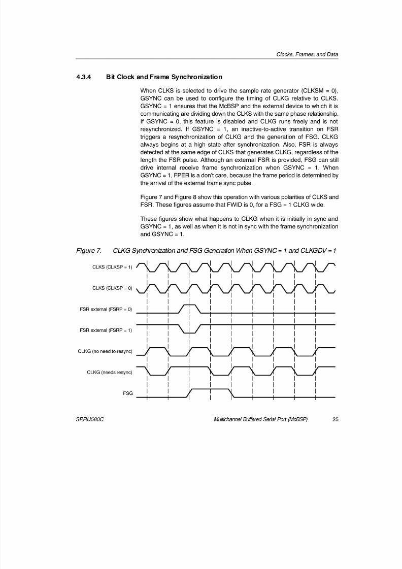
4.3.4 Bit Clock and Frame Synchronization
When CLKS is selected to drive the sample rate generator (CLKSM = 0),GSYNC can be used to configure the timing of CLKG relative to CLKS.
GSYNC = 1 ensures that the McBSP and the external device to which it is
communicating are dividing down the CLKS with the same phase relationship.
If GSYNC = 0, this feature is disabled and CLKG runs freely and is not
resynchronized. If GSYNC = 1, an inactive-to-active transition on FSR
triggers a resynchronization of CLKG and the generation of FSG. CLKG
always begins at a high state after synchronization. Also, FSR is always
detected at the same edge of CLKS that generates CLKG, regardless of the
length the FSR pulse. Although an external FSR is provided, FSG can still
drive internal receive frame synchronization when GSYNC = 1. When
GSYNC = 1, FPER is a don’t care, because the frame period is determined by
the arrival of the external frame sync pulse.
Figure 7 and Figure 8 show this operation with various polarities of CLKS and
FSR. These figures assume that FWID is 0, for a FSG = 1 CLKG wide.
These figures show what happens to CLKG when it is initially in sync and
GSYNC = 1, as well as when it is not in sync with the frame synchronization
and GSYNC = 1.
Figure 7. CLKG Synchronization and FSG Generation When GSYNC = 1 and CLKGDV = 1
FSR external (FSRP = 1)
FSG
CLKG (needs resync)
CLKG (no need to resync)
FSR external (FSRP = 0)
CLKS (CLKSP = 0)
CLKS (CLKSP = 1)

8/7/2019 McBSP Reference Guide- spru580c
http://slidepdf.com/reader/full/mcbsp-reference-guide-spru580c 26/120
Clocks, Frames, and Data
Multichannel Buffered Serial Port (McBSP)26 SPRU580C
Figure 8. CLKG Synchronization and FSG Generation When GSYNC = 1 and CLKGDV = 3
FSR external (FSRP = 1)
FSG
CLKG (needs resync)
CLKG (no need to resync)
FSR external (FSRP = 0)
CLKS (CLKSP = 0)
CLKS (CLKSP = 1)
When GSYNC = 1, the transmitter can operate synchronously with the receiver,
provided that the following conditions are met:
- FSX is programmed to be driven by the sample rate generator frame sync,FSG (FSGM = 1 in SRGR and FSXM = 1 in PCR). If the input FSR has
timing that enables it to be sampled by the falling edge of CLKG, it can be
used instead by setting FSXM = 0 in PCR and connecting FSR to FSX
externally.
- The sample-rate generator clock should drive the transmit and receive bit
clock (CLK(R/X)M = 1 in SPCR). Therefore, the CLK(R/X) pin should not
be driven by any other source.
4.3.5 Digital Loopback Mode: DLB
Setting DLB = 1 in SPCR enables digital loopback mode. In DLB mode, DR,
FSR, and CLKR are internally connected through multiplexers to DX, FSX, andCLKX, respectively, as shown in Figure 3 (page 19) and Figure 40 (page 61).
DLB mode allows testing of serial port code with a single DSP device. DLB
mode cannot be used when the McBSP is in clock stop mode (CLKSTP = 1x
in SPCR). CLKX and FSX must be enabled as outputs (CLKXM = FSXM = 1)
in DLB mode.

8/7/2019 McBSP Reference Guide- spru580c
http://slidepdf.com/reader/full/mcbsp-reference-guide-spru580c 27/120
Clocks, Frames, and Data
27Multichannel Buffered Serial Port (McBSP)SPRU580C
4.3.6 Receive Clock Selection: DLB, CLKRM
Table 4 shows how the digital loopback bit (DLB) and the CLKRM bit in PCRselect the receiver clock. In digital loopback mode (DLB = 1), the transmitter
clock drives the receiver. CLKRM determines whether the CLKR pin is an input
or an output.
Table 4. Receive Clock Selection
DLB Bit
in SPCR
CLKRM Bit
in PCR Source of Receive Clock CLKR Function
0 0 CLKR acts as an input driven by theexternal clock and inverted asdetermined by CLKRP before being
used.
Input.
0 1 The sample rate generator clock(CLKG) drives CLKR.
Output. CLKG inverted as determined byCLKRP before being driven out on CLKR.
1 0 CLKX_int drives the receive clockCLKR_int as selected and isinverted. See Table 5.
High impedance.
1 1 CLKX_int drives CLKR_int asselected and is inverted. SeeTable 5.
Output. CLKR (same as CLKX) invertedas determined by CLKRP before beingdriven out.
4.3.7 Transmit Clock Selection: CLKXM
Table 5 shows how the CLKXM bit in PCR selects the transmit clock and
whether the CLKX pin is an input or output.
Table 5. Transmit Clock Selection
CLKXM Bit
in PCR Source of Transmit Clock CLKX Function
0 The external clock drives the CLKX inputpin. CLKX is inverted as determined by
CLKXP before being used.
Input.
1 The sample rate generator clock, CLKG,drives the transmit clock
Output. CLKG is inverted as determined byCLKXP before being driven out on CLKX.

8/7/2019 McBSP Reference Guide- spru580c
http://slidepdf.com/reader/full/mcbsp-reference-guide-spru580c 28/120
Clocks, Frames, and Data
Multichannel Buffered Serial Port (McBSP)28 SPRU580C
4.3.8 Stopping Clocks
There are two methods to stop serial clocks between data transfers. Onemethod is using the SPI CLKSTP mode where clocks are stopped between
single-element transfers. This is described in section 9.
The other method is when the clocks are inputs to the McBSP (CLKXM or
CLKRM = 0) and the McBSP operates in non-SPI mode. This means that
clocks can be stopped between data transfers. If the external device stops the
serial clock between data transfers, the McBSP interprets it as a slow-down
serial clock. Ensure that there are no glitches on the CLK(R/X) lines as the
McBSP may interpret them as clock-edge transitions. Restarting the serial
clock is equivalent to a normal clock transition after a slow CLK(R/X) cycle.
Note that just as in normal operations, transmit under flow (XEMPTY) may
occur if the DXR is not properly serviced at least three CLKX cycles before thenext frame sync. Therefore if the serial clock is stopped before DXR is properly
serviced, the external device needs to restart the clock at least three CLKX
cycles before the next frame sync to allow the DXR write to be properly
synchronized. Refer to Figure 34 (page 56) for a graphical explanation on
when DXR needs to be written to avoid underflow.
4.4 Frame Sync Generation
Data frame synchronization is independently programmable for the receiver
and the transmitter for all data delay values. When set to 1, the FRST bit in
SPCR activates the frame generation logic to generate frame sync signals,
provided that FSGM = 1 in SRGR. The frame sync programming options are:
- A frame pulse with a programmable period between sync pulses and a
programmable active width specified in the sample rate generator register
(SRGR).
- The transmitter can trigger its own frame sync signal that is generated by
a DXR-to-XSR copy. This causes a frame sync to occur on every
DXR-to-XSR copy. The data delays can be programmed as required.
However, maximum packet frequency cannot be achieved in this method
for data delays of 1 and 2.
- Both the receiver and transmitter can independently select an external frame
synchronization on the FSR and FSX pins, respectively.

8/7/2019 McBSP Reference Guide- spru580c
http://slidepdf.com/reader/full/mcbsp-reference-guide-spru580c 29/120
Clocks, Frames, and Data
29Multichannel Buffered Serial Port (McBSP)SPRU580C
4.4.1 Frame Period (FPER) and Frame Width (FWID)
The FPER block is a 12-bit down counter that can count down the generateddata clocks from 4095 to 0. FPER controls the period of active frame sync
pulses. The FWID block in the sample rate generator is an 8-bit down counter.
The FWID field controls the active width of the frame sync pulse.
When the sample rate generator comes out of reset, FSG is in an inactive (low)
state. After this, when FRST = 1 and FSGM = 1, frame sync signals are
generated. The frame width value (FWID + 1) is counted down on every CLKG
cycle until it reaches 0 when FSG goes low. Thus, the value of FWID + 1
determines an active frame pulse width ranging from 1 to 256 data bit clocks.
At the same time, the frame period value (FPER + 1) is also counting down,
and when this value reaches 0, FSG goes high again, indicating a new frame
is beginning. Thus, the value of FPER + 1 determines a frame length from 1to 4096 data bits. When GSYNC = 1, the value of FPER does not matter.
Figure 9 shows a frame of 16 CLKG periods (FPER = 15 or 0000 1111b).
Figure 9. Programmable Frame Period and Width
19181716151413121110987654321
FSG
CLKG
Frame width: (FWID + 1) CLKG
Frame period: (FPER + 1) CLKG

8/7/2019 McBSP Reference Guide- spru580c
http://slidepdf.com/reader/full/mcbsp-reference-guide-spru580c 30/120
Clocks, Frames, and Data
Multichannel Buffered Serial Port (McBSP)30 SPRU580C
4.4.2 Receive Frame Sync Selection: DLB, FSRM, GSYNC
Table 6 shows how you can select various sources to provide the receiveframe synchronization signal. Note that in digital loopback mode (DLB = 1),
the transmit frame sync signal is used as the receive frame sync signal and
that DR is internally connected to DX.
Table 6. Receive Frame Synchronization Selection
DLB Bit
in SPCR
FSRM Bit
in PCR
GSYNC Bit
in SRGR
Source of Receive Frame
Synchronization FSR Pin Function
0 0 X External frame sync signaldrives the FSR input pin,whose signal is then invertedas determined by FSRPbefore being used as FSR_int.
Input.
0 1 0 Sample rate generator framesync signal (FSG) drivesFSR_int, FRST = 1.
Output. FSG is inverted asdetermined by FSRP beforebeing driven out on the FSR pin.
0 1 1 Sample rate generator framesync signal (FSG) drivesFSR_int, FRST = 1.
Input. The external frame syncinput on FSR is used tosynchronize CLKG andgenerate FSG.
1 0 0 FSX_int drives FSR_int. FSX
is selected as shown inTable 7.
High impedance.
1 X 1 FSX_int drives FSR_int and isselected as shown in Table 7.
Input. External FSR is not usedfor frame synchronization but isused to synchronize CLKG andgenerate FSG sinceGSYNC = 1.
1 1 0 FSX_int drives FSR_int and isselected as shown in Table 7.
Output. Receive (same astransmit) frame synchronizationis inverted as determined byFSRP before being driven out.

8/7/2019 McBSP Reference Guide- spru580c
http://slidepdf.com/reader/full/mcbsp-reference-guide-spru580c 31/120
Clocks, Frames, and Data
31Multichannel Buffered Serial Port (McBSP)SPRU580C
4.4.3 Transmit Frame Sync Selection: FSXM, FSGM
Table 7 shows how you can select the source of the transmit framesynchronization signal. The three choices are:
- External frame sync input
- The sample rate generator frame sync signal, FSG
- A signal that indicates a DXR-to-XSR copy has been made
Table 7. Transmit Frame Synchronization Selection
FSXM Bit
in PCR
FSGM Bit
in SRGR
Source of Transmit Frame
Synchronization FSX Pin Function
0 X External frame sync input on the FSXpin. This is inverted by FSXP beforebeing used as FSX_int.
Input.
1 1 Sample rate generator frame syncsignal (FSG) drives FSX_int.FRST = 1.
Output. FSG is inverted by FSXPbefore being driven out on FSX.
1 0 A DXR-to-XSR copy activates transmit
frame sync signal.
Output. 1-bit-clock-wide signal
inverted as determined by FSXPbefore being driven out on FSX.
4.4.4 Frame Detection for Initialization
To facilitate detection of frame synchronization, the receive and transmit CPU
interrupts (RINT and XINT) can be programmed to detect frame
synchronization by setting RINTM = XINTM = 10b in SPCR. Unlike other
types of serial port interrupts, this one can operate while the associated portion
of the serial port is in reset (for example, RINT can be activated while the
receiver is in reset). In that case, the FS(R/X)M and FS(R/X)P still select the
appropriate source and polarity of frame synchronization. Thus, even when
the serial port is in reset, these signals are synchronized to the CPU clock and
then sent to the CPU in the form of RINT and XINT at the point at which they
feed the receive and transmit portions of the serial port. A new frame
synchronization pulse can be detected, after which the CPU can safely take
the serial port out of reset.
8/7/2019 McBSP Reference Guide- spru580c
http://slidepdf.com/reader/full/mcbsp-reference-guide-spru580c 32/120
Clocks, Frames, and Data
Multichannel Buffered Serial Port (McBSP)32 SPRU580C
4.5 Data and Frames
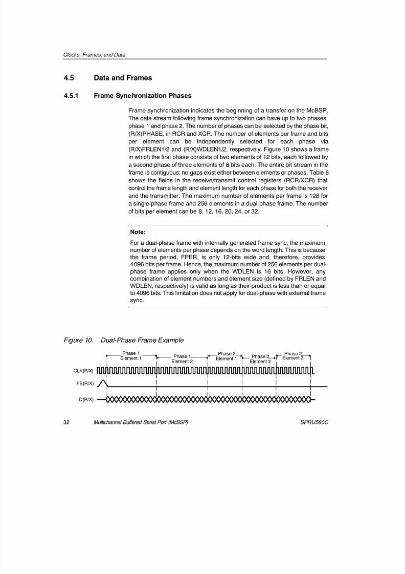
4.5.1 Frame Synchronization Phases
Frame synchronization indicates the beginning of a transfer on the McBSP.
The data stream following frame synchronization can have up to two phases,
phase 1 and phase 2. The number of phases can be selected by the phase bit,
(R/X)PHASE, in RCR and XCR. The number of elements per frame and bits
per element can be independently selected for each phase via
(R/X)FRLEN1/2 and (R/X)WDLEN1/2, respectively. Figure 10 shows a frame
in which the first phase consists of two elements of 12 bits, each followed by
a second phase of three elements of 8 bits each. The entire bit stream in the
frame is contiguous; no gaps exist either between elements or phases. Table 8
shows the fields in the receive/transmit control registers (RCR/XCR) thatcontrol the frame length and element length for each phase for both the receiver
and the transmitter. The maximum number of elements per frame is 128 for
a single-phase frame and 256 elements in a dual-phase frame. The number
of bits per element can be 8, 12, 16, 20, 24, or 32.
Note:
For a dual-phase frame with internally generated frame sync, the maximumnumber of elements per phase depends on the word length. This is becausethe frame period, FPER, is only 12-bits wide and, therefore, provides4096 bits per frame. Hence, the maximum number of 256 elements per dual-
phase frame applies only when the WDLEN is 16 bits. However, anycombination of element numbers and element size (defined by FRLEN andWDLEN, respectively) is valid as long as their product is less than or equalto 4096 bits. This limitation does not apply for dual-phase with external framesync.
Figure 10. Dual-Phase Frame Example
D(R/X)
FS(R/X)
CLK(R/X)
Element 3Phase 2
Element 2Phase 2Element 1
Phase 2
Element 2Phase 1Element 1
Phase 1
Á Á
Á
Á
Á Á
Á Á
Á Á
Á Á
Á
Á
Á Á
Á Á
Á
Á
Á
Á
Á Á
Á Á
Á Á
Á Á
Á
Á
Á Á
Á Á
Á
Á
Á
Á
Á
Á
Á Á
Á Á
Á
Á
Á Á
Á Á
Á Á
Á Á
Á
Á
Á Á
Á Á
Á
Á
Á
Á
Á Á
Á Á
Á Á
Á Á
Á
Á
Á
Á
Á Á
Á Á
Á
Á
Á Á
Á Á
Á Á
Á Á
Á
Á
Á
Á
Á Á
Á Á
Á
Á
Á Á
Á Á
Á
Á
Á Á
Á Á
Á Á
Á Á
Á
Á
Á Á
Á Á
Á
Á
Á
Á
Á
Á
Á
Á
Á Á
Á Á
Á Á
Á Á
Á
Á
Á
Á
Á Á
Á Á
Á Á
Á Á
Á
Á

8/7/2019 McBSP Reference Guide- spru580c
http://slidepdf.com/reader/full/mcbsp-reference-guide-spru580c 33/120
Clocks, Frames, and Data
33Multichannel Buffered Serial Port (McBSP)SPRU580C
Table 8. RCR/XCR Fields Controlling Elements per Frame and Bits per Element
RCR/XCR Field Controler a or
McBSP0/1 Frame Phase Elements per Frame Bits per Element
Receive 1 RFRLEN1 RWDLEN1
Receive 2 RFRLEN2 RWDLEN2
Transmit 1 XFRLEN1 XWDLEN1
Transmit 2 XFRLEN2 XWDLEN2
4.5.2 Frame Length: RFRLEN1/2, XFRLEN1/2
Frame length specifies the maximum number of serial elements or logical time
slots or channels that are available for transfer per frame synchronization
signal. In multichannel selection mode, the frame length value is independent
of (and perhaps different from) the actual number of channels that the DSP is
programmed to receive or transmit per frame via the MCR, RCER, and XCER
registers. See section 8 for details on multichannel selection mode operation.
The 7-bit (R/X)FRLEN1/2 bits in (R/X)CR support up to 128 elements per
phase in a frame, as shown in Table 9. (R/X)PHASE = 0 selects a
single-phase data frame, and (R/X)PHASE = 1 selects a dual-phase frame for
the data stream. For a single-phase frame, the value of (R/X)FRLEN2 does
not matter. Program the frame length fields with (w minus 1), where w
represents the number of elements per frame. For Figure 10,
(R/X)FRLEN1 = 1 or 000 0001b and (R/X)FRLEN2 = 2 or 000 0010b.
Table 9. Receive/Transmit Frame Length Configuration
(R/X)PHASE (R/X)FRLEN1 (R/X)FRLEN2 Frame Length
0 0 ≤ n ≤ 127 x Single-phase frame; (n+1) elements per frame
1 0 ≤ n ≤ 127 0 ≤ m ≤ 127 Dual-phase frame; (n+1) plus (m+1) elements perframe

8/7/2019 McBSP Reference Guide- spru580c
http://slidepdf.com/reader/full/mcbsp-reference-guide-spru580c 34/120
Clocks, Frames, and Data
Multichannel Buffered Serial Port (McBSP)34 SPRU580C
4.5.3 Element Length: RWDLEN1/2, XWDLEN1/2
The (R/X)WDLEN1/2 fields in the receive/transmit control register (RCR and
XCR) determine the element length in bits per element for the receiver and the
transmitter for each phase of the frame, as indicated in Table 8. Table 10 shows
how the value of these fields selects particular element lengths in bits. For the
example in Figure 10, (R/X)WDLEN1 = 001b and (R/X)WDLEN2 = 000b. If
(R/X)PHASE = 0, indicating a single-phase frame, (R/X)WDLEN2 is not used
by the McBSP and its value does not matter.
Table 10. Receive/Transmit Element Length Configuration
(R/X)WDLEN1/2 Element Length (Bits)
000 8
001 12
010 16
011 20
100 24
101 32
110 Reserved
111 Reserved
4.5.4 Data Packing using Frame Length and Element Length
The frame length and element length can be manipulated to effectively pack
data. For example, consider a situation in which four 8-bit elements are
transferred in a single-phase frame, as shown in Figure 11. In this case:
- (R/X)PHASE = 0, indicating a single-phase frame
- (R/X)FRLEN1 = 000 0011b, indicating a 4-element frame- (R/X)WDLEN1 = 000b, indicating 8-bit elements
In this example, four 8-bit data elements are transferred to and from the McBSP
by the CPU or the DMA/EDMA controller. Four reads of DRR and four writes of
DXR are necessary for each frame.
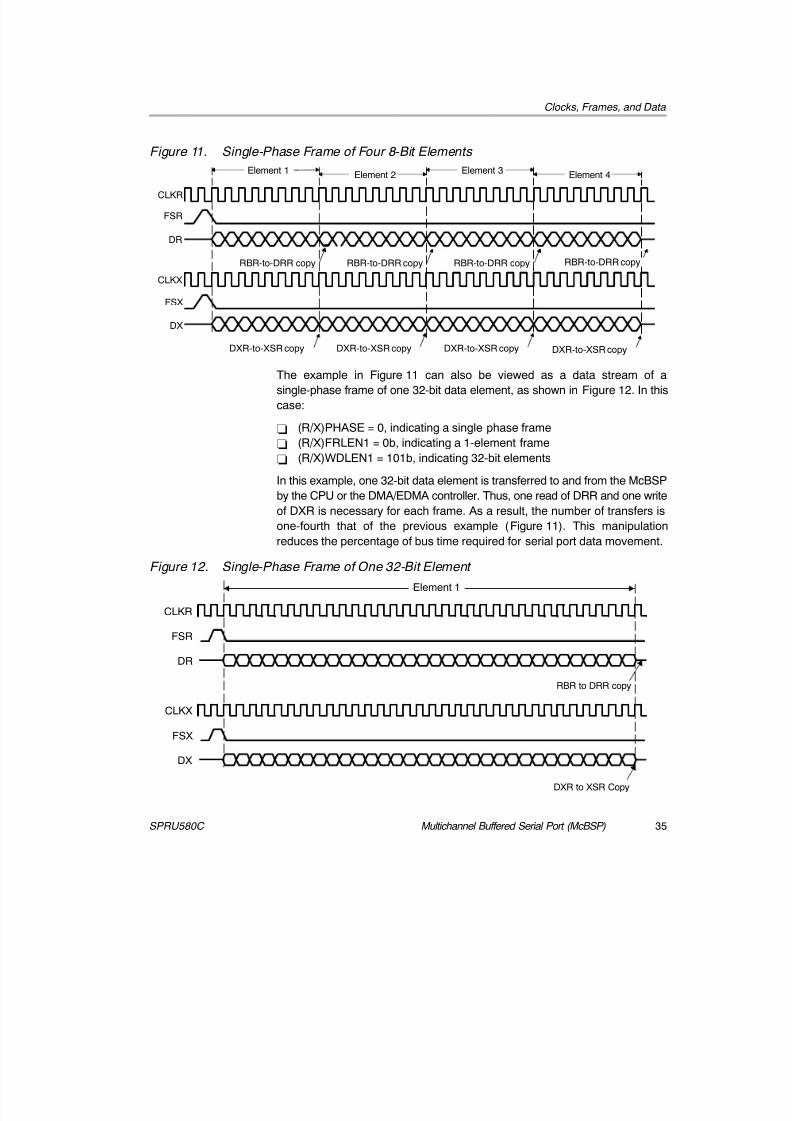
8/7/2019 McBSP Reference Guide- spru580c
http://slidepdf.com/reader/full/mcbsp-reference-guide-spru580c 35/120
Clocks, Frames, and Data
35Multichannel Buffered Serial Port (McBSP)SPRU580C
Figure 11. Single-Phase Frame of Four 8-Bit Elements
DX
FSX
CLKX
DR
FSR
CLKR
Element 4
Element 3
Element 2
Element 1
DXR-to-XSR copyDXR-to-XSR copyDXR-to-XSR copyDXR-to-XSR copy
Á
Á
Á
Á
Á Á
Á Á
Á
Á
Á Á
RBR-to-DRR copy RBR-to-DRR copyRBR-to-DRR copy RBR-to-DRR copy
The example in Figure 11 can also be viewed as a data stream of a
single-phase frame of one 32-bit data element, as shown in Figure 12. In this
case:
- (R/X)PHASE = 0, indicating a single phase frame
- (R/X)FRLEN1 = 0b, indicating a 1-element frame
- (R/X)WDLEN1 = 101b, indicating 32-bit elements
In this example, one 32-bit data element is transferred to and from the McBSP
by the CPU or the DMA/EDMA controller. Thus, one read of DRR and one write
of DXR is necessary for each frame. As a result, the number of transfers is
one-fourth that of the previous example (Figure 11). This manipulation
reduces the percentage of bus time required for serial port data movement.
Figure 12. Single-Phase Frame of One 32-Bit Element
Element 1
DXR to XSR Copy
RBR to DRR copy
CLKR
FSR
DR
CLKX
FSX
DX

8/7/2019 McBSP Reference Guide- spru580c
http://slidepdf.com/reader/full/mcbsp-reference-guide-spru580c 36/120
Clocks, Frames, and Data
Multichannel Buffered Serial Port (McBSP)36 SPRU580C
4.5.5 Data Delay: RDATDLY, XDATDLY
The start of a frame is defined by the first clock cycle in which framesynchronization is active. The beginning of actual data reception or
transmission with respect to the start of the frame can be delayed if required.
This delay is called data delay. RDATDLY and XDATDLY specify the data delay
for reception and transmission, respectively. The range of programmable data
delay is zero to two bit clocks ((R/X)DATDLY = 00b to10b), as shown in
Figure 13. Typically, a 1-bit delay is selected because data often follows a
1-cycle active frame sync pulse.
Figure 13. Data Delay
B5B6B7
B4B5B6B7
B3B4B5B6B7
D(R/X)data delay 2
data delay 1D(R/X)
data delay 0D(R/X)
FS(R/X)
CLK(R/X)
Á
Á
Á
Á
Á
Á
0-bit period
2-bit period
1-bit period
Normally a frame sync pulse is detected or sampled with respect to an edge
of serial clock CLK(R/X). Thus, on a subsequent cycle (depending on data
delay value), data can be received or transmitted. However, in the case of a
0-bit data delay, the data must be ready for reception and/or transmission on
the same serial clock cycle. For reception, this problem is solved by receive
data being sampled on the first falling edge of CLKR when an active (high) FSR
is detected. However, data transmission must begin on the rising edge of
CLKX that generated the frame synchronization. Therefore, the first data bit
is assumed to be in the XSR and DX. The transmitter then asynchronously
detects the frame synchronization, FSX goes active, and it immediately startsdriving the first bit to be transmitted on the DX pin.

8/7/2019 McBSP Reference Guide- spru580c
http://slidepdf.com/reader/full/mcbsp-reference-guide-spru580c 37/120
Clocks, Frames, and Data
37Multichannel Buffered Serial Port (McBSP)SPRU580C
Another common operation uses a data delay of 2. This configuration allows
the serial port to interface to different types of T1 framing devices in which the
data stream is preceded by a framing bit. During the reception of such a streamwith a data delay of two bits, the framing bit appears after a 1-bit delay and data
appears after a 2-bit delay). The serial port essentially discards the framing bit
from the data stream, as shown in Figure 14. In transmission, by delaying the
first transfer bit, the serial port essentially inserts a blank period (high-impedance
period) in place of the framing bit. Here, it is expected that the framing device
inserts its own framing bit or that the framing bit is generated by another
device. Alternatively, you may pull up or pull down DX to achieve the desired
value.
Figure 14. 2-Bit Data Delay Used to Discard Framing Bit
B7 B6 B5
2 Bit Periods
Framing Bit
CLKR
FSR
DR
4.5.6 Receive Data Justification and Sign Extension: RJUST
RJUST in SPCR selects whether data in RBR is right- or left-justified (with
respect to the MSB) in the DRR. If right justification is selected, RJUST furtherselects whether the data is sign-extended or zero-filled. Table 11 summarizes
the effect that various values of RJUST have on an example 12-bit receive
data value ABCh.
Table 11. Effect of RJUST Bit Values With 12-Bit Example Data ABCh
RJUST bits value Justification Extension Value in DRR
00 Right Zero-fill MSBs 0000 0ABCh
01 Right Sign-extend MSBs FFFF FABCh
10 Left Zero-fill LSBs ABC0 0000h
11 Reserved Reserved Reserved

8/7/2019 McBSP Reference Guide- spru580c
http://slidepdf.com/reader/full/mcbsp-reference-guide-spru580c 38/120
Clocks, Frames, and Data
Multichannel Buffered Serial Port (McBSP)38 SPRU580C
4.5.7 32-Bit Bit Reversal: RWDREVRS, XWDREVRS
The 32-bit bit reversal feature is only available on the C621x/C671x/C64xDSP. Normally all transfers are sent and received with the MSB first. However,
you can reverse the receive/transmit bit ordering of a 32-bit element (LSB first)
by setting all of the following:
- (R/X)WDREVRS = 1 in the receive/transmit control register (RCR/XCR).
- (R/X)COMPAND = 01b in RCR/XCR.
- (R/X)WDLEN(1/2) = 101b in RCR/XCR to indicate 32-bit elements.
When you set the register fields as above, the bit ordering of the 32-bit element
is reversed before being received by or sent from the serial port. If the
(R/W)WDREVRS and (R/X)COMPAND fields are set as indicated above, but
the element size is not set to 32-bit, operation is undefined.
4.6 Clocking and Framing Examples
4.6.1 Multiphase Frame Example: AC97
Figure 15 shows an example of the Audio Codec ’97 (AC97) standard, which
uses the dual-phase frame feature. The first phase consists of a single 16-bit
element. The second phase consists of 12 20-bit elements. The phases are
configured as follows:
- (R/X)PHASE = 1b: specifying a dual-phase frame
- (R/X)FRLEN1 = 0b: specifying one element per frame in phase 1
- (R/X)WDLEN1 = 010b: specifying 16 bits per element in phase 1
- (R/X)FRLEN2 = 000 1011b: specifying 12 elements per frame in phase 2- (R/X)WDLEN2 = 011b: specifying 20 bits per element in phase 2
- CLK(R/X)P = 0: specifying that the receive data sampled on the falling
edge of CLKR and the transmit data are clocked on the rising edge of CLKX
- FS(R/X)P = 0: indicating that active frame sync signals are used
- (R/X)DATDLY = 01b: indicating a data delay of one bit clock
Figure 15. AC97 Dual-Phase Frame Format
D(R/X)
FS(R/X)
P2E12P2E11P2E10P2E9P2E8P2E7P2E6P2E5P2E4P2E3P2E2P2E1P1E1
20 bits
16 bits
1-bit data delay
Á
Á Legend: PxEy = phase x and element y.

8/7/2019 McBSP Reference Guide- spru580c
http://slidepdf.com/reader/full/mcbsp-reference-guide-spru580c 39/120
Clocks, Frames, and Data
39Multichannel Buffered Serial Port (McBSP)SPRU580C
Figure 15 shows the AC97 timing near frame synchronization. First the frame
sync pulse itself overlaps the first element. In McBSP operation, the
inactive-to-active transition of the frame synchronization signal actuallyindicates frame synchronization. For this reason, frame synchronization can
be high for an arbitrary number of bit clocks. Only after the frame
synchronization is recognized as inactive and then active again is the next
frame synchronization recognized.
In Figure 16, there is a 1-bit data delay. Regardless of the data delay,
transmission can occur without gaps. The last bit of the previous (last) element
in phase 2 is immediately followed by the first data bit of the first element in
phase 1 of the next data frame.
Figure 16. AC97 Bit Timing Near Frame Synchronization
1-bit data delay
P2E12B1 P1E1B12P1E1B13P1E1B14P1E1B15P2E12B0DR
FSR
CLKR
Legend: PxEyBz = phase x, element y, and bit z.

8/7/2019 McBSP Reference Guide- spru580c
http://slidepdf.com/reader/full/mcbsp-reference-guide-spru580c 40/120
Clocks, Frames, and Data
Multichannel Buffered Serial Port (McBSP)40 SPRU580C
4.6.2 Double-Rate ST-BUS Clock
Figure 17 shows the McBSP timing to be compatible with the Mitel ST-BUS.The operation is running at maximum frame frequency.
- CLK(R/X)M = 1: CLK(R/X)_int generated internally by the sample rate
generator
- GSYNC = 1: CLKG is synchronized with the external frame sync signal
input on FSR. CLKG is not synchronized (it runs freely) until the frame sync
signal is active. Also, FSR is regenerated internally to form a minimum
pulse width.
- CLKSM = 0: external clock (CLKS) drives the sample rate generator
- CLKSP = 1: falling edge of CLKS generates CLKG and thus CLK(R/X)_int
- CLKGDV = 1: receive clock (shown as CLKR) is half of CLKS frequency
- FS(R/X)P = 1: active (low) frame sync pulse
- (R/X)FRLEN1 = 11111b: 32 elements per frame
- (R/X)WDLEN1 = 0: 8-bit element
- (R/X)PHASE = 0: single-phase frame and
(R/X)FRLEN2 = (R/X)WDLEN2 = X
- (R/X)DATDLY = 0: no data delay
Figure 17. Double-Rate ST-BUS Clock Example
Sample point
E2B7E1B0E1B1E1B2E1B3E1B4E1B5E1B6E1B7
E2B7E1B0E1B1E1B2E1B3E1B4E1B5E1B6E1B7
E32B0
2.048-MHz CLKG,CLKR_int,
CLKX_int (first FSR)
DR, DX(subsequent FSR)
CLKG, CLKR_int,CLKX_int
(subsequent FSR)
DR, DX (first FSR)
FSG, FSR_int,FSX_int
FSR external
4.096-MHz CLKS

8/7/2019 McBSP Reference Guide- spru580c
http://slidepdf.com/reader/full/mcbsp-reference-guide-spru580c 41/120
Clocks, Frames, and Data
41Multichannel Buffered Serial Port (McBSP)SPRU580C
4.6.3 Single-Rate ST-BUS Clock
The example in Figure 18 is the same as the ST-BUS example, except for thefollowing items:
- CLKGDV = 0: CLKS drives CLK(R/X)_int without any divide down
(single-rate clock).
- CLKSP = 0: The rising edge of CLKS generates internal clocks CLKG and
CLK(R/X)_int.
The rising edge of CLKS detects the external FSR. This external frame sync
pulse resynchronizes the internal McBSP clocks and generates the frame
sync for internal use. The internal frame sync is generated so that it is wide
enough to be detected on the falling edge of the internal clocks.
Figure 18. Single-Rate ST-BUS Clock Example
E2B7E1B0E1B1E1B2E1B3E1B4E1B5E1B6E1B7
E2B7E1B0E1B1E1B2E1B3E1B4E1B5E1B6E1B7
E32B0
CLKG, CLKR_int,
CLKX_int (first FSR)
DR, DX(subsequent FSR)
CLKG, CLKR_int,CLKX_int
(subsequent FSR)
DR, DX (first FSR)
FSG, FSR_int, FSX_int
FSR external
CLKS
Sample point

8/7/2019 McBSP Reference Guide- spru580c
http://slidepdf.com/reader/full/mcbsp-reference-guide-spru580c 42/120
Clocks, Frames, and Data
Multichannel Buffered Serial Port (McBSP)42 SPRU580C
4.6.4 Double-Rate Clock
The example in Figure 19 is the same as the ST-BUS example, except for thefollowing:
- CLKSP = 0: The rising edge of CLKS generates CLKG and CLK(R/X).
- CLKGDV = 1: CLKG, CLKR_int, and CLKX_int frequencies are half of the
CLKS frequency.
- GSYNC = 0: CLKS drives CLKG. CLKG runs freely and is not
resynchronized by FSR.
- FS(R/X)M = 0: Frame synchronization is externally generated. The
framing pulse is wide enough to be detected.
- FS(R/X)P = 0: Active (high) input frame sync signal.
- (R/X)DATDLY = 1: Specifies a data delay of one bit.
Figure 19. Double-Rate Clock Example
E2B7E1B0E1B1E1B2E1B3E1B4E1B5E1B6E1B7E32B0
CLK(R/X)_int
D(R/X)
FS(R/X)_int
CLKS

8/7/2019 McBSP Reference Guide- spru580c
http://slidepdf.com/reader/full/mcbsp-reference-guide-spru580c 43/120
McBSP Standard Operation
43Multichannel Buffered Serial Port (McBSP)SPRU580C
5 McBSP Standard Operation
During a serial transfer, there are typically periods of serial port inactivitybetween packets or transfers. The receive and transmit frame synchronization
pulse occurs for every serial transfer. When the McBSP is not in the reset state
and has been configured for the desired operation, a serial transfer can be
initiated by programming (R/X)PHASE = 0 for a single-phase frame with the
required number of elements programmed in (R/X)FRLEN1. The number of
elements can range from 1 to 128 ((R/X)FRLEN1 = 00h to 7Fh). The required
serial element length is set in the (R/X)WDLEN1 field in the (R/X)CR. If a
dual-phase frame is required for the transfer, RPHASE = 1 and each
(R/X)FRLEN1/2 can be set to any value between 0h and 7Fh.
Figure 20 shows a single-phase data frame of one 8-bit element. Since the
transfer is configured for a 1-bit data delay, the data on the DX and DR pinsare available one bit clock after FS(R/X) goes active. This figure, as well as all
others in this section, use the following assumptions:
- (R/X)PHASE = 0, specifying a single-phase frame
- (R/X)FRLEN1 = 0b, specifying one element per frame
- (R/X)WDLEN1 = 000b, specifying eight bits per element
- (R/X)FRLEN2 = (R/X)WDLEN2 = Value is ignored
- CLK(R/X)P = 0, specifying that the receive data is clocked on the falling
edge and that transmit data is clocked on the rising edge
- FS(R/X)P = 0, specifying that active (high) frame sync signals are used
- (R/X)DATDLY = 01b, specifying a 1-bit data delay
Figure 20. McBSP Standard Operation
Á Á Á Á Á Á Á Á Á Á Á Á Á Á Á Á Á Á Á Á Á Á Á Á Á Á
Á Á Á Á Á Á Á Á Á Á Á Á Á Á Á Á Á Á Á Á Á Á Á Á Á Á
Á Á Á Á Á Á Á Á Á Á Á Á Á Á Á Á Á Á Á Á Á Á Á Á Á Á
Á Á Á Á Á Á Á Á Á Á Á Á Á Á Á Á Á Á Á Á Á Á Á Á Á Á
D(R/X)
FS(R/X)
C5C6C7B0B2B3B4B5B6B7 A0 A1 B1
CLK(R/X)
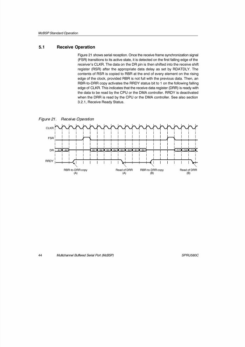
8/7/2019 McBSP Reference Guide- spru580c
http://slidepdf.com/reader/full/mcbsp-reference-guide-spru580c 44/120
McBSP Standard Operation
Multichannel Buffered Serial Port (McBSP)44 SPRU580C
5.1 Receive Operation
Figure 21 shows serial reception. Once the receive frame synchronization signal(FSR) transitions to its active state, it is detected on the first falling edge of the
receiver’s CLKR. The data on the DR pin is then shifted into the receive shift
register (RSR) after the appropriate data delay as set by RDATDLY. The
contents of RSR is copied to RBR at the end of every element on the rising
edge of the clock, provided RBR is not full with the previous data. Then, an
RBR-to-DRR copy activates the RRDY status bit to 1 on the following falling
edge of CLKR. This indicates that the receive data register (DRR) is ready with
the data to be read by the CPU or the DMA controller. RRDY is deactivated
when the DRR is read by the CPU or the DMA controller. See also section
3.2.1, Receive Ready Status.
Figure 21. Receive Operation
Á Á Á Á Á Á Á Á Á Á Á Á Á Á Á Á Á Á Á Á Á Á Á Á Á Á Á
Á Á Á Á Á Á Á Á Á Á Á Á Á Á Á Á Á Á Á Á Á Á Á Á Á Á Á
Á Á Á Á Á Á Á Á Á Á Á Á Á Á Á Á Á Á Á Á Á Á Á Á Á Á Á
Á Á Á Á Á Á Á Á Á Á Á Á Á Á Á Á Á Á Á Á Á Á Á Á Á Á Á
Read of DRR(B)
RBR-to-DRR copy(B)
Read of DRR(A)
RBR-to-DRR copy(A)
RRDY
DR
FSR
C5C6C7B0B2B3B4B5B6B7 A0 A1 B1
CLKR

8/7/2019 McBSP Reference Guide- spru580c
http://slidepdf.com/reader/full/mcbsp-reference-guide-spru580c 45/120
McBSP Standard Operation
45Multichannel Buffered Serial Port (McBSP)SPRU580C
5.2 Transmit Operation
Once transmit frame synchronization occurs, the value in the transmit shiftregister (XSR) is shifted out and driven on the DX pin after the appropriate data
delay as set by XDATDLY. XRDY is activated after every DXR-to-XSR copy on
the following falling edge of CLKX, indicating that the data transmit register
(DXR) can be written with the next data to be transmitted. XRDY is deactivated
when the DXR is written by the CPU or the DMA controller. Figure 22 illustrates
serial transmission. See section 5.5.4 for information on transmit operation
when the transmitter is pulled out of reset (XRST = 1). See also section 3.2.2,
Transmit Ready Status.
Figure 22. Transmit Operation
Á Á Á Á Á Á Á Á Á Á Á Á Á Á Á Á Á Á Á Á Á Á Á Á Á Á Á
Write of DXR
(D)
DXR to XSR copy
(C)
Write of DXR
(C)
XRDY
DX
FSX
C5C6C7B0B2B3B4B5B6B7 A0 A1
Á Á Á Á Á Á Á Á Á Á Á Á Á Á Á Á Á Á Á Á Á Á Á Á Á Á Á
B1
CLKX
DXR to XSR copy
(B)

8/7/2019 McBSP Reference Guide- spru580c
http://slidepdf.com/reader/full/mcbsp-reference-guide-spru580c 46/120
McBSP Standard Operation
Multichannel Buffered Serial Port (McBSP)46 SPRU580C
5.3 Maximum Frame Frequency
The frame frequency is determined by the following equation, which calculatesthe period between frame synchronization signals:
Frame frequency +Bit *clock frequency
Number of bit clocks between frame sync signals
The frame frequency may be increased by decreasing the time between frame
synchronization signals in bit clocks (which is limited only by the number of bits
per frame). As the frame transmit frequency is increased, the inactivity period
between the data frames for adjacent transfers decreases to 0. The minimum
time between frame synchronization pulses is the number of bits transferred
per frame. This time also defines the maximum frame frequency, which is
calculated by the following equation:
Maximum frame frequency +Bit *clock frequency
Number of bits per frame
Figure 23 shows the McBSP operating at maximum frame frequency. The
data bits in consecutive frames are transmitted continuously with no inactivity
between bits. If there is a 1-bit data delay, as shown, the frame synchronization
pulse overlaps the last bit transmitted in the previous frame.
Figure 23. Maximum Frame Frequency for Transmit and Receive
Á Á Á Á Á Á Á Á Á Á Á Á Á Á Á Á Á Á Á Á Á Á Á Á Á Á
Á Á Á Á Á Á Á Á Á Á Á Á Á Á Á Á Á Á Á Á Á Á Á Á Á Á
Á Á
Á Á
A2D(R/X)
FS(R/X)
C6C7B0B2B3B4B5B6B7 A0 A1 B1
CLK(R/X)
Note:
For (R/X)DATDLY = 0, the first bit of data transmitted is asynchronous toCLKX, as shown in Figure 13.

8/7/2019 McBSP Reference Guide- spru580c
http://slidepdf.com/reader/full/mcbsp-reference-guide-spru580c 47/120
McBSP Standard Operation
47Multichannel Buffered Serial Port (McBSP)SPRU580C
5.4 Frame Synchronization Ignore
The McBSP can be configured to ignore transmit and receive framesynchronization pulses. The (R/X)FIG bit in (R/X)CR can be cleared to 0 to
recognize frame sync pulses, or it can be set to 1 to ignore frame sync pulses.
In this way, you can use (R/X)FIG either to pack data, if operating at maximum
frame frequency, or to ignore unexpected frame sync pulses.
5.4.1 Frame Sync Ignore and Unexpected Frame Sync Pulses
RFIG and XFIG are used to ignore unexpected internal or external frame sync
pulses. Any frame sync pulse is considered unexpected if it occurs one or more
bit clocks earlier than the programmed data delay from the end of the previous
frame specified by ((R/X)DATDLY). Setting the frame ignore bits to 1 causes
the serial port to ignore these unexpected frame sync signals.
In reception, if not ignored (RFIG = 0), an unexpected FSR pulse discards the
contents of RSR in favor of the incoming data. Therefore, if RFIG = 0, an
unexpected frame synchronization pulse aborts the current data transfer, sets
RSYNCERR in SPCR to 1, and begins the reception of a new data element.
When RFIG = 1, the unexpected frame sync pulses are ignored.
In transmission, if not ignored (XFIG = 0), an unexpected FSX pulse aborts the
ongoing transmission, sets the XSYNCERR bit in SPCR to 1, and reinitiates
transmission of the current element that was aborted. When XFIG = 1,
unexpected frame sync signals are ignored.
Figure 24 shows that element B is interrupted by an unexpected frame syncpulse when (R/X)FIG = 0. The reception of B is aborted (B is lost), and a new
data element (C) is received after the appropriate data delay. This condition
causes a receive synchronization error and thus sets the RSYNCERR bit.
However, for transmission, the transmission of B is aborted and the same data
(B) is retransmitted after the appropriate data delay. This condition is a transmit
synchronization error and thus sets the XSYNCERR bit. Synchronization
errors are discussed in sections 5.5.2 and 5.5.5.

8/7/2019 McBSP Reference Guide- spru580c
http://slidepdf.com/reader/full/mcbsp-reference-guide-spru580c 48/120
McBSP Standard Operation
Multichannel Buffered Serial Port (McBSP)48 SPRU580C
Figure 24. Unexpected Frame Synchronization With (R/X)FIG = 0
A0
Current data retransmitted
New data received
(R/X)SYNCERR
DX C6C7B0B1B2B3B4B5B6B7B6B7 A0
DR
FS(R/X)
D6D7C0C2C3C4C5C6C7B6B7 C1
CLK(R/X)
Frame sync aborts current transfer
Figure 25 shows McBSP operation when unexpected internal or external
frame synchronization signals are ignored by setting (R/X)FIG = 1. Here, the
transfer of element B is not affected by an unexpected frame synchronization.
Figure 25. Unexpected Frame Synchronization With (R/X)FIG = 1
(R/X)SYNCERR(low)
A0D(R/X)
FS(R/X)
C4C5C6B0B1B2B3B4B5B6B7 C7
CLK(R/X)
Frame synchronization ignored

8/7/2019 McBSP Reference Guide- spru580c
http://slidepdf.com/reader/full/mcbsp-reference-guide-spru580c 49/120
McBSP Standard Operation
49Multichannel Buffered Serial Port (McBSP)SPRU580C
5.4.2 Data Packing using Frame Sync Ignore Bits
Section 4.5.4 describes one method of changing the element length and framelength to simulate 32-bit serial element transfers, thus requiring much less bus
bandwidth than four 8-bit transfers require. This example works when there
are multiple elements per frame. Now consider the case of the McBSP
operating at maximum packet frequency, as shown in Figure 26. Here, each
frame has only a single 8-bit element. This stream takes one read transfer and
one write transfer for each 8-bit element. Figure 27 shows the McBSP
configured to treat this stream as a continuous stream of 32-bit elements. In
this example, (R/X)FIG is set to 1 to ignore unexpected subsequent frames.
Only one read transfer and one write transfer is needed every 32-bits. This
configuration effectively reduces the required bus bandwidth to one-fourth of
the bandwidth needed to transfer four 8-bit blocks.
Figure 26. Maximum Frame Frequency Operation With 8-Bit Data
DXR-to-XSR copyDXR-to-XSR copyDXR-to-XSR copy DXR-to-XSR copy
DX
FSX
CLKX
Element 4Element 3Element 2
DR
Element 1
FSR
CLKR
RBR-to-DRR copyRBR-to-DRR copy RBR-to-DRR copyRBR-to-DRR copy

8/7/2019 McBSP Reference Guide- spru580c
http://slidepdf.com/reader/full/mcbsp-reference-guide-spru580c 50/120
McBSP Standard Operation
Multichannel Buffered Serial Port (McBSP)50 SPRU580C
Figure 27. Data Packing at Maximum Frame Frequency With (R/X)FIG = 1
Frame ignored
Frame ignored
Frame ignored
Frame ignored
Frame ignored
Frame ignored
DXR-to-XSR copy
DX
FSX
CLKX
RBR-to-DRR copy
DR
Element 1
FSR
CLKR
5.5 Serial Port Exception Conditions
There are five serial port events that can constitute a system error:
- Receive overrun (RFULL = 1)
- Unexpected receive frame synchronization (RSYNCERR = 1)
- Transmit data overwrite
- Transmit empty (XEMPTY = 0)
- Unexpected transmit frame synchronization (XSYNCERR = 1)
5.5.1 Receive Overrun: RFULL
RFULL = 1 in SPCR indicates that the receiver has experienced overrun andis in an error condition. RFULL is set when the following conditions are met:
- DRR has not been read since the last RBR-to-DRR transfer.
- RBR is full and an RBR-to-DRR copy has not occurred.
- RSR is full and an RSR-to-RBR transfer has not occurred.

8/7/2019 McBSP Reference Guide- spru580c
http://slidepdf.com/reader/full/mcbsp-reference-guide-spru580c 51/120
McBSP Standard Operation
51Multichannel Buffered Serial Port (McBSP)SPRU580C
The data arriving on DR is continuously shifted into RSR. Once a complete
element is shifted into RSR, an RSR-to-RBR transfer can occur only if an
RBR-to-DRR copy is complete. Therefore, if DRR has not been read by theCPU or the DMA controller since the last RBR-to-DRR transfer (RRDY = 1),
an RBR-to-DRR copy does not take place until RRDY = 0. This prevents an
RSR-to-RBR copy. New data arriving on the DR pin is shifted into RSR, and
the previous contents of RSR is lost. After the receiver starts running from
reset, a minimum of three elements must be received before RFULL can be
set, because there was no last RBR-to-DRR transfer before the first element.
This data loss can be avoided if DRR is read no later than two and a half CLKR
cycles before the end of the third element (data C) in RSR, as shown in
Figure 29.
Either of the following events clears the RFULL bit to 0 and allows subsequenttransfers to be read properly:
- Reading DRR
- Resetting the receiver (RRST = 0) or the device
Another frame synchronization is required to restart the receiver.
Figure 28 shows the receive overrun condition. Because element A is not read
before the reception of element B is complete, B is not transferred to DRR yet.
Another element, C, arrives and fills RSR. DRR is finally read, but not earlier
than two and one half cycles before the end of element C. New data D
overwrites the previous element C in RSR. If RFULL is still set after the DRR
is read, the next element can overwrite D if DRR is not read in time.
Figure 28. Serial Port Receive Overrun
D7 A1 A0 B7 B6 B5 B4 B3 B2 B1 B0 C7 C6 C5 C4 C3 C2 C1 C0
No RBR-to-DRR copy (B)
RBR-to-DRR copy (A)
No RSR-to-RBR copy(C)No Read of DRR(A)
CLKR
FSR
DR
RRDY
RFULLNo Read of DRR (A)

8/7/2019 McBSP Reference Guide- spru580c
http://slidepdf.com/reader/full/mcbsp-reference-guide-spru580c 52/120
McBSP Standard Operation
Multichannel Buffered Serial Port (McBSP)52 SPRU580C
Figure 29 shows the case in which RFULL is set but the overrun condition is
averted by reading the contents of DRR at least two and a half cycles before
the next element, C, is completely shifted into RSR. This ensures that aRBR-to-DRR copy of data B occurs before the next element is transferred from
RSR to RBR.
Figure 29. Serial Port Receive Overrun Avoided
A1 A0 B7 B6 B5 B4 B3 B2 B1 B0 C7 C6 C5 C4 C3 C2 C1 C0
CLKR
FSR
DR
RRDY
RFULL RBR-to-DRR (B)
Read of DRR (A)RBR-to-DRR copy (A)
No Read of DRR (A) No RBR-to-DRR copy (B)
5.5.2 Unexpected Receive Frame Synchronization: RSYNCERR
Figure 30 shows the decision tree that the receiver uses to handle all incoming
frame synchronization pulses. The diagram assumes that the receiver has
been activated (RRST = 1). Unexpected frame sync pulses can originate from
an external source or from the internal sample rate generator. An unexpected
frame sync pulse is defined as a sync pulse which occurs RDATDLY bit clocks
earlier than the last transmitted bit of the previous frame. Any one of three
cases can occur:
- Case 1: Unexpected FSR pulses with RFIG = 1. This case is discussedin section 5.4.1 and shown in Figure 25. Here, receive frame sync pulses
are ignored and the reception continues.
- Case 2: Normal serial port reception. There are three reasons for a receive
not to be in progress:
J This FSR is the first after RRST = 1.
J This FSR is the first after DRR has been read clearing an RFULL
condition.
J The serial port is in the inter-packet intervals. The programmed data
delay (RDATDLY) for reception may start during these inter-packet
intervals for the first bit of the next element to be received. Thus, at
maximum frame frequency, frame synchronization can still be
received RDATDLY bit clocks before the first bit of the associated
element.
For this case, reception continues normally, because these are not
unexpected frame sync pulses.

8/7/2019 McBSP Reference Guide- spru580c
http://slidepdf.com/reader/full/mcbsp-reference-guide-spru580c 53/120
McBSP Standard Operation
53Multichannel Buffered Serial Port (McBSP)SPRU580C
- Case 3: Unexpected receive frame synchronization with RFIG = 0
(unexpected frame not ignored). This case was shown in Figure 24 for
maximum packet frequency. Figure 31 shows this case during normaloperation of the serial port with time intervals between packets.
Unexpected frame sync pulses are detected when they occur the value in
RDATDLY bit clocks before the last bit of the previous element is received
on DR. In both cases, RSYNCERR in SPCR is set. RSYNCERR can be
cleared only by receiver reset or by writing a 0 to this bit in SPCR. If
RINTM = 11b in SPCR, RSYNCERR drives the receive interrupt (RINT)
to the CPU.
Note:
Note that the RSYNCERR bit in SPCR is a read/write bit, so writing a 1 to it
sets the error condition. Typically, writing a 0 is expected.
Figure 30. Decision Tree Response to Receive Frame Synchronization Pulse
No
Yes
No
Yes
RFIG = 1 ?
Unexpectedframe sync
pulse ?
Start next reception.Previous element is lost.
Normal reception
Set RSYNCERR. Abort reception.
Ignore frame pulse.Receiver continues running.
Start receiving data
sync pulse occursReceive frame
Case 1:
Case 2:
Case 3:

8/7/2019 McBSP Reference Guide- spru580c
http://slidepdf.com/reader/full/mcbsp-reference-guide-spru580c 54/120
McBSP Standard Operation
Multichannel Buffered Serial Port (McBSP)54 SPRU580C
Figure 31. Unexpected Receive Synchronization Pulse
Á Á Á Á Á Á Á Á Á Á Á Á Á Á Á Á Á Á Á Á Á Á Á Á Á
Á Á Á Á Á Á Á Á Á Á Á Á Á Á Á Á Á Á Á Á Á Á Á Á Á Á
Á Á Á Á Á Á Á Á Á Á Á Á Á Á Á Á Á Á Á Á Á Á Á Á Á
Á Á Á Á Á Á Á Á Á Á Á Á Á Á Á Á Á Á Á Á Á Á Á Á Á
Á Á Á Á Á Á Á Á Á Á Á Á Á Á Á Á Á Á Á Á Á Á Á Á Á Á
Á Á Á Á Á Á Á Á Á Á Á Á Á Á Á Á Á Á Á Á Á Á Á Á Á Á
RSYNCERR
RRDY
DR
FSR
C1 C0B7 A0
CLKR
Unexpected frame synchronization
RBR-to-DRR copyRead of DRR
B6 B5 B4 C7 C6 C5 C4 C3 C2 A1
RBR-to-DRR copyRead of DRR
5.5.3 Transmit With Data Overwrite
Figure 32 shows what happens if the data in DXR is overwritten before it is
transmitted. Suppose you load the DXR with data C. A subsequent write to the
DXR overwrites C with D before C is copied to the XSR. Thus, C is never
transmitted on DX. The CPU can avoid overwriting data by polling XRDY
before writing to DXR or by waiting for a programmed XINT to be triggered by
XRDY (XINTM = 00b). The DMA/EDMA controller can avoid overwriting by
synchronizing data writes with XEVT. See also the last paragraph in section
3.2.2.
Figure 32. Transmit With Data Overwrite
Á Á Á Á Á Á Á Á Á Á Á Á Á Á Á Á Á Á Á Á Á Á Á Á Á
Á Á Á Á Á Á Á Á Á Á Á Á Á Á Á Á Á Á Á Á Á Á Á Á Á
Write of DXR (D)
D6D7B0B1B2B3B4B5B6 A1
Write of DXR (E)DXR-to-XSR copy (D)Write of DXR (C)
XRDY
DX
FSX
B7 A0
CLKX
DXR-to-XSR copy (B)

8/7/2019 McBSP Reference Guide- spru580c
http://slidepdf.com/reader/full/mcbsp-reference-guide-spru580c 55/120
McBSP Standard Operation
55Multichannel Buffered Serial Port (McBSP)SPRU580C
5.5.4 Transmit Empty: XEMPTY
XEMPTY indicates whether the transmitter has experienced under flow. Eitherof the following conditions causes XEMPTY to become active (XEMPTY = 0):
- During transmission, DXR has not been loaded since the last DXR-to-XSR
copy, and all bits of the data element in XSR have been shifted out on DX.
- The transmitter is reset (XRST = 0 or the device is reset), and then
restarted.
During underflow condition, the transmitter continues to transmit the old data
in DXR for every new frame sync signal FSX (generated by an external device,
or by the internal sample rate generator) until a new element is loaded into
DXR by the CPU or the DMA/EDMA controller. XEMPTY is deactivated
(XEMPTY = 1) when this new element in DXR is transferred to XSR. In thecase when the FSX is generated by a DXR-to-XSR copy (FSXM = 1 in PCR
and FSGM = 0 in SRGR), the McBSP does not generate any new frame sync
until new data is written to the DXR and a DXR-to-XSR copy occurs.
When the transmitter is taken out of reset (XRST = 1), it is in a transmit ready
(XRDY = 1) and transmit empty (XEMPTY = 0) condition. If DXR is loaded by
the CPU or the DMA controller before FSX goes active, a valid DXR-to-XSR
transfer occurs. This allows for the first element of the first frame to be valid
even before the transmit frame sync pulse is generated or detected.
Alternatively, if a transmit frame sync is detected before DXR is loaded, 0s are
output on DX.
Figure 33 shows a transmit underflow condition. After B is transmitted, B isretransmitted on DX if you fail to reload the DXR before the subsequent frame
synchronization. Figure 34 shows the case of writing to DXR just before a
transmit underflow condition that would otherwise occur. After B is transmitted,
C is written to DXR before the next transmit frame sync pulse occurs.
Figure 33. Transmit Empty
Á Á Á Á Á Á Á Á Á Á Á Á Á Á Á Á Á Á Á Á Á Á Á Á Á Á
Á Á Á Á Á Á Á Á Á Á Á Á Á Á Á Á Á Á Á Á Á Á Á
B4B5
XEMPTY
B6B7B0B1B2B3B4B5B6 A1
XRDY
DX
FSX
B7 A0
CLKX
Write of DXR (C)DXR-to-XSR copy (B)

8/7/2019 McBSP Reference Guide- spru580c
http://slidepdf.com/reader/full/mcbsp-reference-guide-spru580c 56/120
McBSP Standard Operation
Multichannel Buffered Serial Port (McBSP)56 SPRU580C
Figure 34. Transmit Empty Avoided
Á Á Á Á Á Á Á Á Á Á Á Á Á Á Á Á Á Á Á Á Á Á Á Á Á Á Á
Á Á Á Á Á Á Á Á Á Á Á Á Á Á Á Á Á Á Á Á Á Á Á Á Á Á Á
XEMPTY
XRDY
DX
FSX
CLKX
DXR-to-XSR copy (B)
Write of DXR (C)
C5C6C7B0B1B2B3B4B5B6 A1 B7 A0
DXR-to-XSR copy (C)
5.5.5 Unexpected Transmit Frame Synchronization: XSYNCERR
A transmit frame sync error (XSYNCERR) may occur the first time the
transmitter is enabled (XRST = 1) after a device reset. To avoid this, after
enabling the transmitter for the first time, the following procedure must be
followed:
1) Wait for two CLKG cycles. The unexpected frame sync error
(XSYNCERR), if any, occurs within this time period.
2) Disable the transmitter (XRST = 0). This clears any XSYNCERR.
3) Reenable the transmitter (XRST = 1).
See also section 7 for details on initialization procedure.
Figure 35 shows the decision tree that the transmitter uses to handle all
incoming frame synchronization signals. The diagram assumes that the
transmitter has been started (XRST = 1). An unexpected transmit frame sync
pulse is defined as a sync pulse that occurs XDATDLY bit clocks earlier than the
last transmitted bit of the previous frame. Any one of three cases can occur:
- Case 1: Unexpected FSX pulses with XFIG = 1. This case is discussed in
section 5.4.1 and shown in Figure 25. In this case, unexpected FSX
pulses are ignored, and the transmission continues.

8/7/2019 McBSP Reference Guide- spru580c
http://slidepdf.com/reader/full/mcbsp-reference-guide-spru580c 57/120
McBSP Standard Operation
57Multichannel Buffered Serial Port (McBSP)SPRU580C
- Case 2: FSX pulses with normal serial port transmission. This situation is
discussed in section 5.3. There are two possible reasons for a transmit not
to be in progress:
J This FSX pulse is the first one to occur after XRST = 1.
J The serial port is in the interpacket intervals. The programmed data
delay (XDATDLY) may start during these interpacket intervals before
the first bit of the next element is transmitted. Thus, if operating at
maximum packet frequency, frame synchronization can still be
received XDATDLY bit clocks before the first bit of the associated
element.
- Case 3: Unexpected transmit frame synchronization with XFIG = 0. The
case for frame synchronization with XFIG = 0 at maximum packet
frequency is shown in Figure 24. Figure 36 shows the case for normaloperation of the serial port with interpacket intervals. In both cases,
XSYNCERR in SPCR is set. XSYNCERR can be cleared only by
transmitter reset or by writing a 0 to this bit in SPCR. If XINTM = 11b in
SPCR, XSYNCERR drives the receive interrupt (XINT) to the CPU.
Note:
The XSYNCERR bit in SPCR is a read/write bit, so writing a 1 to it sets the errorcondition. Typically, writing a 0 is expected.

8/7/2019 McBSP Reference Guide- spru580c
http://slidepdf.com/reader/full/mcbsp-reference-guide-spru580c 58/120
McBSP Standard Operation
Multichannel Buffered Serial Port (McBSP)58 SPRU580C
Figure 35. Decision Tree Response to Transmit Frame Synchronization Pulse
No
Yes
No
Yes
XFIG = 1 ?
Unexpectedframe sync
pulse ?
Restart current transfer.
Normal transmission
Set XSYNCERR. Abort transfer.
Ignore frame pulse.Transmitter continues running.
Start new transmit.
Transmit framesync pulse occurs.
Case 1:
Case 2:
Case 3:
Figure 36. Unexpected Transmit Frame Synchronization Pulse
A1 B2B3B4B5B6B7B4B5B6
XSYNCERR
XRDY
DX
FSX
B1 B0B7 A0
CLKX
Unexpected frame synchronization
Write of DXR (C) DXR-to-XSR (C)
Write of DXR (D)DXR-to-XSR copy (B)

8/7/2019 McBSP Reference Guide- spru580c
http://slidepdf.com/reader/full/mcbsp-reference-guide-spru580c 59/120
m-Law/A-Law Companding Hardware Operation
59Multichannel Buffered Serial Port (McBSP)SPRU580C
6 m-Law/A-Law Companding Hardware Operation
Companding (compressing and ex panding) hardware allows compressionand expansion of data in either µ-law or A-law format. The specification for
µ-law and A-law log PCM is part of the CCITT G.711 recommendation. The
companding standard employed in the United States and Japan is µ-law and
allows 14 bits of dynamic range. The European companding standard is A-law
and allows 13 bits of dynamic range. Any values outside these ranges are set
to the most positive or most negative value. Thus, for companding to work best
here, the data transferred to and from the McBSP via the CPU or the DMA
controller must be at least 16 bits wide.
The µ-law and A-law formats encode data into 8-bit code elements.
Companded data is always 8-bits-wide, so the appropriate (R/X)WDLEN1/2
must be cleared to 0, indicating an 8-bit serial data stream. If companding isenabled and either phase of the frame does not have an 8-bit element length,
companding continues as if the element length is eight bits.
When companding is used, transmit data is encoded according to the
specified companding law, and receive data is decoded to 2s-complement
format. Companding is enabled and the desired format is selected by
appropriately setting (R/X)COMPAND in the (R/X)CR, as indicated in Table 23
and Table 24. Compression occurs during the process of copying data from
DXR to XSR and expansion occurs from RBR to DRR, as shown in Figure 37.
For transmit data to be compressed, it should be 16-bit, left-justified data, such
as LAW16, as shown in Figure 38. The value can be either 13 or 14 bits wide,depending on the companding law. This 16-bit data is aligned in DXR, as
shown in Figure 39.
For reception, the 8-bit compressed data in RBR is expanded to a left-justified
16-bit data, LAW16. This can be further justified to 32-bit data by programming
the RJUST bits in SPCR, as shown in Table 12.
Figure 37. Companding Flow
Á Á Á
Á Á Á
Á Á Á
Á Á Á
Á Á Á Á
Á Á Á Á
Á Á Á Á
Á Á Á
Á Á Á
Á Á Á Á Á Á Á Á
Á Á Á Á Á
Á Á Á Á Á
Á Á Á Á Á
Á Á Á Á Á
Á Á Á Á Á
Á Á Á Á Á
168
32168
From CPU/DMADX
DR To CPU/DMA
Á Á Á
Á Á Á
Á Á Á
Á Á Á
Á Á Á
Á Á Á
DRRRJUST
DXR
Expand
Compress
RBR
XSR
RSR
µ-LAW/A-LAW Companding Hardware Operation
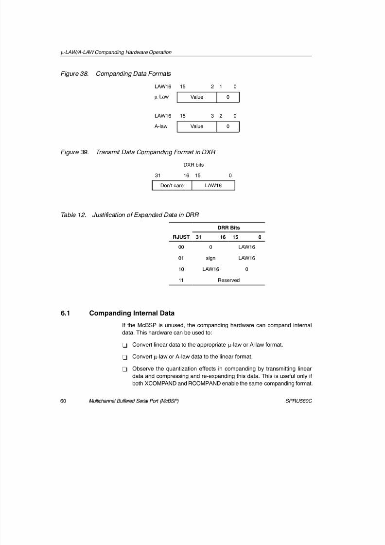
8/7/2019 McBSP Reference Guide- spru580c
http://slidepdf.com/reader/full/mcbsp-reference-guide-spru580c 60/120
m-Law/A-Law Companding Hardware Operation
Multichannel Buffered Serial Port (McBSP)60 SPRU580C
Figure 38. Companding Data Formats
LAW16 15 2 1 0
µ-Law Value 0
LAW16 15 3 2 0
A-law Value 0
Figure 39. Transmit Data Companding Format in DXR
DXR bits
31 16 15 0
Don’t care LAW16
Table 12. Justification of Expanded Data in DRR
DRR Bits
RJUST 31 16 15 0
00 0 LAW16
01 sign LAW16
10 LAW16 0
11 Reserved
6.1 Companding Internal Data
If the McBSP is unused, the companding hardware can compand internal
data. This hardware can be used to:
- Convert linear data to the appropriate µ-law or A-law format.- Convert µ-law or A-law data to the linear format.
- Observe the quantization effects in companding by transmitting linear
data and compressing and re-expanding this data. This is useful only if
both XCOMPAND and RCOMPAND enable the same companding format.
µ-LAW/A-LAW Companding Hardware Operation

8/7/2019 McBSP Reference Guide- spru580c
http://slidepdf.com/reader/full/mcbsp-reference-guide-spru580c 61/120
m-Law/A-Law Companding Hardware Operation
61Multichannel Buffered Serial Port (McBSP)SPRU580C
Figure 40 shows two methods by which the McBSP can compand internal
data. Data paths for these two methods are indicated by (DLB) and (non-DLB)
arrows.
- Non-DLB: When both the transmit and receive sections of the serial port
are reset, DRR and DXR are internally connected through the companding
logic. Values from DXR are compressed as determined by the XCOMPAND
bits and then expanded as determined by the RCOMPAND bits. RRDY
and XRDY bits are not set. However, data is available in DRR four CPU
clocks after being written to DXR. The advantage of this method is its
speed. The disadvantage is that there is no synchronization available to
the CPU and the DMA/EDMA controller to control the flow of data.
- DLB: The McBSP is enabled in digital loopback (DLB) mode with
companding appropriately enabled by the RCOMPAND and XCOMPANDbits. Receive and transmit interrupts (RINT when RINTM = 0 and XINT
when XINTM = 0) or synchronization events (REVT and XEVT) allow
synchronization of the CPU or the DMA/EDMA controller to these
conversions, respectively. Here, the time for this companding depends on
the serial bit rate selected.
Figure 40. Companding of Internal Data
Á Á Á Á
Á Á Á Á
Á Á Á
Á Á Á
Á Á Á Á
Á Á Á Á
Á Á Á
Á Á Á Á Á Á Á
Á Á Á Á
Á Á Á Á
Á Á Á Á
Á Á Á Á
Á Á Á Á
Á Á Á Á
(DLB)
From CPU orDMA/EDMA controller
DX
DR To CPU orDMA/EDMA
controller
Á Á Á Á
Á Á Á Á
Á Á Á Á
Á Á Á Á
DRRRJUST
DXR
Expand
Compress
RBR
XSR
RSR
(non-DLB)
To CPU orDMA/EDMA
controller
6.2 Bit Ordering
Normally, all transfers on the McBSP are sent and received with the MSB first.
However, certain 8-bit data protocols (that do not use companded data) require
the LSB to be transferred first. By setting the (R/X)COMPAND = 01b in
(R/X)CR, the bit ordering of 8-bit elements is reversed (LSB first) before being
sent to the serial port. Like the companding feature, this feature is enabled only
if the appropriate (R/X)WDLEN1/2 bit is cleared to 0, indicating that 8-bit
elements are to be serially transferred.
For the C621x/C671x/C64x DSP, a 32-bit bit reversal feature is also available.
See section 4.5.7.
µ-LAW/A-LAW Companding Hardware Operation

8/7/2019 McBSP Reference Guide- spru580c
http://slidepdf.com/reader/full/mcbsp-reference-guide-spru580c 62/120
McBSP Initialization Procedure
Multichannel Buffered Serial Port (McBSP)62 SPRU580C
7 McBSP Initialization Procedure
The McBSP initialization procedure varies depending on the specific systemsetup. Section 7.1 provides a general initialization sequence. Section 7.2
provides an initialization sequence for the special case when the external
device provides the transmit frame sync FSX (FSXM = 0).
The transmitter and the receiver of the McBSP can operate independently
from each other. Therefore, they can be placed in or taken out of reset individually
by modifying only the desired bit in the registers without disrupting the other
portion. The steps in the following sections discuss the initialization procedure
for taking both the transmitter and the receiver out of reset. To initialize only
one portion, configure only the portion desired.
The McBSP internal sample rate generator and internal frame sync generator
are shared between the transmitter and the receiver. Table 13 and Table 14
describe their usage base upon the clock and frame sync configurations of the
receiver and transmitter, respectively.
Table 13. Receiver Clock and Frame Configurations
CLKR source FSR source Comment on Configuration
Internal Internal The McBSP internal sample rate generator and internal frame sync generatorare used by the receiver.
External Internal Invalid configuration for receiver.
Internal External The McBSP internal sample rate generator is used but the internal framesync generator is not used by the receiver.
External External The McBSP internal sample rate generator and internal frame sync generatorare not used by the receiver.

8/7/2019 McBSP Reference Guide- spru580c
http://slidepdf.com/reader/full/mcbsp-reference-guide-spru580c 63/120
McBSP Initialization Procedure
63Multichannel Buffered Serial Port (McBSP)SPRU580C
Table 14. Transmitter Clock and Frame Configurations
CLKX source FSX source Comment on Configuration
Internal Internal The McBSP internal sample rate generator is used by the transmitter. Thetransmitter can generate frame sync FSX in one of two ways. First, it cangenerate FSX by using the internal frame sync generator (FSGM = 1).
Alternatively, it can generate FSX upon each DXR-to-XSR copy (FSGM = 0).In this case, the internal frame sync generator can be kept in reset(FRST = 0) if it is not used by the receiver. You can follow the generalinitialization sequence in section 7.1.
External Internal The McBSP internal sample rate generator and internal frame sync generatorare not used by the transmitter. This configuration is only valid with FSGM = 0where the McBSP transmitter generates FSX upon each DXR-to-XSR copy.
You can follow the general initialization sequence in section 7.1.
Internal External The McBSP internal sample rate generator is used by the transmitter but theinternal frame sync generator is not. You should follow the special initializationsequence for McBSP as transmit frame sync master in section 7.2.
External External The McBSP internal sample rate generator and internal frame sync generatorare not used by the transmitter. You should follow the special initializationsequence for McBSP as transmit frame sync master in section 7.2.
7.1 General Initialization Procedure
This section provides the general initialization procedure. For the special casewhen the transmitter is used and the transmit frame sync FSX is provided by
the external device, see section 7.2.
1) Ensure that no portion of the McBSP is using the internal sample rate
generator signal CLKG and the internal frame sync generator signal FSG
(GRST = FRST = 0). The respective portion of the McBSP needs to be in
reset (XRST = 0 and/or RRST = 0).
2) Program the control registers as required. Ensure the internal sample rate
generator and the internal frame sync generator are still in reset
(GRST = FRST = 0). Also ensure the respective portion of the McBSP is
still in reset in this step (XRST = 0 and/or RRST = 0).
3) Wait for proper internal synchronization. If the external device provides the
bit clock, wait for two CLKR or CLKX cycles. If the McBSP generates the
bit clock as a clock master, wait for two CLKSRG cycles. In this case, the
clock source to the sample rate generator (CLKSRG) is selected by the
CLKSM bit in SRGR.

8/7/2019 McBSP Reference Guide- spru580c
http://slidepdf.com/reader/full/mcbsp-reference-guide-spru580c 64/120
McBSP Initialization Procedure
Multichannel Buffered Serial Port (McBSP)64 SPRU580C
4) Skip this step if the bit clock is provided by the external device. This step
only applies if the McBSP is the bit clock master and the internal sample
rate generator is used.
a) Start the sample rate generator by setting the GRST bit to 1. Wait two
CLKG bit clocks for synchronization. CLKG is the output of the sample
rate generator.
b) On the next rising edge of CLKSRG, CLKG transitions to 1 and starts
clocking with a frequency equal to 1/(CLKGDV + 1) of the sample rate
generator source clock CLKSRG.
5) Skip this step if the transmitter is not used. If the transmitter is used, a
transmit sync error (XSYNCERR) may occur when it is enabled for the first
time after device reset. The purpose of this step is to clear any potential
XSYNCERR that occurs on the transmitter at this time:a) Set the XRST bit to 1 to enable the transmitter.
b) Wait for any unexpected frame sync error to occur. If the external
device provides the bit clock, wait for two CLKR or CLKX cycles. If the
McBSP generates the bit clock as a clock master, wait for two CLKG
cycles. The unexpected frame sync error (XSYNCERR), if any, occurs
within this time period.
c) Disable the transmitter (XRST = 0). This clears any outstanding
XSYNCERR.
6) Setup data acquisition as required:
a) If the DMA/EDMA is used to service the McBSP, setup data acquisitionas desired and start the DMA/EDMA in this step, before the McBSP
is taken out of reset.
b) If CPU interrupt is used to service the McBSP, enable the transmit
and/or receive interrupt as required.
c) If CPU polling is used to service the McBSP, no action is required in
this step.
7) Set the XRST bit and/or the RRST bit to 1 to enable the corresponding
section of the McBSP. The McBSP is now ready to transmit and/or receive.
a) If the DMA/EDMA is used to service the McBSP, it services the McBSP
automatically upon receiving the XEVT and/or REVT.
b) If CPU interrupt is used to service the McBSP, the interrupt service
routine is automatically entered upon receiving the XINT and/or RINT.
c) If CPU polling is used to service the McBSP, it can do so now by polling
the XRDY and/or RRDY bit.

8/7/2019 McBSP Reference Guide- spru580c
http://slidepdf.com/reader/full/mcbsp-reference-guide-spru580c 65/120
McBSP Initialization Procedure
65Multichannel Buffered Serial Port (McBSP)SPRU580C
8) If the internal frame sync generator is used (FSGM = 1), proceed to the
additional steps to turn on the internal frame sync generator. Initialization
is complete if any one of the following is true:
a) The external device generates frame sync FSX and/or FSR. The
McBSP is now ready to transmit and/or receive upon receiving external
frame sync.
b) The McBSP generates transmit frame sync FSX upon each
DXR-to-XSR copy. The internal frame sync generator is not used
(FSGM = 0).
Additional steps to turn on the internal frame sync generator (only applies if
FSGM = 1):
9) Skip this step if the transmitter is not used. If the transmitter is used, ensure
that DXR is serviced before you start the internal frame sync generator.
You can do so by checking XEMPTY = 1 (XSR is not empty) in SPCR.
10) Set the FRST bit to 1 to start the internal frame sync generator. The internal
frame sync signal FSG is generated on a CLKG active edge after 7 to 8
CLKG clocks have elapsed.
7.2 Special Case: External Device is the Transmit Frame Master
Care must be taken if the transmitter expects a frame sync from an external
device. After the transmitter comes out of reset (XRST = 1), it waits for a frame
sync from the external device. If the first frame sync arrives very shortly after
the transmitter is enabled, the CPU or DMA/EDMA may not have a chance toservice DXR. In this case, the transmitter shifts out the default data in XSR
instead of the desired value, which has not yet arrived in DXR. This causes
problems in some applications, as the first data element in the frame is invalid.
The data stream appears element-shifted (the first data word may appear in
the second channel instead of the first).
To ensure proper operation when the external device is the frame master, you
must assure that DXR is already serviced with the first word when a frame sync
occurs. To do so, you can keep the transmitter in reset until the first frame sync
is detected. Upon detection of the first frame sync, the McBSP generates an
interrupt to the CPU. Within the interrupt service routine, the transmitter is
taken out of reset (XRST = 1). This assures that the transmitter does not begindata transfers at the data pin during the first frame sync period. This also
provides almost an entire frame period for the DSP to service DXR with the first
word before the second frame sync occurs. The transmitter only begins data
transfers upon receiving the second frame sync. At this point, DXR is already
serviced with the first word.

8/7/2019 McBSP Reference Guide- spru580c
http://slidepdf.com/reader/full/mcbsp-reference-guide-spru580c 66/120
McBSP Initialization Procedure
Multichannel Buffered Serial Port (McBSP)66 SPRU580C
The interrupt service routine must first be setup according to the description
in step 9. Then follow this modified procedure for proper initialization:
1) Ensure that no portion of the McBSP is using the internal sample rate
generator signal CLKG and the internal frame sync generator signal FSG
(GRST = FRST = 0). The respective portion of the McBSP needs to be in
reset (XRST = 0 and/or RRST = 0).
2) Program SRGR and other control registers as required. Ensure the
internal sample rate generator and the internal frame sync generator are
still in reset (GRST = FRST = 0). Also ensure the respective portion of the
McBSP is still in reset in this step (XRST = 0 and/or RRST = 0).
3) Program the XINTM bits to 2h in SPCR to generate an interrupt to the CPU
upon detection of a transmit frame sync. Do not enable the XINT interrupt
in the interrupt enable register (IER) in this step.
4) Wait for proper internal synchronization. If the external device provides the
bit clock, wait for two CLKR or CLKX cycles. If the McBSP generates the
bit clock as a clock master, wait for two CLKSRG cycles. In this case, the
clock source to the sample rate generator (CLKSRG) is selected by the
CLKSM bit in SRGR.
5) Skip this step if the bit clock is provided by the external device. This step
only applies if the McBSP is the bit clock master and the internal sample
rate generator is used.
a) Start the sample rate generator by setting the GRST bit to 1. Wait two
CLKG bit clocks for synchronization. CLKG is the output of the samplerate generator.
b) On the next rising edge of CLKSRG, CLKG transitions to 1 and starts
clocking with a frequency equal to 1/(CLKGDV + 1) of the sample rate
generator source clock CLKSRG.
6) A transmit sync error (XSYNCERR) may occur when it is enabled for the
first time after device reset. The purpose of this step is to clear any potential
XSYNCERR that occurs on the transmitter at this time:
a) Set the XRST bit to 1 to enable the transmitter.
b) Wait for any unexpected frame sync error to occur. If the external
device provides the bit clock, wait for two CLKR or CLKX cycles. If the
McBSP generates the bit clock as a clock master, wait for two CLKG
cycles. The unexpected frame sync error (XSYNCERR), if any, occurs
within this time period.
c) Disable the transmitter (XRST = 0). This clears any outstanding
XSYNCERR.

8/7/2019 McBSP Reference Guide- spru580c
http://slidepdf.com/reader/full/mcbsp-reference-guide-spru580c 67/120
McBSP Initialization Procedure
67Multichannel Buffered Serial Port (McBSP)SPRU580C
7) Setup data acquisition as required:
a) If the DMA/EDMA is used to service the McBSP, setup data acquisitionas desired and start the DMA/EDMA in this step, before the McBSP
is taken out of reset.
b) If CPU interrupt is used to service the McBSP, no action is required in
this step.
c) If CPU polling is used to service the McBSP, no action is required in
this step.
8) Enable the XINT interrupt by setting the corresponding bit in the interrupt
enable register (IER). In this step, the McBSP transmitter is still in reset.
Upon detection of the first transmit frame sync from the external device,
the McBSP generates an interrupt to the CPU and the DSP enters the
interrupt service routine (ISR). The ISR needs to perform these tasks in
this order:
a) Modify the XINTM bits to the value desired for normal McBSP
operations. If CPU interrupt is used to service the McBSP in normal
operations, ensure that the XINTM bits are modified to 0 to detect the
McBSP XRDY event. If no McBSP interrupt is desired in normal
operations, disable future McBSP-to-CPU interrupt in the interrupt
enable register (IER).
b) Set the XRST bit and/or the RRST bit to 1 to enable the respective
portion of the McBSP. The McBSP is now ready to transmit and/or
receive.
9) Service the McBSP:
a) If CPU polling is used to service the McBSP in normal operations, it
can do so upon exit from the ISR.
b) If CPU interrupt is used to service the McBSP in normal operations,
upon XRDY interrupt service routine is entered. The ISR should be
setup to verify that XRDY = 1 and service the McBSP accordingly.
c) If DMA/EDMA is used to service the McBSP in normal operations, it
services the McBSP automatically upon receiving the XEVT and/or
REVT.
10) Upon detection of the second frame sync, DXR is already serviced and the
transmitter is ready to transmit the valid data. The receiver is also serviced
properly by the DSP.

8/7/2019 McBSP Reference Guide- spru580c
http://slidepdf.com/reader/full/mcbsp-reference-guide-spru580c 68/120
Multichannel Selection Operation
Multichannel Buffered Serial Port (McBSP)68 SPRU580C
8 Multichannel Selection Operation
The multichannel selection mode allows the McBSP to select independentchannels (elements) for transmit and receive in a single-phase frame. Each
frame represents a time-division multiplexed data stream. For all of the
McBSP, up to 32 elements in a bit stream of up to 128 elements can be enabled
at any given time. The C64x McBSP is an enhanced version that can also
select up to 128 elements at any given time (see section 8.3).
If a receive element is not enabled:
- RRDY is not set to 1 upon reception of the last bit of the element.
- RBR is not copied to DRR upon reception of the last bit of the element.
Thus, RRDY is not set active. This feature also implies that no interrupts
or synchronization events are generated for this element.
If a transmit element is not enabled:
- DX is in the high impedance state.
- A DXR-to-XSR transfer is not automatically triggered at the end of serial
transmission of the related element.
- XEMPTY and XRDY are not affected by the end of transmission of the
related serial element.
An enabled transmit element can have its data masked or transmitted. When
data is masked, the DX pin is forced to the high-impedance state even thoughthe transmit channel is enabled.
The following control registers are used in multichannel operation:
- The multichannel control register (MCR)
- The transmit channel enable register (XCER)
- The receive channel enable register (RCER)
Note:
For C64x DSP, RCER and XCER are replaced by RCERE0 and XCERE0,respectively. Additional registers XCERE1, XCERE2, XCERE3, RCERE1,
RCERE2, and RCERE3 are also used in this mode.

8/7/2019 McBSP Reference Guide- spru580c
http://slidepdf.com/reader/full/mcbsp-reference-guide-spru580c 69/120
Multichannel Selection Operation
69Multichannel Buffered Serial Port (McBSP)SPRU580C
8.1 Enabling Multichannel Selection
Multichannel mode can be enabled independently for reception andtransmission by setting the RMCM bit to 1 and the XMCM bit to a nonzero value
in MCR, respectively.
8.2 Enabling and Masking of Channels in Normal Multichannel SelectionMode
This section describes how to enable the channels in normal multichannel
selection mode. For the C64x DSP, see also section 8.3 for the enhanced
multichannel selection mode.
For all C6000 devices, a total of 32 of the available 128 elements can beenabled at any given time. The 128 elements comprise eight subframes (0
through 7), and each subframe has 16 contiguous elements. Even-numbered
subframes 0, 2, 4, and 6 belong to partition A; odd-numbered subframes 1, 3,
5, and 7 belong to partition B.
The number of elements enabled can be updated during the course of a frame
to allow any arbitrary group of elements to be enabled. This update is
accomplished using an alternating ping-pong scheme for controlling two
subframes (one odd-numbered and the other even-numbered) of 16
contiguous elements within a frame at any time. One subframe belongs to
partition A and the other to partition B.
Any one 16-element block from partition A and partition B can be selected,
yielding a total of 32 elements that can be enabled at one time. The subframes
are allocated on 16-element boundaries within the frame, as shown in
Figure 41. The (R/X)PABLK and (R/X)PBBLK fields in MCR select the
subframes in partition A and B, respectively. This enabling is performed
independently for transmit and receive.
Figure 41. Element Enabling by Subframes in Partitions A and B
112-127
3
80-95
2
48-63
1
16-31
0
0-15
0
96-111
3
64-79
2
32-47
1
0-15
0
076543210
FS(R/X)
Partition Belements
(R/X)PBBLK
Partition Aelements
(R/X)PABLK
Subframe #
Á Á Á Á Á Á Á Á Á Á Á Á Á Á Á Á Á Á Á Á Á Á Á Á Á Á
Á Á Á Á Á Á Á Á Á Á Á Á Á Á Á Á Á Á Á Á Á Á Á Á Á Á

8/7/2019 McBSP Reference Guide- spru580c
http://slidepdf.com/reader/full/mcbsp-reference-guide-spru580c 70/120
Multichannel Selection Operation
Multichannel Buffered Serial Port (McBSP)70 SPRU580C
Transmit data masking allows an element enabled for transmit to have its DX
pin set to the high-impedance state during its transmit period. In systems
where symmetric transmit and receive provides software benefits, this featureallows transmit elements to be disabled on a shared serial bus. A similar
feature is not needed for receive, because multiple receptions cannot cause
serial bus contention.
Note:
DX is masked or driven to the high-impedance state:
- During inter-packet intervals.
- When an element is masked regardless of whether it is enabled.
- When an element is disabled.
Following are descriptions of how each XMCM bit value affects operation in
normal multichannel selection mode:
- XMCM = 00b: The serial port transmits data over the DX pin for the
number of elements programmed in XFRLEN1. Thus, DX is driven during
transmit.
- XMCM = 01b: Only those elements that need to be transmitted are
selected via XP[A/B]BLK and XCER. Only these selected elements are
written to DXR and ultimately transmitted. In other words, if XINTM = 00b,
which implies that an XINT is generated for every DXR-to-XSR copy, the
number of XINT generated is equal to the number of elements selected
via XCER (and not equal to XFRLEN1).
- XMCM = 10b: All elements are enabled, which means all the elements in
a data frame (XFRLEN1) are written to DXR and DXR-to-XSR copies
occur at their respective times. However, DX is driven only for those
elements that are selected via XP[A/B]BLK and XCER and is placed in the
high-impedance state otherwise. In this case, if XINTM = 00b, the number
of interrupts generated due to every DXR-to-XSR copy would equal the
number of elements in that frame (XFRLEN1).
- XMCM = 11b: In this mode, symmetric transmit and receive operation is
forced. Select desired receive channels by setting the RCER[A/B].
Symmetric operation occurs when a device transits and receives on thesame set of subframes. These subframes are determined by setting
RP[A/B]BLK. The elements in each of these subframes can then be
enabled/selected using RCER for receive. The transmit side uses the
same blocks as the receive side (thus the value of X(P/A)BLK does not
matter). In this mode, all elements are disabled, so DR and DX are in the

8/7/2019 McBSP Reference Guide- spru580c
http://slidepdf.com/reader/full/mcbsp-reference-guide-spru580c 71/120
Multichannel Selection Operation
71Multichannel Buffered Serial Port (McBSP)SPRU580C
high-impedance state. For receiving, a RBR-to-DRR copy occurs only for
those elements that are selected via RP(A/BBLK and RCER. If RINT were
to be generated for every RBR-to-DRR copy, it would occur as many timesas the number of elements selected in RCER (and not the number of
elements programmed in RFRLEN1). For transmitting, the same
subframe that is used for reception is used to maintain symmetry, so the
value XP[A/B]BLK does not matter. DXR is loaded, and DXR-to-XSR copy
occurs for all the elements that are enabled via RP[A/B]BLK. However, DX
is driven only for those elements that are selected via XCER. The
elements enabled in XCER can be either a subset of, or the same as, those
selected in RCER. Therefore, if XINTM = 00b, transmit interrupts to the
CPU would be generated the same number of times as the number of
elements selected in RCER (not XCER).
Figure 42 shows the activity on the McBSP pins for all of the preceding XMCMbit values with the following conditions:
- (R/X)PHASE = 0: Single-phase frame for multichannel selection enabled
- FRLEN1 = 011b: 4-element frame
- WDLEN1 = Any valid serial element length
In the following illustrations, the arrows indicating the occurrence of events are
only sample indications.
Figure 42. XMCM Operation
(a) XMCM = 00b
DXR to XSR(E0)
Write of DXR(E1)
DXR-to-XSR copy(E1)
Write of DXR(E2)
DXR-to-XSR copy(E2)
DXR-to-XSR copy(E3)
E3E2E1
Write of DXR(E3)
XRDY
DX E0
FSX
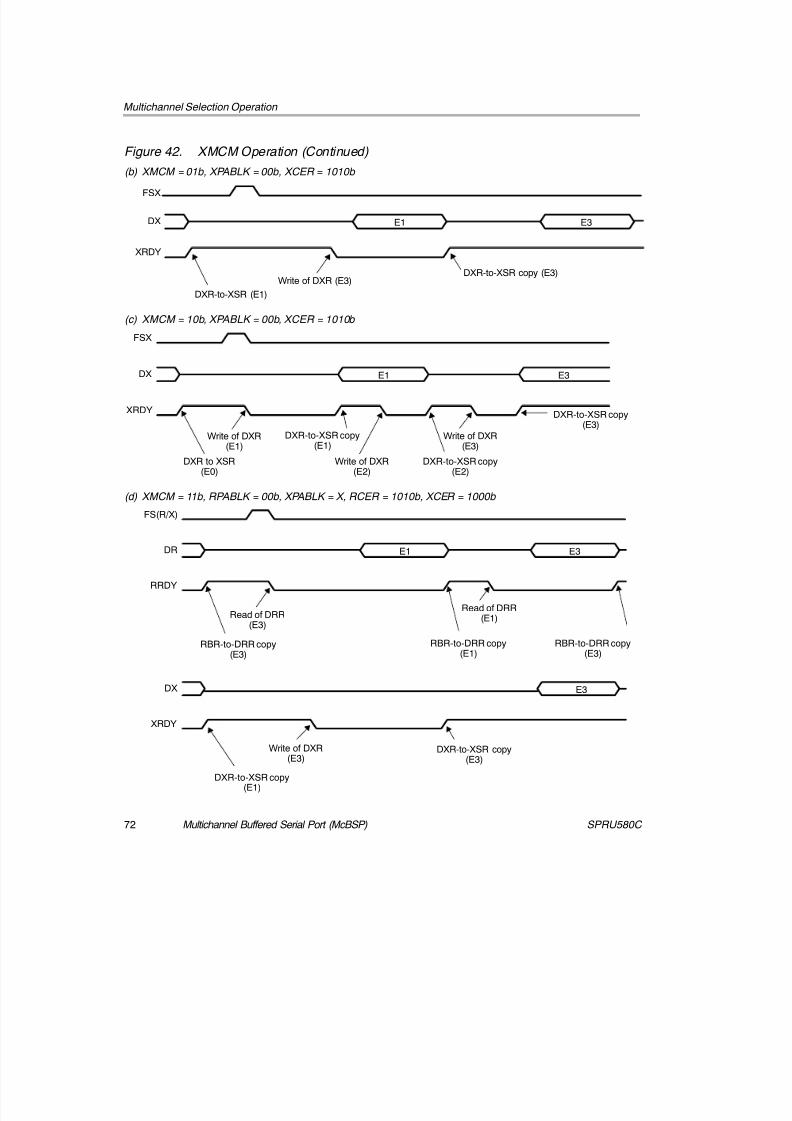
8/7/2019 McBSP Reference Guide- spru580c
http://slidepdf.com/reader/full/mcbsp-reference-guide-spru580c 72/120
Multichannel Selection Operation
Multichannel Buffered Serial Port (McBSP)72 SPRU580C
Figure 42. XMCM Operation (Continued)
(b) XMCM = 01b, XPABLK = 00b, XCER = 1010b
DXR-to-XSR (E1)
Write of DXR (E3)DXR-to-XSR copy (E3)
E3E1
XRDY
DX
FSX
(c) XMCM = 10b, XPABLK = 00b, XCER = 1010b
DXR-to-XSR copy(E3)
DXR to XSR(E0)
Write of DXR(E1)
DXR-to-XSR copy(E1)
Write of DXR(E2)
DXR-to-XSR copy(E2)
E3E1
Write of DXR(E3)
XRDY
DX
FSX
(d) XMCM = 11b, RPABLK = 00b, XPABLK = X, RCER = 1010b, XCER = 1000b
DXR-to-XSR copy(E3)
Write of DXR(E3)
DXR-to-XSR copy(E1)
Read of DRR(E1)
RBR-to-DRR copy(E3)
E3DX
XRDY
RBR-to-DRR copy(E3)
Read of DRR(E3)
RBR-to-DRR copy(E1)
E3E1
RRDY
DR
FS(R/X)

8/7/2019 McBSP Reference Guide- spru580c
http://slidepdf.com/reader/full/mcbsp-reference-guide-spru580c 73/120
Multichannel Selection Operation
73Multichannel Buffered Serial Port (McBSP)SPRU580C
8.2.1 Changing Element Selection
Using the multichannel selection feature, a static group of 32 elements can beenabled and remains enabled with no CPU intervention until this allocation is
modified. An arbitrary number of, group of, or all of the elements within a frame
can be accessed by updating the block allocation registers during the course
of the frame in response to the end-of-subframe interrupts (see section 8.2.2
for information about these interrupts).
Note:
You must be careful not to affect the currently selected subframe when chang-ing the selection.
The currently selected subframe is readable through the RCBLK and XCBLK
bits in MCR for receive and transmit, respectively. The associated channelenable register cannot be modified if it is selected by the appropriate
(R/X)P[A/B]BLK register to point toward the current subframe. Similarly, the
(R/X)PABLK and (R/X)PBBLK bits in MCR cannot be modified while pointing to
or being changed to point to the currently selected subframe. If the total number
of elements is 16 or less, the current partition is always pointed to. In this case,
only a reset of the serial port can change the element enabling.
8.2.2 End-of-Subframe Interrupt
At the end of every subframe (16 elements or less) boundary during multichannel
operation, the receive interrupt (RINT), if RINTM = 01b in SPCR, or transmit
interrupt (XINT), if XINTM = 01b in SPCR, is generated to the CPU. This
interrupt indicates that a new partition has been crossed. You can then check
the current partition and change the selection of subframes in the A and/or B
partitions if they do not point to the current subframe. These interrupts are two
CPU-clock high pulses. If RINTM = XINTM = 01b when (R/X)MCM = 0
(non-multichannel operation), interrupts are not generated.
8.3 Enhanced Multichannel Selection Mode (C64x DSP only)
In addition to the normal multichannel selection mode, the C64x McBSP has
the enhanced multichannel selection mode that allows up to 128 channels to
be enabled at any given time. The enhanced multichannel selection mode is
selected by setting the enhanced receive multichannel selection enable bit
(RMCME) and the enhanced transmit multichannel selection enable bit(XMCME) in MCR to 1. This mode works in conjunction with six additional
enhanced receive/transmit channel enable registers in the C64x McBSP:
RCERE1, RCERE2, RCERE3, XCERE1, XCERE2, and XCERE3. The RCER
and XCER described in section 11.8 are replaced by the RCERE0 and
XCERE1, respectively, in the C64x McBSP.

8/7/2019 McBSP Reference Guide- spru580c
http://slidepdf.com/reader/full/mcbsp-reference-guide-spru580c 74/120
Multichannel Selection Operation
Multichannel Buffered Serial Port (McBSP)74 SPRU580C
When the RMCME and XMCME bits are cleared to 0, the C64x McBSP is in
the normal multichannel selection mode. See section 8.2 for a detailed
description. In normal multichannel selection mode, RCERE1−
RCERE3 andXCERE1−XCERE3 are not used; RCERE0 and XCERE0 function as RCER
and XCER, respectively.
When the RMCME and XMCME bits are set to 1, the C64x McBSP has
128-channel selection capability. RCERE0−RCERE3 and XCERE0−XCERE3
are used to enable up to 128 channels. Since up to 128 channels can be
selected at one time, the (R/X)P[A/B]BLK and (R/X)CBLK values in MCR have
no effect in this mode. But, if necessary, the (R/X)CBLK value can be read to
determine the subframe that is active. Perform the following to enable up to
128 channels:
- Enable the selected channels in XCERE0−
XCERE3 and
RCERE0−RCERE3.
- Set RMCME = XMCME = 1 in MCR.
- Set RMCM and XMCM in MCR as desired.
Following are descriptions of how each XMCM bit value affects operation in
the enhanced multichannel selection mode (similar to its function in normal
multichannel selection mode):
- XMCM = 00b: The serial port transmits data over the DX pin for thenumber of elements programmed in XFRLEN1. Thus, DX is driven during
transmit.
- XMCM = 01b: Only those elements that need to be transmitted are
selected via XCERE0−XCERE3. Only these selected elements are written
to DXR and ultimately transmitted. In other words, if XINTM = 00b, which
implies that an XINT is generated for every DXR-to-XSR copy, the number
of XINT generated is equal to the number of elements selected via
XCERE0−XCERE3 (and not equal to XFRLEN1).
- XMCM = 10b: All elements are enabled, which means all the elements in
a data frame (XFRLEN1) are written to DXR and DXR-to-XSR copiesoccur at their respective times. However, DX is driven only for those
elements that are selected via XCERE0−XCERE3, and is placed in the
high-impedance state otherwise. In this case, if XINTM = 00b, the number
of interrupts generated due to every DXR-to-XSR copy would equal the
number of elements in that frame (XFRLEN1).

8/7/2019 McBSP Reference Guide- spru580c
http://slidepdf.com/reader/full/mcbsp-reference-guide-spru580c 75/120
Multichannel Selection Operation
75Multichannel Buffered Serial Port (McBSP)SPRU580C
- XMCM = 11b: In this mode, symmetric transmit and receive operation is
forced. Select the desired receive channels by setting
RCERE0−
RCERE3. The elements enabled in XCERE0−
XCERE3 can beeither a subset of or the same as those selected in RCERE0−RCERE3.
In this mode all elements are disabled, so DR and DX are in the
high-impedance state. For receiving, an RBR-to-DRR copy occurs only for
those elements that are selected via RCERE0−RCERE3. If RINT were to
be generated for every RBR-to-DRR copy, it would occur as many times
as the number of elements selected in RCERE0−RCERE3 (and not the
number of elements programmed in RFRLEN1). For transmitting, DXR is
loaded and a DXR-to-XSR copy occurs for all the elements that are
enabled via RCERE0−RCERE3. However, DX is driven only for those
elements that are selected via XCER. Therefore, if XINTM = 00b, transmit
interrupts to the CPU would be generated the same number of times as
the number of elements selected in RCERE0−
RCERE3 (not
XCERE0−XCERE3).
8.4 DX Enabler: DXENA
The DX enabler is only available for the C621x/C671x/C64x device. The
DXENA bit in SPCR controls the high impedance enable on the DX pin. When
DXENA = 1, the McBSP enables extra delay for the DX pin turn-on time. This
feature is useful for McBSP multichannel operations, such as in a time-division
multiplexed (TDM) system. The McBSP supports up to 128 channels in a
multichannel operation. These channels can be driven by different devices in
a TDM data communication line, such as the T1/E1 line. In any multichannel
operation where multiple devices transmit over the same DX line, you need to
ensure that no two devices transmit data simultaneously, which results in bus
contention. Enough dead time should exist between the transmission of the
first data bit of the current device and the transmission of the last data bit of
the previous device. In other words, the last data bit of the previous device
needs to be disabled to a high-impedance state before the next device begins
transmitting data to the same data line, as shown in Figure 43.
Figure 43. DX Timing for Multichannel Operation
B0 (processor 0)
CLKX
DX B7 (processor 1) B6 (processor 1)
Extra delayif DXENA = 1 (processor 1)
Disable time(processor 0)
Dead timeNo extra delayeven with DXENA = 1

8/7/2019 McBSP Reference Guide- spru580c
http://slidepdf.com/reader/full/mcbsp-reference-guide-spru580c 76/120
Multichannel Selection Operation
Multichannel Buffered Serial Port (McBSP)76 SPRU580C
In the case when two McBSPs are used to transmit data over the same TDM
line, bus contention occurs if DXENA = 0. The first McBSP turns off the
transmission of the last data bit (changes DX from valid to a high-impedancestate) after a disable time specified in the datasheet. As shown in Figure 43,
this disable time is measured from the CLKX active clock edge. The next
McBSP turns on its DX pin (changes from a high-impedance state to valid)
after a delay time. Again, this delay time is measured from the CLKX active
clock edge. Bus contention occurs because the dead time between the two
devices is not enough. You need to apply alternative software or hardware
methods to ensure proper multichannel operation in this case.
If you set DXENA = 1 in the second McBSP, the second McBSP turns on its
DX pin after some extra delay time. This ensures that the previous McBSP on
the same DX line is disabled before the second McBSP starts driving out data.
The DX enabler controls only the high-impedance enable on the DX pin, notthe data itself. Data is shifted out to the DX pin at the same time as in the case
when DXENA = 0. The only difference is that with DXENA = 1, the DX pin is
masked to a high-impedance state for some extra CPU cycles before the data
is seen on the TDM data line. Therefore, only the first bit of data is delayed.
Refer to the specific device datasheet for the exact amount of delay.

8/7/2019 McBSP Reference Guide- spru580c
http://slidepdf.com/reader/full/mcbsp-reference-guide-spru580c 77/120
SPI Protocol: CLKSTP
77Multichannel Buffered Serial Port (McBSP)SPRU580C
9 SPI Protocol: CLKSTP
A system conforming to the SPI protocol has a master-slave configuration.The SPI protocol is a 4-wire interface composed of serial data in (master in
slave out or MISO), serial data out (master out slave in or MOSI), shift clock
(SCK), and an active (low) slave enable (SS) signal. Communication between
the master and the slave is determined by the presence or absence of the
master clock. Data transfer is initiated by the detection of the master clock and
is terminated on absence of the master clock. The slave has to be enabled
during this period of transfer. When the McBSP is the master, the slave enable
is derived from the master transmit frame sync pulse (FSX). Example block
diagrams of the McBSP as a master and as a slave are shown in Figure 44 and
Figure 45, respectively.
Figure 44. SPI Configuration: McBSP as the Master
McBSP master
CLKX
DX
DR
FSX
SPI compliantslave
SCK
MOSI
MISO
SS
Figure 45. SPI Configuration: McBSP as the Slave
McBSP slave
CLKX
DX
DR
FSX
SPI compliant
master
SCK
MISO
MOSI
SS

8/7/2019 McBSP Reference Guide- spru580c
http://slidepdf.com/reader/full/mcbsp-reference-guide-spru580c 78/120
SPI Protocol: CLKSTP
Multichannel Buffered Serial Port (McBSP)78 SPRU580C
The clock stop mode (CLKSTP) of the McBSP provides compatibility with the
SPI protocol. The McBSP supports two SPI transfer formats that are specified
by the clock stop mode bits (CLKSTP) in SPCR. The CLKSTP bits inconjunction with the CLKXP bit in PCR allows serial clocks to be stopped
between transfers using one of four possible timing variations, as shown in
Table 15. Figure 46 and Figure 47 show the timing diagrams of the two SPI
transfer formats and the four timing variations.
Note:
The digital loopback mode (DLB = 1 in SPCR cannot be used in conjunctionwith the clock stop mode (CLKSTP = 1x).
Table 15. SPI-Mode Clock Stop Scheme
CLKSTP Bits CLKXP Bit Clock Scheme
0X X Clock stop mode is disabled. Clock is enabled for non-SPI mode.
10 0 Low inactive state without delay. The McBSP transmits data on the risingedge of CLKX and receives data on the falling edge of CLKX.
11 0 Low inactive state with delay. The McBSP transmits data one-half cycleahead of the rising edge of CLKX and receives data on the rising edge of CLKX.
10 1 High inactive state without delay. The McBSP transmits data on the fallingedge of CLKX and receives data on the rising edge of CLKX.
11 1 High inactive state with delay. The McBSP transmits data one-half cycleahead of the falling edge of CLKX and receives data on the falling edge of CLKX.
Figure 46. SPI Transfer with CLKSTP = 10b
Á Á
Á
Á
Á
Á
B1B2B4 B3 B0B5B6B7
B0B1B2B3B4B5B6B7
FSX/SS
D(R/X)/MISO(from slave)‡
D(R/X)/MOSI(from master)†
CLKX (CLKXP=1)/SCK
CLKX (CLKXP=0)/SCK
Á Á Á Á Á Á Á Á Á Á Á Á Á Á Á Á Á Á Á Á Á Á Á
Á Á Á Á Á Á Á Á Á Á Á Á Á Á Á Á Á Á Á Á Á Á Á
Á Á Á Á Á Á Á Á Á Á Á Á Á Á Á Á Á Á Á Á Á Á Á
Á Á Á Á Á Á Á Á Á Á Á Á Á Á Á Á Á Á Á Á Á Á Á
Á Á Á Á Á Á Á Á Á Á Á Á Á Á Á Á Á Á Á Á Á Á Á
† If the McBSP is the SPI master (CLKXM = 1), MOSI=DX. If the McBSP is the SPI slave (CLKXM = 0), MOSI = DR.‡ If the McBSP is the SPI master (CLKXM = 1), MISO=DR. If the McBSP is the SPI slave (CLKXM = 0), MISO = DX.

8/7/2019 McBSP Reference Guide- spru580c
http://slidepdf.com/reader/full/mcbsp-reference-guide-spru580c 79/120
SPI Protocol: CLKSTP
79Multichannel Buffered Serial Port (McBSP)SPRU580C
Figure 47. SPI Transfer with CLKSTP = 11b
Á Á Á Á Á Á Á Á Á Á Á Á Á Á Á Á Á Á Á Á Á Á Á Á
B1B2B4 B3 B0B5B6B7
B0B1B2B3B4B5B6B7
FSX/SS
D(R/X)/MISO(from slave)‡
D(R/X)/MOSI(from master)†
CLKX (CLKXP=1)/SCK
CLKX (CLKXP=0)/SCK
Á Á Á Á Á Á Á Á Á Á Á Á Á Á Á Á Á Á Á Á Á Á Á Á
Á Á
Á Á
Á
Á
Á Á Á
Á Á Á Á Á Á Á Á Á Á Á Á Á Á Á Á Á Á Á Á Á Á Á Á
Á Á Á Á Á Á Á Á Á Á Á Á Á Á Á Á Á Á Á Á Á Á Á Á
† If the McBSP is the SPI master (CLKXM = 1), MOSI=DX. If the McBSP is the SPI slave (CLKXM = 0), MOSI = DR.‡ If the McBSP is the SPI master (CLKXM = 1), MISO=DR. If the McBSP is the SPI slave (CLKXM = 0), MISO = DX.
The CLKSTP bits in SPCR and the CLKXP bit in PCR select the appropriate
clock scheme for a particular SPI interface, as shown in Table 15. The
CLKSTP and CLKXP bits determine the following conditions:
- Whether clock stop mode is enabled or not
- In clock stop mode, whether the clock is high or low when stopped
- In clock stop mode, whether the first clock edge occurs at the start of the
first data bit or at the middle of the first data bit
The CLKXP bit selects the edge on which data is transmitted (driven) and
received (sampled), as shown in Table 15.
Figure 46 is the timing diagram when CLKSTP = 10b. In this SPI transfer
format, the transition of the first clock edge (CLKX) marks the beginning of data
transfer, provided the slave enable (FSX/SS) is already asserted. Data
transfer is synchronized to the first clock edge.
Figure 47 is the timing diagram when CLKSTP = 11b. Data transfer begins
before the transition of the serial clock. Therefore, the transition of the slave
enable signal FSX/SS from high to low, instead of the transition of the serial
clock, marks the beginning of transfer in this SPI transfer format. In SPI master
mode, as well as SPI slave mode, the McBSP requires an FSX/SS edge for
each transfer. This means the FSX/SS signal must toggle for each word. The
McBSP clock stop mode requires single-phase frames ((R/X)PHASE = 0) andone element per frame ((R/X)FRLEN = 0).

8/7/2019 McBSP Reference Guide- spru580c
http://slidepdf.com/reader/full/mcbsp-reference-guide-spru580c 80/120
SPI Protocol: CLKSTP
Multichannel Buffered Serial Port (McBSP)80 SPRU580C
When the McBSP is configured to operate in SPI mode, both the transmitter
and the receiver operate together as a master or a slave. The McBSP is a
master when it generates clocks. When the McBSP is the SPI master, CLKXdrives both its own internal receive clock (CLKR) and the serial clock (SCK)
of the SPI slave. The FSR and CLKR signals should not be used in SPI mode.
These do not function as SPI signals like the FSX and CLKX signals. In
conjunction with CLKSTP enabled, CLKXM = 1 (in PCR) indicates that the
McBSP is a master, and CLKXM = 0 indicates that the McBSP is an SPI slave.
The slave enable signal (FSX/SS) enables the serial data input and output
driver on the slave device (the device not providing the output clock).
9.1 McBSP Operation as the SPI Master
When the McBSP is the SPI master, it generates the master clock CLKX and
the slave enable FSX. Therefore, CLKX should be configured as an output
(CLKXM = 1) and FSX should be configured as an output that can be
connected to the slave enable (SS) input on the slave device (FSXM = 1). The
DXR-to-XSR transfer of each element generates the slave enable FSX
(FSGM = 0 in SRGR). Therefore to receive an element in SPI master mode,
the McBSP must also simultaneously transmit an element (write to DXR) in
order to generate the necessary slave enable FSX. The FSX needs to be
asserted (low) to enable the slave before the McBSP starts shifting out data
on the DX pin. Refer to the MOSI and FSX waveforms in Figure 46 and
Figure 47. Therefore, the XDATDLY and RDATDLY bits must be programmed
to 1. When the McBSP is the SPI master, an XDATDLY value of 0 or 2 causes
undefined operation and an RDATDLY value of 0 causes the received data tobe shifted incorrectly.
As the SPI master, the McBSP generates CLKX and FSX through the internal
sample rate generator. As discussed in section 4.3.1, the CLKSM bit in SRGR
should be set to specify either the CPU clock or the external clock input (CLKS)
as the clock source to the internal sample rate generator. The CLKGDV (clock
divide ratio) in SRGR should be programmed to generate CLKX at the required
SPI data rate. The McBSP generates a continuous clock (CLKX) internally and
gates the clock off (stops the clock) to the external interface when transfers are
finished. The McBSP receive clock is provided from the internal continuously
running clock, so the receiver and transmitter both work internally as if clocks
do not stop. Selection of the clock stop modes overrides the frame generatorbit fields (FPER and FWID) in SRGR.

8/7/2019 McBSP Reference Guide- spru580c
http://slidepdf.com/reader/full/mcbsp-reference-guide-spru580c 81/120
SPI Protocol: CLKSTP
81Multichannel Buffered Serial Port (McBSP)SPRU580C
9.2 McBSP Operation as the SPI Slave
When the McBSP is an SPI slave device, the master clock CLKX and slaveenable FSX are generated by an external SPI master, as shown in Figure 45.
Thus, the CLKX and FSX pins are configured as inputs by clearing the CLKXM
and FSXM bits in PCR to 0. In SPI mode, the FSX and CLKX inputs are also
utilized as the internal FSR and CLKR signals for data reception. Data transfer
is synchronized to the master clock CLKX and the internal serial port logic
performs transfers using only the exact number of input clock pulses CLKX per
data bit. The external master needs to assert FSX (low) before the transfer of
data begins. FSX is used in its asynchronous form and it controls the McBSP
initial drive of data to the DX pin.
When the McBSP is a slave, the (R/X)DATDLY bits in the receive/transmit
control register ((R/X)CR) should be cleared to 0. XDATDLY = 0 ensures that
the first data to be transmitted is available on the DX pin. The MISO waveform
in Figure 46 and Figure 47 shows how the McBSP transmits data as an SPI
slave. RDATDLY = 0 ensures that the McBSP is ready to receive data from the
SPI master as soon as it detects the serial clock CLKX. Depending on the clock
stop mode used, data is received at various clock edges according to Table 15.
Although the CLKX signal is generated externally by the master, the internal
sample rate generator of the McBSP must be enabled for proper SPI slave
mode operation. The internal sample rate clock is then used to synchronize
the input clock (CLKX) and frame sync (FSX) from the master to the CPU
clock. Accordingly, the CLKSM bit in SRGR should be left at the default value
(CLKSM = 1) to specify the CPU clock as the clock source of the sample rate
generator. Furthermore, the CLKGDV bits in SRGR must be set to a value
such that the rate of the internal clock CLKG is at least eight times that of the
SPI data rate. This rate is achieved by programming the sample rate generator
to its maximum speed (CLKGDV = 1) for all SPI transfer rates.
9.3 McBSP Initialization for SPI Mode
The operation of the serial port during device reset, transmitter reset, and
receiver reset is described in section 3.1. For McBSP operation as a master
or a slave in SPI mode, you must follow these steps for proper initialization:
1) Set XRST = RRST = 0 in SPCR.
2) Program the necessary McBSP configuration registers (and not the data
registers) as required when the serial port is in the reset state
(XRST = RRST = 0). Write the desired value into the CLKSTP bits in
SPCR. Table 15 shows the various CLKSTP modes.
3) Set the GRST bit to 1 in SPCR to get the sample rate generator out of reset.

8/7/2019 McBSP Reference Guide- spru580c
http://slidepdf.com/reader/full/mcbsp-reference-guide-spru580c 82/120
SPI Protocol: CLKSTP
Multichannel Buffered Serial Port (McBSP)82 SPRU580C
4) Wait two bit clocks for the McBSP to reinitialize.
5) Depending upon whether the CPU or DMA services the McBSP, performstep (a) if the CPU is used, or step (b) if the DMA is used.
a) If the CPU is used to service the McBSP. set XRST = RRST = 1 to
enable the serial port. Note that the value written to SPCR at this time
should have only the reset bits changed to 1 and the remaining
bit-fields should have the same values as in Step 2 and 4 above.
b) If the DMA is used to perform data transfers, the DMA should be
initialized first with the appropriate read/write syncs and the start bit
set to run. The DMA waits for the synchronization events to occur.
Now, pull the McBSP out of reset by setting XRST = RRST = 1.
6) Wait two bit clocks for the receiver and transmitter to become active.

8/7/2019 McBSP Reference Guide- spru580c
http://slidepdf.com/reader/full/mcbsp-reference-guide-spru580c 83/120
McBSP Pins as General-Purpose I/O
83Multichannel Buffered Serial Port (McBSP)SPRU580C
10 McBSP Pins as General-Purpose I/O
Two conditions allow the serial port pins (CLKX, FSX, DX, CLKR, FSR, DR,
and CLKS) to be used as general-purpose I/O pins rather than serial port pins:
- The related portion (transmitter or receiver) of the serial port is in reset:
(R/X)RST = 0 in SPCR
- General-purpose I/O is enabled for the related portion of the serial port:
(R/X)IOEN = 1 in PCR
The PCR bits configure each of the McBSP pins as general-purpose inputs or
outputs, as shown in Table 16. In the case of FS(R/X), FS(R/X)M = 0 configures
the pin as an input and FS(R/X)M = 1 configures the pin as an output. When
configured as an output, the value driven on FS(R/X) is the value stored in
FS(R/X)P. If configured as an input, the FS(R/X)P becomes a read-only bit that
reflects the status of that signal. CLK(R/X)M and CLK(R/X)P work similarly forCLK(R/X). When the transmitter is selected as general-purpose I/O, the value
of the DXSTAT bit in PCR is driven onto DX. DR is always an input and its value
is held in the DRSTAT bit in PCR. To configure CLKS as a general-purpose
input, both the transmitter and receiver have to be in the reset state and
(R/X)IOEN has to be set to 1, because (R/X)IOEN is always an input to the
McBSP and it affects both transmit and receive operations.
Table 16. Configuration of Pins as General Purpose I/O
Output Input
Pin
General-Purpose I/O
Enabled When...
Selected as
Output When...
Output Value
Driven From
Selected as
Input When ...
Input Value
Readable onCLKX XRST = 0
XIOEN = 1CLKXM = 1 CLKXP CLKXM = 0 CLKXP
FSX XRST = 0XIOEN = 1
FSXM = 1 FSXP FSXM = 0 FSXP
DX XRST = 0XIOEN = 1
Always DX_STAT Never N/A
CLKR RRST = 0RIOEN = 1
CLKRM = 1 CLKRP CLKRM = 0 CLKRP
FSR RRST = 0
RIOEN = 1
FSRM = 1 FSRP FSRM = 0 FSRP
DR RRST = 0RIOEN = 1
Never N/A Always DR_STAT
CLKS RRST = XRST = 0RIOEN = XIOEN = 1
Never N/A Always CLKS_STAT

8/7/2019 McBSP Reference Guide- spru580c
http://slidepdf.com/reader/full/mcbsp-reference-guide-spru580c 84/120
Registers
Multichannel Buffered Serial Port (McBSP)84 SPRU580C
11 Registers
Table 17 lists the McBSP registers and their memory addresses for the
C620x/C670x DSP, Table 18 lists the McBSP registers for the
C621x/C671x DSP, and Table 19 lists the McBSP registers for the C64x DSP.
See the device-specific datasheet for the memory address of these registers.
The McBSP control registers are accessible only via the peripheral bus (see
Figure 1). You should halt the McBSP before making changes to the serial port
control register (SPCR), receive control register (RCR), transmit control
register (XCR), and pin control register (PCR). Changes made to these
registers without halting the McBSP could result in an undefined state.
Table 17. McBSP Registers for C620x/C670x DSP
McBSPs on Device (Hex Byte Address)
Acronym Register Name McBSP 0 McBSP 1 McBSP 2§ Section
RBR† Receive buffer register − − − −
RSR† Receive shift register − − − −
XSR† Transmit shift register − − − −
DRR‡
Data receive register 018C 0000 0190 0000 01A4 0000 11.1
DXR Data transmit register 018C 0004 0190 0004 01A4 0004 11.2
SPCR Serial port control register 018C 0008 0190 0008 01A4 0008 11.3
RCR Receive control register 018C 000C 0190 000C 01A4 000C 11.4
XCR Transmit control register 018C 0010 0190 0010 01A4 0010 11.5
SRGR Sample rate generator register 018C 0014 0190 0014 01A4 0014 11.6
MCR Multichannel control register 018C 0018 0190 0018 01A4 0018 11.7
RCER Receive channel enable register 018C 001C 0190 001C 01A4 001C 11.8
XCER Transmit channel enable register 018C 0020 0190 0020 01A4 0020 11.9
PCR Pin control register 018C 0024 0190 0024 01A4 0024 11.12
† The RBR, RSR, and XSR are not directly accessible via the CPU or the DMA/EDMA controller.‡ The CPU and DMA/EDMA controller can only read this register; they cannot write to it.§ Available only on C6202(B) DSP and C6203(B) DSP.

8/7/2019 McBSP Reference Guide- spru580c
http://slidepdf.com/reader/full/mcbsp-reference-guide-spru580c 85/120
Registers
85Multichannel Buffered Serial Port (McBSP)SPRU580C
Table 18. McBSP Registers for C621x/C671x DSP
McBSPs on Device
Acronym Register Name McBSP 0 McBSP 1 Section
RBR† Receive buffer register RBR0 RBR1 −
RSR† Receive shift register RSR0 RSR1 −
XSR† Transmit shift register XSR0 XSR1 −
DRRठData receive register DRR0 DRR1 11.1
DXR§ Data transmit register DXR0 DXR1 11.2
SPCR Serial port control register SPCR0 SPCR1 11.3
RCR Receive control register RCR0 RCR1 11.4
XCR Transmit control register XCR0 XCR1 11.5
SRGR Sample rate generator register SRGR0 SRGR1 11.6
MCR Multichannel control register MCR0 MCR1 11.7
RCER Receive channel enable register RCER0 RCER1 11.8
XCER Transmit channel enable register XCER0 XCER1 11.9
PCR Pin control register PCR0 PCR1 11.12
† The RBR, RSR, and XSR are not directly accessible via the CPU or the DMA/EDMA controller.‡ The CPU and DMA/EDMA controller can only read this register; they cannot write to it.
§ The DRR and DXR are accessible via the peripheral bus and via the EDMA bus.

8/7/2019 McBSP Reference Guide- spru580c
http://slidepdf.com/reader/full/mcbsp-reference-guide-spru580c 86/120
Registers
Multichannel Buffered Serial Port (McBSP)86 SPRU580C
Table 19. McBSP Registers for C64x DSP
McBSPs on Device
Acronym Register Name McBSP 0 McBSP 1 McBSP 2¶ Section
RBR† Receive buffer register RBR0 RBR1 RBR2 −
RSR† Receive shift register RSR0 RSR1 RSR2 −
XSR† Transmit shift register XSR0 XSR1 XSR2 −
DRRठData receive register DRR0 DRR1 DRR2 11.1
DXR§ Data transmit register DXR0 DXR1 DXR2 11.2
SPCR Serial port control register SPCR0 SPCR1 SPCR2 11.3
RCR Receive control register RCR0 RCR1 RCR2 11.4
XCR Transmit control register XCR0 XCR1 XCR2 11.5
SRGR Sample rate generator register SRGR0 SRGR1 SRGR2 11.6
MCR Multichannel control register MCR0 MCR1 MCR2 11.7
RCERE0 Enhanced receive channel enable register 0 RCERE00 RCERE01 RCERE02 11.10
RCERE1 Enhanced receive channel enable register 1 RCERE10 RCERE11 RCERE12 11.10
RCERE2 Enhanced receive channel enable register 2 RCERE20 RCERE21 RCERE22 11.10
RCERE3 Enhanced receive channel enable register 3 RCERE30 RCERE31 RCERE32 11.10
XCERE0 Enhanced transmit channel enable register 0 XCERE00 XCERE01 XCERE02 11.11
XCERE1 Enhanced transmit channel enable register 1 XCERE10 XCERE11 XCERE12 11.11
XCERE2 Enhanced transmit channel enable register 2 XCERE20 XCERE21 XCERE22 11.11
XCERE3 Enhanced transmit channel enable register 3 XCERE30 XCERE31 XCERE32 11.11
PCR Pin control register PCR0 PCR1 PCR2 11.12
† The RBR, RSR, and XSR are not directly accessible via the CPU or the DMA/EDMA controller.‡ The CPU and DMA/EDMA controller can only read this register; they cannot write to it.§ The DRR and DXR are accessible via the peripheral bus and via the EDMA bus.¶ Available only on C6414/C6415/C6416 DSP.

8/7/2019 McBSP Reference Guide- spru580c
http://slidepdf.com/reader/full/mcbsp-reference-guide-spru580c 87/120
Registers
87Multichannel Buffered Serial Port (McBSP)SPRU580C
11.1 Data Receive Register (DRR)
The data receive register (DRR) contains the value to be written to the databus. The DRR is shown in Figure 48 and described in Table 20.
For devices with an EDMA, DRR is mapped to memory locations on both the
EDMA bus (data port) as well as the peripheral bus (configuration bus). See
the device-specific datasheet for the memory address of these registers. DRR
is accessible via the peripheral bus and via the EDMA bus. Both the CPU and
the EDMA can access DRR in all the memory-mapped locations. An access
to any EDMA bus location is equivalent to an access to DRR of the
corresponding McBSP. For example, a read from any word-aligned address
in a DRR location on the EDMA bus is equivalent to a read from the DRR of
the corresponding McBSP on the peripheral bus. It is recommended that you
set up the EDMA to use the EDMA bus for serial port servicing in order to freeup the peripheral bus for other functions.
Figure 48. Data Receive Register (DRR)
31 0
DR
R-0
Legend: R = Read only; - n = value after reset
Table 20. Data Receive Register (DRR) Field Descriptions
Bit Field symval † Value Description
31−0 DR OF(value) 0−FFFF FFFFh Data receive register value to be written to the data bus.
† For CSL implementation, use the notation MCBSP_DRR_DR_ symval.
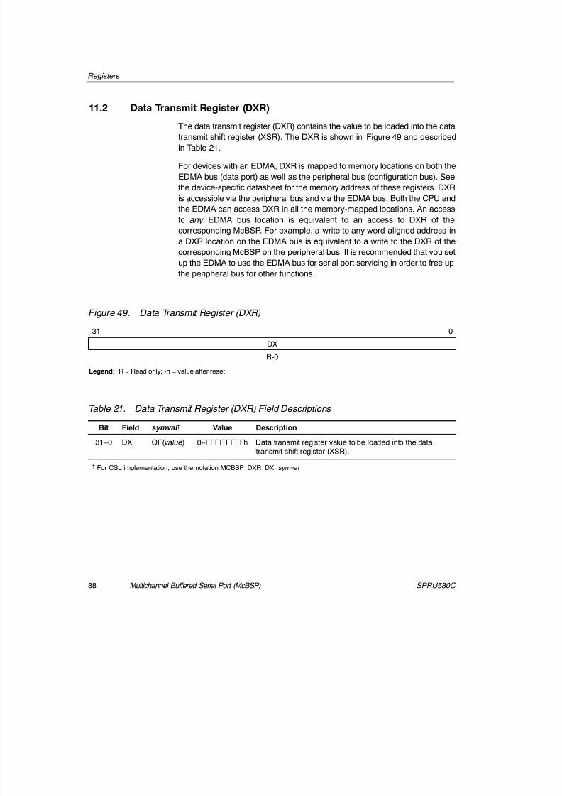
8/7/2019 McBSP Reference Guide- spru580c
http://slidepdf.com/reader/full/mcbsp-reference-guide-spru580c 88/120
Registers
Multichannel Buffered Serial Port (McBSP)88 SPRU580C
11.2 Data Transmit Register (DXR)
The data transmit register (DXR) contains the value to be loaded into the datatransmit shift register (XSR). The DXR is shown in Figure 49 and described
in Table 21.
For devices with an EDMA, DXR is mapped to memory locations on both the
EDMA bus (data port) as well as the peripheral bus (configuration bus). See
the device-specific datasheet for the memory address of these registers. DXR
is accessible via the peripheral bus and via the EDMA bus. Both the CPU and
the EDMA can access DXR in all the memory-mapped locations. An access
to any EDMA bus location is equivalent to an access to DXR of the
corresponding McBSP. For example, a write to any word-aligned address in
a DXR location on the EDMA bus is equivalent to a write to the DXR of the
corresponding McBSP on the peripheral bus. It is recommended that you setup the EDMA to use the EDMA bus for serial port servicing in order to free up
the peripheral bus for other functions.
Figure 49. Data Transmit Register (DXR)
31 0
DX
R-0
Legend: R = Read only; - n = value after reset
Table 21. Data Transmit Register (DXR) Field Descriptions
Bit Field symval † Value Description
31−0 DX OF(value) 0−FFFF FFFFh Data transmit register value to be loaded into the datatransmit shift register (XSR).
† For CSL implementation, use the notation MCBSP_DXR_DX_ symval

8/7/2019 McBSP Reference Guide- spru580c
http://slidepdf.com/reader/full/mcbsp-reference-guide-spru580c 89/120
Registers
89Multichannel Buffered Serial Port (McBSP)SPRU580C
11.3 Serial Port Control Register (SPCR)
The serial port is configured via the serial port control register (SPCR) and thepin control register (PCR). The SPCR contains McBSP status control bits. The
SPCR is shown in Figure 50 and described in Table 22.
Figure 50. Serial Port Control Register (SPCR)
31 26 25 24
Reserved FREE† SOFT†
R-0 R/W-0 R/W-0
23 22 21 20 19 18 17 16
FRST GRST XINTM XSYNCERR XEMPTY XRDY XRST
R/W-0 R/W-0 R/W-0 R/W-0 R-0 R-0 R/W-0
15 14 13 12 11 10 8
DLB RJUST CLKSTP Reserved
R/W-0 R/W-0 R/W-0 R-0
7 6 5 4 3 2 1 0
DXENA† Reserved RINTM RSYNCERR RFULL RRDY RRST
R/W-0 R-0 R/W-0 R/W-0 R-0 R-0 R/W-0† Available only on C621x/C671x DSP and C64x DSP.
Legend: R = Read only; R/W = Read/Write; - n = value after reset

8/7/2019 McBSP Reference Guide- spru580c
http://slidepdf.com/reader/full/mcbsp-reference-guide-spru580c 90/120
Registers
Multichannel Buffered Serial Port (McBSP)90 SPRU580C
Table 22. Serial Port Control Register (SPCR) Field Descriptions
Bit field † symval † Value Description
31−26 Reserved − 0 Reserved. The reserved bit location is always read as 0. Avalue written to this field has no effect.
25 FREE For C621x/C671x and C64x DSP: Free-running enablemode bit. This bit is used in conjunction with SOFT bit todetermine state of serial port clock during emulation halt.
NO 0 Free-running mode is disabled. During emulation halt, SOFTbit determines operation of McBSP.
YES 1 Free-running mode is enabled. During emulation halt, serialclocks continue to run.
24 SOFT For C621x/C671x and C64x DSP: Soft bit enable mode bit.This bit is used in conjunction with FREE bit to determinestate of serial port clock during emulation halt. This bit hasno effect if FREE = 1.
NO 0 Soft mode is disabled. Serial port clock stops immediatelyduring emulation halt, thus aborting any transmissions.
YES 1 Soft mode is enabled. During emulation halt, serial port clockstops after completion of current transmission.
23 FRST Frame-sync generator reset bit.
YES 0 Frame-synchronization logic is reset. Frame-sync signal
(FSG) is not generated by the sample-rate generator.
NO 1 Frame-sync signal (FSG) is generated after (FPER + 1)number of CLKG clocks; that is, all frame counters areloaded with their programmed values.
22 GRST Sample-rate generator reset bit.
YES 0 Sample-rate generator is reset.
NO 1 Sample-rate generator is taken out of reset. CLKG is drivenas per programmed value in sample-rate generator register(SRGR).
† For CSL implementation, use the notation MCBSP_SPCR_ field _ symval

8/7/2019 McBSP Reference Guide- spru580c
http://slidepdf.com/reader/full/mcbsp-reference-guide-spru580c 91/120
Registers
91Multichannel Buffered Serial Port (McBSP)SPRU580C
Table 22. Serial Port Control Register (SPCR) Field Descriptions (Continued)
Bit Description Valuesymval †field †
21−20 XINTM 0−3h Transmit interrupt (XINT) mode bit.
XRDY 0 XINT is driven by XRDY (end-of-word) and end-of-frame in
A-bis mode.
EOS 1h XINT is generated by end-of-block or end-of-frame inmultichannel operation.
FRM 2h XINT is generated by a new frame synchronization.
XSYNCERR 3h XINT is generated by XSYNCERR.
19 XSYNCERR Transmit synchronization error bit. Writing a 1 to XSYNCERR
sets the error condition when the transmitter is enabled(XRST = 1). Thus, it is used mainly for testing purposes or if this operation is desired.
NO 0 No synchronization error is detected.
YES 1 Synchronization error is detected.
18 XEMPTY Transmit shift register empty bit.
YES 0 XSR is empty.
NO 1 XSR is not empty.
17 XRDY Transmitter ready bit.
NO 0 Transmitter is not ready.
YES 1 Transmitter is ready for new data in DXR.
16 XRST Transmitter reset bit resets or enables the transmitter.
YES 0 Serial port transmitter is disabled and in reset state.
NO 1 Serial port transmitter is enabled.
15 DLB Digital loop back mode enable bit.
OFF 0 Digital loop back mode is disabled.
ON 1 Digital loop back mode is enabled.
† For CSL implementation, use the notation MCBSP_SPCR_ field _ symval

8/7/2019 McBSP Reference Guide- spru580c
http://slidepdf.com/reader/full/mcbsp-reference-guide-spru580c 92/120
Registers
Multichannel Buffered Serial Port (McBSP)92 SPRU580C
Table 22. Serial Port Control Register (SPCR) Field Descriptions (Continued)
Bit Description Valuesymval †field †
14−13 RJUST 0−3h Receive sign-extension and justification mode bit.
RZF 0 Right-justify and zero-fill MSBs in DRR.
RSE 1h Right-justify and sign-extend MSBs in DRR.
LZF 2h Left-justify and zero-fill LSBs in DRR.
− 3h Reserved
12−11 CLKSTP 0−3h Clock stop mode bit. In SPI mode, operates in conjunctionwith CLKXP bit of pin control register (PCR).
DISABLE 0−1h Clock stop mode is disabled. Normal clocking for non-SPI mode.
In SPI mode with data sampled on rising edge (CLKXP = 0):
NODELAY 2h Clock starts with rising edge without delay.
DELAY 3h Clock starts with rising edge with delay.
In SPI mode with data sampled on falling edge (CLKXP = 1):
NODELAY 2h Clock starts with falling edge without delay.
DELAY 3h Clock starts with falling edge with delay.
10−8 Reserved − 0 Reserved. The reserved bit location is always read as 0. Avalue written to this field has no effect.
7 DXENA For C621x/C671x and C64x DSP: DX enabler bit.
OFF 0 DX enabler is off.
ON 1 DX enabler is on.
6 Reserved − 0 Reserved. The reserved bit location is always read as 0. Avalue written to this field has no effect.
† For CSL implementation, use the notation MCBSP_SPCR_ field _ symval

8/7/2019 McBSP Reference Guide- spru580c
http://slidepdf.com/reader/full/mcbsp-reference-guide-spru580c 93/120
Registers
93Multichannel Buffered Serial Port (McBSP)SPRU580C
Table 22. Serial Port Control Register (SPCR) Field Descriptions (Continued)
Bit Description Valuesymval †field †
5−4 RINTM 0−3h Receive interrupt (RINT) mode bit.
RRDY 0 RINT is driven by RRDY (end-of-word) and end-of-frame in
A-bis mode.
EOS 1h RINT is generated by end-of-block or end-of-frame inmultichannel operation.
FRM 2h RINT is generated by a new frame synchronization.
RSYNCERR 3h RINT is generated by RSYNCERR.
3 RSYNCERR Receive synchronization error bit. Writing a 1 to RSYNCERR
sets the error condition when the receiver is enabled(RRST = 1). Thus, it is used mainly for testing purposes or if this operation is desired.
NO 0 No synchronization error is detected.
YES 1 Synchronization error is detected.
2 RFULL Receive shift register full bit.
NO 0 RBR is not in overrun condition.
YES 1 DRR is not read, RBR is full, and RSR is also full with newword.
1 RRDY Receiver ready bit.NO 0 Receiver is not ready.
YES 1 Receiver is ready with data to be read from DRR.
0 RRST Receiver reset bit resets or enables the receiver.
YES 0 The serial port receiver is disabled and in reset state.
NO 1 The serial port receiver is enabled.
† For CSL implementation, use the notation MCBSP_SPCR_ field _ symval

8/7/2019 McBSP Reference Guide- spru580c
http://slidepdf.com/reader/full/mcbsp-reference-guide-spru580c 94/120
Registers
Multichannel Buffered Serial Port (McBSP)94 SPRU580C
11.4 Receive Control Register (RCR)
The receive control register (RCR) configures parameters of the receive
operations. The RCR is shown in Figure 51 and described in Table 23.
Figure 51. Receive Control Register (RCR)
31 30 24 23 21 20 19 18 17 16
RPHASE RFRLEN2 RWDLEN2 RCOMPAND RFIG RDATDLY
R/W-0 R/W-0 R/W-0 R/W-0 R/W-0 R/W-0
15 14 8 7 5 4 3 0
Reserved RFRLEN1 RWDLEN1 RWDREVRS† Reserved
R-0 R/W-0 R/W-0 R/W-0 R-0
† Available only on C621x/C671x DSP and C64x DSP.
Legend: R = Read only; R/W = Read/Write; - n = value after reset
Table 23. Receive Control Register (RCR) Field Descriptions
Bit field † symval † Value Description
31 RPHASE Receive phases bit.
SINGLE 0 Single-phase frame
DUAL 1 Dual-phase frame
30−24 RFRLEN2 OF(value) 0−7Fh Specifies the receive frame length (number of words) in phase 2.
23−21 RWDLEN2 0−7h Specifies the receive word length (number of bits) in phase 2.
8BIT 0 Receive word length is 8 bits.
12BIT 1h Receive word length is 12 bits.
16BIT 2h Receive word length is 16 bits.
20BIT 3h Receive word length is 20 bits.
24BIT 4h Receive word length is 24 bits.
32BIT 5h Receive word length is 32 bits.
− 6h−7h Reserved
† For CSL implementation, use the notation MCBSP_RCR_ field _ symval

8/7/2019 McBSP Reference Guide- spru580c
http://slidepdf.com/reader/full/mcbsp-reference-guide-spru580c 95/120
Registers
95Multichannel Buffered Serial Port (McBSP)SPRU580C
Table 23. Receive Control Register (RCR) Field Descriptions (Continued)
Description Valuesymval †field †Bit
20−19 RCOMPAND 0−3h Receive companding mode bit. Modes other than 00 are onlyenabled when RWDLEN1/2 bit is 000 (indicating 8-bit data).
MSB 0 No companding, data transfer starts with MSB first.
8BITLSB 1h No companding, 8-bit data transfer starts with LSB first.
ULAW 2h Compand using µ-law for receive data.
ALAW 3h Compand using A-law for receive data.
18 RFIG Receive frame ignore bit.
NO 0 Receive frame-synchronization pulses after the first pulse
restarts the transfer.
YES 1 Receive frame-synchronization pulses after the first pulseare ignored.
17−16 RDATDLY 0−3h Receive data delay bit.
0BIT 0 0-bit data delay
1BIT 1h 1-bit data delay
2BIT 2h 2-bit data delay
− 3h Reserved
15 Reserved − 0 Reserved. The reserved bit location is always read as 0. A
value written to this field has no effect.
14−8 RFRLEN1 OF(value) 0−7Fh Specifies the receive frame length (number of words) in phase 1.
7−5 RWDLEN1 0−7h Specifies the receive word length (number of bits) in phase 1.
8BIT 0 Receive word length is 8 bits.
12BIT 1h Receive word length is 12 bits.
16BIT 2h Receive word length is 16 bits.
20BIT 3h Receive word length is 20 bits.
24BIT 4h Receive word length is 24 bits.
32BIT 5h Receive word length is 32 bits.
− 6h−7h Reserved
† For CSL implementation, use the notation MCBSP_RCR_ field _ symval

8/7/2019 McBSP Reference Guide- spru580c
http://slidepdf.com/reader/full/mcbsp-reference-guide-spru580c 96/120
Registers
Multichannel Buffered Serial Port (McBSP)96 SPRU580C
Table 23. Receive Control Register (RCR) Field Descriptions (Continued)
Description Valuesymval †field †Bit
4 RWDREVRS For C621x/C671x and C64x DSP: Receive 32-bit bit reversalenable bit.
DISABLE 0 32-bit bit reversal is disabled.
ENABLE 1 32-bit bit reversal is enabled. 32-bit data is received LSBfirst. RWDLEN1/2 bit should be set to 5h (32-bit operation);RCOMPAND bit should be set to 1h (transfer starts with LSBfirst); otherwise, operation is undefined.
3−0 Reserved − 0 Reserved. The reserved bit location is always read as 0. Avalue written to this field has no effect.
† For CSL implementation, use the notation MCBSP_RCR_ field _ symval

8/7/2019 McBSP Reference Guide- spru580c
http://slidepdf.com/reader/full/mcbsp-reference-guide-spru580c 97/120
Registers
97Multichannel Buffered Serial Port (McBSP)SPRU580C
11.5 Transmit Control Register (XCR)
The transmit control register (XCR) configures parameters of the transmitoperations. The XCR is shown in Figure 52 and described in Table 24.
Figure 52. Transmit Control Register (XCR)
31 30 24 23 21 20 19 18 17 16
XPHASE XFRLEN2 XWDLEN2 XCOMPAND XFIG XDATDLY
R/W-0 R/W-0 R/W-0 R/W-0 R/W-0 R/W-0
15 14 8 7 5 4 3 0
Reserved XFRLEN1 XWDLEN1 XWDREVRS† ReservedR-0 R/W-0 R/W-0 R/W-0 R-0
† Available only on C621x/C671x DSP and C64x DSP.
Legend: R = Read only; R/W = Read/Write; - n = value after reset
Table 24. Transmit Control Register (XCR) Field Descriptions
Bit field † symval † Value Description
31 XPHASE Transmit phases bit.
SINGLE 0 Single-phase frame
DUAL 1 Dual-phase frame
30−24 XFRLEN2 OF(value) 0−7Fh Specifies the transmit frame length (number of words) inphase 2.
23−21 XWDLEN2 0−7h Specifies the transmit word length (number of bits) in phase 2.
8BIT 0 Transmit word length is 8 bits.
12BIT 1h Transmit word length is 12 bits.
16BIT 2h Transmit word length is 16 bits.
20BIT 3h Transmit word length is 20 bits.
24BIT 4h Transmit word length is 24 bits.
32BIT 5h Transmit word length is 32 bits.
− 6h−7h Reserved
† For CSL implementation, use the notation MCBSP_XCR_ field _ symval
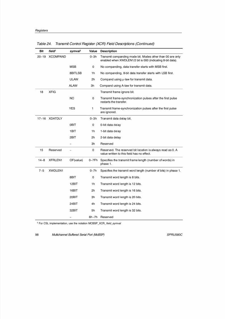
8/7/2019 McBSP Reference Guide- spru580c
http://slidepdf.com/reader/full/mcbsp-reference-guide-spru580c 98/120
Registers
Multichannel Buffered Serial Port (McBSP)98 SPRU580C
Table 24. Transmit Control Register (XCR) Field Descriptions (Continued)
Bit Description Valuesymval †field †
20−19 XCOMPAND 0−3h Transmit companding mode bit. Modes other than 00 are onlyenabled when XWDLEN1/2 bit is 000 (indicating 8-bit data).
MSB 0 No companding, data transfer starts with MSB first.
8BITLSB 1h No companding, 8-bit data transfer starts with LSB first.
ULAW 2h Compand using µ-law for transmit data.
ALAW 3h Compand using A-law for transmit data.
18 XFIG Transmit frame ignore bit.
NO 0 Transmit frame-synchronization pulses after the first pulse
restarts the transfer.
YES 1 Transmit frame-synchronization pulses after the first pulseare ignored.
17−16 XDATDLY 0−3h Transmit data delay bit.
0BIT 0 0-bit data delay
1BIT 1h 1-bit data delay
2BIT 2h 2-bit data delay
− 3h Reserved
15 Reserved − 0 Reserved. The reserved bit location is always read as 0. A
value written to this field has no effect.
14−8 XFRLEN1 OF(value) 0−7Fh Specifies the transmit frame length (number of words) inphase 1.
7−5 XWDLEN1 0−7h Specifies the transmit word length (number of bits) in phase 1.
8BIT 0 Transmit word length is 8 bits.
12BIT 1h Transmit word length is 12 bits.
16BIT 2h Transmit word length is 16 bits.
20BIT 3h Transmit word length is 20 bits.
24BIT 4h Transmit word length is 24 bits.
32BIT 5h Transmit word length is 32 bits.
− 6h−7h Reserved
† For CSL implementation, use the notation MCBSP_XCR_ field _ symval

8/7/2019 McBSP Reference Guide- spru580c
http://slidepdf.com/reader/full/mcbsp-reference-guide-spru580c 99/120
Registers
99Multichannel Buffered Serial Port (McBSP)SPRU580C
Table 24. Transmit Control Register (XCR) Field Descriptions (Continued)
Bit Description Valuesymval †field †
4 XWDREVRS For C621x/C671x and C64x DSP: Transmit 32-bit bit reversalfeature enable bit.
DISABLE 0 32-bit bit reversal is disabled.
ENABLE 1 32-bit bit reversal is enabled. 32-bit data is transmitted LSBfirst. XWDLEN1/2 bit should be set to 5h (32-bit operation);XCOMPAND bit should be set to 1h (transfer starts with LSBfirst); otherwise, operation is undefined.
3−0 Reserved − 0 Reserved. The reserved bit location is always read as 0. Avalue written to this field has no effect.
† For CSL implementation, use the notation MCBSP_XCR_ field _ symval
11.6 Sample Rate Generator Register (SRGR)
The sample rate generator register (SRGR) controls the operation of various
features of the sample rate generator. The SRGR is shown in Figure 53 and
described in Table 25.
Figure 53. Sample Rate Generator Register (SRGR)
31 30 29 28 27 16
GSYNC CLKSP CLKSM FSGM FPER
R/W-0 R/W-0 R/W-1 R/W-0 R/W-0
15 8 7 0
FWID CLKGDV
R/W-0 R/W-1
Legend: R/W = Read/Write; - n = value after reset
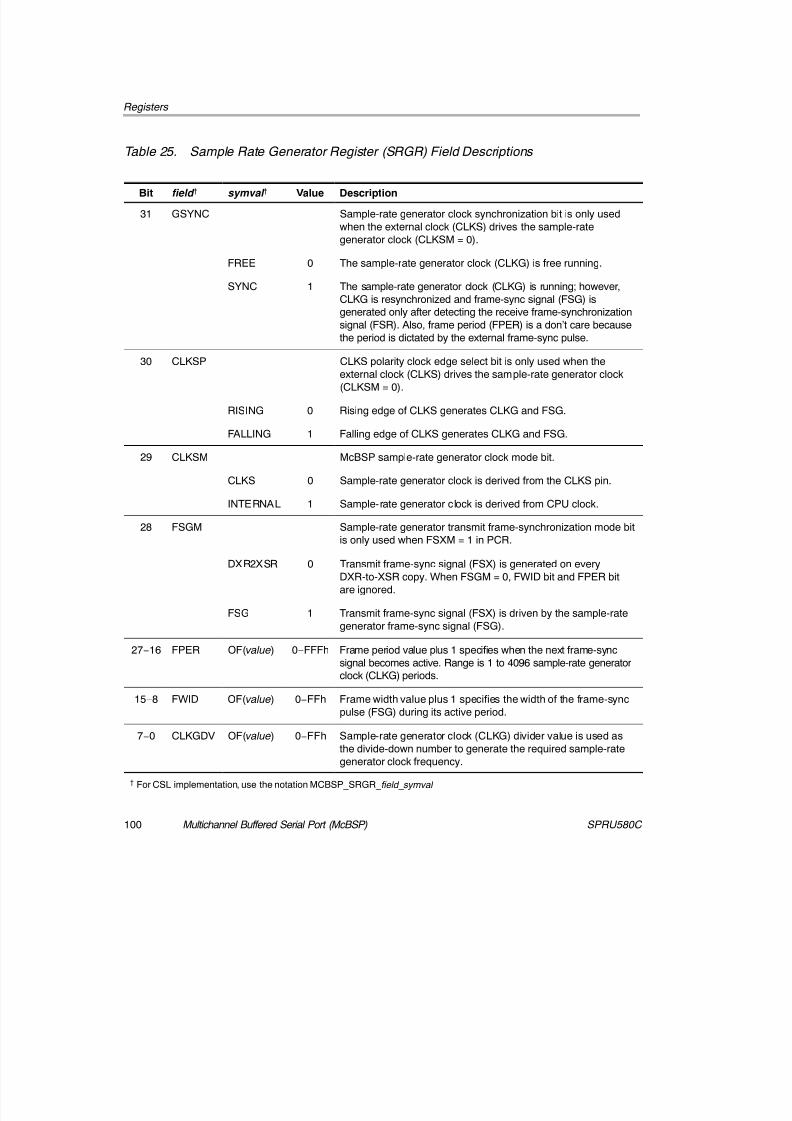
8/7/2019 McBSP Reference Guide- spru580c
http://slidepdf.com/reader/full/mcbsp-reference-guide-spru580c 100/120
Registers
Multichannel Buffered Serial Port (McBSP)100 SPRU580C
Table 25. Sample Rate Generator Register (SRGR) Field Descriptions
Bit field † symval † Value Description
31 GSYNC Sample-rate generator clock synchronization bit is only usedwhen the external clock (CLKS) drives the sample-rategenerator clock (CLKSM = 0).
FREE 0 The sample-rate generator clock (CLKG) is free running.
SYNC 1 The sample-rate generator clock (CLKG) is running; however,CLKG is resynchronized and frame-sync signal (FSG) isgenerated only after detecting the receive frame-synchronizationsignal (FSR). Also, frame period (FPER) is a don’t care becausethe period is dictated by the external frame-sync pulse.
30 CLKSP CLKS polarity clock edge select bit is only used when theexternal clock (CLKS) drives the sample-rate generator clock(CLKSM = 0).
RISING 0 Rising edge of CLKS generates CLKG and FSG.
FALLING 1 Falling edge of CLKS generates CLKG and FSG.
29 CLKSM McBSP sample-rate generator clock mode bit.
CLKS 0 Sample-rate generator clock is derived from the CLKS pin.
INTERNAL 1 Sample-rate generator clock is derived from CPU clock.
28 FSGM Sample-rate generator transmit frame-synchronization mode bit
is only used when FSXM = 1 in PCR.
DXR2XSR 0 Transmit frame-sync signal (FSX) is generated on everyDXR-to-XSR copy. When FSGM = 0, FWID bit and FPER bitare ignored.
FSG 1 Transmit frame-sync signal (FSX) is driven by the sample-rategenerator frame-sync signal (FSG).
27−16 FPER OF(value) 0−FFFh Frame period value plus 1 specifies when the next frame-syncsignal becomes active. Range is 1 to 4096 sample-rate generatorclock (CLKG) periods.
15−8 FWID OF(value) 0−FFh Frame width value plus 1 specifies the width of the frame-sync
pulse (FSG) during its active period.
7−0 CLKGDV OF(value) 0−FFh Sample-rate generator clock (CLKG) divider value is used asthe divide-down number to generate the required sample-rategenerator clock frequency.
† For CSL implementation, use the notation MCBSP_SRGR_ field _ symval
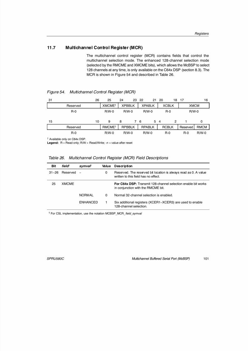
8/7/2019 McBSP Reference Guide- spru580c
http://slidepdf.com/reader/full/mcbsp-reference-guide-spru580c 101/120
Registers
101Multichannel Buffered Serial Port (McBSP)SPRU580C
11.7 Multichannel Control Register (MCR)
The multichannel control register (MCR) contains fields that control themultichannel selection mode. The enhanced 128-channel selection mode
(selected by the RMCME and XMCME bits), which allows the McBSP to select
128 channels at any time, is only available on the C64x DSP (section 8.3). The
MCR is shown in Figure 54 and described in Table 26.
Figure 54. Multichannel Control Register (MCR)
31 26 25 24 23 22 21 20 18 17 16
Reserved XMCME† XPBBLK XPABLK XCBLK XMCM
R-0 R/W-0 R/W-0 R/W-0 R-0 R/W-0
15 10 9 8 7 6 5 4 2 1 0
Reserved RMCME† RPBBLK RPABLK RCBLK Reserved RMCM
R-0 R/W-0 R/W-0 R/W-0 R-0 R-0 R/W-0
† Available only on C64x DSP.
Legend: R = Read only; R/W = Read/Write; - n = value after reset
Table 26. Multichannel Control Register (MCR) Field Descriptions
Bit field
†
symval
†
Value Description31−26 Reserved − 0 Reserved. The reserved bit location is always read as 0. A value
written to this field has no effect.
25 XMCME For C64x DSP: Transmit 128-channel selection enable bit worksin conjunction with the RMCME bit.
NORMAL 0 Normal 32-channel selection is enabled.
ENHANCED 1 Six additional registers (XCER1−XCER3) are used to enable128-channel selection.
† For CSL implementation, use the notation MCBSP_MCR_ field _ symval

8/7/2019 McBSP Reference Guide- spru580c
http://slidepdf.com/reader/full/mcbsp-reference-guide-spru580c 102/120
Registers
Multichannel Buffered Serial Port (McBSP)102 SPRU580C
Table 26. Multichannel Control Register (MCR) Field Descriptions (Continued)
Bit Description Valuesymval †field †
24−23 XPBBLK 0−3h Transmit partition B subframe bit. Enables 16 contiguous channelsin each subframe.
SF1 0 Subframe 1. Channel 16 to channel 31
SF3 1h Subframe 3. Channel 48 to channel 63
SF5 2h Subframe 5. Channel 80 to channel 95
SF7 3h Subframe 7. Channel 112 to channel 127
22−21 XPABLK 0−3h Transmit partition A subframe bit. Enables 16 contiguous channelsin each subframe.
SF0 0 Subframe 0. Channel 0 to channel 15
SF2 1h Subframe 2. Channel 32 to channel 47
SF4 2h Subframe 4. Channel 64 to channel 79
SF6 3h Subframe 6. Channel 96 to channel 111
20−18 XCBLK 0−7h Transmit current subframe bit.
SF0 0 Subframe 0. Channel 0 to channel 15
SF1 1h Subframe 1. Channel 16 to channel 31
SF2 2h Subframe 2. Channel 32 to channel 47
SF3 3h Subframe 3. Channel 48 to channel 63
SF4 4h Subframe 4. Channel 64 to channel 79
SF5 5h Subframe 5. Channel 80 to channel 95
SF6 6h Subframe 6. Channel 96 to channel 111
SF7 7h Subframe 7. Channel 112 to channel 127
† For CSL implementation, use the notation MCBSP_MCR_ field _ symval

8/7/2019 McBSP Reference Guide- spru580c
http://slidepdf.com/reader/full/mcbsp-reference-guide-spru580c 103/120
Registers
103Multichannel Buffered Serial Port (McBSP)SPRU580C
Table 26. Multichannel Control Register (MCR) Field Descriptions (Continued)
Bit Description Valuesymval †field †
17−16 XMCM 0−3h Transmit multichannel selection enable bit.
ENNOMASK 0 All channels are enabled without masking (DX is always driven
during transmission of data). DX is masked or driven to ahigh-impedance state during (a) interpacket intervals, (b) whena channel is masked regardless of whether it is enabled, or (c)when a channel is disabled.
DISXP 1h All channels are disabled and, therefore, masked by default.Required channels are selected by enabling XP[A/B]BLK andXCER[A/B] appropriately. Also, these selected channels are notmasked and, therefore, DX is always driven.
ENMASK 2h All channels are enabled, but masked. Selected channelsenabled using XP[A/B]BLK and XCER[A/B] are unmasked.
DISRP 3h All channels are disabled and, therefore, masked by default.Required channels are selected by enabling RP[A/B]BLK andRCER[A/B] appropriately. Selected channels can be unmasked byRP[A/B]BLK and XCER[A/B]. This mode is used for symmetrictransmit and receive operation.
15−10 Reserved − 0 Reserved. The reserved bit location is always read as 0. A valuewritten to this field has no effect.
9 RMCME For C64x DSP: Receive 128-channel selection enable bit works
in conjunction with the XMCME bit.
NORMAL 0 Normal 32-channel selection is enabled.
ENHANCED 1 Six additional registers (RCER1−RCER3) are used to enable128-channel selection.
8−7 RPBBLK 0−3h Receive partition B subframe bit. Enables 16 contiguous channelsin each subframe.
SF1 0 Subframe 1. Channel 16 to channel 31
SF3 1h Subframe 3. Channel 48 to channel 63
SF5 2h Subframe 5. Channel 80 to channel 95
SF7 3h Subframe 7. Channel 112 to channel 127
† For CSL implementation, use the notation MCBSP_MCR_ field _ symval

8/7/2019 McBSP Reference Guide- spru580c
http://slidepdf.com/reader/full/mcbsp-reference-guide-spru580c 104/120
Registers
Multichannel Buffered Serial Port (McBSP)104 SPRU580C
Table 26. Multichannel Control Register (MCR) Field Descriptions (Continued)
Bit Description Valuesymval †field †
6−5 RPABLK 0−3h Receive partition A subframe bit. Enables 16 contiguous channelsin each subframe.
SF0 0 Subframe 0. Channel 0 to channel 15
SF2 1h Subframe 2. Channel 32 to channel 47
SF4 2h Subframe 4. Channel 64 to channel 79
SF6 3h Subframe 6. Channel 96 to channel 111
4−2 RCBLK 0−7h Receive current subframe bit.
SF0 0 Subframe 0. Channel 0 to channel 15
SF1 1h Subframe 1. Channel 16 to channel 31
SF2 2h Subframe 2. Channel 32 to channel 47
SF3 3h Subframe 3. Channel 48 to channel 63
SF4 4h Subframe 4. Channel 64 to channel 79
SF5 5h Subframe 5. Channel 80 to channel 95
SF6 6h Subframe 6. Channel 96 to channel 111
SF7 7h Subframe 7. Channel 112 to channel 127
1 Reserved−
0 Reserved. The reserved bit location is always read as 0. A valuewritten to this field has no effect.
0 RMCM Receive multichannel selection enable bit.
CHENABLE 0 All 128 channels are enabled.
ELDISABLE 1 All channels are disabled by default. Required channels areselected by enabling RP[A/B]BLK and RCER[A/B] appropriately.
† For CSL implementation, use the notation MCBSP_MCR_ field _ symval
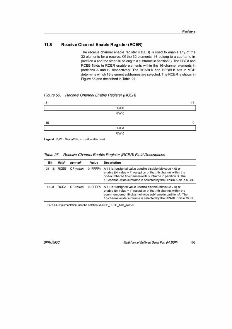
8/7/2019 McBSP Reference Guide- spru580c
http://slidepdf.com/reader/full/mcbsp-reference-guide-spru580c 105/120
Registers
105Multichannel Buffered Serial Port (McBSP)SPRU580C
11.8 Receive Channel Enable Register (RCER)
The receive channel enable register (RCER) is used to enable any of the32 elements for a receive. Of the 32 elements, 16 belong to a subframe in
partition A and the other 16 belong to a subframe in partition B. The RCEA and
RCEB fields in RCER enable elements within the 16-channel elements in
partitions A and B, respectively. The RPABLK and RPBBLK bits in MCR
determine which 16-element subframes are selected. The RCER is shown in
Figure 55 and described in Table 27.
Figure 55. Receive Channel Enable Register (RCER)
31 16
RCEB
R/W-0
15 0
RCEA
R/W-0
Legend: R/W = Read/Write; - n = value after reset
Table 27. Receive Channel Enable Register (RCER) Field Descriptions
Bit field † symval † Value Description
31−16 RCEB OF(value) 0−FFFFh A 16-bit unsigned value used to disable (bit value = 0) orenable (bit value = 1) reception of the nth channel within theodd-numbered 16-channel-wide subframe in partition B. The16-channel-wide subframe is selected by the RPBBLK bit in MCR.
15−0 RCEA OF(value) 0−FFFFh A 16-bit unsigned value used to disable (bit value = 0) orenable (bit value = 1) reception of the nth channel within theeven-numbered 16-channel-wide subframe in partition A. The16-channel-wide subframe is selected by the RPABLK bit in MCR.
† For CSL implementation, use the notation MCBSP_RCER_ field _ symval

8/7/2019 McBSP Reference Guide- spru580c
http://slidepdf.com/reader/full/mcbsp-reference-guide-spru580c 106/120
Registers
Multichannel Buffered Serial Port (McBSP)106 SPRU580C
11.9 Transmit Channel Enable Registers (XCER)
The transmit channel enable register (XCER) is used to enable any of the32 elements for a transmit. Of the 32 elements, 16 belong to a subframe in
partition A and the other 16 belong to a subframe in partition B. The XCEA and
XCEB fields in XCER enable elements within the 16-channel elements in
partitions A and B, respectively. The XPABLK and XPBBLK bits in MCR
determine which 16-element subframes are selected. The XCER is shown in
Figure 56 and described in Table 28.
Figure 56. Transmit Channel Enable Register (XCER)
31 16
XCEB
R/W-0
15 0
XCEA
R/W-0
Legend: R/W = Read/Write; - n = value after reset
Table 28. Transmit Channel Enable Register (XCER) Field Descriptions
Bit field † symval † Value Description
31−16 XCEB OF(value) 0−FFFFh A 16-bit unsigned value used to disable (bit value = 0) orenable (bit value = 1) transmission of the nth channel within theodd-numbered 16-channel-wide subframe in partition B. The16-channel-wide subframe is selected by the XPBBLK bit in MCR.
15−0 XCEA OF(value) 0−FFFFh A 16-bit unsigned value used to disable (bit value = 0) orenable (bit value = 1) transmission of the nth channel within theeven-numbered 16-channel-wide subframe in partition A. The16-channel-wide subframe is selected by the XPABLK bit in MCR.
† For CSL implementation, use the notation MCBSP_XCER_ field _ symval
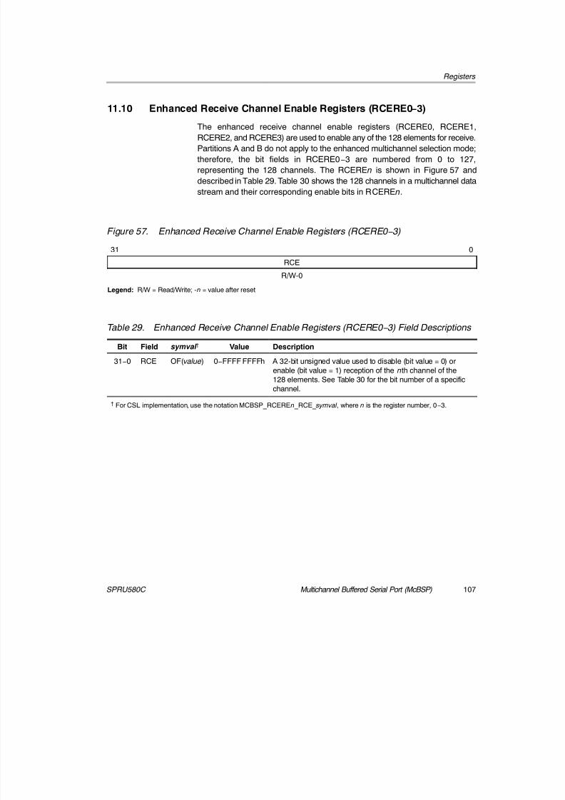
8/7/2019 McBSP Reference Guide- spru580c
http://slidepdf.com/reader/full/mcbsp-reference-guide-spru580c 107/120
Registers
107Multichannel Buffered Serial Port (McBSP)SPRU580C
11.10 Enhanced Receive Channel Enable Registers (RCERE0−3)
The enhanced receive channel enable registers (RCERE0, RCERE1,RCERE2, and RCERE3) are used to enable any of the 128 elements for receive.
Partitions A and B do not apply to the enhanced multichannel selection mode;
therefore, the bit fields in RCERE0−3 are numbered from 0 to 127,
representing the 128 channels. The RCERE n is shown in Figure 57 and
described in Table 29. Table 30 shows the 128 channels in a multichannel data
stream and their corresponding enable bits in RCERE n.
Figure 57. Enhanced Receive Channel Enable Registers (RCERE0− 3)
31 0
RCE
R/W-0
Legend: R/W = Read/Write; - n = value after reset
Table 29. Enhanced Receive Channel Enable Registers (RCERE0− 3) Field Descriptions
Bit Field symval † Value Description
31−0 RCE OF(value) 0−FFFF FFFFh A 32-bit unsigned value used to disable (bit value = 0) orenable (bit value = 1) reception of the nth channel of the
128 elements. See Table 30 for the bit number of a specificchannel.
† For CSL implementation, use the notation MCBSP_RCERE n _RCE_ symval , where n is the register number, 0−3.

8/7/2019 McBSP Reference Guide- spru580c
http://slidepdf.com/reader/full/mcbsp-reference-guide-spru580c 108/120
Registers
Multichannel Buffered Serial Port (McBSP)108 SPRU580C
Table 30. Channel Enable Bits in RCERE n for a 128-Channel Data Stream
Channel Number of a 128-Channel Data Stream (RCEn )
RCEREn
Bit 0 - 15 16 - 31 32 - 47 48 - 63 64 - 79 80 - 95 96 - 111 112-127
0 RCERE0 RCERE1 RCERE2 RCERE3
1 RCERE0 RCERE1 RCERE2 RCERE3
2 RCERE0 RCERE1 RCERE2 RCERE3
3 RCERE0 RCERE1 RCERE2 RCERE3
4 RCERE0 RCERE1 RCERE2 RCERE3
5 RCERE0 RCERE1 RCERE2 RCERE3
6 RCERE0 RCERE1 RCERE2 RCERE3
7 RCERE0 RCERE1 RCERE2 RCERE3
8 RCERE0 RCERE1 RCERE2 RCERE3
9 RCERE0 RCERE1 RCERE2 RCERE3
10 RCERE0 RCERE1 RCERE2 RCERE3
11 RCERE0 RCERE1 RCERE2 RCERE3
12 RCERE0 RCERE1 RCERE2 RCERE3
13 RCERE0 RCERE1 RCERE2 RCERE3
14 RCERE0 RCERE1 RCERE2 RCERE3
15 RCERE0 RCERE1 RCERE2 RCERE3
16 RCERE0 RCERE1 RCERE2 RCERE3
17 RCERE0 RCERE1 RCERE2 RCERE3
18 RCERE0 RCERE1 RCERE2 RCERE319 RCERE0 RCERE1 RCERE2 RCERE3
20 RCERE0 RCERE1 RCERE2 RCERE3
21 RCERE0 RCERE1 RCERE2 RCERE3
22 RCERE0 RCERE1 RCERE2 RCERE3
23 RCERE0 RCERE1 RCERE2 RCERE3
24 RCERE0 RCERE1 RCERE2 RCERE3
25 RCERE0 RCERE1 RCERE2 RCERE3
26 RCERE0 RCERE1 RCERE2 RCERE3
27 RCERE0 RCERE1 RCERE2 RCERE3
28 RCERE0 RCERE1 RCERE2 RCERE3
29 RCERE0 RCERE1 RCERE2 RCERE3
30 RCERE0 RCERE1 RCERE2 RCERE3
31 RCERE0 RCERE1 RCERE2 RCERE3

8/7/2019 McBSP Reference Guide- spru580c
http://slidepdf.com/reader/full/mcbsp-reference-guide-spru580c 109/120
Registers
109Multichannel Buffered Serial Port (McBSP)SPRU580C
11.11 Enhanced Transmit Channel Enable Registers (XCERE0−3)
The enhanced transmit channel enable registers (XCERE0, XCERE1,XCERE2, and XCERE3) are used to enable any of the 128 elements for transmit.
Partitions A and B do not apply to the enhanced multichannel selection mode;
therefore, the bit fields in XCERE0−3 are numbered from 0 to 127,
representing the 128 channels. The XCERE n is shown in Figure 58 and
described in Table 31. Table 32 shows the 128 channels in a multichannel data
stream and their corresponding enable bits in XCERE n.
Figure 58. Enhanced Transmit Channel Enable Registers (XCERE0− 3)
31 0
XCE
R/W-0
Legend: R/W = Read/Write; - n = value after reset
Table 31. Enhanced Transmit Channel Enable Registers (XCERE0− 3) Field Descriptions
Bit Field symval † Value Description
31−0 XCE OF(value) 0−FFFF FFFFh A 32-bit unsigned value used to disable (bit value = 0) orenable (bit value = 1) transmission of the nth channel of the
128 elements. See Table 32 for the bit number of a specificchannel.
† For CSL implementation, use the notation MCBSP_XCERE n _XCE_ symval , where n is the register number, 0−3.

8/7/2019 McBSP Reference Guide- spru580c
http://slidepdf.com/reader/full/mcbsp-reference-guide-spru580c 110/120
Registers
Multichannel Buffered Serial Port (McBSP)110 SPRU580C
Table 32. Channel Enable Bits in XCERE n for a 128-Channel Data Stream
Channel Number of a 128-Channel Data Stream (XCEn )
XCEREn
Bit 0 - 15 16 - 31 32 - 47 48 - 63 64 - 79 80 - 95 96 - 111 112-127
0 XCERE0 XCERE1 XCERE2 XCERE3
1 XCERE0 XCERE1 XCERE2 XCERE3
2 XCERE0 XCERE1 XCERE2 XCERE3
3 XCERE0 XCERE1 XCERE2 XCERE3
4 XCERE0 XCERE1 XCERE2 XCERE3
5 XCERE0 XCERE1 XCERE2 XCERE3
6 XCERE0 XCERE1 XCERE2 XCERE3
7 XCERE0 XCERE1 XCERE2 XCERE3
8 XCERE0 XCERE1 XCERE2 XCERE3
9 XCERE0 XCERE1 XCERE2 XCERE3
10 XCERE0 XCERE1 XCERE2 XCERE3
11 XCERE0 XCERE1 XCERE2 XCERE3
12 XCERE0 XCERE1 XCERE2 XCERE3
13 XCERE0 XCERE1 XCERE2 XCERE3
14 XCERE0 XCERE1 XCERE2 XCERE3
15 XCERE0 XCERE1 XCERE2 XCERE3
16 XCERE0 XCERE1 XCERE2 XCERE3
17 XCERE0 XCERE1 XCERE2 XCERE3
18 XCERE0 XCERE1 XCERE2 XCERE319 XCERE0 XCERE1 XCERE2 XCERE3
20 XCERE0 XCERE1 XCERE2 XCERE3
21 XCERE0 XCERE1 XCERE2 XCERE3
22 XCERE0 XCERE1 XCERE2 XCERE3
23 XCERE0 XCERE1 XCERE2 XCERE3
24 XCERE0 XCERE1 XCERE2 XCERE3
25 XCERE0 XCERE1 XCERE2 XCERE3
26 XCERE0 XCERE1 XCERE2 XCERE3
27 XCERE0 XCERE1 XCERE2 XCERE3
28 XCERE0 XCERE1 XCERE2 XCERE3
29 XCERE0 XCERE1 XCERE2 XCERE3
30 XCERE0 XCERE1 XCERE2 XCERE3
31 XCERE0 XCERE1 XCERE2 XCERE3

8/7/2019 McBSP Reference Guide- spru580c
http://slidepdf.com/reader/full/mcbsp-reference-guide-spru580c 111/120
Registers
111Multichannel Buffered Serial Port (McBSP)SPRU580C
11.12 Pin Control Register (PCR)
The serial port is configured via the serial port control register (SPCR) and thepin control register (PCR). The PCR is also used to configure the serial port
pins as general-purpose inputs or outputs during receiver and/or transmitter
reset (for more information see section 10). The PCR contains McBSP status
control bits. The PCR is shown in Figure 59 and described in Table 33.
Figure 59. Pin Control Register (PCR)
31 16
Reserved
R-0
15 14 13 12 11 10 9 8
Reserved XIOEN RIOEN FSXM FSRM CLKXM CLKRM
R-0 R/W-0 R/W-0 R/W-0 R/W-0 R/W-0 R/W-0
7 6 5 4 3 2 1 0
Reserved† CLKSSTAT DXSTAT DRSTAT FSXP FSRP CLKXP CLKRP
R-0 R-0 R/W-0 R-0 R/W-0 R/W-0 R/W-0 R/W-0
Legend: R = Read only; R/W = Read/Write; - n = value after reset† If writing to this field, always write the default value of 0 to ensure proper McBSP operation.
Table 33. Pin Control Register (PCR) Field Descriptions
Bit field † symval † Value Description
31−14 Reserved − 0 Reserved. The reserved bit location is always read as 0. Avalue written to this field has no effect.
13 XIOEN Transmit general-purpose I/O mode only when transmitter isdisabled (XRST = 0 in SPCR).
SP 0 DX, FSX, and CLKX pins are configured as serial port pins
and do not function as general-purpose I/O pins.
GPIO 1 DX pin is configured as general-purpose output pin; FSX
and CLKX pins are configured as general-purpose I/O pins.These serial port pins do not perform serial port operations.
† For CSL implementation, use the notation MCBSP_PCR_ field _ symval

8/7/2019 McBSP Reference Guide- spru580c
http://slidepdf.com/reader/full/mcbsp-reference-guide-spru580c 112/120
Registers
Multichannel Buffered Serial Port (McBSP)112 SPRU580C
Table 33. Pin Control Register (PCR) Field Descriptions (Continued)
Description Valuesymval †field †Bit
12 RIOEN Receive general-purpose I/O mode only when receiver isdisabled (RRST = 0 in SPCR).
SP 0 DR, FSR, CLKR, and CLKS pins are configured as serialport pins and do not function as general-purpose I/O pins.
GPIO 1 DR and CLKS pins are configured as general-purpose inputpins; FSR and CLKR pins are configured asgeneral-purpose I/O pins. These serial port pins do not
perform serial port operations.
11 FSXM Transmit frame-synchronization mode bit.
EXTERNAL 0 Frame-synchronization signal is derived from an externalsource.
INTERNAL 1 Frame-synchronization signal is determined by FSGM bit inSRGR.
10 FSRM Receive frame-synchronization mode bit.
EXTERNAL 0 Frame-synchronization signal is derived from an externalsource. FSR is an input pin.
INTERNAL 1 Frame-synchronization signal is generated internally by thesample-rate generator. FSR is an output pin, except whenGSYNC = 1 in SRGR.
9 CLKXM Transmitter clock mode bit.
INPUT 0 CLKX is an input pin and is driven by an external clock.
OUTPUT 1 CLKX is an output pin and is driven by the internalsample-rate generator.
In SPI mode when CLKSTP in SPCR is a non-zero value:
INPUT 0 MCBSP is a slave and clock (CLKX) is driven by the SPImaster in the system. CLKR is internally driven by CLKX.
OUTPUT 1 MCBSP is a master and generates the clock (CLKX) todrive its receive clock (CLKR) and the shift clock of theSPI-compliant slaves in the system.
† For CSL implementation, use the notation MCBSP_PCR_ field _ symval
8/7/2019 McBSP Reference Guide- spru580c
http://slidepdf.com/reader/full/mcbsp-reference-guide-spru580c 113/120
Registers
113Multichannel Buffered Serial Port (McBSP)SPRU580C
Table 33. Pin Control Register (PCR) Field Descriptions (Continued)
Description Valuesymval †field †Bit
8 CLKRM Receiver clock mode bit.
Digital loop back mode is disabled (DLB = 0 in SPCR):
INPUT 0 CLKR is an input pin and is driven by an external clock.
OUTPUT 1 CLKR is an output pin and is driven by the internal
sample-rate generator.
Digital loop back mode is enabled (DLB = 1 in SPCR):
INPUT 0 Receive clock (not the CLKR pin) is driven by transmit clock(CLKX) that is based on CLKXM bit. CLKR pin is in
high-impedance state.
OUTPUT 1 CLKR is an output pin and is driven by the transmit clock.The transmit clock is based on CLKXM bit.
7 Reserved − 0 Reserved. The reserved bit location is always read as 0. Avalue written to this field has no effect. If writing to this field,always write the default value of 0 to ensure proper McBSPoperation.
6 CLKSSTAT CLKS pin status reflects value on CLKS pin whenconfigured as a general-purpose input pin.
0 0 CLKS pin reflects a logic low.
1 1 CLKS pin reflects a logic high.
5 DXSTAT DX pin status reflects value driven to DX pin whenconfigured as a general-purpose output pin.
0 0 DX pin reflects a logic low.
1 1 DX pin reflects a logic high.
4 DRSTAT DR pin status reflects value on DR pin when configured as ageneral-purpose input pin.
0 0 DR pin reflects a logic low.
1 1 DR pin reflects a logic high.
† For CSL implementation, use the notation MCBSP_PCR_ field _ symval

8/7/2019 McBSP Reference Guide- spru580c
http://slidepdf.com/reader/full/mcbsp-reference-guide-spru580c 114/120
Registers
Multichannel Buffered Serial Port (McBSP)114 SPRU580C
Table 33. Pin Control Register (PCR) Field Descriptions (Continued)
Description Valuesymval †field †Bit
3 FSXP Transmit frame-synchronization polarity bit.
ACTIVEHIGH 0 Transmit frame-synchronization pulse is active high.
ACTIVELOW 1 Transmit frame-synchronization pulse is active low.
2 FSRP Receive frame-synchronization polarity bit.
ACTIVEHIGH 0 Receive frame-synchronization pulse is active high.
ACTIVELOW 1 Receive frame-synchronization pulse is active low.
1 CLKXP Transmit clock polarity bit.
RISING 0 Transmit data sampled on rising edge of CLKX.
FALLING 1 Transmit data sampled on falling edge of CLKX.
0 CLKRP Receive clock polarity bit.
FALLING 0 Receive data sampled on falling edge of CLKR.
RISING 1 Receive data sampled on rising edge of CLKR.
† For CSL implementation, use the notation MCBSP_PCR_ field _ symval

8/7/2019 McBSP Reference Guide- spru580c
http://slidepdf.com/reader/full/mcbsp-reference-guide-spru580c 115/120
115Multichannel Buffered Serial Port (McBSP)SPRU580C
Revision History
Table 34 lists the changes made since the previous version of this document.
Table 34. Document Revision History
Page Additions/Modifications/Deletions
14 Added new sentences after third sentence in first paragraph: Non-32-bit write accesses to controlregisters can result in corrupting the control register value. This is because undefined values arewritten to non-enabled bytes. However, non-32-bit read accesses return the correct value.
18 In section 3.4, changed last sentence to: The configuration is independent for receive and transmit.
38 In section 4.5.7, changed last sentence to: If the (R/W)WDREVRS and (R/X)COMPAND fields areset as indicated above, but the element size is not set to 32-bit, operation is undefined.

8/7/2019 McBSP Reference Guide- spru580c
http://slidepdf.com/reader/full/mcbsp-reference-guide-spru580c 116/120
Multichannel Buffered Serial Port (McBSP)116 SPRU580C
This page is intentionally left blank.

8/7/2019 McBSP Reference Guide- spru580c
http://slidepdf.com/reader/full/mcbsp-reference-guide-spru580c 117/120
Index
117Multichannel Buffered Serial Port (McBSP)SPRU580C
Index
32-bit bit reversal (RWDREVRS, XWDREVRS) 38
Bbit clock polarity (CLKSP) 24
bit ordering 61
block diagramclock and frame generation 19companding of internal data 61McBSP 13sample rate generator 22SPI configuration
McBSP as master 77
McBSP as slave 77
Cchanging element selection 73
CLKGDV bits 99
CLKRM bit 111
CLKRP bit 111
CLKSM bit 99
CLKSP bit 99
CLKSSTAT bit 111
CLKSTP bits 89
CLKXM bit 111
CLKXP bit 111
clock configuration 18, 32
clock operation 20
clocking examples 38double-rate clock 42double-rate ST-BUS clock 40single-rate ST-BUS clock 41
companding data format 60
companding hardware 59
companding internal data 60
configurationelement length 34
frame and clock 18, 32frame length 33
CPU interrupts 18
Ddata clock generation 23
bit clock 25frame synchronization 25receive clock selection 27transmit clock selection 27
data delay 36
data packing 34
data packing using frame sync ignore bits 49data receive register (DRR) 87
data reception 15
data transmission 15
data transmit register (DXR) 88
determining ready status 17
digital loopback mode (DLB) 26
DLB bit 89
DR bits 87
DRR 87
DRSTAT bit 111
DX bits 88
DXENA bit 89DXR 88
DXSTAT bit 111

8/7/2019 McBSP Reference Guide- spru580c
http://slidepdf.com/reader/full/mcbsp-reference-guide-spru580c 118/120
Index
118 Multichannel Buffered Serial Port (McBSP) SPRU580C
Eelement length 34
end-of-frame interrupt 73
enhanced multichannel selection mode(C64x DSP only) 73
enhanced receive channel enable register(RCERE) 107
enhanced transmit channel enable register(XCERE) 109
exception conditions 50
F
features 11FPER bits 99
frame configuration 18, 32
frame frequency 46
frame length 33
frame operation 20
frame sync signal generation 28frame detection for initialization 31frame period (FPER) 29frame width (FWID) 29receive frame sync signal selection 30
transmit frame sync signal selection 31
frame synchronization ignore 47
frame synchronization phases 32FREE bit 89
FRST bit 89
FSGM bit 99
FSRM bit 111
FSRP bit 111
FSXM bit 111
FSXP bit 111
FWID bits 99
G
GRST bit 89GSYNC bit 99
I
ignore frame synchronization 47
initialization procedure 62
input clock source mode (CLKSM) 23
interface signals 13
interrupts CPU 18
M
maximum frame frequency 46
McBSP initialization for SPI mode 81
McBSP operationas SPI master 80as SPI slave 81standard 43
MCR 101
multichannel control register (MCR) 101
multichannel selection operation 68DX enabler (DXENA) 75changing element selection 73enabling and masking of channels 69end-of-block interrupt 73enhanced multichannel selection mode
(C64x DSP only) 73
multichannel enable 69multiphase frame example 38
N
notational conventions 3
O
operationMcBSP standard 43
receive 44transmit 45

8/7/2019 McBSP Reference Guide- spru580c
http://slidepdf.com/reader/full/mcbsp-reference-guide-spru580c 119/120
Index
119Multichannel Buffered Serial Port (McBSP)SPRU580C
PPCR 111
pin control register (PCR) 111
pins as general-purpose I/O 83
programmable clock 19
programmable clock and framingdouble-rate clock example 42double-rate ST-BUS clock example 40examples 38single-rate ST-BUS clock example 41
programmable framing 19
RRCBLK bits 101
RCE bits 107
RCEA bits 105
RCEB bits 105
RCER 105
RCERE 107
RCOMPAND bits 94
RCR 94
RDATDLY bits 94
ready status 17
receive channel enable register (RCER) 105receive control register (RCR) 94
receive data justification (RJUST) 37
receive interrupt (RINT) 18
receive operation 44
receive overrun (RFULL) 50
receive ready status 17
reception, data 15
registers 84data receive register (DRR) 87data transmit register (DXR) 88enhanced receive channel enable register
(RCERE) 107enhanced transmit channel enable register
(XCERE) 109multichannel control register (MCR) 101pin control register (PCR) 111receive channel enable register (RCER) 105receive control register (RCR) 94
sample rate generator register (SRGR) 99serial port control register (SPCR) 89
transmit channel enable register (XCER) 106transmit control register (XCR) 97
related documentation from Texas Instruments 3
reset serial port 15
revision history 115
RFIG bit 94
RFRLEN1 bits 94
RFRLEN2 bits 94
RFULL bit 89
RINTM bits 89
RIOEN bit 111
RJUST bits 89
RMCM bit 101RMCME bit 101
RPABLK bits 101
RPBBLK bits 101
RPHASE bit 94
RRDY bit 89
RRST bit 89
RSYNCERR bit 89
RWDLEN1 bits 94
RWDLEN2 bits 94
RWDREVRS bit 94
Ssample rate generator
block diagram 22clocking and framing 22
sample rate generator data bit clock rate(CLKGDV) 23
sample rate generator register (SRGR) 99
serial port, reset 15
serial port control register (SPCR) 89
serial port exception conditions 50
signals 13
SOFT bit 89SPCR 89
SPI protocol (CLKSTP) 77
SRGR 99
standard operation 43
stopping clocks 28

8/7/2019 McBSP Reference Guide- spru580c
http://slidepdf.com/reader/full/mcbsp-reference-guide-spru580c 120/120
Index
Ttrademarks 4
transmission, data 15
transmit channel enable register (XCER) 106
transmit control register (XCR) 97
transmit data companding format 60
transmit empty (XEMPTY) 55
transmit interrupt (XINT) 18
transmit operation 45
transmit ready status 17
transmit with data overwrite 54
Uunexpected frame sync pulses 47
unexpected receive frame synchronization(RSYNCERR) 52
unexpected transmit frame synchronization(XSYNCERR) 56
X XCBLK bits 101
XCE bits 109
XCEA bits 106
XCEB bits 106
XCER 106
XCERE 109
XCOMPAND bits 97
XCR 97
XDATDLY bits 97
XEMPTY bit 89
XFIG bit 97
XFRLEN1 bits 97
XFRLEN2 bits 97
XINTM bits 89
XIOEN bit 111
XMCM bits 101
XMCME bit 101
XPABLK bits 101
XPBBLK bits 101
XPHASE bit 97
XRDY bit 89
XRST bit 89
XSYNCERR bit 89
XWDLEN1 bits 97
XWDLEN2 bits 97
XWDREVRS bit 97