mc93f5508b manualabov.co.kr/data/manual/um_mc93f5516_v2.03_en.pdf · · 2014-04-02mc93f5516 april...
TRANSCRIPT
MC93F5516
April 1, 2014 Ver. 2.0.3 1
ABOV SEMICONDUCTOR Co., Ltd.
LED Back Light Unit
MC93F5516
User’s Manual
(Ver.2.0.3 )
Published by ABOV
2013 ABOV Semiconductor Co., Ltd. All rights reserved.
Additional information of this manual may be served by ABOV Semiconductor offices in Korea or Distributors.
ABOV Semiconductor reserves the right to make changes to any information here in at any time without notice.
The information, diagrams and other data in this manual are correct and reliable; however, ABOV Semiconductor is in no
way responsible for any violations of patents or other rights of the third party generated by the use of this manual.
MC93F5516
2 April 1, 2014 Ver. 2.0.3
MC93F5516
CMOS SINGLE-CHIP 8-BIT MICROCONTROLLER
FOR LED BLU CONTROLLER
1. Overview
1.1 Description
The MC93F5516 is advanced CMOS 8-bit microcontroller with 16K bytes of FLASH. This is powerful
microcontroller which provides a higly flesible and cost effective solution to many embedded control
applications. And the MC93F5516 contains high performance M8051 core and DSP.
This provides the following features.
Device CPU FLASH XRAM IRAM Comm. DAC ADC Peri. for LED BLU
MC93F5516
M8051
+
DSP
16KB
3KB
-
256
bytes
256
bytes
I2C : 1ch
SPI : 2ch
(Master : 1,
Salve : 1)
2ch 3ch
SYNC Processor
PWM Detector
6ch PWM Output
Calculator
1.2 Features
• CPU : M8051(8051 Compatible) + DSP
• 16K bytes On-chip Flash
- Endurance : 1,000 times
- Retention : 10 years
• 256 bytes SRAM, 3KB-256 bytes XRAM
• General Purpose I/O : 22 ports
• WDT(Watch Dog Timer) : 8-bit x 1
• Timer/Counter : 2ch
- 16-bit Timer/Counter : T0
- 8-bit Timer/Counter : T1
• Capture Counter : 20-bit x 1ch
• High Frequency PWM : 12-bit x 6ch
• Serial Peripheral Interface(SPI) : 2ch
- Slave : 1ch, RX DMA Available
- Master : 1ch, TX DMA Available
• I2C : 1ch
• 8-bit ADC : 3 ch
• SYNC Processor
- VSYNC_I : 20-bit
- HSYNC : 24-bit
• Calculatord
- Local Dimming Calculation
• Internal OSC : 20 MHz (±2%)
• Vectored Interrupt Controller :11 Sources
• On-Chip POR(Power On Reset) : 2.2 V
• Operating Frequency
: 0.15625MHz ~ 20MHz
• Operating Voltage : 3.0 ~ 3.6 V
• Operating Temperature : -40 ~ +85
• Package Type : 24 QFN, 24 SSOP
MC93F5516
April 1, 2014 Ver. 2.0.3 3
1.3 Ordering Information
Device name ROM size IRAM size XRAM Package
MC93F5516UB 16KB FLASH 256 bytes 3KB – 256 bytes
24 QFN
MC93F5516SB 24 SSOP
Table 1.1 Order Inforrmation
1.4 Development Tools
1.4.1 Compiler
ABOV semiconductor does not provide any compiler for the MC93F5516. But the CPU core of
MC93F5516 is Mentor 8051, you can use all kinds of third party’s standard 8051 compiler like Keil C
Compiler, Open Source SDCC (Small Device C Compiler). These compilers’ output debug information
can be integrated with our OCD II emulator and debugger. Refer to OCD II manual for more details.
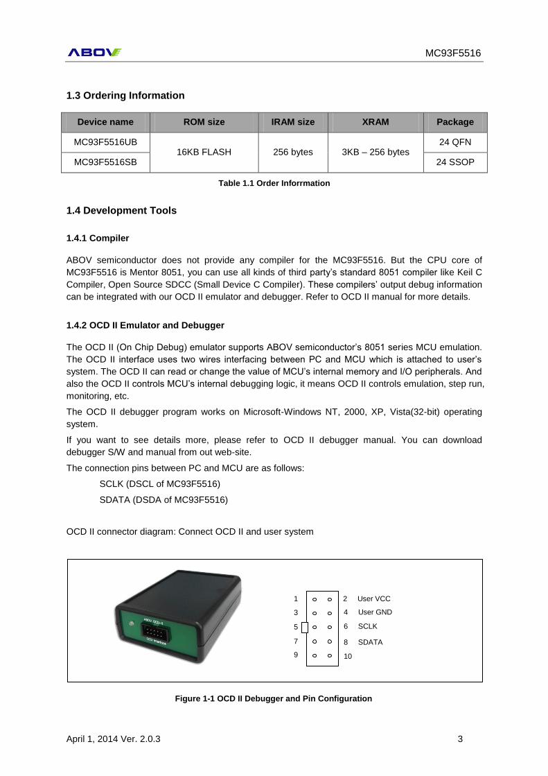
1.4.2 OCD II Emulator and Debugger
The OCD II (On Chip Debug) emulator supports ABOV semiconductor’s 8051 series MCU emulation.
The OCD II interface uses two wires interfacing between PC and MCU which is attached to user’s
system. The OCD II can read or change the value of MCU’s internal memory and I/O peripherals. And
also the OCD II controls MCU’s internal debugging logic, it means OCD II controls emulation, step run,
monitoring, etc.
The OCD II debugger program works on Microsoft-Windows NT, 2000, XP, Vista(32-bit) operating
system.
If you want to see details more, please refer to OCD II debugger manual. You can download
debugger S/W and manual from out web-site.
The connection pins between PC and MCU are as follows:
SCLK (DSCL of MC93F5516)
SDATA (DSDA of MC93F5516)
OCD II connector diagram: Connect OCD II and user system
Figure 1-1 OCD II Debugger and Pin Configuration
2 User VCC
4 User GND
6 SCLK
8 SDATA
10
1
3
5
7
9
MC93F5516
4 April 1, 2014 Ver. 2.0.3
1.4.3 Programmer
To program user code into the ROM of MC93F5516, ABOV semiconductor provides several tools. As
a single programmer, which can program only one chip at a time, there are PGMPlus for parallel
programming and OCD II for serial programming and debugging. On the other hand, you can program
multi-chips at a time by using a gang programmer, which can program up to 8 devices at once.
1.4.3.1 Single Programmer
S-PGM+BLU : BLU dedicated ‘S-PGM+BLU’ is used as a single writer. It is different from ABOV’s
general ‘S-PGM+BLU’ in both software and hardware.
OCD II Emulator: You can program or debug the MCU via OCD II. Because the OCD II supports
ISP(In System Programming), it does not require additional H/W except for developer’s target system.
1.4.3.2 Gang Programmer
The gang programmer can program 8 MCUs at a time. So it is mainly used in mass production line.
The gang programmer is standalone type, thus it does not require host PC.
Figure 1-2 S-PGM + BLU (Single Writer)
Figure 1-3 Gang Programmer
MC93F5516
April 1, 2014 Ver. 2.0.3 5
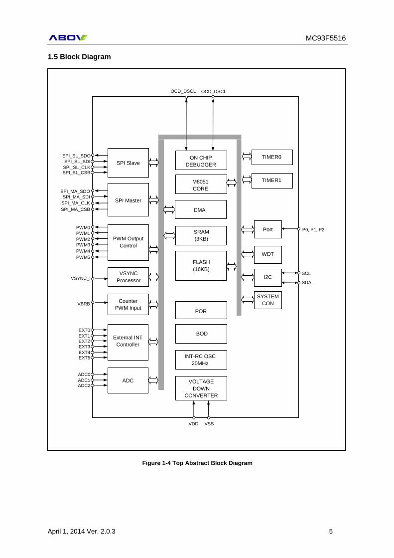
1.5 Block Diagram
Figure 1-4 Top Abstract Block Diagram
ON CHIP
DEBUGGER
OCD_DSCL
M8051
CORE
SRAM
(3KB)
FLASH
(16KB)
POR
BOD
INT-RC OSC
20MHz
VOLTAGE
DOWN
CONVERTER
Port
WDT
TIMER0
Counter
PWM Input
OCD_DSCL
VBRB
P0, P1, P2
VDD VSS
SPI Slave
PWM Output
Control
VSYNC
Processor
SPI_SL_SDO
PWM2
PWM3
PWM4
PWM5
SPI Master
SPI_MA_SDO
SPI_MA_SDI
SPI_MA_CLK
SPI_MA_CSB
I2C
SCL
SDA VSYNC_I
PWM0
PWM1
SPI_SL_SDI
SPI_SL_CLK
SYSTEM
CON
DMA
TIMER1
SPI_SL_CSB
ADC
ADC0
ADC1 ADC2
External INT
Controller
EXT0
EXT1 EXT2
EXT3
EXT4 EXT5
MC93F5516
6 April 1, 2014 Ver. 2.0.3
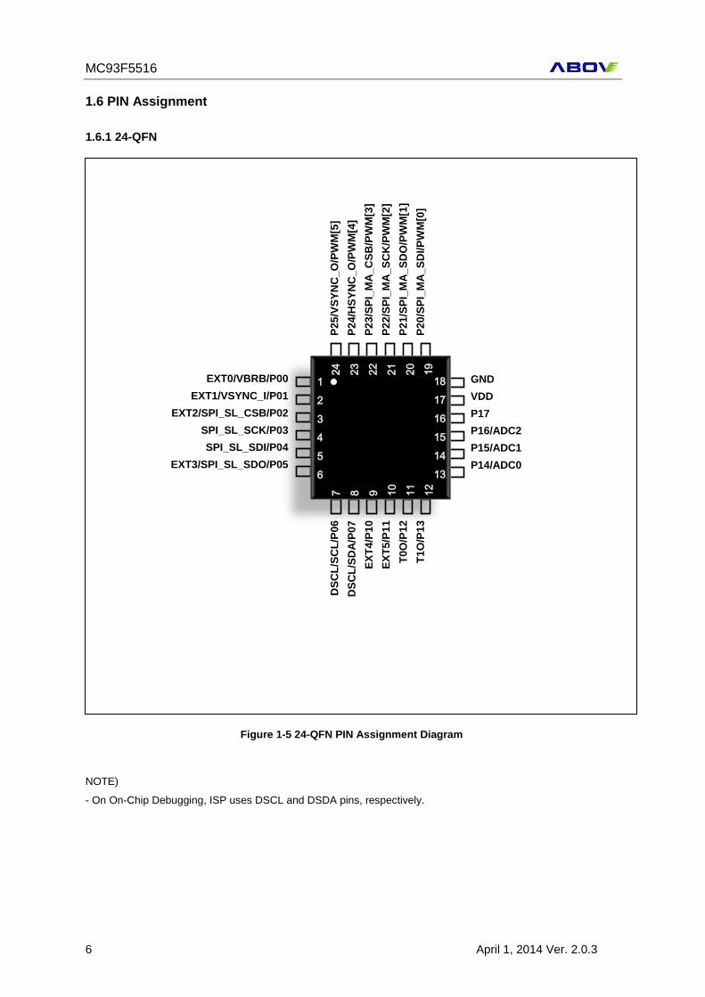
1.6 PIN Assignment
1.6.1 24-QFN
NOTE)
- On On-Chip Debugging, ISP uses DSCL and DSDA pins, respectively.
Figure 1-5 24-QFN PIN Assignment Diagram
EXT0/VBRB/P00
EXT1/VSYNC_I/P01
EXT2/SPI_SL_CSB/P02
SPI_SL_SCK/P03
SPI_SL_SDI/P04
EXT3/SPI_SL_SDO/P05
P2
5/V
SY
NC
_O
/PW
M[5
]
P2
4/H
SY
NC
_O
/PW
M[4
]
P2
3/S
PI_
MA
_C
SB
/PW
M[3
]
P2
2/S
PI_
MA
_S
CK
/PW
M[2
]
P2
1/S
PI_
MA
_S
DO
/PW
M[1
]
P2
0/S
PI_
MA
_S
DI/
PW
M[0
]
GND
VDD
P17
P16/ADC2
P15/ADC1
P14/ADC0
DS
CL
/SC
L/P
06
DS
CL
/SD
A/P
07
EX
T4
/P1
0
EX
T5
/P1
1
T0
O/P
12
T1
O/P
13
1
2
3
4
5
6
18
17
16
15
14
13
7
8
9
10
11
12
24
23
22
21
20
19
MC93F5516
April 1, 2014 Ver. 2.0.3 7
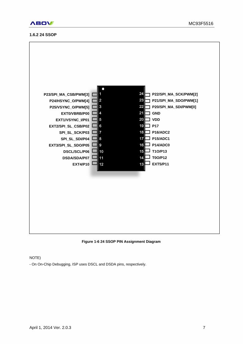
1.6.2 24 SSOP
NOTE)
- On On-Chip Debugging, ISP uses DSCL and DSDA pins, respectively.
Figure 1-6 24 SSOP PIN Assignment Diagram
P23/SPI_MA_CSB/PWM[3]
P24/HSYNC_O/PWM[4]
P25/VSYNC_O/PWM[5]
EXT0/VBRB/P00
EXT1/VSYNC_I/P01
EXT2/SPI_SL_CSB/P02
SPI_SL_SCK/P03
SPI_SL_SDI/P04
EXT3/SPI_SL_SDO/P05
DSCL/SCL/P06
DSDA/SDA/P07
EXT4/P10
P22/SPI_MA_SCK/PWM[2]
P21/SPI_MA_SDO/PWM[1]
P20/SPI_MA_SDI/PWM[0]
GND
VDD
P17
P16/ADC2
P15/ADC1
P14/ADC0
T1O/P13
T0O/P12
EXT5/P11
1
2
3
4
5
6
7
8
9
10
11
12
24
23
22
21
20
19
18
17
16
15
14
13
MC93F5516
8 April 1, 2014 Ver. 2.0.3
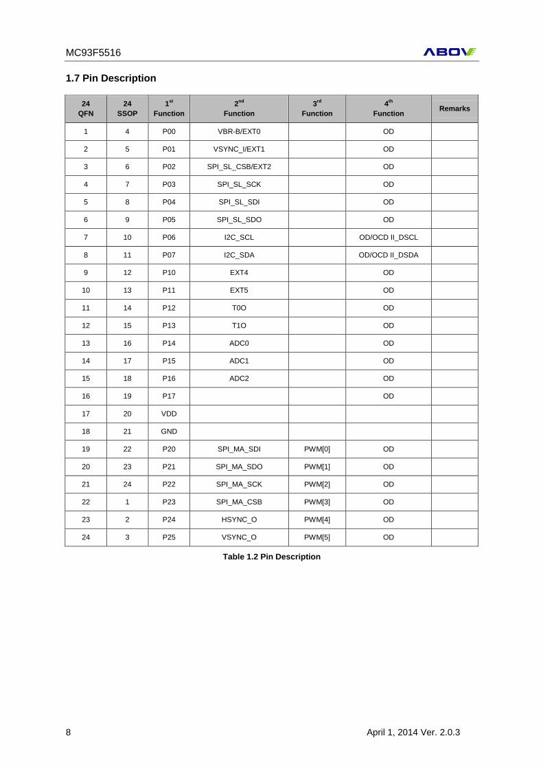
1.7 Pin Description
24
QFN
24
SSOP
1st
Function
2nd
Function
3rd
Function
4th
Function Remarks
1 4 P00 VBR-B/EXT0 OD
2 5 P01 VSYNC_I/EXT1 OD
3 6 P02 SPI_SL_CSB/EXT2 OD
4 7 P03 SPI_SL_SCK OD
5 8 P04 SPI_SL_SDI OD
6 9 P05 SPI_SL_SDO
OD
7 10 P06 I2C_SCL OD/OCD II_DSCL
8 11 P07 I2C_SDA OD/OCD II_DSDA
9 12 P10 EXT4 OD
10 13 P11 EXT5 OD
11 14 P12 T0O OD
12 15 P13 T1O OD
13 16 P14 ADC0 OD
14 17 P15 ADC1 OD
15 18 P16 ADC2 OD
16 19 P17 OD
17 20 VDD
18 21 GND
19 22 P20 SPI_MA_SDI PWM[0] OD
20 23 P21 SPI_MA_SDO PWM[1] OD
21 24 P22 SPI_MA_SCK PWM[2] OD
22 1 P23 SPI_MA_CSB PWM[3] OD
23 2 P24 HSYNC_O PWM[4] OD
24 3 P25 VSYNC_O PWM[5] OD
Table 1.2 Pin Description
MC93F5516
April 1, 2014 Ver. 2.0.3 9
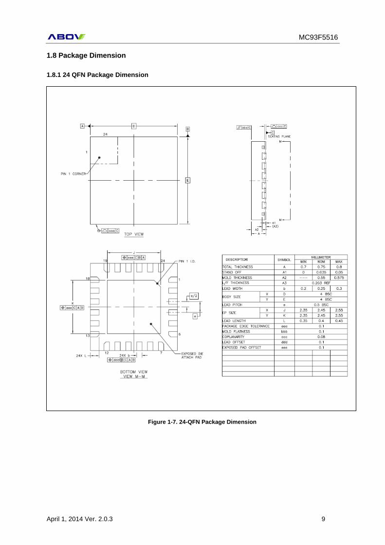
1.8 Package Dimension
1.8.1 24 QFN Package Dimension
Figure 1-7. 24-QFN Package Dimension
MC93F5516
10 April 1, 2014 Ver. 2.0.3
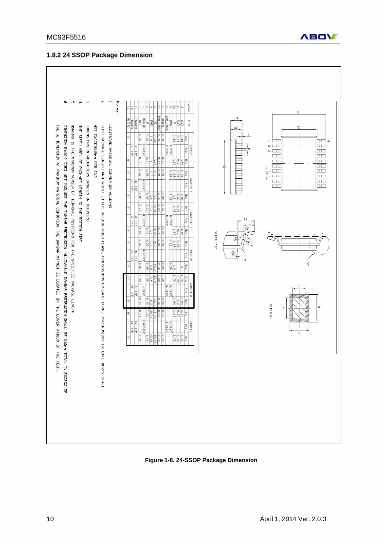
1.8.2 24 SSOP Package Dimension
Figure 1-8. 24-SSOP Package Dimension
MC93F5516
April 1, 2014 Ver. 2.0.3 11
2. Ports
The MC93F5516 have three I/O ports (P0, P1 and P2). Each port can be easily configured by
software as I/O pin, internal pull up and open drain pin to meet various system configurations and
design requirements.
2.1 Port Register
2.1.1 Data Register (PxDA)
Data Register is a bidirectional I/O port. If ports are configured as output ports, data can be written to
the corresponding bit of the PxDA. If ports are configured as input ports, the data can be read from
the corresponding bit of the PxDA.
2.1.2 Direction Register (PxDIR)
Each I/O pin can independently used as an input or an output through the PxIO register. Bits cleared
in this read/write register will select the corresponding pin in Px to become an input, setting a bit sets
the pin to output. All bits are cleared by a system reset.
2.1.3 Pull-up Resistor Selection Register (PxPU)
The on-chip pull-up resistor can be connected to them in 1-bit units with a pull-up resistor selection
register (PxPU). The pull-up register selection controls the pull-up resister enable/disable of each port.
When the corresponding bit is 1, the pull-up resister of the pin is enabled. When 0, the pull-up resister
is disabled. All bits are cleared by a system reset.
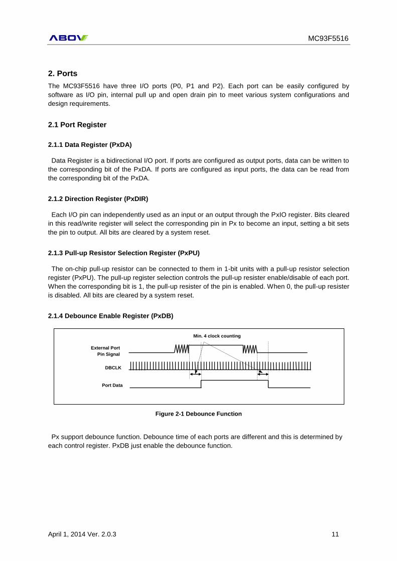
2.1.4 Debounce Enable Register (PxDB)
Figure 2-1 Debounce Function
Px support debounce function. Debounce time of each ports are different and this is determined by
each control register. PxDB just enable the debounce function.
External Port
Pin Signal
DBCLK
Port Data
Min. 4 clock counting
MC93F5516
12 April 1, 2014 Ver. 2.0.3
24
QFN
24
SOP PIN Description MAPPING
1 4 VBRB/EXT0/P00 Debounce Logic (4*(PWM_DB+1) System Clock) P0[0]
2 5 VSYNC_I/EXT1 Debounce Logic (4*(VSYNC_DB+1) System Clock) P0[1]
3 6 SPI_CSB/EXT2/GPIO0 Debounce Logic((2*SPI_SL_DB)+1,
if SPI_MA_DB=0, then 2) P0[2]
4 7 SPI_SCK Dual VIH/VIL, Debounce Logic((2*SPI_SL_DB)+1,
if SPI_MA_DB=0, then 2) P0[3]
5 8 SPI_SDI Dual VIH/VIL, Debounce Logic((2*SPI_SL_DB)+1,
if SPI_MA_DB=0, then 2) P0[4]
6 9 SPI_SDO/EXT3/GPIO1 Debounce Logic (5 System Clock) P0[5]
7 10 I2C_SCL/OCD_DSCL Debounce Logic (5 System Clock) P0[6]
8 11 I2C_SDA/OCD_DSDA Debounce Logic (5 System Clock) P0[7]
9 12 EXT4/GPIO2 Debounce Logic (5 System Clock) P1[0]
10 13 EXT5/GPIO3 Debounce Logic (5 System Clock) P1[1]
11 14 T0O/GPIO4 Not supported P1[2]
12 15 T1O/GPIO5 Not supported P1[3]
13 16 ADC0 Not supported P1[4]
14 17 ADC1 Not supported P1[5]
15 18 ADC2/GPIO6 Not supported P1[6]
16 19 GPIO7 Not supported P1[7]
17 20 VDD Not supported
18 21 GND Not supported
19 22 PWM[0]/SPI_SDI Debounce Logic((2*SPI_MA_DB)+1,
if SPI_MA_DB=0, then 2) P2[0]
20 23 PWM[1]/SPI_SDO Not supported P2[1]
21 24 PWM[2]/SPI_SCK Not supported P2[2]
22 1 PWM[3]/SPI_CSB Not supported P2[3]
23 2 PWM[4]/HSYNC_O Not supported P2[4]
24 3 PWM[5]/VSYNC_O Not supported P2[5]
Table 2.1 Debounce Table
MC93F5516
April 1, 2014 Ver. 2.0.3 13
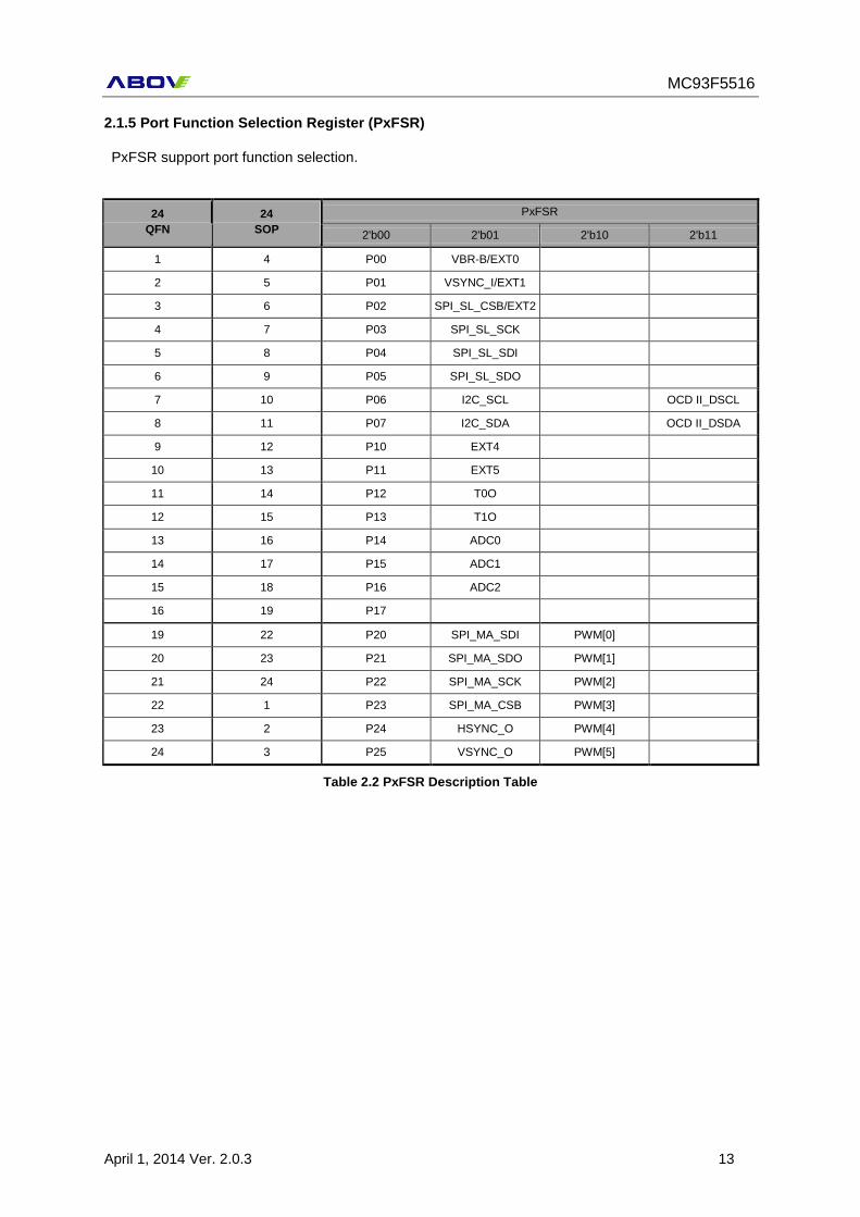
2.1.5 Port Function Selection Register (PxFSR)
PxFSR support port function selection.
24
QFN
24
SOP
PxFSR
2'b00 2'b01 2'b10 2'b11
1 4 P00 VBR-B/EXT0
2 5 P01 VSYNC_I/EXT1
3 6 P02 SPI_SL_CSB/EXT2
4 7 P03 SPI_SL_SCK
5 8 P04 SPI_SL_SDI
6 9 P05 SPI_SL_SDO
7 10 P06 I2C_SCL
OCD II_DSCL
8 11 P07 I2C_SDA
OCD II_DSDA
9 12 P10 EXT4
10 13 P11 EXT5
11 14 P12 T0O
12 15 P13 T1O
13 16 P14 ADC0
14 17 P15 ADC1
15 18 P16 ADC2
16 19 P17
19 22 P20 SPI_MA_SDI PWM[0]
20 23 P21 SPI_MA_SDO PWM[1]
21 24 P22 SPI_MA_SCK PWM[2]
22 1 P23 SPI_MA_CSB PWM[3]
23 2 P24 HSYNC_O PWM[4]
24 3 P25 VSYNC_O PWM[5]
Table 2.2 PxFSR Description Table
MC93F5516
14 April 1, 2014 Ver. 2.0.3
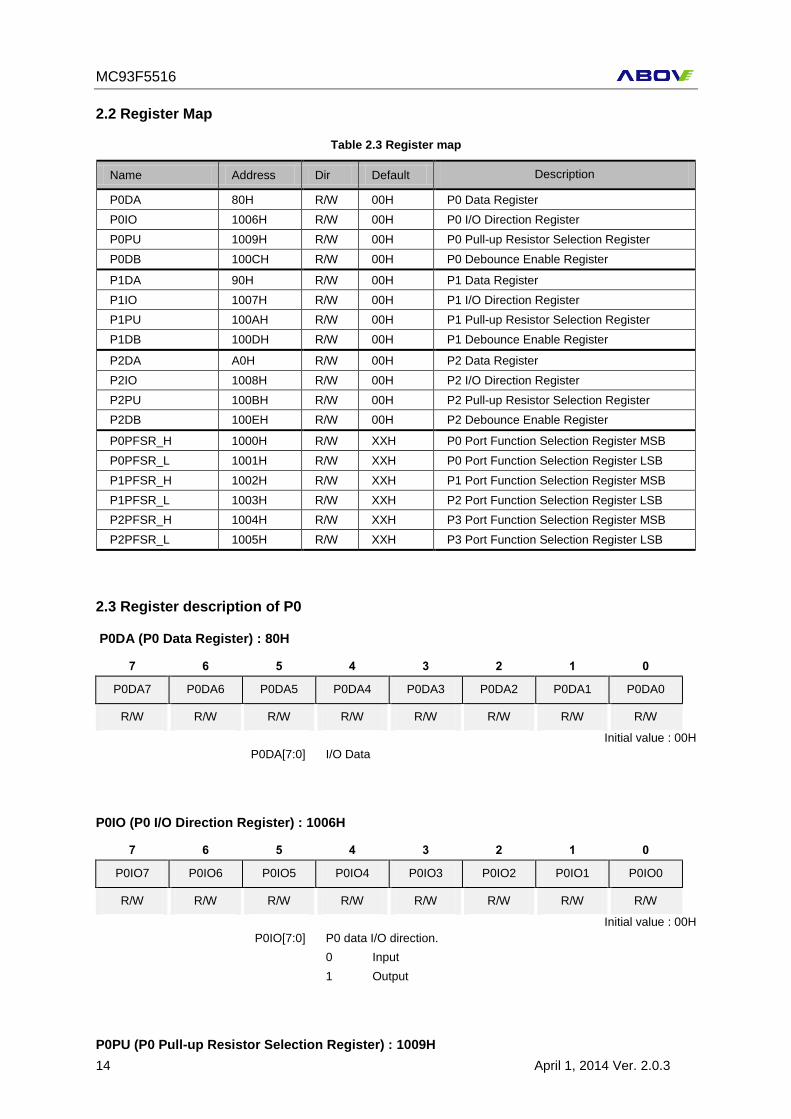
2.2 Register Map
Table 2.3 Register map
Name Address Dir Default Description
P0DA 80H R/W 00H P0 Data Register
P0IO 1006H R/W 00H P0 I/O Direction Register
P0PU 1009H R/W 00H P0 Pull-up Resistor Selection Register
P0DB 100CH R/W 00H P0 Debounce Enable Register
P1DA 90H R/W 00H P1 Data Register
P1IO 1007H R/W 00H P1 I/O Direction Register
P1PU 100AH R/W 00H P1 Pull-up Resistor Selection Register
P1DB 100DH R/W 00H P1 Debounce Enable Register
P2DA A0H R/W 00H P2 Data Register
P2IO 1008H R/W 00H P2 I/O Direction Register
P2PU 100BH R/W 00H P2 Pull-up Resistor Selection Register
P2DB 100EH R/W 00H P2 Debounce Enable Register
P0PFSR_H 1000H R/W XXH P0 Port Function Selection Register MSB
P0PFSR_L 1001H R/W XXH P0 Port Function Selection Register LSB
P1PFSR_H 1002H R/W XXH P1 Port Function Selection Register MSB
P1PFSR_L 1003H R/W XXH P2 Port Function Selection Register LSB
P2PFSR_H 1004H R/W XXH P3 Port Function Selection Register MSB
P2PFSR_L 1005H R/W XXH P3 Port Function Selection Register LSB
2.3 Register description of P0
P0DA (P0 Data Register) : 80H
7 6 5 4 3 2 1 0
P0DA7 P0DA6 P0DA5 P0DA4 P0DA3 P0DA2 P0DA1 P0DA0
R/W R/W R/W R/W R/W R/W R/W R/W
Initial value : 00H
P0DA[7:0] I/O Data
P0IO (P0 I/O Direction Register) : 1006H
7 6 5 4 3 2 1 0
P0IO7 P0IO6 P0IO5 P0IO4 P0IO3 P0IO2 P0IO1 P0IO0
R/W R/W R/W R/W R/W R/W R/W R/W
Initial value : 00H
P0IO[7:0] P0 data I/O direction.
0 Input
1 Output
P0PU (P0 Pull-up Resistor Selection Register) : 1009H
MC93F5516
April 1, 2014 Ver. 2.0.3 15
7 6 5 4 3 2 1 0
P0PU7 P0PU6 P0PU5 P0PU4 P0PU3 P0PU2 P0PU1 P0PU0
R/W R/W R/W R/W R/W R/W R/W R/W
Initial value : 00H
P0PU[7:0] Configure pull-up resistor of P0 port
0 disable
1 enable
P0DB (P0 Debounce Enable Register) : 100CH
7 6 5 4 3 2 1 0
P0DB7 P0DB6 P0DB5 P0DB4 P0DB3 P0DB2 P0DB1 P0DB0
R/W R/W R/W R/W R/W R/W R/W R/W
Initial value : 00H
P0DB[7:0] Configure debounce of P0 port
0 disable
1 enable
Note : When it is used as a VSYNC or SPI_SL_CSB, P0DB1 or P0DB2 can be set individually. But
P0DB1 and P0DB2 must be set together when one of those port is used as a general purpose input
port and it requires the debounce enable.
P0FSR_H (P0 Function Selection Register MSB) : 1000H
7 6 5 4 3 2 1 0
P0FSR15 P0FSR14 P0FSR13 P0FSR12 P0FSR11 P0FSR10 P0FSR09 P0FSR08
R/W R/W R/W R/W R/W R/W R/W R/W
Initial value : xxH
P0FSR [15:14] P07 Function Selection
0 0 P07
0 1 I2C_SDA
1 0 Reserved
1 1 OCD_DSDA
P0FSR [13:12] P06 Function Selection
0 0 P06
0 1 I2C_SCL
1 0 Reserved
1 1 OCD_DSCL
P0FSR [11:10] P05 Function Selection
0 0 P05
0 1 SPI_SL_SDO
1 0 EXT3
1 1 Reserved
P0FSR [9:8] P04 Function Selection
0 0 P04
0 1 SPI_SL_SDI
1 0 Reserved
1 1 Reserved
P0FSR_L (P0 Function Selection Register LSB) : 1001H
MC93F5516
16 April 1, 2014 Ver. 2.0.3
7 6 5 4 3 2 1 0
P0FSR07 P0FS06 P0FSR05 P0FSR04 P0FSR03 P0FSR02 P0FSR01 P0FSR00
R/W R/W R/W R/W R/W R/W R/W R/W
Initial value : xxH
P0FSR [7:6] P03 Function Selection
0 0 P03
0 1 SPI_SL_SCK
1 0 Reserved
1 1 Reserved
P0FSR [5:4] P02 Function Selection
0 0 P02
0 1 SPI_SL_CSB/EXT2
1 0 Reserved
1 1 Reserved
P0FSR [3:2] P01 Function Selection
0 0 P01
0 1 VSYNC_I/EXT1
1 0 Reserved
1 1 Reserved
P0FSR [1:0] P00 Function Selection
0 0 P00
0 1 VBRB/EXT0
1 0 Reserved
1 1 Reserved
2.4 Register description for P1
P1DA (P1 Data Register) : 90H
7 6 5 4 3 2 1 0
P1DA7 P1DA6 P1DA5 P1DA4 P1DA3 P1DA2 P1DA1 P1DA0
R/W R/W R/W R/W R/W R/W R/W R/W
Initial value : 00H
P1DA[7:0] I/O Data
P1IO (P1 I/O Direction Register) : 1007H
7 6 5 4 3 2 1 0
P0IO7 P0IO6 P0IO5 P0IO4 P0IO3 P0IO2 P0IO1 P0IO0
R/W R/W R/W R/W R/W R/W R/W R/W
Initial value : 00H
P1IO[7:0] P1 data I/O direction.
0 Input
1 Output
P1PU (P1 Pull-up Resistor Selection Register) : 100AH
MC93F5516
April 1, 2014 Ver. 2.0.3 17
7 6 5 4 3 2 1 0
P1PU7 P1PU6 P1PU5 P1PU4 P1PU3 P1PU2 P1PU1 P1PU0
R/W R/W R/W R/W R/W R/W R/W R/W
Initial value : 00H
P1PU[7:0] Configure pull-up resistor of P1 port
0 Disable
1 Enable
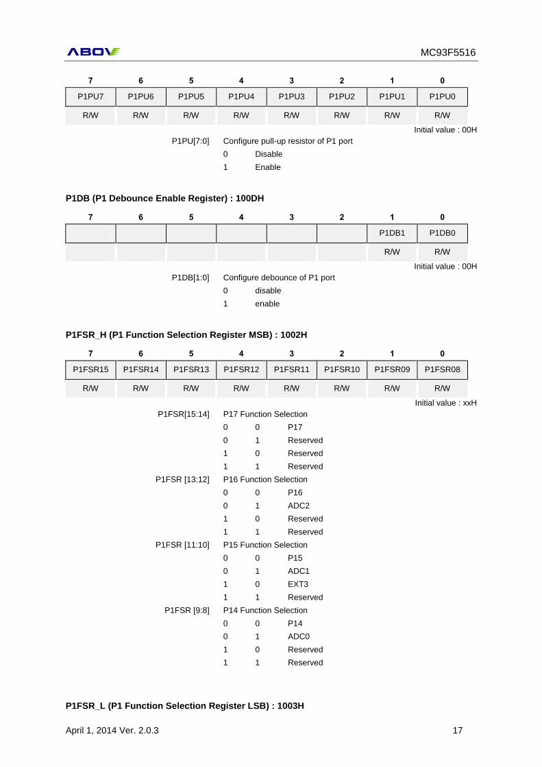
P1DB (P1 Debounce Enable Register) : 100DH
7 6 5 4 3 2 1 0
P1DB1 P1DB0
R/W R/W
Initial value : 00H
P1DB[1:0] Configure debounce of P1 port
0 disable
1 enable
P1FSR_H (P1 Function Selection Register MSB) : 1002H
7 6 5 4 3 2 1 0
P1FSR15 P1FSR14 P1FSR13 P1FSR12 P1FSR11 P1FSR10 P1FSR09 P1FSR08
R/W R/W R/W R/W R/W R/W R/W R/W
Initial value : xxH
P1FSR[15:14] P17 Function Selection
0 0 P17
0 1 Reserved
1 0 Reserved
1 1 Reserved
P1FSR [13:12] P16 Function Selection
0 0 P16
0 1 ADC2
1 0 Reserved
1 1 Reserved
P1FSR [11:10] P15 Function Selection
0 0 P15
0 1 ADC1
1 0 EXT3
1 1 Reserved
P1FSR [9:8] P14 Function Selection
0 0 P14
0 1 ADC0
1 0 Reserved
1 1 Reserved
P1FSR_L (P1 Function Selection Register LSB) : 1003H
MC93F5516
18 April 1, 2014 Ver. 2.0.3
7 6 5 4 3 2 1 0
P1FSR07 P1FS06 P1FSR05 P1FSR04 P1FSR03 P1FSR02 P1FSR01 P1FSR00
R/W R/W R/W R/W R/W R/W R/W R/W
Initial value : xxH
P1FSR [7:6] P13 Function Selection
0 0 P13
0 1 T1O
1 0 Reserved
1 1 Reserved
P1FSR [5:4] P12 Function Selection
0 0 P12
0 1 T0O
1 0 Reserved
1 1 Reserved
P1FSR [3:2] P11 Function Selection
0 0 P11
0 1 EXT5
1 0 Reserved
1 1 Reserved
P1FSR [1:0] P10 Function Selection
0 0 P10
0 1 EXT4
1 0 Reserved
1 1 Reserved
2.5 Register description for P2
P2DA (P2 Data Register) : A0H
7 6 5 4 3 2 1 0
- - P2DA5 P2DA4 P2DA3 P2DA2 P2DA1 P2DA0
- - R/W R/W R/W R/W R/W R/W
Initial value : 00H
P2DA[5:0] I/O Data
P2IO (P2 I/O Direction Register) : 1008H
7 6 5 4 3 2 1 0
- - P2IO5 P2IO4 P2IO3 P2IO2 P2IO1 P2IO0
- - R/W R/W R/W R/W R/W R/W
Initial value : 00H
P2IO[5:0] P2 data I/O direction.
0 Input
1 Output
P2PU (P2 Pull-up Resistor Selection Register) : 100BH
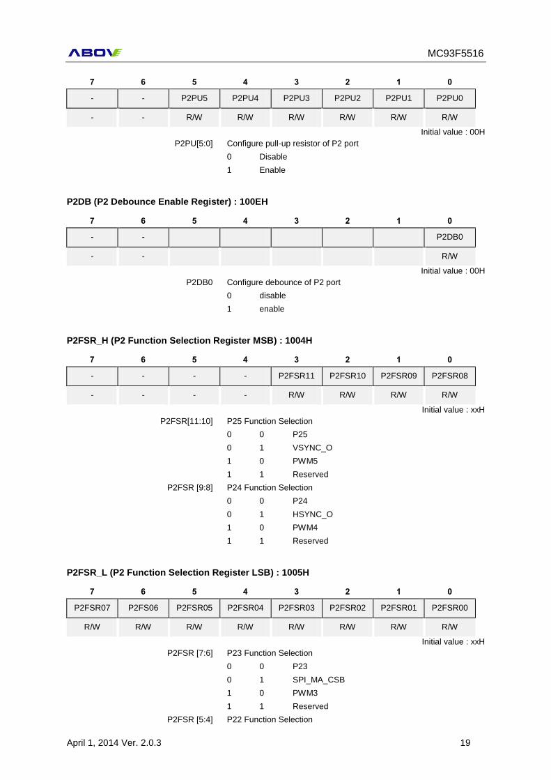
MC93F5516
April 1, 2014 Ver. 2.0.3 19
7 6 5 4 3 2 1 0
- - P2PU5 P2PU4 P2PU3 P2PU2 P2PU1 P2PU0
- - R/W R/W R/W R/W R/W R/W
Initial value : 00H
P2PU[5:0] Configure pull-up resistor of P2 port
0 Disable
1 Enable
P2DB (P2 Debounce Enable Register) : 100EH
7 6 5 4 3 2 1 0
- - P2DB0
- - R/W
Initial value : 00H
P2DB0 Configure debounce of P2 port
0 disable
1 enable
P2FSR_H (P2 Function Selection Register MSB) : 1004H
7 6 5 4 3 2 1 0
- - - - P2FSR11 P2FSR10 P2FSR09 P2FSR08
- - - - R/W R/W R/W R/W
Initial value : xxH
P2FSR[11:10] P25 Function Selection
0 0 P25
0 1 VSYNC_O
1 0 PWM5
1 1 Reserved
P2FSR [9:8] P24 Function Selection
0 0 P24
0 1 HSYNC_O
1 0 PWM4
1 1 Reserved
P2FSR_L (P2 Function Selection Register LSB) : 1005H
7 6 5 4 3 2 1 0
P2FSR07 P2FS06 P2FSR05 P2FSR04 P2FSR03 P2FSR02 P2FSR01 P2FSR00
R/W R/W R/W R/W R/W R/W R/W R/W
Initial value : xxH
P2FSR [7:6] P23 Function Selection
0 0 P23
0 1 SPI_MA_CSB
1 0 PWM3
1 1 Reserved
P2FSR [5:4] P22 Function Selection
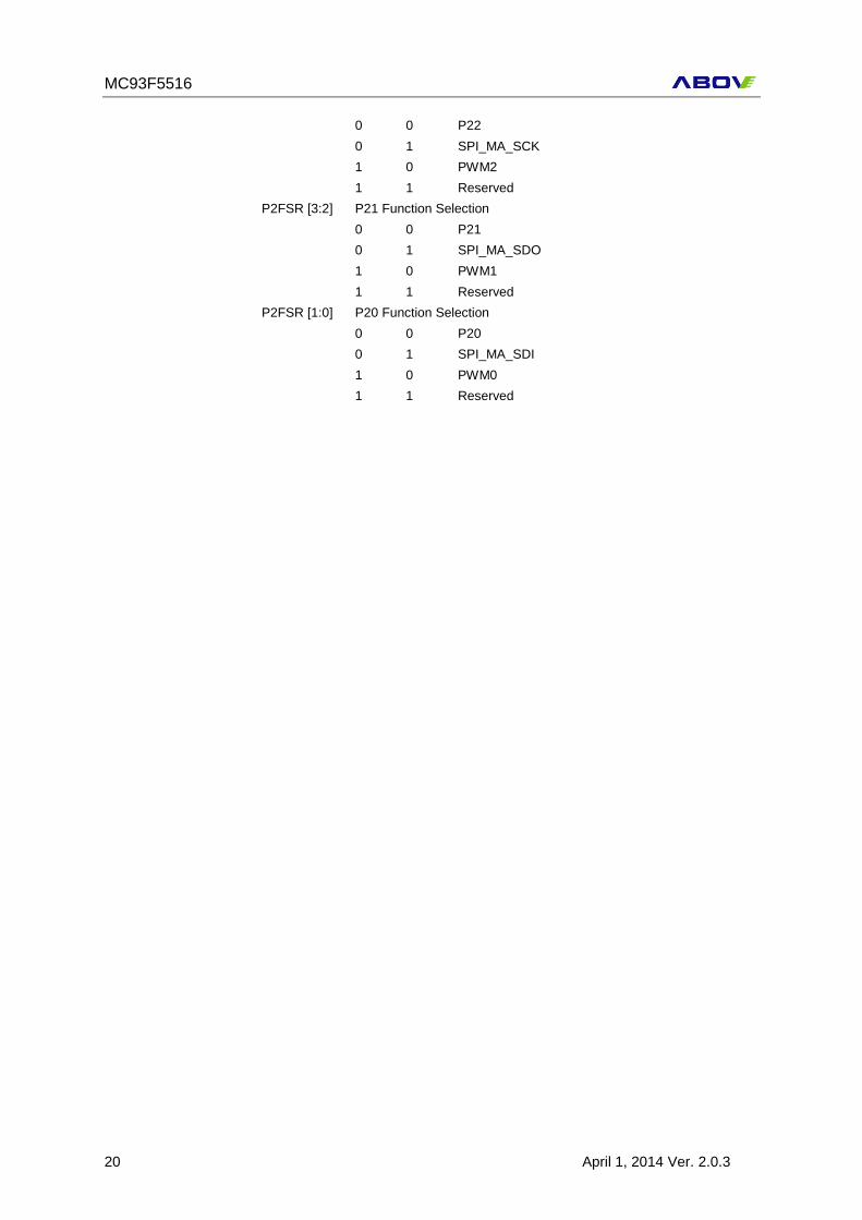
MC93F5516
20 April 1, 2014 Ver. 2.0.3
0 0 P22
0 1 SPI_MA_SCK
1 0 PWM2
1 1 Reserved
P2FSR [3:2] P21 Function Selection
0 0 P21
0 1 SPI_MA_SDO
1 0 PWM1
1 1 Reserved
P2FSR [1:0] P20 Function Selection
0 0 P20
0 1 SPI_MA_SDI
1 0 PWM0
1 1 Reserved
MC93F5516
April 1, 2014 Ver. 2.0.3 21
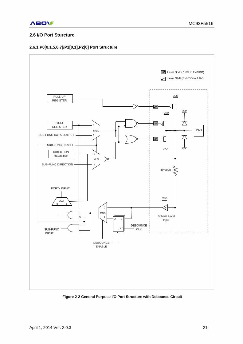
2.6 I/O Port Sturcture
2.6.1 P0[0,1,5,6,7]/P1[0,1],P2[0] Port Structure
VDD
VDD VDD
PAD
SUB-FUNC ENABLE
Level Shift ( 1.8V to ExtVDD)
Level Shift (ExtVDD to 1.8V)
DATA
REGISTER
PULL-UP
REGISTER
SUB-FUNC DATA OUTPUT
DIRECTION
REGISTER
SUB-FUNC DIRECTION
0
1
MUX
MUX
0
1
0
1
MUX
r
D
CP
Q
DEBOUNCE
CLK
DEBOUNCE
ENABLE
PORTx INPUT
SUB-FUNC
INPUT
R(400Ω)
Schmitt Level
Input
MUX
1 0
VDD
Figure 2-2 General Purpose I/O Port Structure with Debounce Circuit
MC93F5516
22 April 1, 2014 Ver. 2.0.3
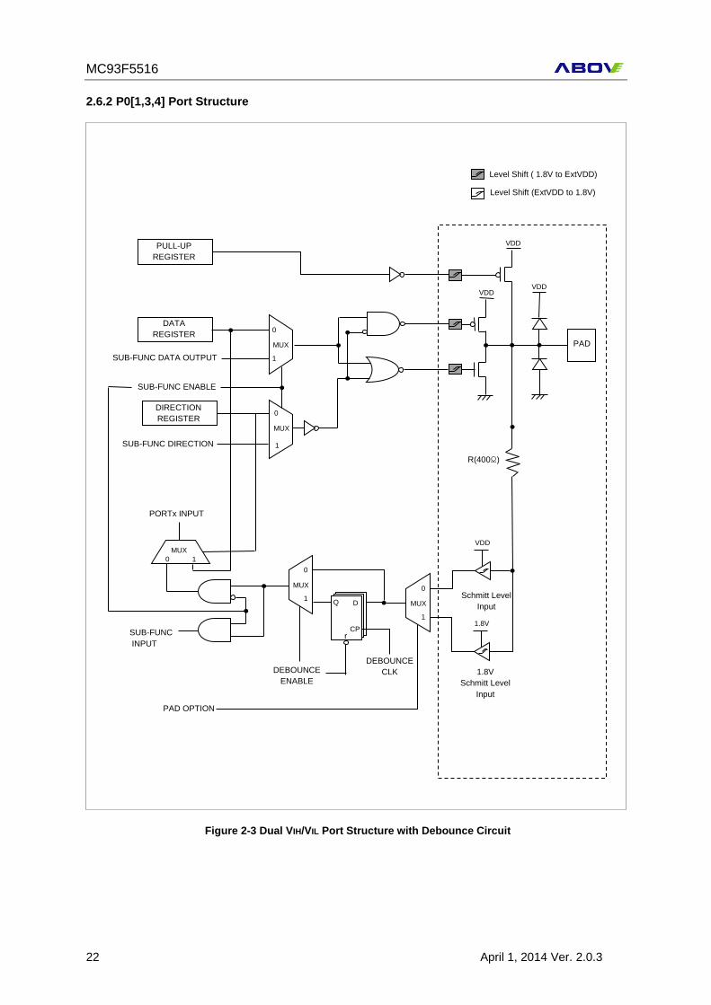
2.6.2 P0[1,3,4] Port Structure
VDD
VDD VDD
PAD
SUB-FUNC ENABLE
Level Shift ( 1.8V to ExtVDD)
Level Shift (ExtVDD to 1.8V)
DATA
REGISTER
PULL-UP
REGISTER
SUB-FUNC DATA OUTPUT
DIRECTION
REGISTER
SUB-FUNC DIRECTION
0
1
MUX
MUX
0
1
0
1
MUX
r
D
CP
Q
DEBOUNCE
CLK DEBOUNCE
ENABLE
PORTx INPUT
SUB-FUNC
INPUT
R(400Ω)
Schmitt Level
Input
MUX
1 0
1.8V
Schmitt Level
Input
0
1
MUX
PAD OPTION
VDD
1.8V
Figure 2-3 Dual VIH/VIL Port Structure with Debounce Circuit
MC93F5516
April 1, 2014 Ver. 2.0.3 23
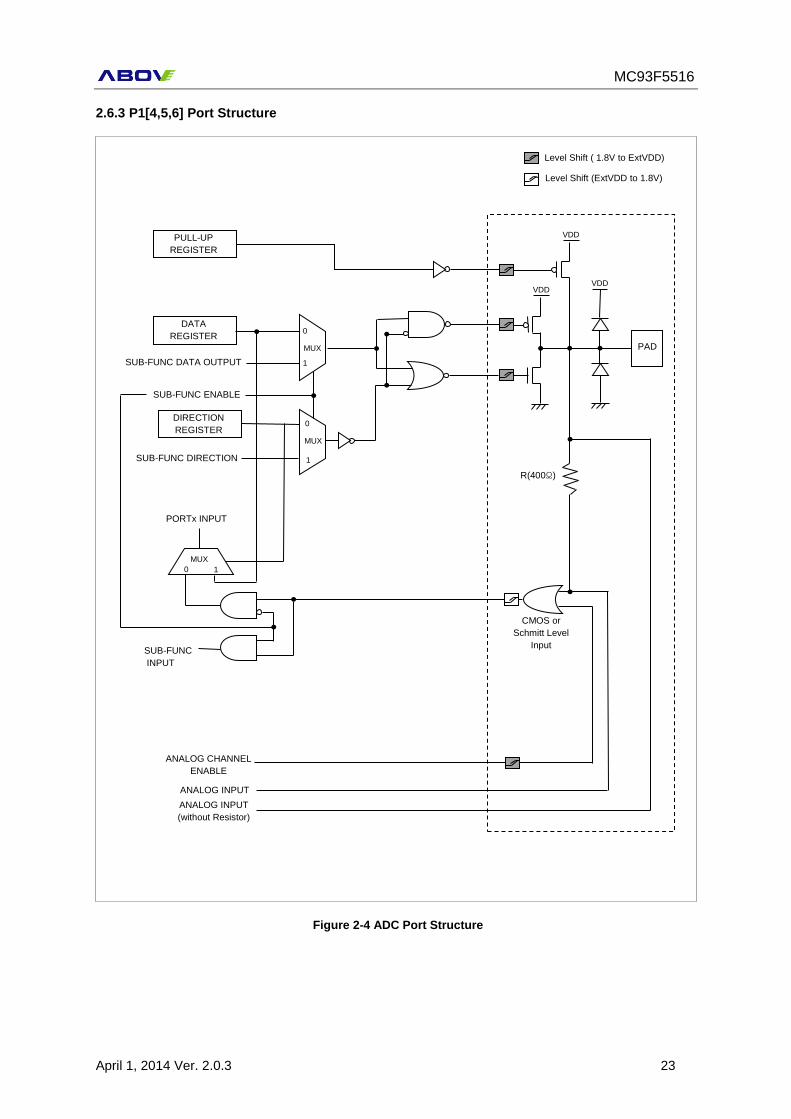
2.6.3 P1[4,5,6] Port Structure
VDD
VDD VDD
PAD
SUB-FUNC ENABLE
Level Shift ( 1.8V to ExtVDD)
Level Shift (ExtVDD to 1.8V)
DATA
REGISTER
PULL-UP
REGISTER
SUB-FUNC DATA OUTPUT
DIRECTION
REGISTER
SUB-FUNC DIRECTION
0
1
MUX
MUX
0
1
PORTx INPUT
SUB-FUNC
INPUT
ANALOG CHANNEL
ENABLE
ANALOG INPUT
ANALOG INPUT
(without Resistor)
R(400Ω)
CMOS or
Schmitt Level
Input
MUX
1 0
Figure 2-4 ADC Port Structure
MC93F5516
24 April 1, 2014 Ver. 2.0.3
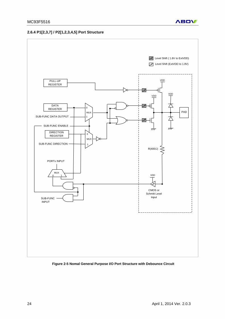
2.6.4 P1[2,3,7] / P2[1,2,3,4,5] Port Structure
VDD
VDD VDD
PAD
SUB-FUNC ENABLE
Level Shift ( 1.8V to ExtVDD)
Level Shift (ExtVDD to 1.8V)
DATA
REGISTER
PULL-UP
REGISTER
SUB-FUNC DATA OUTPUT
DIRECTION
REGISTER
SUB-FUNC DIRECTION
0
1
MUX
MUX
0
1
PORTx INPUT
SUB-FUNC
INPUT
R(400Ω)
CMOS or
Schmitt Level
Input
MUX
1 0 VDD
Figure 2-5 Nomal General Purpose I/O Port Structure with Debounce Circuit
MC93F5516
April 1, 2014 Ver. 2.0.3 25
3. Memory
MC93F5516 addresses three separate address memory stores: program memory, internal data
memory (used for storing register bank, stack and scratch pad data) and external data memory. All
three memories are logically independent of each other and are accessed through their own interface
signals. External Data Memory can only be accessed by software using dedicated MOVX instructions.
The logical separation of memory allows internal data memory to be assessed by 8-bit address, which
can be more quickly stored and manipulated by 8-bit CPU. 16-bit address for external data memory
can also be generated.
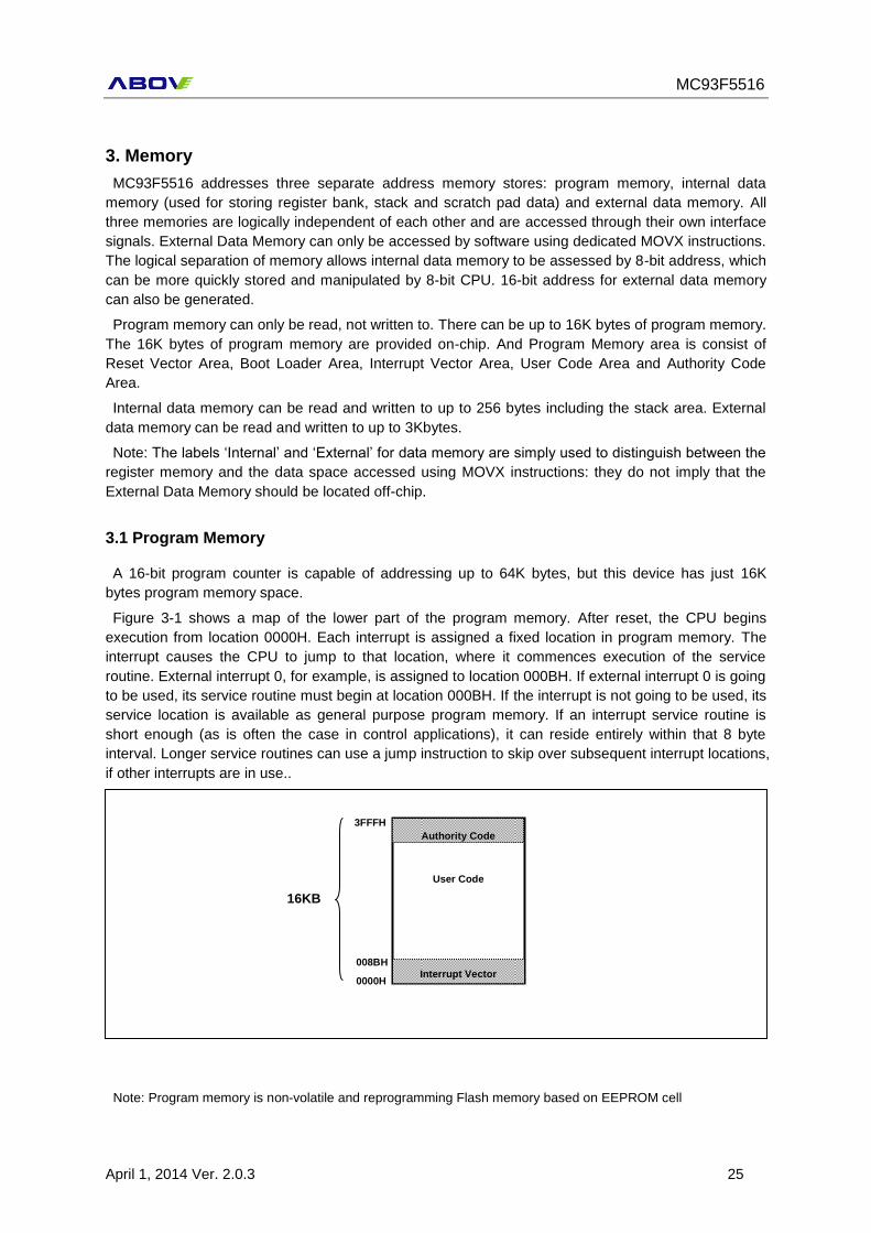
Program memory can only be read, not written to. There can be up to 16K bytes of program memory.
The 16K bytes of program memory are provided on-chip. And Program Memory area is consist of
Reset Vector Area, Boot Loader Area, Interrupt Vector Area, User Code Area and Authority Code
Area.
Internal data memory can be read and written to up to 256 bytes including the stack area. External
data memory can be read and written to up to 3Kbytes.
Note: The labels ‘Internal’ and ‘External’ for data memory are simply used to distinguish between the
register memory and the data space accessed using MOVX instructions: they do not imply that the
External Data Memory should be located off-chip.
3.1 Program Memory
A 16-bit program counter is capable of addressing up to 64K bytes, but this device has just 16K
bytes program memory space.
Figure 3-1 shows a map of the lower part of the program memory. After reset, the CPU begins
execution from location 0000H. Each interrupt is assigned a fixed location in program memory. The
interrupt causes the CPU to jump to that location, where it commences execution of the service
routine. External interrupt 0, for example, is assigned to location 000BH. If external interrupt 0 is going
to be used, its service routine must begin at location 000BH. If the interrupt is not going to be used, its
service location is available as general purpose program memory. If an interrupt service routine is
short enough (as is often the case in control applications), it can reside entirely within that 8 byte
interval. Longer service routines can use a jump instruction to skip over subsequent interrupt locations,
if other interrupts are in use..
Note: Program memory is non-volatile and reprogramming Flash memory based on EEPROM cell
Figure 3-1 Program memory
3FFFH
0000H
16KB
Interrupt Vector 008BH
User Code
Authority Code
MC93F5516
26 April 1, 2014 Ver. 2.0.3
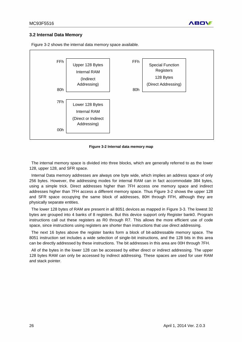
3.2 Internal Data Memory
Figure 3-2 shows the internal data memory space available.
The internal memory space is divided into three blocks, which are generally referred to as the lower
128, upper 128, and SFR space.
Internal Data memory addresses are always one byte wide, which implies an address space of only
256 bytes. However, the addressing modes for internal RAM can in fact accommodate 384 bytes,
using a simple trick. Direct addresses higher than 7FH access one memory space and indirect
addresses higher than 7FH access a different memory space. Thus Figure 3-2 shows the upper 128
and SFR space occupying the same block of addresses, 80H through FFH, although they are
physically separate entities.
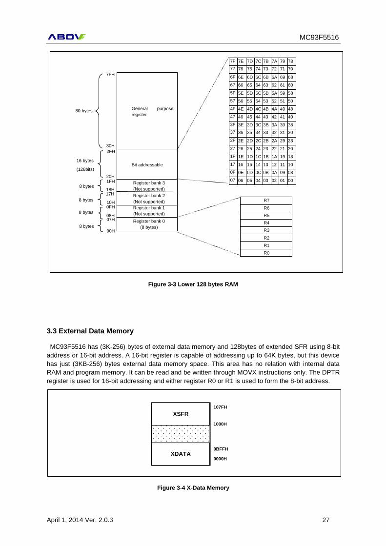
The lower 128 bytes of RAM are present in all 8051 devices as mapped in Figure 3-3. The lowest 32
bytes are grouped into 4 banks of 8 registers. But this device support only Register bank0. Program
instructions call out these registers as R0 through R7. This allows the more efficient use of code
space, since instructions using registers are shorter than instructions that use direct addressing.
The next 16 bytes above the register banks form a block of bit-addressable memory space. The
8051 instruction set includes a wide selection of single-bit instructions, and the 128 bits in this area
can be directly addressed by these instructions. The bit addresses in this area are 00H through 7FH.
All of the bytes in the lower 128 can be accessed by either direct or indirect addressing. The upper
128 bytes RAM can only be accessed by indirect addressing. These spaces are used for user RAM
and stack pointer.
Figure 3-2 Internal data memory map
Upper 128 Bytes
Internal RAM
(Indirect
Addressing)
Special Function
Registers
128 Bytes
(Direct Addressing)
Lower 128 Bytes
Internal RAM
(Direct or Indirect
Addressing)
FFh
80h
7Fh
00h
FFh
80h
MC93F5516
April 1, 2014 Ver. 2.0.3 27
3.3 External Data Memory
MC93F5516 has (3K-256) bytes of external data memory and 128bytes of extended SFR using 8-bit
address or 16-bit address. A 16-bit register is capable of addressing up to 64K bytes, but this device
has just (3KB-256) bytes external data memory space. This area has no relation with internal data
RAM and program memory. It can be read and be written through MOVX instructions only. The DPTR
register is used for 16-bit addressing and either register R0 or R1 is used to form the 8-bit address.
Figure 3-3 Lower 128 bytes RAM
Figure 3-4 X-Data Memory
00 01 02 03 04 05 06 07
08 09 0A 0B 0C 0D 0E 0F
10 11 12 13 14 15 16 17
18 19 1A 1B 1C 1D 1E 1F
20 21 22 23 24 25 26 27
28 29 2A 2B 2C 2D 2E 2F
30 31 32 33 34 35 36 37
38 39 3A 3B 3C 3D 3E 3F
40 41 42 43 44 45 46 47
48 49 4A 4B 4C 4D 4E 4F
50 51 52 53 54 55 56 57
58 59 5A 5B 5C 5D 5E 5F
60 61 62 63 64 65 66 67
68 69 6A 6B 6C 6D 6E 6F
70 71 72 73 74 75 76 77
78 79 7A 7B 7C 7D 7E 7F
R5
R4
R3
R2
R1
R0
R6
R7
2FH
Register bank 0
(8 bytes)
Register bank 1
(Not supported)
Register bank 2
(Not supported)
Register bank 3
(Not supported)
Bit addressable
General purpose
register
20H
18H 17H
10H 0FH
08H 07H
00H
30H
7FH
1FH
80 bytes
16 bytes
(128bits)
8 bytes
8 bytes
8 bytes
8 bytes
0000H XDATA
107FH
1000H
0BFFH
XSFR
MC93F5516
28 April 1, 2014 Ver. 2.0.3
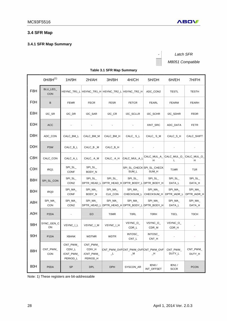
3.4 SFR Map
3.4.1 SFR Map Summary
- Latch SFR
M8051 Compatible
Table 3.1 SFR Map Summary
0H/8H
(1) 1H/9H 2H/AH 3H/BH 4H/CH 5H/DH 6H/EH 7H/FH
F8H BLU_LED_
CON HSYNC_TR1_L HSYNC_TR1_H HSYNC_TR2_L HSYNC_TR2_H ADC_CON2 TESTL TESTH
F0H B FEMR FECR FESR FETCR FEARL FEARM FEARH
E8H I2C_SR I2C_DR I2C_SAR I2C_CR I2C_SCLLR I2C_SCHR I2C_SDHR FEDR
E0H ACC - - - - XINT_SRC ADC_DATA FETR
D8H ADC_CON CALC_BM_L CALC_BM_M CALC_BM_H CALC_ S_L CALC_ S_M CALC_S_H CALC_SHIFT
D0H PSW CALC_B_L CALC_B _M CALC_B_H - - - -
C8H CALC_CON CALC_A_L CALC_ A_M CALC_ A_H CALC_MUL_A_L CALC_MUL_A_
H
CALC_MUL_O_
L
CALC_MUL_O_
H
C0H IRQ1 SPI_SL_
CONF
SPI_SL_
BODY_N
SPI_SL_CHECK
SUM_L
SPI_SL_CHECK
SUM_H T1MR T1R
B8H SPI_SL_CON SPI_SL_
CON2
SPI_SL_
DPTR_HEAD_L
SPI_SL_
DPTR_HEAD_H
SPI_SL_
DPTR_BODY_L
SPI_SL_
DPTR_BODY_H
SPI_SL_
DATA_L
SPI_SL_
DATA_H
B0H IRQ0 SPI_MA_
CONF
SPI_MA_
BODY_N
SPI_MA_
CLK_CON
SPI_MA_
CHECKSUM_L
SPI_MA_
CHECKSUM_H
SPI_MA_
DPTR_IADR_L
SPI_MA_
DPTR_IADR_H
A8H SPI_MA_
CON
SPI_MA_
CON2
SPI_MA_
DPTR_HEAD_L
SPI_MA_
DPTR_HEAD_H
SPI_MA_
DPTR_BODY_L
SPI_MA_
DPTR_BODY_H
SPI_MA_
DATA_L
SPI_MA_
DATA_H
A0H P2DA - EO T0MR T0RL T0RH T0CL T0CH
98H SYNC_GEN_C
ON VSYNC_I_L VSYNC_I_M VSYNC_I_H
VSYNC_O_
CDR_L
VSYNC_O_
CDR_M
VSYNC_O_
CDR_H -
90H P1DA XBANK WDTMR WDTR INTOSC_
CNT_L
INTOSC_
CNT_H - -
88H CNT_PWM_
CON
CNT_PWM_
CDIV_L
/CNT_PWM_
PERIOD_L
CNT_PWM_
CDIV_H
/CNT_PWM_
PERIOD_H
CNT_PWM_OVF
_L
CNT_PWM_OVF
_M
CNT_PWM_OVF
_H
CNT_PWM_
DUTY_L
CNT_PWM_
DUTY_H
80H P0DA SP DPL DPH SYSCON_AR IEN0 /
INT_OFFSET
IEN1 /
SCCR PCON
Note: 1) These registers are bit-addressable
MC93F5516
April 1, 2014 Ver. 2.0.3 29
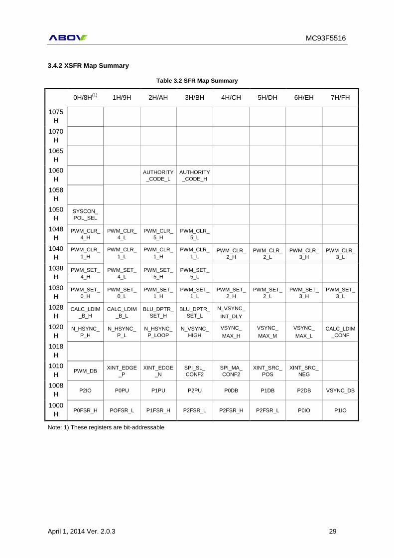
3.4.2 XSFR Map Summary
Table 3.2 SFR Map Summary
0H/8H
(1) 1H/9H 2H/AH 3H/BH 4H/CH 5H/DH 6H/EH 7H/FH
1075
H
1070
H
1065
H
1060
H
AUTHORITY
_CODE_L
AUTHORITY
_CODE_H
1058
H
1050
H SYSCON_
POL_SEL
1048
H PWM_CLR_
4_H
PWM_CLR_
4_L
PWM_CLR_
5_H
PWM_CLR_
5_L
1040
H
PWM_CLR_
1_H
PWM_CLR_
1_L
PWM_CLR_
1_H
PWM_CLR_
1_L PWM_CLR_
2_H
PWM_CLR_
2_L
PWM_CLR_
3_H
PWM_CLR_
3_L
1038
H PWM_SET_
4_H
PWM_SET_
4_L
PWM_SET_
5_H
PWM_SET_
5_L
1030
H PWM_SET_
0_H
PWM_SET_
0_L
PWM_SET_
1_H
PWM_SET_
1_L
PWM_SET_
2_H
PWM_SET_
2_L
PWM_SET_
3_H
PWM_SET_
3_L
1028
H CALC_LDIM
_B_H
CALC_LDIM
_B_L
BLU_DPTR_
SET_H
BLU_DPTR_
SET_L
N_VSYNC_
INT_DLY
1020
H N_HSYNC_
P_H
N_HSYNC_
P_L
N_HSYNC_
P_LOOP
N_VSYNC_
HIGH
VSYNC_
MAX_H
VSYNC_
MAX_M
VSYNC_
MAX_L
CALC_LDIM
_CONF
1018
H
1010
H PWM_DB
XINT_EDGE
_P
XINT_EDGE
_N
SPI_SL_
CONF2
SPI_MA_
CONF2
XINT_SRC_
POS
XINT_SRC_
NEG
1008
H P2IO P0PU P1PU P2PU P0DB P1DB P2DB VSYNC_DB
1000
H P0FSR_H POFSR_L P1FSR_H P2FSR_L P2FSR_H P2FSR_L P0IO P1IO
Note: 1) These registers are bit-addressable
MC93F5516
30 April 1, 2014 Ver. 2.0.3
3.4.3 Compiler Compatible SFR
ACC (Accumulator) : E0H
7 6 5 4 3 2 1 0
ACC
R/W R/W R/W R/W R/W R/W R/W R/W
Initial value : 00H
ACC Accumulator
B (B Register) : F0H
7 6 5 4 3 2 1 0
B
R/W R/W R/W R/W R/W R/W R/W R/W
Initial value : 00H
B B Register
SP (Stack Pointer) : 81H
7 6 5 4 3 2 1 0
SP
R/W R/W R/W R/W R/W R/W R/W R/W
Initial value : 07H
SP Stack Pointer
DPL (Data Pointer Low Byte) : 82H
7 6 5 4 3 2 1 0
DPL
R/W R/W R/W R/W R/W R/W R/W R/W
Initial value : 00H
DPL Data Pointer Low Byte
DPH (Data Pointer High Byte) : 83H
7 6 5 4 3 2 1 0
DPH
R/W R/W R/W R/W R/W R/W R/W R/W
Initial value : 00H
DPH Data Pointer High Byte
MC93F5516
April 1, 2014 Ver. 2.0.3 31
PSW (Program Status Word) : D0H
7 6 5 4 3 2 1 0
CY AC F0 RS1 RS0 OV F1 P
R/W R/W R/W R/W R/W R/W R/W R/W
Initial value : 00H
CY Carry Flag
AC Auxiliary Carry Flag
F0 General Purpose User-Definable Flag
RS1 Register Bank Select bit 1
Must be ‘0’.
RS0 Register Bank Select bit 0
Must be ‘0’.
OV Overflow Flag
F1 User-Definable Flag
P Parity Flag. Set/cleared by hardware each instruction cycle to indicate an odd/even number of ‘1’ bits in the accumulator
Note: MC93F5516 doesn’t support register bank selection. And RS[1:0] must be zero.
EO (Extended Operation Register) : A2H
7 6 5 4 3 2 1 0
- - - TRAP_EN 0 - - DPSEL0
- - - R/W R/W - - R/W
Initial value : 00H
TRAP_EN Select the instruction to be executed by opcode A5h as follows.
0 Select MOVC @(DPTR++), A
1 Select software TRAP instruction.
DPSEL[2:0] Data Pointer Select bits as follows:
000 DPTR0 selected
001 DPTR1 selected
MC93F5516
32 April 1, 2014 Ver. 2.0.3
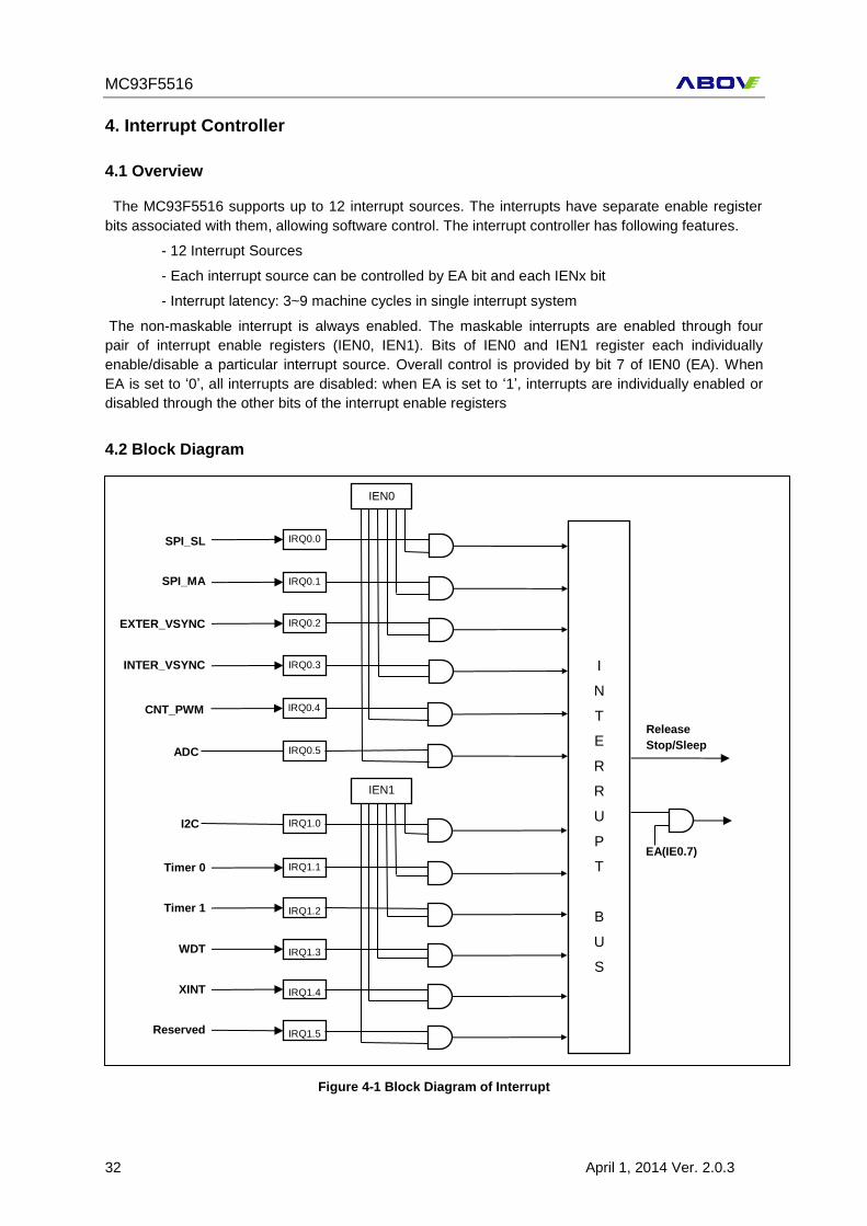
4. Interrupt Controller
4.1 Overview
The MC93F5516 supports up to 12 interrupt sources. The interrupts have separate enable register
bits associated with them, allowing software control. The interrupt controller has following features.
- 12 Interrupt Sources
- Each interrupt source can be controlled by EA bit and each IENx bit
- Interrupt latency: 3~9 machine cycles in single interrupt system
The non-maskable interrupt is always enabled. The maskable interrupts are enabled through four
pair of interrupt enable registers (IEN0, IEN1). Bits of IEN0 and IEN1 register each individually
enable/disable a particular interrupt source. Overall control is provided by bit 7 of IEN0 (EA). When
EA is set to ‘0’, all interrupts are disabled: when EA is set to ‘1’, interrupts are individually enabled or
disabled through the other bits of the interrupt enable registers
4.2 Block Diagram
Figure 4-1 Block Diagram of Interrupt
IRQ1.1
IRQ1.2
IRQ1.3
IRQ1.4
IRQ1.5
IEN0
I
N
T
E
R
R
U
P
T
B
U
S
Release
Stop/Sleep
IRQ0.3
EA(IE0.7)
Timer 0
Timer 1
WDT
XINT
Reserved
IRQ0.4 CNT_PWM
ADC IRQ0.5
IRQ0.0
IRQ0.1
IRQ0.2
IRQ1.0
IEN1
I2C
SPI_SL
SPI_MA
EXTER_VSYNC
INTER_VSYNC
MC93F5516
April 1, 2014 Ver. 2.0.3 33
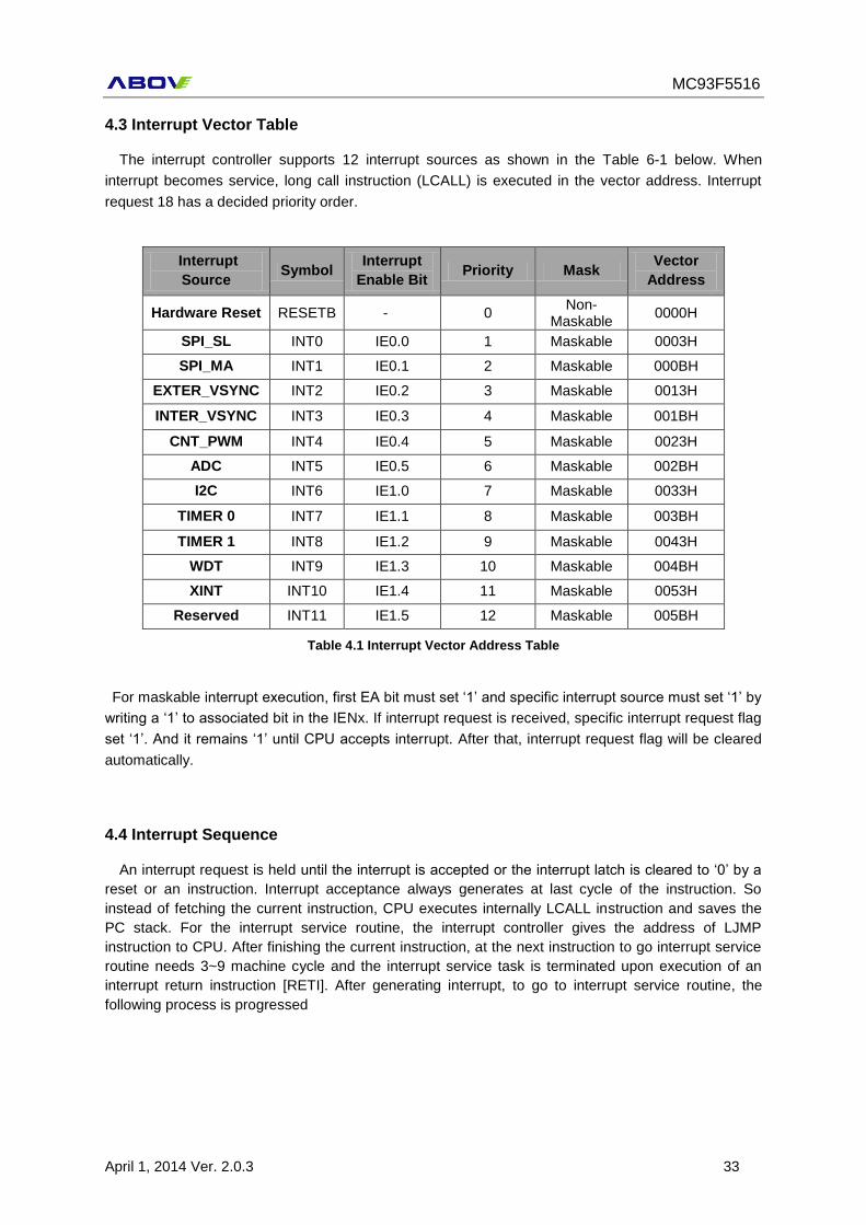
4.3 Interrupt Vector Table
The interrupt controller supports 12 interrupt sources as shown in the Table 6-1 below. When
interrupt becomes service, long call instruction (LCALL) is executed in the vector address. Interrupt
request 18 has a decided priority order.
Interrupt
Source Symbol
Interrupt
Enable Bit Priority Mask
Vector
Address
Hardware Reset RESETB - 0 Non-
Maskable 0000H
SPI_SL INT0 IE0.0 1 Maskable 0003H
SPI_MA INT1 IE0.1 2 Maskable 000BH
EXTER_VSYNC INT2 IE0.2 3 Maskable 0013H
INTER_VSYNC INT3 IE0.3 4 Maskable 001BH
CNT_PWM INT4 IE0.4 5 Maskable 0023H
ADC INT5 IE0.5 6 Maskable 002BH
I2C INT6 IE1.0 7 Maskable 0033H
TIMER 0 INT7 IE1.1 8 Maskable 003BH
TIMER 1 INT8 IE1.2 9 Maskable 0043H
WDT INT9 IE1.3 10 Maskable 004BH
XINT INT10 IE1.4 11 Maskable 0053H
Reserved INT11 IE1.5 12 Maskable 005BH
Table 4.1 Interrupt Vector Address Table
For maskable interrupt execution, first EA bit must set ‘1’ and specific interrupt source must set ‘1’ by
writing a ‘1’ to associated bit in the IENx. If interrupt request is received, specific interrupt request flag
set ‘1’. And it remains ‘1’ until CPU accepts interrupt. After that, interrupt request flag will be cleared
automatically.
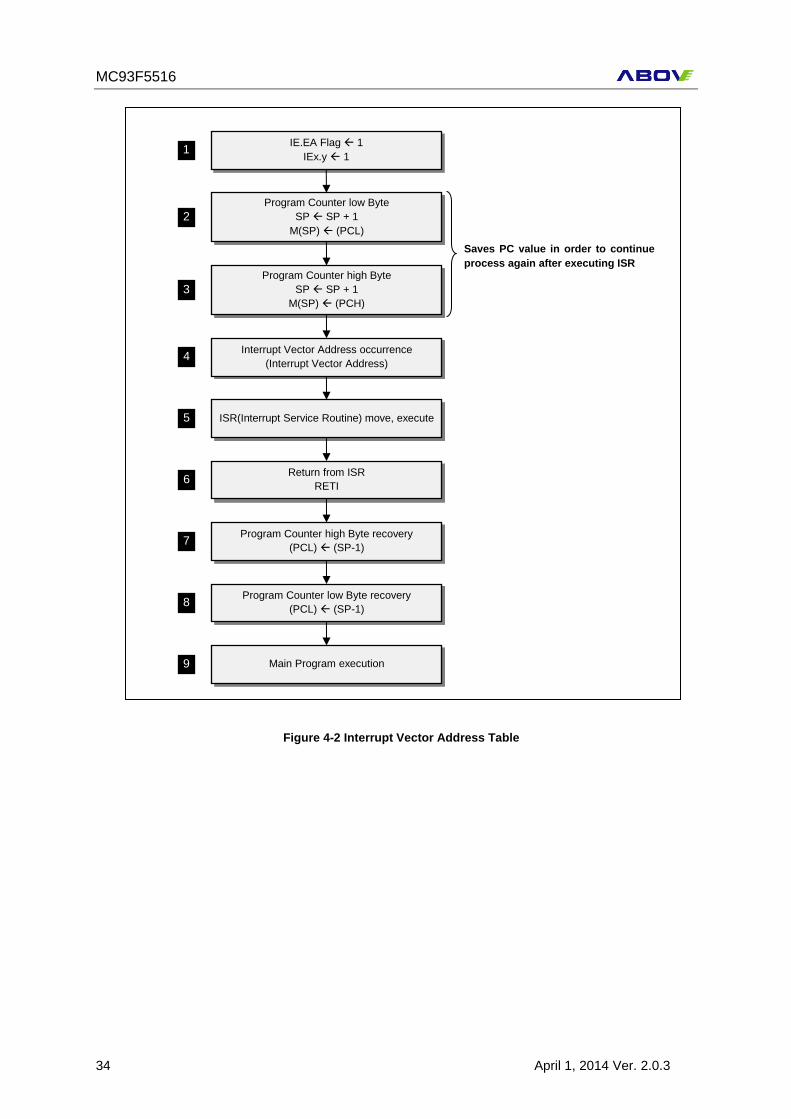
4.4 Interrupt Sequence
An interrupt request is held until the interrupt is accepted or the interrupt latch is cleared to ‘0’ by a
reset or an instruction. Interrupt acceptance always generates at last cycle of the instruction. So
instead of fetching the current instruction, CPU executes internally LCALL instruction and saves the
PC stack. For the interrupt service routine, the interrupt controller gives the address of LJMP
instruction to CPU. After finishing the current instruction, at the next instruction to go interrupt service
routine needs 3~9 machine cycle and the interrupt service task is terminated upon execution of an
interrupt return instruction [RETI]. After generating interrupt, to go to interrupt service routine, the
following process is progressed
MC93F5516
34 April 1, 2014 Ver. 2.0.3
Saves PC value in order to continue
process again after executing ISR
IE.EA Flag 1
IEx.y 1 1
Program Counter low Byte
SP SP + 1
M(SP) (PCL)
2
Program Counter high Byte
SP SP + 1
M(SP) (PCH)
3
Interrupt Vector Address occurrence
(Interrupt Vector Address) 4
ISR(Interrupt Service Routine) move, execute 5
Return from ISR
RETI 6
Program Counter high Byte recovery
(PCL) (SP-1) 7
Main Program execution 9
Program Counter low Byte recovery
(PCL) (SP-1) 8
Figure 4-2 Interrupt Vector Address Table
MC93F5516
April 1, 2014 Ver. 2.0.3 35
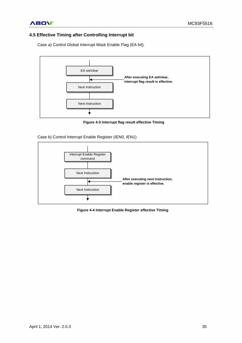
4.5 Effective Timing after Controlling Interrupt bit
Case a) Control Global Interrupt Mask Enable Flag (EA bit).
Case b) Control Interrupt Enable Register (IEN0, IEN1)
Interrupt Enable Register
command
Next Instruction
Next Instruction
After executing next instruction,
enable register is effective.
Figure 4-3 Interrupt flag result effective Timing
Figure 4-4 Interrupt Enable Register effective Timing
EA set/clear
Next Instruction
Next Instruction
After executing EA set/clear,
interrupt flag result is effective.
MC93F5516
36 April 1, 2014 Ver. 2.0.3
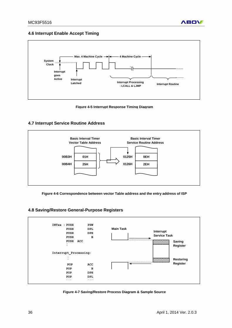
4.6 Interrupt Enable Accept Timing
4.7 Interrupt Service Routine Address
4.8 Saving/Restore General-Purpose Registers
Interrupt
Latched
Interrupt
goes
Active
System
Clock
Max. 4 Machine Cycle 4 Machine Cycle
Interrupt Processing
: LCALL & LJMP Interrupt Routine
Figure 4-5 Interrupt Response Timing Diagram
01H
25H
00B3H
00B4H
Basic Interval Timer
Vector Table Address
0EH
2EH
0125H
0126H
Basic Interval Timer
Service Routine Address
Figure 4-6 Correspondence between vector Table address and the entry address of ISP
Main Task
Saving
Register
Restoring
Register
Interrupt
Service Task
INTxx : PUSH PSW
PUSH DPL
PUSH DPH
PUSH B
PUSH ACC ∙ ∙
Interrupt_Processing:
∙ ∙
POP ACC
POP B
POP DPH
POP DPL
POP PSW
Figure 4-7 Saving/Restore Process Diagram & Sample Source
MC93F5516
April 1, 2014 Ver. 2.0.3 37
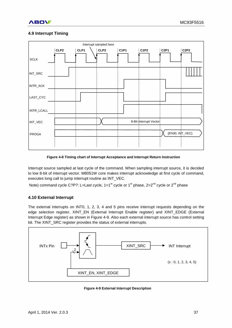
4.9 Interrupt Timing
Interrupt source sampled at last cycle of the command. When sampling interrupt source, it is decided
to low 8-bit of interrupt vector. M8051W core makes interrupt acknowledge at first cycle of command,
executes long call to jump interrupt routine as INT_VEC.
Note) command cycle C?P?: L=Last cycle, 1=1st cycle or 1
st phase, 2=2
nd cycle or 2
nd phase
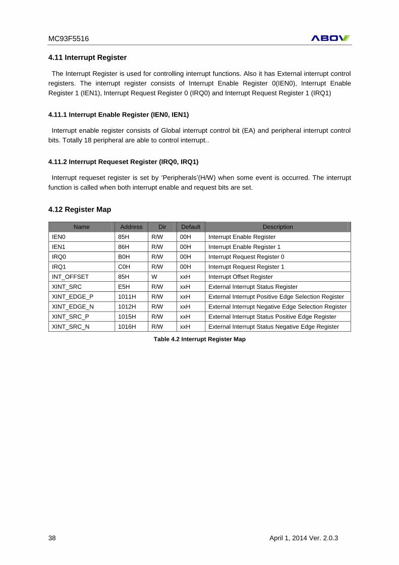
4.10 External Interrupt
The external interrupts on INT0, 1, 2, 3, 4 and 5 pins receive interrupt requests depending on the
edge selection register, XINT_EN (External Interrupt Enable register) and XINT_EDGE (External
Interrupt Edge register) as shown in Figure 4-9. Also each external interrupt source has control setting
bit. The XINT_SRC register provides the status of external interrupts.
Figure 4-9 External Interrupt Description
CLP2 CLP1 C2P1 C1P1 C2P2 C1P2 CLP2
Interrupt sampled here
8-Bit interrupt Vector
INT_SRC
INTR_ACK
LAST_CYC
INTR_LCALL
INT_VEC
PROGA
SCLK
8’h00, INT_VEC
INTx Pin XINT_SRC INT Interrupt
XINT_EN, XINT_EDGE
2
(x : 0, 1, 2, 3, 4, 5)
Figure 4-8 Timing chart of Interrupt Acceptance and Interrupt Return Instruction
MC93F5516
38 April 1, 2014 Ver. 2.0.3
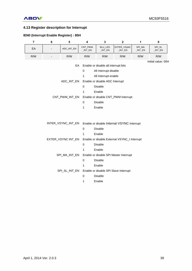
4.11 Interrupt Register
The Interrupt Register is used for controlling interrupt functions. Also it has External interrupt control
registers. The interrupt register consists of Interrupt Enable Register 0(IEN0), Interrupt Enable
Register 1 (IEN1), Interrupt Request Register 0 (IRQ0) and Interrupt Request Register 1 (IRQ1)
4.11.1 Interrupt Enable Register (IEN0, IEN1)
Interrupt enable register consists of Global interrupt control bit (EA) and peripheral interrupt control
bits. Totally 18 peripheral are able to control interrupt..
4.11.2 Interrupt Requeset Register (IRQ0, IRQ1)
Interrupt requeset register is set by ‘Peripherals’(H/W) when some event is occurred. The interrupt
function is called when both interrupt enable and request bits are set.
4.12 Register Map
Name Address Dir Default Description
IEN0 85H R/W 00H Interrupt Enable Register
IEN1 86H R/W 00H Interrupt Enable Register 1
IRQ0 B0H R/W 00H Interrupt Request Register 0
IRQ1 C0H R/W 00H Interrupt Request Register 1
INT_OFFSET 85H W xxH Interrupt Offset Register
XINT_SRC E5H R/W xxH External Interrupt Status Register
XINT_EDGE_P 1011H R/W xxH External Interrupt Positive Edge Selection Register
XINT_EDGE_N 1012H R/W xxH External Interrupt Negative Edge Selection Register
XINT_SRC_P 1015H R/W xxH External Interrupt Status Positive Edge Register
XINT_SRC_N 1016H R/W xxH External Interrupt Status Negative Edge Register
Table 4.2 Interrupt Register Map
MC93F5516
April 1, 2014 Ver. 2.0.3 39
4.13 Register description for Interrupt
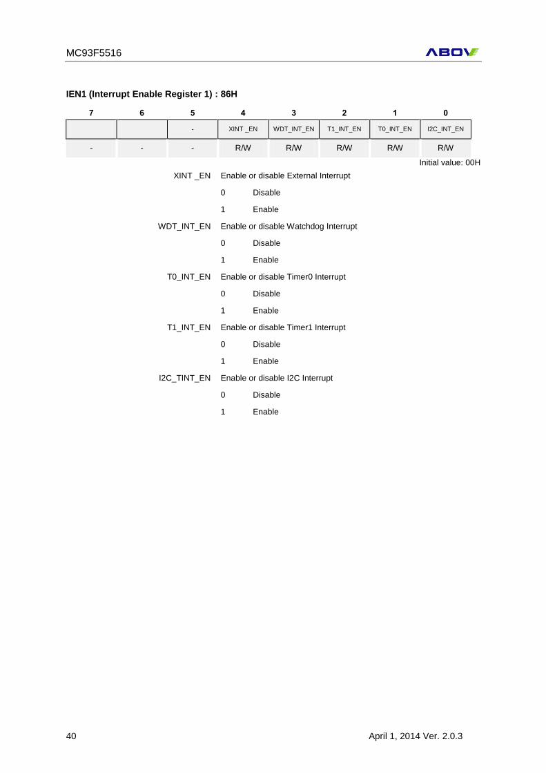
IEN0 (Interrupt Enable Register) : 85H
7 6 5 4 3 2 1 0
EA - ADC_INT_EN CNT_PWM
_INT_EN
BLU_LED
_INT_EN
EXTER_VSyNC
_INT_EN
SPI_MA
_INT_EN
SPI_SL
_INT_EN
R/W - R/W R/W R/W R/W R/W R/W
Initial value: 00H
EA Enable or disable all interrupt bits
0 All Interrupt disable
1 All Interrupt enable
ADC_INT_EN Enable or disable ADC Interrupt
0 Disable
1 Enable
CNT_PWM_INT_EN Enable or disable CNT_PWM Interrupt
0 Disable
1 Enable
INTER_VSYNC_INT_EN Enable or disable Internal VSYNC Interrupt
0 Disable
1 Enable
EXTER_VSYNC INT_EN Enable or disable External VSYNC_I Interrupt
0 Disable
1 Enable
SPI_MA_INT_EN Enable or disable SPI Master Interrupt
0 Disable
1 Enable
SPI_SL_INT_EN Enable or disable SPI Slave Interrupt
0 Disable
1 Enable
MC93F5516
40 April 1, 2014 Ver. 2.0.3
IEN1 (Interrupt Enable Register 1) : 86H
7 6 5 4 3 2 1 0
- XINT _EN WDT_INT_EN T1_INT_EN T0_INT_EN I2C_INT_EN
- - - R/W R/W R/W R/W R/W
Initial value: 00H
XINT _EN Enable or disable External Interrupt
0 Disable
1 Enable
WDT_INT_EN Enable or disable Watchdog Interrupt
0 Disable
1 Enable
T0_INT_EN Enable or disable Timer0 Interrupt
0 Disable
1 Enable
T1_INT_EN Enable or disable Timer1 Interrupt
0 Disable
1 Enable
I2C_TINT_EN Enable or disable I2C Interrupt
0 Disable
1 Enable
MC93F5516
April 1, 2014 Ver. 2.0.3 41
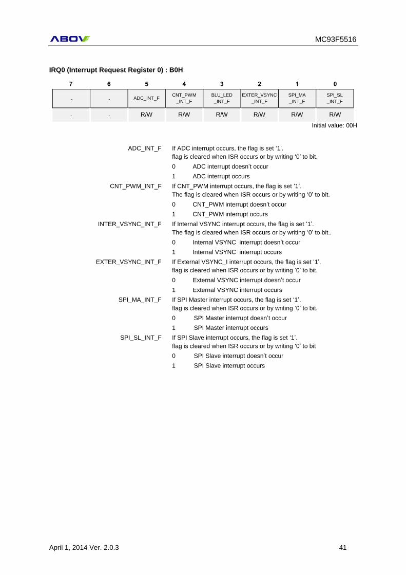
IRQ0 (Interrupt Request Register 0) : B0H
7 6 5 4 3 2 1 0
- - ADC_INT_F CNT_PWM
_INT_F
BLU_LED
_INT_F
EXTER_VSYNC
_INT_F
SPI_MA
_INT_F
SPI_SL
_INT_F
- - R/W R/W R/W R/W R/W R/W
Initial value: 00H
ADC_INT_F If ADC interrupt occurs, the flag is set ‘1’.
flag is cleared when ISR occurs or by writing ‘0’ to bit.
0 ADC interrupt doesn’t occur
1 ADC interrupt occurs
CNT_PWM_INT_F If CNT_PWM interrupt occurs, the flag is set ‘1’.
The flag is cleared when ISR occurs or by writing ‘0’ to bit.
0 CNT_PWM interrupt doesn’t occur
1 CNT_PWM interrupt occurs
INTER_VSYNC_INT_F If Internal VSYNC interrupt occurs, the flag is set ‘1’.
The flag is cleared when ISR occurs or by writing ‘0’ to bit..
0 Internal VSYNC interrupt doesn’t occur
1 Internal VSYNC interrupt occurs
EXTER_VSYNC_INT_F If External VSYNC_I interrupt occurs, the flag is set ‘1’.
flag is cleared when ISR occurs or by writing ‘0’ to bit.
0 External VSYNC interrupt doesn’t occur
1 External VSYNC interrupt occurs
SPI_MA_INT_F If SPI Master interrupt occurs, the flag is set ‘1’.
flag is cleared when ISR occurs or by writing ‘0’ to bit.
0 SPI Master interrupt doesn’t occur
1 SPI Master interrupt occurs
SPI_SL_INT_F If SPI Slave interrupt occurs, the flag is set ‘1’.
flag is cleared when ISR occurs or by writing ‘0’ to bit
0 SPI Slave interrupt doesn’t occur
1 SPI Slave interrupt occurs

MC93F5516
42 April 1, 2014 Ver. 2.0.3
IRQ1 (Interrupt Request Register 1) : C0H
7 6 5 4 3 2 1 0
- - XINT_F WDT_INT_F T1_INT_F T0_INT_F I2C_INT_F
- - R/W R/W R/W R/W R/W
Initial value: 00H
XINT_F If External interrupt occurs, the flag is set ‘1’.
flag is cleared when ISR occurs or by writing ‘0’ to bit.
0 External interrupt doesn’t occur
1 External interrupt occurs
WDT_INT_F If Watchdog Timer interrupt occurs, the flag is set ‘1’.
flag is cleared when ISR occurs or by writing ‘0’ to bit.
0 Watchdog Timer interrupt doesn’t occur
1 Watchdog Timer interrupt occurs
T1_INT_F If Timer2 interrupt occurs, the flag is set ‘1’.
flag is cleared when ISR occurs or by writing ‘0’ to bit.
0 Timer1 interrupt doesn’t occur
1 Timer1 interrupt occurs
T0_INT_F If Timer1 interrupt occurs, the flag is set ‘1’.
The flag is cleared when ISR occurs or by writing ‘0’ to bit.
0 Timer0 interrupt doesn’t occur
1 Timer0 interrupt occurs
I2C_INT_F If Timer 0 interrupt occurs, the flag is set ‘1’.
flag is cleared when ISR occurs or by writing ‘0’ to bit.
0 I2C interrupt doesn’t occur
1 I2C interrupt occurs
INT_OFFET (Interrupt Offset Register) : 85H
7 6 5 4 3 2 1 0
OFFSET7 OFFSET6 OFFSET5 OFFSET4 OFFSET3 OFFSET2 OFFSET1 OFFSET0
W W W- W W W W W
Initial value : xxH
OFFSET[7:0] Interrupt Offset Value
Interrupt Vector Address = 256*INT_OFFSET
Interrupt Offset changing is possible when only the SYSCON_AR v
alue is 5Ah. So user must set it with 5Ah before chang
ing interrupt offset value and make sure set it with 00h after
changing interrupt offset.
XINT_SRC (External Interrupt Status Register) : E5H
7 6 5 4 3 2 1 0
- - XINT5_ F XINT4_ F XINT3_ F XINT2_ F XINT1_F XINT0_ F
- - R/W R/W R/W R/W R/W R/W
Initial value : xxH
XINTn_ F If External interrupt occurs, the flag is set ‘1’.
flag is cleared by writing ‘0’ to bit.
0 External interrupt doesn’t occur.
1 External interrupt occurs.
MC93F5516
April 1, 2014 Ver. 2.0.3 43
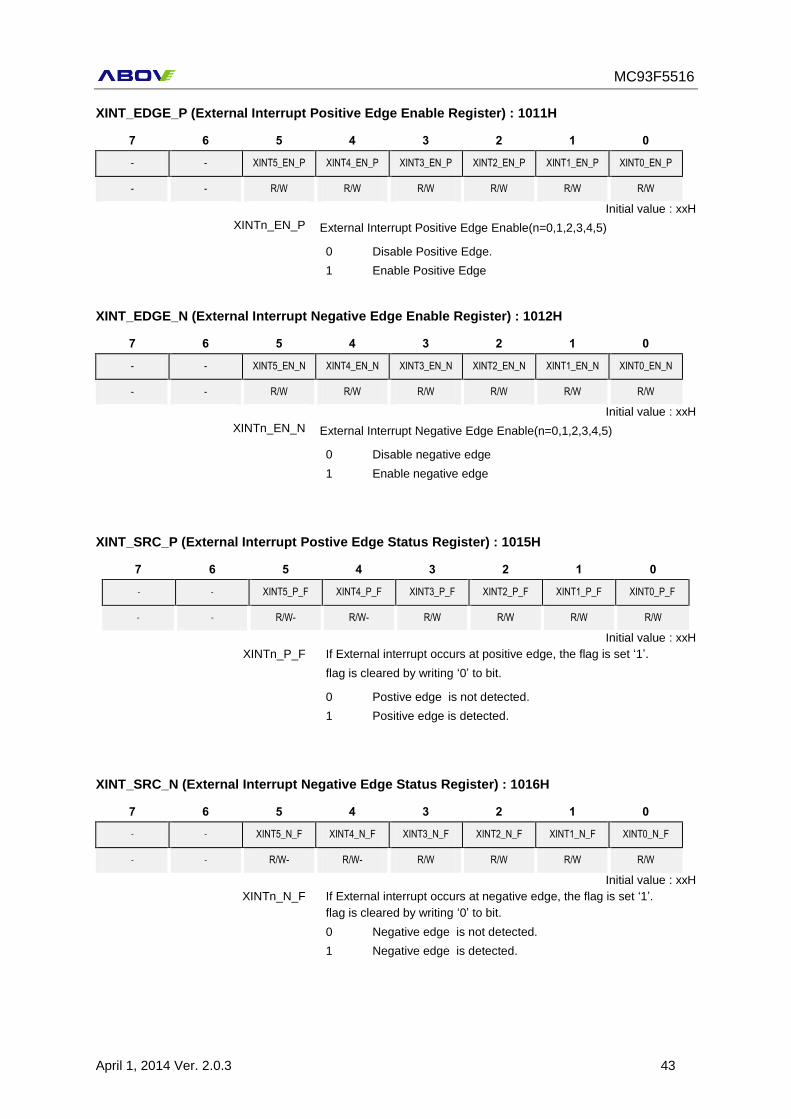
XINT_EDGE_P (External Interrupt Positive Edge Enable Register) : 1011H
7 6 5 4 3 2 1 0
- - XINT5_EN_P XINT4_EN_P XINT3_EN_P XINT2_EN_P XINT1_EN_P XINT0_EN_P
- - R/W R/W R/W R/W R/W R/W
Initial value : xxH
XINTn_EN_P External Interrupt Positive Edge Enable(n=0,1,2,3,4,5)
0 Disable Positive Edge.
1 Enable Positive Edge
XINT_EDGE_N (External Interrupt Negative Edge Enable Register) : 1012H
7 6 5 4 3 2 1 0
- - XINT5_EN_N XINT4_EN_N XINT3_EN_N XINT2_EN_N XINT1_EN_N XINT0_EN_N
- - R/W R/W R/W R/W R/W R/W
Initial value : xxH
XINTn_EN_N External Interrupt Negative Edge Enable(n=0,1,2,3,4,5)
0 Disable negative edge
1 Enable negative edge
XINT_SRC_P (External Interrupt Postive Edge Status Register) : 1015H
7 6 5 4 3 2 1 0
- - XINT5_P_F XINT4_P_F XINT3_P_F XINT2_P_F XINT1_P_F XINT0_P_F
- - R/W- R/W- R/W R/W R/W R/W
Initial value : xxH
XINTn_P_F If External interrupt occurs at positive edge, the flag is set ‘1’.
flag is cleared by writing ‘0’ to bit.
0 Postive edge is not detected.
1 Positive edge is detected.
XINT_SRC_N (External Interrupt Negative Edge Status Register) : 1016H
7 6 5 4 3 2 1 0
- - XINT5_N_F XINT4_N_F XINT3_N_F XINT2_N_F XINT1_N_F XINT0_N_F
- - R/W- R/W- R/W R/W R/W R/W
Initial value : xxH
XINTn_N_F If External interrupt occurs at negative edge, the flag is set ‘1’.
flag is cleared by writing ‘0’ to bit.
0 Negative edge is not detected.
1 Negative edge is detected.
MC93F5516
44 April 1, 2014 Ver. 2.0.3
5. Clock Control and Power Saving
5.1 Clock Generator
5.1.1 Overview
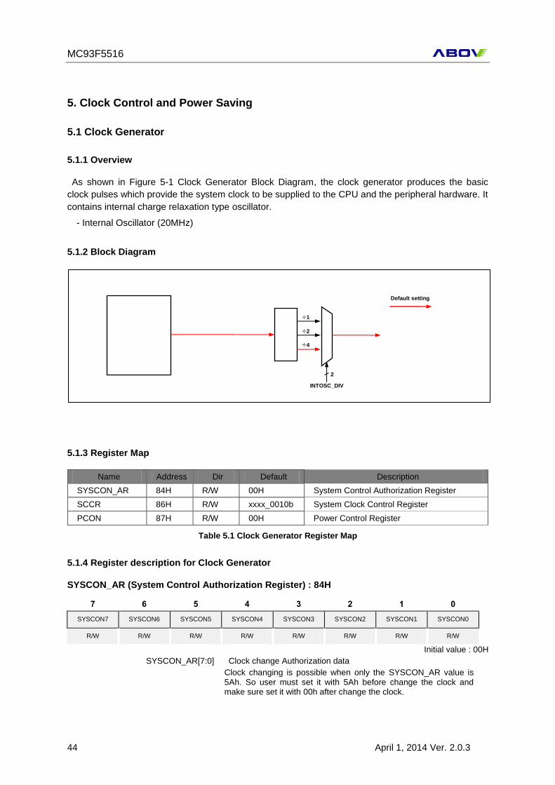
As shown in Figure 5-1 Clock Generator Block Diagram, the clock generator produces the basic
clock pulses which provide the system clock to be supplied to the CPU and the peripheral hardware. It
contains internal charge relaxation type oscillator.
- Internal Oscillator (20MHz)
5.1.2 Block Diagram
5.1.3 Register Map
Name Address Dir Default Description
SYSCON_AR 84H R/W 00H System Control Authorization Register
SCCR 86H R/W xxxx_0010b System Clock Control Register
PCON 87H R/W 00H Power Control Register
Table 5.1 Clock Generator Register Map
5.1.4 Register description for Clock Generator
SYSCON_AR (System Control Authorization Register) : 84H
7 6 5 4 3 2 1 0
SYSCON7 SYSCON6 SYSCON5 SYSCON4 SYSCON3 SYSCON2 SYSCON1 SYSCON0
R/W R/W R/W R/W R/W R/W R/W R/W
Initial value : 00H
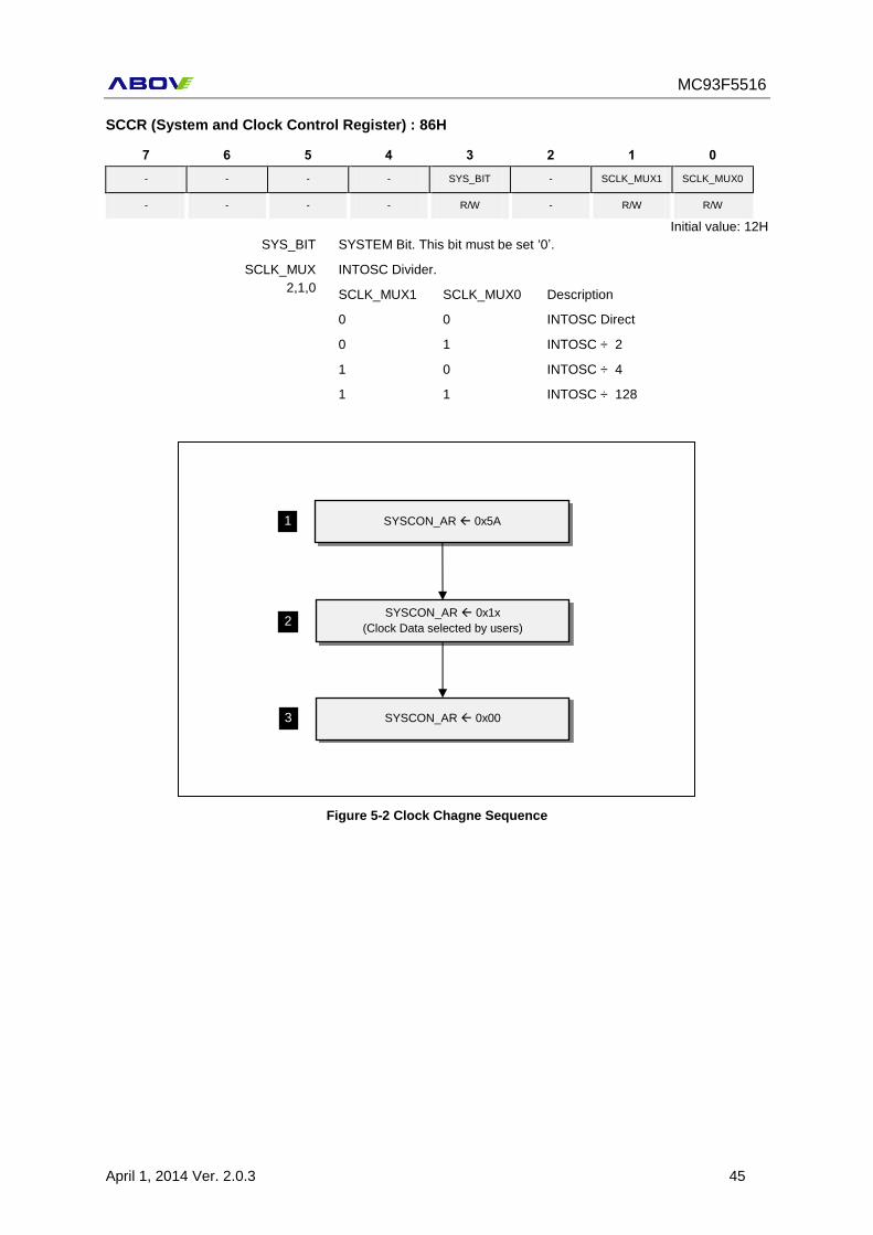
SYSCON_AR[7:0] Clock change Authorization data
Clock changing is possible when only the SYSCON_AR value is 5Ah. So user must set it with 5Ah before change the clock and make sure set it with 00h after change the clock.
Figure 5-1 Clock Generator Block Diagram
÷1
÷2
÷4
INTOSC_DIV
2
Default setting
MC93F5516
April 1, 2014 Ver. 2.0.3 45
SCCR (System and Clock Control Register) : 86H
7 6 5 4 3 2 1 0
- - - - SYS_BIT - SCLK_MUX1 SCLK_MUX0
- - - - R/W - R/W R/W
Initial value: 12H
SYS_BIT SYSTEM Bit. This bit must be set ‘0’.
SCLK_MUX
2,1,0
INTOSC Divider.
SCLK_MUX1 SCLK_MUX0 Description
0 0 INTOSC Direct
0 1 INTOSC ÷ 2
1 0 INTOSC ÷ 4
1 1 INTOSC ÷ 128
Figure 5-2 Clock Chagne Sequence
SYSCON_AR 0x5A 1
2 SYSCON_AR 0x1x
(Clock Data selected by users)
3 SYSCON_AR 0x00
MC93F5516
46 April 1, 2014 Ver. 2.0.3
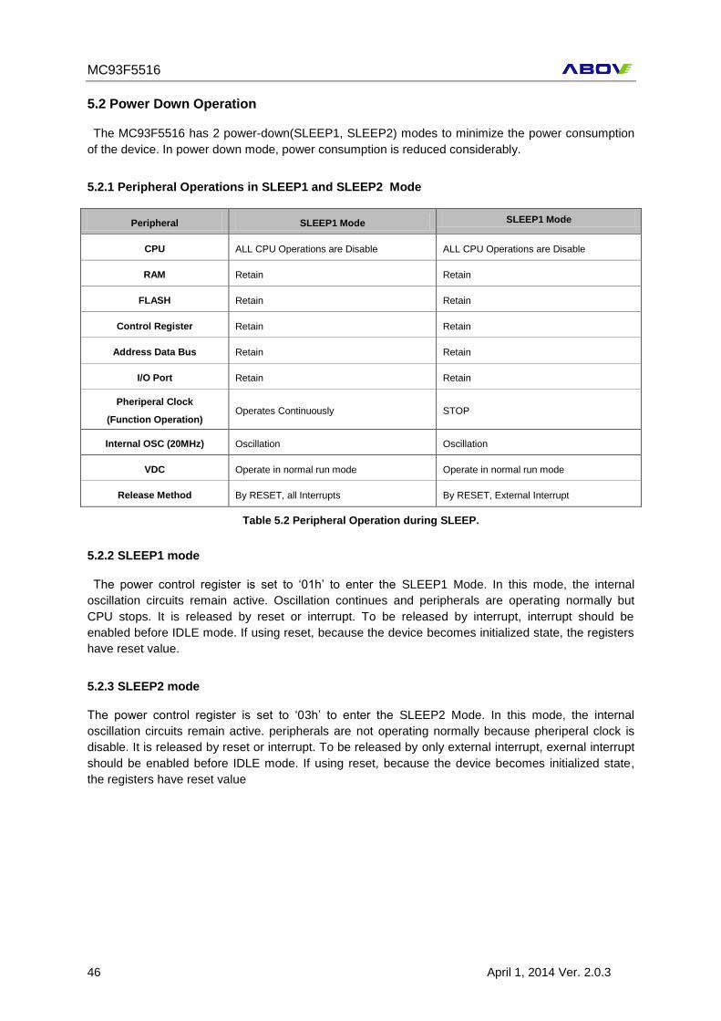
5.2 Power Down Operation
The MC93F5516 has 2 power-down(SLEEP1, SLEEP2) modes to minimize the power consumption
of the device. In power down mode, power consumption is reduced considerably.
5.2.1 Peripheral Operations in SLEEP1 and SLEEP2 Mode
Peripheral SLEEP1 Mode SLEEP1 Mode
CPU ALL CPU Operations are Disable ALL CPU Operations are Disable
RAM Retain Retain
FLASH Retain Retain
Control Register Retain Retain
Address Data Bus Retain Retain
I/O Port Retain Retain
Pheriperal Clock
(Function Operation) Operates Continuously STOP
Internal OSC (20MHz) Oscillation Oscillation
VDC Operate in normal run mode Operate in normal run mode
Release Method By RESET, all Interrupts By RESET, External Interrupt
Table 5.2 Peripheral Operation during SLEEP.
5.2.2 SLEEP1 mode
The power control register is set to ‘01h’ to enter the SLEEP1 Mode. In this mode, the internal
oscillation circuits remain active. Oscillation continues and peripherals are operating normally but
CPU stops. It is released by reset or interrupt. To be released by interrupt, interrupt should be
enabled before IDLE mode. If using reset, because the device becomes initialized state, the registers
have reset value.
5.2.3 SLEEP2 mode
The power control register is set to ‘03h’ to enter the SLEEP2 Mode. In this mode, the internal
oscillation circuits remain active. peripherals are not operating normally because pheriperal clock is
disable. It is released by reset or interrupt. To be released by only external interrupt, exernal interrupt
should be enabled before IDLE mode. If using reset, because the device becomes initialized state,
the registers have reset value
MC93F5516
April 1, 2014 Ver. 2.0.3 47
5.2.4 Register Map
Name Address Dir Default Description
PCON 87H R/W 00H Power Control Register
Table 5.3 PCON Register Map
5.2.5 Register description for Power Down Operation
PCON (Power Control Register) : 87H
7 6 5 4 3 2 1 0
POWER_MODE7 POWER_MODE6 POWER_MODE5 POWER_MODE4 POWER_MODE3 POWER_MODE2 POWER_MODE1 POWER_MODE
R/W R/W R/W R/W R/W R/W R/W R/W
Initial value : 00H
POWER_MODE Power Mode Selection
00H Normal Mode enable
01H SLEEP1 Mode enable
03H SLEEP2 Mode enable
The Power Down Operation Register consists of the Power Control Register (PCON).
To enter SLEEP1 Mode, PCON must be set to ‘01H’.
To enter SLEEP2 Mode, PCON must be set to ‘03H’.
(In STOP2 Mode, PCON register is cleared automatically by interrupt or reset)
Figure 5-3 SLEEP1, 2 Mode Release Timing by External Interrupt
External
Interrupt
Normal Operation
Release
CPU Clock
Stand-by Mode Normal Operation
OSC

MC93F5516
48 April 1, 2014 Ver. 2.0.3
6. RESET
6.1 Overview
When the RESET event is occured, internal registers are initialized by following table.
Table 6-1 Reset State
On Chip Hardware Reset Value
Program Counter(PC) 0x0000
Accumulator 0x00
Stack Pointer 0x07
SCCR 0x20(5MHz)
SYSCON_AR 0x00(clock change disable)
6.2 Reset Source
MC93F5516UB has three types of reset generation procedures. All reset sources are listed below.
- Power On RESET(POR)
- WDT RESET
- OCD RESET
Figure 6-1 RESET Block Diagram
6.3 Reset Procedure
When all of RESETB source signals are released to HIGH after at least one of them are holding LOW,
‘RESETB’ signal is released HIGH. After ‘RESETB’ signal is relased to HIGH, stabilization time is
counted by 16 bit timer and ‘System RESETB’ signal is released after stabilization time. After then
user code is excuted from address 0x0000.
The stabilization time is counted by system clock and the system clock configuration is initialized by
POR reset. Therefor the system clock is always 5MHz and the stabilization time is always around
13.1ms when POR reset situation. In other reset situation like external, WDT and OCD reset, the
system clock can be changed by user code. Therefor the stabilization time can be changed based on
the selected system clock configuration. The stabilization time is one period time of 16 bit counter by
system clock. For example when the system clock is configured by 16MHz, the stabilization time is
around 3.27ms.
After the system clock is counted until 63488 counts, trimming values are updated when only POR
reset situation. In other reset situations the trimming values are not updated. All trimming values
(listed bellow) are updated by recorded values in the configuration area at the update timing.
- OSC. trimming value
- VDC trimming value
POR RESETB WDT RESETB OCD RESETB
RESETB

MC93F5516
April 1, 2014 Ver. 2.0.3 49
6.4 Power On Reset
The POR(Power On Reset) have as function to reset the device when the VDD is rising. When VDD is
over VPOR(2.2V typical), ‘POR RESETB’ signal is released HIGH and when VDD is under VPOR, ‘POR
RESETB’ signal is hoding LOW. Therefor, MCU is running when only VDD is over VPOR.
RESETB
(Internal Signal)
System RESETB
Internal Oscillation
(20MHz)
RESET TIMER Starts
RESET TIMER Overflows
System Clock
(5MHz)
Stabilization time = 65536 * 200ns ≈ 13.1ms (always 5MHz sys. clock)
Triming values update timing = 63488 * 200ns ≈ 12.7ms
Trimming Value Read
POR RESET
situation
Stabilization time = 65536 * SCKKT ≈ 3.27ms (When 20MHz sys. clock)
Triming values are not updated Other RESET
situations
VDD
(POR) RESETB
(Internal Signal)
System RESETB
RESET TIMER
Starts
RESET TIMER
Overflows
VPOR=2.2V (Typ)
RESET TIMER
Starts
Figure 6-3 POR Reset Diagram
Figure 6-2 RESET Timing Diagram
MC93F5516
50 April 1, 2014 Ver. 2.0.3
7. Peripherals
7.1 Watch Dog Timer
7.1.1 Overview
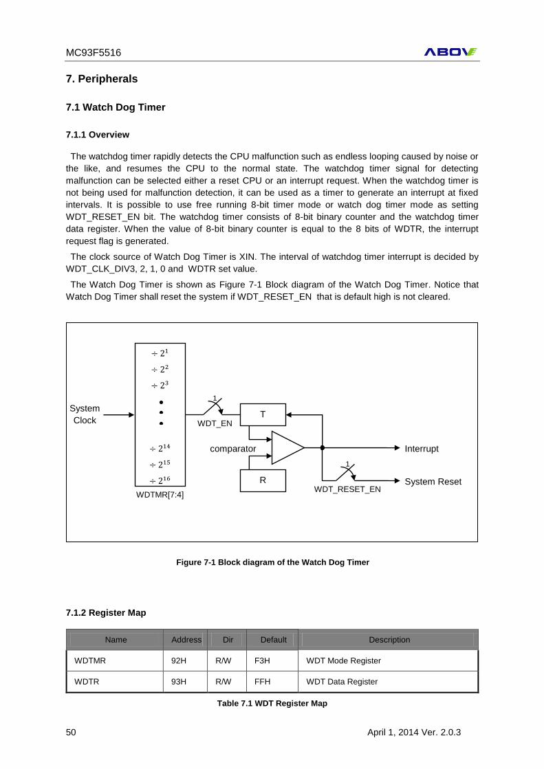
The watchdog timer rapidly detects the CPU malfunction such as endless looping caused by noise or
the like, and resumes the CPU to the normal state. The watchdog timer signal for detecting
malfunction can be selected either a reset CPU or an interrupt request. When the watchdog timer is
not being used for malfunction detection, it can be used as a timer to generate an interrupt at fixed
intervals. It is possible to use free running 8-bit timer mode or watch dog timer mode as setting
WDT_RESET_EN bit. The watchdog timer consists of 8-bit binary counter and the watchdog timer
data register. When the value of 8-bit binary counter is equal to the 8 bits of WDTR, the interrupt
request flag is generated.
The clock source of Watch Dog Timer is XIN. The interval of watchdog timer interrupt is decided by
WDT_CLK_DIV3, 2, 1, 0 and WDTR set value.
The Watch Dog Timer is shown as Figure 7-1 Block diagram of the Watch Dog Timer. Notice that
Watch Dog Timer shall reset the system if WDT_RESET_EN that is default high is not cleared.
7.1.2 Register Map
Name Address Dir Default Description
WDTMR 92H R/W F3H WDT Mode Register
WDTR 93H R/W FFH WDT Data Register
Table 7.1 WDT Register Map
÷ 21
÷ 22
÷ 23
÷ 214
÷ 215
÷ 216
WDTMR[7:4]
System
Clock WDT_EN T
R
comparator
WDT_RESET_EN
1
1
Interrupt
System Reset
Figure 7-1 Block diagram of the Watch Dog Timer
MC93F5516
April 1, 2014 Ver. 2.0.3 51
7.1.3 Register description for Watch Dog Timer
WDTMR (Watch Dog Timer Mode Register) : 92H
7 6 5 4 3 2 1 0
WDT_CLK_DIV3 WDT_CLK_DIV2 WDT_CLK_DIV1 WDT_CLK_DIV0 - WDT_CLR WDT_RESET_EN WDT_EN
R/W R/W R/W R/W - W R/W R/W
Initial value: F3H
WDT_CLK_DIV 3,2,1,0
WDT Clock Divider
DIV3 DIV2 DIV1 DIV0 Description
0 0 0 0 System Clock ÷ 20
0 0 0 1 System Clock ÷ 21
0 0 1 0 System Clock ÷ 22
0 0 1 1 System Clock ÷ 23
0 1 0 0 System Clock ÷ 24
0 1 0 1 System Clock ÷ 25
0 1 1 0 System Clock ÷ 26
0 1 1 1 System Clock ÷ 27
1 0 0 0 System Clock ÷ 28
1 0 0 1 System Clock ÷ 29
1 0 1 0 System Clock ÷ 210
1 0 1 1 System Clock ÷ 211
1 1 0 0 System Clock ÷ 212
1 1 0 1 System Clock ÷ 213
1 1 1 0 System Clock ÷ 214
1 1 1 1 System Clock ÷ 215
WDT_CLR Clear WDT Counter
0 Free Run
1 Clear WDT Counter (auto clear after 1 Cycle)
WDT_RESET_EN WDT Reset Enable bit
0 Reset Disable
1 Reset Enable
WDT_EN WDT Enable bit
0 WDT disable
1 WDT Enable
WDTR (Watch Dog Timer Register: Write Case) : 93H
7 6 5 4 3 2 1 0
WDTR7 WDTR6 WDTR5 WDTR4 WDTR3 WDTR2 WDTR1 WDTR0
W W W W W W W W
Initial value: FFH
WDTR[7:0] Set a period
WDT Interrupt Interval=(System Clock / WDT_CLK_DIV) x(WDTR Value+1)
Note) To guarantee proper operation, the data should be greater than 01H.
MC93F5516
52 April 1, 2014 Ver. 2.0.3
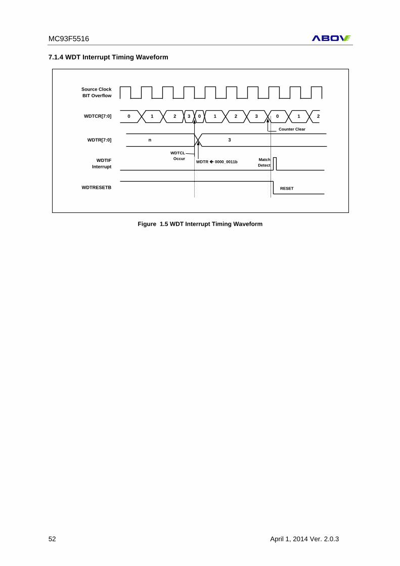
7.1.4 WDT Interrupt Timing Waveform
Source Clock
BIT Overflow
WDTCR[7:0]
WDTR[7:0]
WDTIF
Interrupt
WDTRESETB
WDTCL
Occur WDTR 0000_0011b
Match
Detect
Counter Clear
RESET
0 1 2 3 0 1 2 3 0 1 2
n 3
Figure 1.5 WDT Interrupt Timing Waveform
MC93F5516
April 1, 2014 Ver. 2.0.3 53
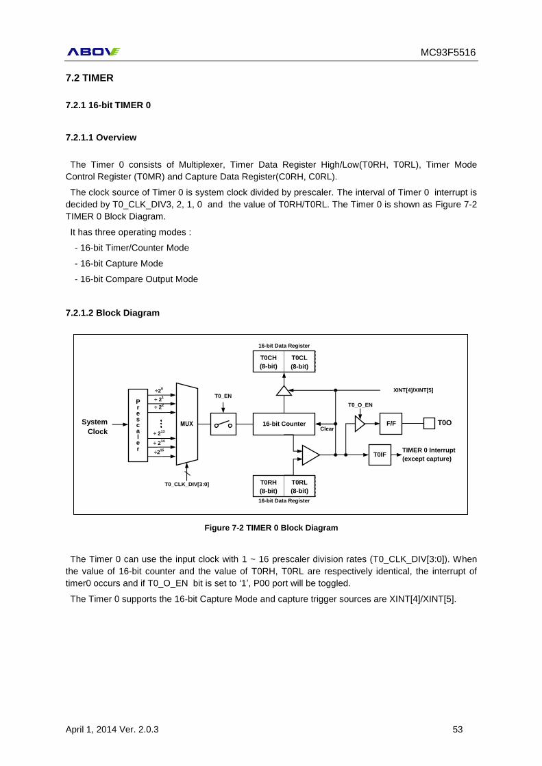
7.2 TIMER
7.2.1 16-bit TIMER 0
7.2.1.1 Overview
The Timer 0 consists of Multiplexer, Timer Data Register High/Low(T0RH, T0RL), Timer Mode
Control Register (T0MR) and Capture Data Register(C0RH, C0RL).
The clock source of Timer 0 is system clock divided by prescaler. The interval of Timer 0 interrupt is
decided by T0_CLK_DIV3, 2, 1, 0 and the value of T0RH/T0RL. The Timer 0 is shown as Figure 7-2
TIMER 0 Block Diagram.
It has three operating modes :
- 16-bit Timer/Counter Mode
- 16-bit Capture Mode
- 16-bit Compare Output Mode
7.2.1.2 Block Diagram
Figure 7-2 TIMER 0 Block Diagram
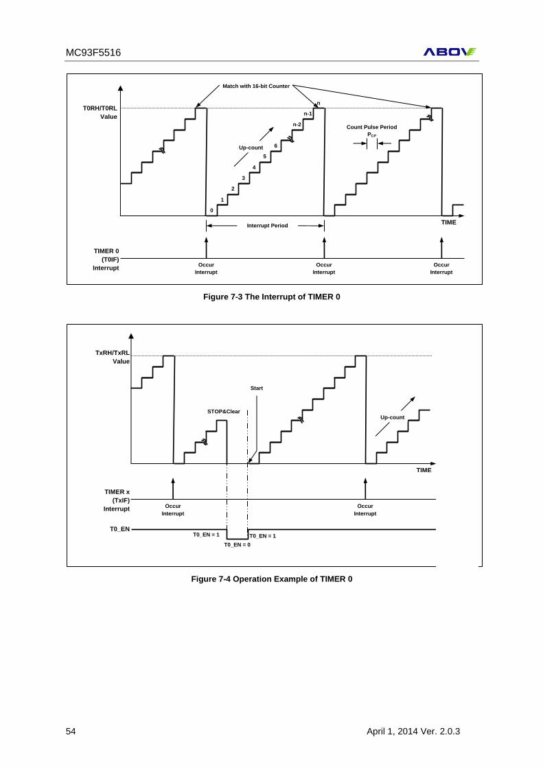
The Timer 0 can use the input clock with 1 ~ 16 prescaler division rates (T0_CLK_DIV[3:0]). When
the value of 16-bit counter and the value of T0RH, T0RL are respectively identical, the interrupt of
timer0 occurs and if T0_O_EN bit is set to ‘1’, P00 port will be toggled.
The Timer 0 supports the 16-bit Capture Mode and capture trigger sources are XINT[4]/XINT[5].
P r e s c a l e r
T0IF
System
Clock
T0_CLK_DIV[3:0]
T0_EN
16-bit Counter
16-bit Data Register
T0RH
(8-bit)
T0RL
(8-bit)
÷20
÷ 21
÷ 22
÷ 213
÷ 214
÷215
TIMER 0 Interrupt
(except capture)
Clear F/F T0O
T0_O_EN
16-bit Data Register
T0CH
(8-bit)
T0CL
(8-bit)
XINT[4]/XINT[5]
MC93F5516
54 April 1, 2014 Ver. 2.0.3
Figure 7-3 The Interrupt of TIMER 0
Figure 7-4 Operation Example of TIMER 0
T0RH/T0RL
Value
TIMER 0
(T0IF)
Interrupt
TIME
1
2
3
4
5
6
n-2
n-1
n
Interrupt Period
0
Count Pulse Period
PCP
Up-count
Match with 16-bit Counter
Occur
Interrupt
Occur
Interrupt
Occur
Interrupt
TIME
STOP&Clear
TIMER x
(TxIF)
Interrupt Occur
Interrupt
Occur
Interrupt
Start
Up-count
T0_EN
T0_EN = 0
T0_EN = 1 T0_EN = 1
TxRH/TxRL
Value

MC93F5516
April 1, 2014 Ver. 2.0.3 55
7.2.1.3 Register Map
Name Address Dir Default Description
T0MR A3H R/W xxH TIMER 0 Mode Control Register
T0RH A4H R/W xxH TIMER 0 High Data Register
T0RL A5H R/W xxH TIMER 0 Low Data Register
T0CL A6H R xxH TIMER 0 Capture Data Register
T0CH A7H R xxH TIMER 0 Capture Data Register
Table 7.2 Timer 0 Register Map
7.2.1.4 TIMER 0 Register description
T0MR (TIMER 0 Mode Control Register) : A3H
7 6 5 4 3 2 1 0
T0_CLK_DIV3 T0_CLK_DIV2 T0_CLK_DIV1 T0_CLK_DIV0 T0_O_EN CAP_EN- CAP_TRG_SEL T0_EN
R/W R/W R/W R/W R/W R/W R/W R/W
Initial value: xxH
T0_CLK_DIV 3,2,1,0
TIMER 0 Clock Divider
DIV3 DIV2 DIV1 DIV0 Description
0 0 0 0 System Clock ÷20
0 0 0 1 System Clock ÷21
0 0 1 0 System Clock ÷22
T0R
Interrupt
Request
(INT0F,INT1F)
XXXXH
Interrupt Interval Period = FFH+01H+FFH+01H+YYH +01H
EXT_INT0,1
PIN
Interrupt
Request
(T0IF,T1IF)
FFFFH FFFFH
YYYYH
00H 00H 00H 00H 00H
Figure 7-5 Express Timer Overflow and Interrupt in Capture Mode
MC93F5516
56 April 1, 2014 Ver. 2.0.3
0 0 1 1 System Clock ÷23
0 1 0 0 System Clock ÷24
0 1 0 1 System Clock ÷25
0 1 1 0 System Clock ÷26
0 1 1 1 System Clock ÷27
1 0 0 0 System Clock ÷28
1 0 0 1 System Clock ÷29
1 0 1 0 System Clock ÷210
1 0 1 1 System Clock ÷211
1 1 0 0 System Clock ÷212
1 1 0 1 System Clock ÷213
1 1 1 0 System Clock ÷214
1 1 1 1 System Clock ÷215
T0_O_EN TIMER 0 Out Enable
0 Disable
1 Enable
CAP_EN Capture Enable
0 Disable
1 Enable
CAP_TRG_SEL Capture Triger Source Selection Bit
0 XINT[4]
1 XINT[5]
T0_EN TIMER 0 Counter Enable bit
0 Disable
1 Enable(When set to ‘1’, 16-bit counter is cleared.
T0RH (TIMER 0 Data MSB Register) : A4H
7 6 5 4 3 2 1 0
T0D15 T0D14 T0D13 T0D12 T0D11 T0D10 T0D9 T0D8
R/W R/W R/W R/W R/W R/W R/W R/W
Initial value: xxH
T0D[15:0] T0 compare high data/P0 compare high data
T0RL (TIMER 0 Data LSB Register) : A5H
7 6 5 4 3 2 1 0
T0D7 T0D6 T0D5 T0D4 T0D3 T0D2 T0D1 T0D0
R/W R/W R/W R/W R/W R/W R/W R/W
Initial value: xxH
T0D[7:0] T0 compare low data/P0 compare low data
MC93F5516
April 1, 2014 Ver. 2.0.3 57
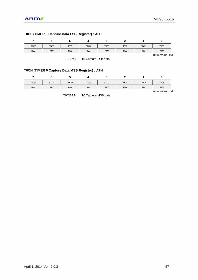
T0CL (TIMER 0 Capture Data LSB Register) : A6H
7 6 5 4 3 2 1 0
T0C7 T0C6 T0C5 T0C4 T0C3 T0C2 T0C1 T0C0
R/W R/W R/W R/W R/W R/W R/W R/W
Initial value: xxH
T0C[7:0] T0 Capture LSB data
T0CH (TIMER 0 Capture Data MSB Register) : A7H
7 6 5 4 3 2 1 0
T0C14 T0C14 T0C13 T0C12 T0C11 T0C10 T0C9 T0C8
R/W R/W R/W R/W R/W R/W R/W R/W
Initial value: xxH
T0C[14:8] T0 Capture MSB data
MC93F5516
58 April 1, 2014 Ver. 2.0.3
7.2.2 8-bit TIMER 1
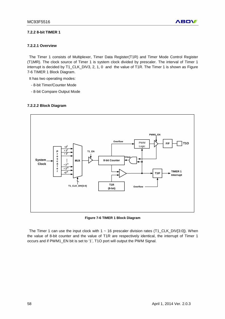
7.2.2.1 Overview
The Timer 1 consists of Multiplexer, Timer Data Register(T1R) and Timer Mode Control Register
(T1MR). The clock source of Timer 1 is system clock divided by prescaler. The interval of Timer 1
interrupt is decided by T1_CLK_DIV3, 2, 1, 0 and the value of T1R. The Timer 1 is shown as Figure
7-6 TIMER 1 Block Diagram.
It has two operating modes:
- 8-bit Timer/Counter Mode
- 8-bit Compare Output Mode
7.2.2.2 Block Diagram
Figure 7-6 TIMER 1 Block Diagram
The Timer 1 can use the input clock with 1 ~ 16 prescaler division rates (T1_CLK_DIV[3:0]). When
the value of 8-bit counter and the value of T1R are respectively identical, the interrupt of Timer 1
occurs and if PWM1_EN bit is set to ‘1’, T1O port will output the PWM Signal.
P r e s c a l e r
T1IF
System
Clock
T1_CLK_DIV[3:0]
T1_EN
8-bit Counter
T1R
(8-bit)
÷20
÷ 21
÷ 22
÷ 213
÷ 214
÷215
TIMER 1
Interrupt
Clear
T1O
PWM1_EN
PWM
Logic
Overflow
F/F
Overflow
MC93F5516
April 1, 2014 Ver. 2.0.3 59
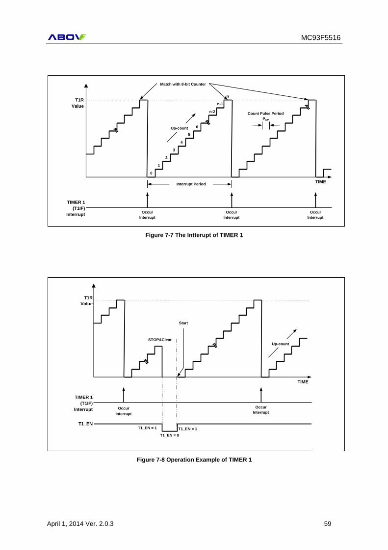
Figure 7-7 The Intterupt of TIMER 1
Figure 7-8 Operation Example of TIMER 1
T1R
Value
TIMER 1
(T1IF)
Interrupt
TIME
1
2
3
4
5
6
n-2
n-1
n
Interrupt Period
0
Count Pulse Period
PCP
Up-count
Match with 8-bit Counter
Occur
Interrupt
Occur
Interrupt
Occur
Interrupt
TIME
STOP&Clear
TIMER 1
(T1IF)
Interrupt Occur
Interrupt
Occur
Interrupt
Start
Up-count
T1_EN
T1_EN = 0
T1_EN = 1 T1_EN = 1
T1R
Value
MC93F5516
60 April 1, 2014 Ver. 2.0.3
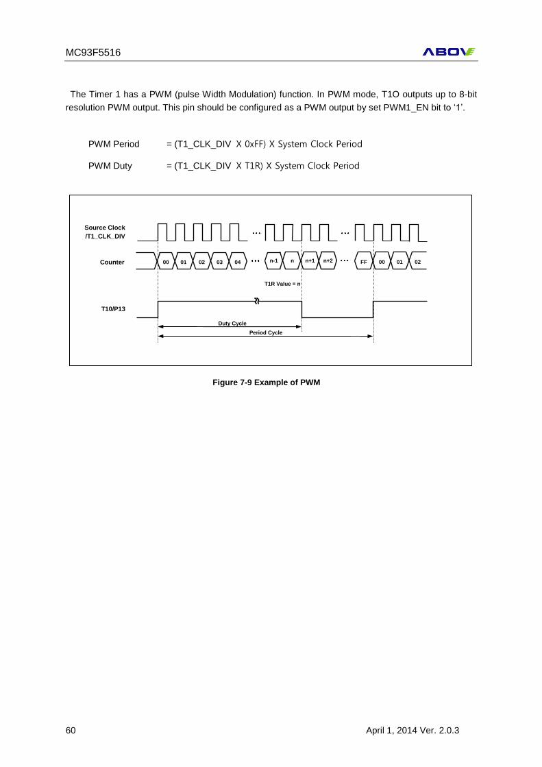
The Timer 1 has a PWM (pulse Width Modulation) function. In PWM mode, T1O outputs up to 8-bit
resolution PWM output. This pin should be configured as a PWM output by set PWM1_EN bit to ‘1’.
PWM Period = (T1_CLK_DIV Х 0xFF) Х System Clock Period
PWM Duty = (T1_CLK_DIV Х T1R) Х System Clock Period
Figure 7-9 Example of PWM
Source Clock
/T1_CLK_DIV
Duty Cycle
T10/P13
Period Cycle
Counter 00
01 02 03 04 n-1 n n+1 n+2 FF 00 01 02
T1R Value = n
MC93F5516
April 1, 2014 Ver. 2.0.3 61
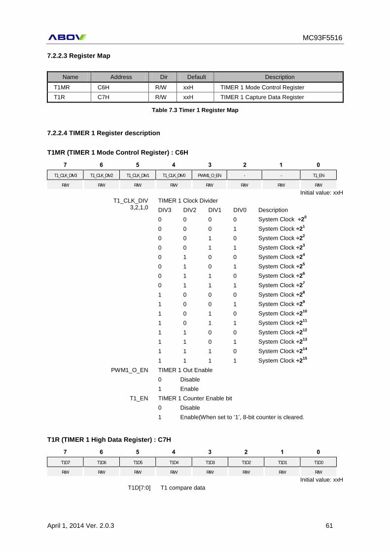
7.2.2.3 Register Map
Name Address Dir Default Description
T1MR C6H R/W xxH TIMER 1 Mode Control Register
T1R C7H R/W xxH TIMER 1 Capture Data Register
Table 7.3 Timer 1 Register Map
7.2.2.4 TIMER 1 Register description
T1MR (TIMER 1 Mode Control Register) : C6H
7 6 5 4 3 2 1 0
T1_CLK_DIV3 T1_CLK_DIV2 T1_CLK_DIV1 T1_CLK_DIV0 PWM1_O_EN - - T1_EN
R/W R/W R/W R/W R/W R/W R/W R/W
Initial value: xxH
T1_CLK_DIV 3,2,1,0
TIMER 1 Clock Divider
DIV3 DIV2 DIV1 DIV0 Description
0 0 0 0 System Clock ÷20
0 0 0 1 System Clock ÷21
0 0 1 0 System Clock ÷22
0 0 1 1 System Clock ÷23
0 1 0 0 System Clock ÷24
0 1 0 1 System Clock ÷25
0 1 1 0 System Clock ÷26
0 1 1 1 System Clock ÷27
1 0 0 0 System Clock ÷28
1 0 0 1 System Clock ÷29
1 0 1 0 System Clock ÷210
1 0 1 1 System Clock ÷211
1 1 0 0 System Clock ÷212
1 1 0 1 System Clock ÷213
1 1 1 0 System Clock ÷214
1 1 1 1 System Clock ÷215
PWM1_O_EN TIMER 1 Out Enable
0 Disable
1 Enable
T1_EN TIMER 1 Counter Enable bit
0 Disable
1 Enable(When set to ‘1’, 8-bit counter is cleared.
T1R (TIMER 1 High Data Register) : C7H
7 6 5 4 3 2 1 0
T1D7 T1D6 T1D5 T1D4 T1D3 T1D2 T1D1 T1D0
R/W R/W R/W R/W R/W R/W R/W R/W
Initial value: xxH
T1D[7:0] T1 compare data

MC93F5516
62 April 1, 2014 Ver. 2.0.3
7.3 I2C
7.3.1 Overview
The I2C is one of industrial standard serial communication protocols, and which uses 2 bus lines
Serial Data Line (SDA) and Serial Clock Line (SCL) to exchange data. Because both SDA and SCL
lines are open-drain output, each line needs pull-up resistor. The features are as shown below.
- Compatible with I2C bus standard
- Multi-master operation
- Up to 400 KHz data transfer speed
- 7 bit address
- Both master and slave operation
- Bus busy detection
7.3.2 Block Diagram
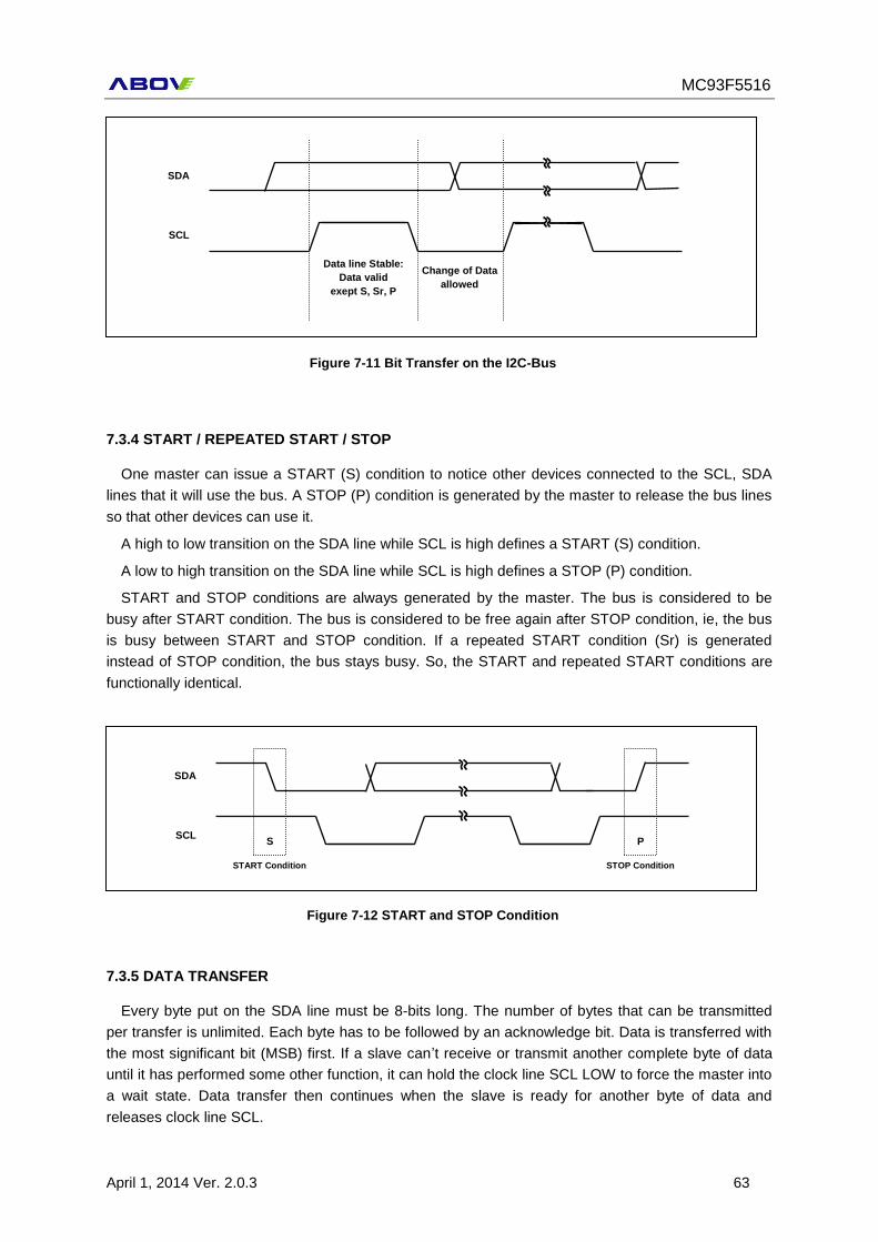
7.3.3 I2C Bit Transfer
The data on the SDA line must be stable during HIGH period of the clock, SCL. The HIGH or LOW
state of the data line can only change when the clock signal on the SCL line is LOW. The exceptions
are START(S), repeated START(Sr) and STOP(P) condition where data line changes when clock line
is high.
SDA F/F 8-bit Shift Register
(SHFTR)
Slave Address Register
(SVADR)
Noise
Canceller
(debounce)
Data Out Register
(I2CDR)
(I2CSCLHR)
(I2CSCLLR)
(I2CDAHR)
SDA
Out Controller
SCL
Out Controller SCL
Noise
Canceller
(debounce)
I
n
t
e
r
n
a
l
B
u
s
L
i
n
SDAIN
SDAOUT
SCLIN
SCLOUT
1
0
1
0
Debounce
enable
Debounce
enable
Figure 7-10 I2C Block Diagram
MC93F5516
April 1, 2014 Ver. 2.0.3 63
7.3.4 START / REPEATED START / STOP
One master can issue a START (S) condition to notice other devices connected to the SCL, SDA
lines that it will use the bus. A STOP (P) condition is generated by the master to release the bus lines
so that other devices can use it.
A high to low transition on the SDA line while SCL is high defines a START (S) condition.
A low to high transition on the SDA line while SCL is high defines a STOP (P) condition.
START and STOP conditions are always generated by the master. The bus is considered to be
busy after START condition. The bus is considered to be free again after STOP condition, ie, the bus
is busy between START and STOP condition. If a repeated START condition (Sr) is generated
instead of STOP condition, the bus stays busy. So, the START and repeated START conditions are
functionally identical.
7.3.5 DATA TRANSFER
Every byte put on the SDA line must be 8-bits long. The number of bytes that can be transmitted
per transfer is unlimited. Each byte has to be followed by an acknowledge bit. Data is transferred with
the most significant bit (MSB) first. If a slave can’t receive or transmit another complete byte of data
until it has performed some other function, it can hold the clock line SCL LOW to force the master into
a wait state. Data transfer then continues when the slave is ready for another byte of data and
releases clock line SCL.
SCL
SDA
Data line Stable:
Data valid
exept S, Sr, P
Change of Data
allowed
Figure 7-11 Bit Transfer on the I2C-Bus
SCL
SDA
START Condition
S P
STOP Condition
Figure 7-12 START and STOP Condition
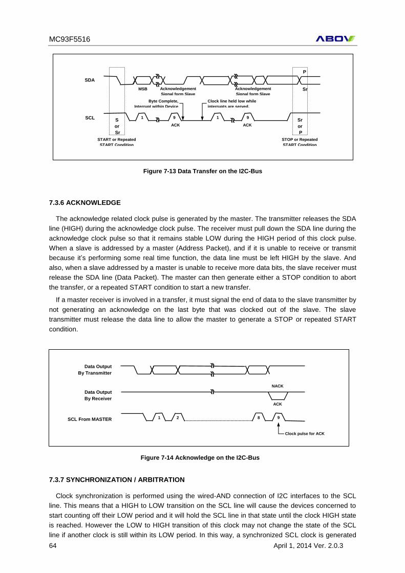
MC93F5516
64 April 1, 2014 Ver. 2.0.3
7.3.6 ACKNOWLEDGE
The acknowledge related clock pulse is generated by the master. The transmitter releases the SDA
line (HIGH) during the acknowledge clock pulse. The receiver must pull down the SDA line during the
acknowledge clock pulse so that it remains stable LOW during the HIGH period of this clock pulse.
When a slave is addressed by a master (Address Packet), and if it is unable to receive or transmit
because it’s performing some real time function, the data line must be left HIGH by the slave. And
also, when a slave addressed by a master is unable to receive more data bits, the slave receiver must
release the SDA line (Data Packet). The master can then generate either a STOP condition to abort
the transfer, or a repeated START condition to start a new transfer.
If a master receiver is involved in a transfer, it must signal the end of data to the slave transmitter by
not generating an acknowledge on the last byte that was clocked out of the slave. The slave
transmitter must release the data line to allow the master to generate a STOP or repeated START
condition.
7.3.7 SYNCHRONIZATION / ARBITRATION
Clock synchronization is performed using the wired-AND connection of I2C interfaces to the SCL
line. This means that a HIGH to LOW transition on the SCL line will cause the devices concerned to
start counting off their LOW period and it will hold the SCL line in that state until the clock HIGH state
is reached. However the LOW to HIGH transition of this clock may not change the state of the SCL
line if another clock is still within its LOW period. In this way, a synchronized SCL clock is generated
1 2 8
Data Output
By Transmitter
9
ACK
NACK
Clock pulse for ACK
Data Output
By Receiver
SCL From MASTER
START or Repeated
START Condition
S
or
Sr
STOP or Repeated
START Condition
Sr
or
P
MSB Acknowledgement
Signal form Slave
Acknowledgement
Signal form Slave
Byte Complete,
Interrupt within Device
Clock line held low while
interrupts are served.
1 9 1 9
ACK ACK
SDA
SCL
Sr
P
Figure 7-13 Data Transfer on the I2C-Bus
Figure 7-14 Acknowledge on the I2C-Bus
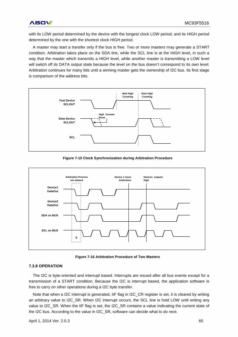
MC93F5516
April 1, 2014 Ver. 2.0.3 65
with its LOW period determined by the device with the longest clock LOW period, and its HIGH period
determined by the one with the shortest clock HIGH period.
A master may start a transfer only if the bus is free. Two or more masters may generate a START
condition. Arbitration takes place on the SDA line, while the SCL line is at the HIGH level, in such a
way that the master which transmits a HIGH level, while another master is transmitting a LOW level
will switch off its DATA output state because the level on the bus doesn’t correspond to its own level.
Arbitration continues for many bits until a winning master gets the ownership of I2C bus. Its first stage
is comparison of the address bits.
7.3.8 OPERATION
The I2C is byte-oriented and interrupt based. Interrupts are issued after all bus events except for a
transmission of a START condition. Because the I2C is interrupt based, the application software is
free to carry on other operations during a I2C byte transfer.
Note that when a I2C interrupt is generated, IIF flag in I2C_CR register is set, it is cleared by writing
an arbitrary value to I2C_SR. When I2C interrupt occurs, the SCL line is hold LOW until writing any
value to I2C_SR. When the IIF flag is set, the I2C_SR contains a value indicating the current state of
the I2C bus. According to the value in I2C_SR, software can decide what to do next.
High Counter
Reset
Fast Device
SCLOUT
Slow Device
SCLOUT
SCL
Wait High
Counting
Start High
Counting
Device1
DataOut
SCL on BUS
Device2
DataOut
SDA on BUS
S
Arbitration Process
not adaped
Device 1 loses
Arbitration
Device1 outputs
High
Figure 7-15 Clock Synchronization during Arbitration Procedure
Figure 7-16 Arbitration Procedure of Two Masters
MC93F5516
66 April 1, 2014 Ver. 2.0.3
I2C can operate in 4 modes by configuring master/slave, transmitter/receiver. The operating mode
is configured by a winning master. A more detailed explanation follows below.
7.3.8.1 Master Transmitter
To operate I2C in master transmitter, follow the recommended steps below.
1. Enable I2C by setting IICEN bit in I2C_CR. This provides main clock to the peripheral.
2. Load SLA+W into the I2C_DR where SLA is address of slave device and W is transfer direction from the viewpoint of the master. For master transmitter, W is ‘0’. Note that I2C_DR is used for both address and data.
3. Configure baud rate by writing desired value to both I2C_SCLLR and I2C_SCLHR for the Low and High period of SCL line.
4. Configure the I2C_SDHR to decide when SDA changes value from falling edge of SCL. If SDA should change in the middle of SCL LOW period, load half the value of I2C_SCLLR to the I2C_SDHR.
5. Set the START bit in I2C_CR. This transmits a START condition. And also configure how to handle interrupt and ACK signal. When the START bit is set, 8-bit data in I2C_DR is transmitted out according to the baud-rate.
6. This is ACK signal processing stage for address packet transmitted by master. When 7-bit address and 1-bit transfer direction is transmitted to target slave device, the master can know whether the slave acknowledged or not in the 9
th high period of SCL. If the master gains bus
mastership, I2C generates GCALL interrupt regardless of the reception of ACK from the slave device. When I2C loses bus mastership during arbitration process, the MLOST bit in I2C_SR is set, and I2C waits in idle state or can be operate as an addressed slave. To operate as a slave when the MLSOT bit in I2C_SR is set, the ACKEN bit in I2C_CR must be set and the received 7-bit address must equal to the SLA bits in I2C_SAR. In this case I2C operates as a slave transmitter or a slave receiver (go to appropriate section). In this stage, I2C holds the SCL LOW. This is because to decide whether I2C continues serial transfer or stops communication. The following steps continue assuming that I2C does not lose mastership during first data transfer. I2C (Master) can choose one of the following cases regardless of the reception of ACK signal from slave. 1) Master receives ACK signal from slave, so continues data transfer because slave can receive more data from master. In this case, load data to transmit to I2C_DR. 2) Master stops data transfer even if it receives ACK signal from slave. In this case, set the STOP bit in I2C_CR. 3) Master transmits repeated START condition with not checking ACK signal. In this case, load SLA+R/W into the I2C_DR and set START bit in I2C_CR. After doing one of the actions above, write arbitrary value to I2C_SR to release SCL line. In case of 1), move to step 7. In case of 2), move to step 9 to handle STOP interrupt. In case of 3), move to step 6 after transmitting the data in I2C_DR and if transfer direction bit is ‘1’ go to master receiver section.
7. 1-Byte of data is being transmitted. During data transfer, bus arbitration continues.
8. This is ACK signal processing stage for data packet transmitted by master. I2C holds the SCL LOW. When I2C loses bus mastership while transmitting data arbitrating other masters, the MLOST bit in I2C_SR is set. If then, I2C waits in idle state. When the data in I2C_DR is transmitted completely, I2C generates TEND interrupt. I2C can choose one of the following cases regardless of the reception of ACK signal from slave. 1) Master receives ACK signal from slave, so continues data transfer because slave can receive more data from master. In this case, load data to transmit to I2C_DR. 2) Master stops data transfer even if it receives ACK signal from slave. In this case, set the STOP bit in I2C_CR.
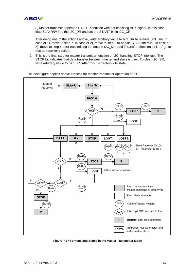
MC93F5516
April 1, 2014 Ver. 2.0.3 67
3) Master transmits repeated START condition with not checking ACK signal. In this case, load SLA+R/W into the I2C_DR and set the START bit in I2C_CR. After doing one of the actions above, write arbitrary value to I2C_SR to release SCL line. In case of 1), move to step 7. In case of 2), move to step 9 to handle STOP interrupt. In case of 3), move to step 6 after transmitting the data in I2C_DR, and if transfer direction bit is ‘1’ go to master receiver section.
9. This is the final step for master transmitter function of I2C, handling STOP interrupt. The STOP bit indicates that data transfer between master and slave is over. To clear I2C_SR, write arbitrary value to I2C_SR. After this, I2C enters idle state.
The next figure depicts above process for master transmitter operation of I2C.
From master to slave /
Master command or Data Write
From slave to master
0xxx Value of Status Register
ACK Interrupt, SCL line is held low
Interrupt after stop command P
Arbitration lost as master and
addressed as slave LOST&
Other master continues
Slave Receiver (0x1D)
or Transmitter (0x1F)
Master
Receiver
SLA+W
ACK
DATA
Rs
STOP
LOST
LOST&
STOP
LOST
S or Sr
SLA+R
Y
N
0x0E 0x87
0x86
0x0E
ACK STOP
Y
N
0x0F 0x1D
Lost? Y
0x47
0x1F
0x46
Cont? Y
N
STOP
0x0F
LOST
P
0x22
P
0x22
0x22
P
Figure 7-17 Formats and States in the Master Transmitter Mode

MC93F5516
68 April 1, 2014 Ver. 2.0.3
7.3.8.2 Master Receiver
To operate I2C in master receiver, follow the recommended steps below.
1. Enable I2C by setting IICEN bit in I2C_CR. This provides main clock to the peripheral.
2. Load SLA+R into the I2C_DR where SLA is address of slave device and R is transfer direction from the viewpoint of the master. For master receiver, R is ‘1’. Note that I2C_DR is used for both address and data.
3. Configure baud rate by writing desired value to both I2C_SCLLR and I2C_SCLHR for the Low and High period of SCL line.
4. Configure the I2C_SDHR to decide when SDA changes value from falling edge of SCL. If SDA should change in the middle of SCL LOW period, load half the value of I2C_SCLLR to the I2C_SDHR.
5. Set the START bit in I2C_CR. This transmits a START condition. And also configure how to handle interrupt and ACK signal. When the START bit is set, 8-bit data in I2C_DR is transmitted out according to the baud-rate.
6. This is ACK signal processing stage for address packet transmitted by master. When 7-bit address and 1-bit transfer direction is transmitted to target slave device, the master can know whether the slave acknowledged or not in the 9
th high period of SCL. If the master gains bus
mastership, I2C generates GCALL interrupt regardless of the reception of ACK from the slave device. When I2C loses bus mastership during arbitration process, the MLOST bit in I2C_SR is set, and I2C waits in idle state or can be operate as an addressed slave. To operate as a slave when the MLSOT bit in I2C_SR is set, the ACKEN bit in I2C_CR must be set and the received 7-bit address must equal to the SLA bits in I2C_SAR. In this case I2C operates as a slave transmitter or a slave receiver (go to appropriate section). In this stage, I2C holds the SCL LOW. This is because to decide whether I2C continues serial transfer or stops communication. The following steps continue assuming that I2C does not lose mastership during first data transfer. I2C (Master) can choose one of the following cases according to the reception of ACK signal from slave. 1) Master receives ACK signal from slave, so continues data transfer because slave can prepare and transmit more data to master. Configure ACKEN bit in I2C_CR to decide whether I2C ACKnowledges the next data to be received or not. 2) Master stops data transfer because it receives no ACK signal from slave. In this case, set the STOP bit in I2C_CR. 3) Master transmits repeated START condition due to no ACK signal from slave. In this case, load SLA+R/W into the I2C_DR and set START bit in I2C_CR. After doing one of the actions above, write arbitrary value to I2C_SR to release SCL line. In case of 1), move to step 7. In case of 2), move to step 9 to handle STOP interrupt. In case of 3), move to step 6 after transmitting the data in I2C_DR and if transfer direction bit is ‘0’ go to master transmitter section.
7. 1-Byte of data is being received.
8. This is ACK signal processing stage for data packet transmitted by slave. I2C holds the SCL LOW. When 1-Byte of data is received completely, I2C generates TEND interrupt. I2C can choose one of the following cases according to the RXACK flag in I2C_SR. 1) Master continues receiving data from slave. To do this, set ACKEN bit in I2C_CR to ACKnowledge the next data to be received. 2) Master wants to terminate data transfer when it receives next data by not generating ACK signal. This can be done by clearing ACKEN bit in I2C_CR. 3) Because no ACK signal is detected, master terminates data transfer. In this case, set the STOP bit in I2C_CR. 4) No ACK signal is detected, and master transmits repeated START condition. In this case, load SLA+R/W into the I2C_DR and set the START bit in I2C_CR.
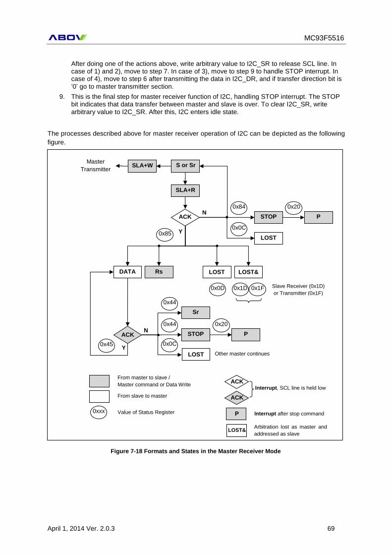
MC93F5516
April 1, 2014 Ver. 2.0.3 69
After doing one of the actions above, write arbitrary value to I2C_SR to release SCL line. In case of 1) and 2), move to step 7. In case of 3), move to step 9 to handle STOP interrupt. In case of 4), move to step 6 after transmitting the data in I2C_DR, and if transfer direction bit is ‘0’ go to master transmitter section.
9. This is the final step for master receiver function of I2C, handling STOP interrupt. The STOP bit indicates that data transfer between master and slave is over. To clear I2C_SR, write arbitrary value to I2C_SR. After this, I2C enters idle state.
The processes described above for master receiver operation of I2C can be depicted as the following
figure.
From master to slave /
Master command or Data Write
From slave to master
0xxx Value of Status Register
ACK Interrupt, SCL line is held low
Interrupt after stop command P
ACK
Arbitration lost as master and
addressed as slave LOST&
Other master continues
Slave Receiver (0x1D)
or Transmitter (0x1F)
Master
Transmitter
SLA+R
ACK
DATA
Rs
LOST
LOST&
STOP
LOST
S or Sr
SLA+W
Y
N
0x0C 0x85
0x84
0x0C
ACK STOP
Y
N
0x0D 0x1D
0x45
0x1F
0x44
LOST
P
0x20
P
0x20
Sr
0x44
Figure 7-18 Formats and States in the Master Receiver Mode
MC93F5516
70 April 1, 2014 Ver. 2.0.3
7.3.8.3 Slave Transmitter
To operate I2C in slave transmitter, follow the recommended steps below.
1. If the main operating clock (SCLK) of the system is slower than that of SCL, load value 0x00 into I2C_SDHR to make SDA change within one system clock period from the falling edge of SCL. Note that the hold time of SDA is calculated by SDAH x period of SCLK where SDAH is multiple of number of SCLK coming from I2C_SDHR. When the hold time of SDA is longer than the period of SCLK, I2C (slave) cannot transmit serial data properly.
2. Enable I2C by setting IICEN bit and INTEN bit in I2C_CR. This provides main clock to the peripheral.
3. When a START condition is detected, I2C receives one byte of data and compares it with SLA bits in I2C_SAR. If the GCALLEN bit in I2C_SAR is enabled, I2C compares the received data with value 0x00, the general call address.
4. If the received address does not equal to SLA bits in I2C_SAR, I2C enters idle state ie, waits for another START condition. Else if the address equals to SLA bits and the ACKEN bit is enabled, I2C generates SSEL interrupt and the SCL line is held LOW. Note that even if the address equals to SLA bits, when the ACKEN bit is disabled, I2C enters idle state. When SSEL interrupt occurs, load transmit data to I2C_DR and write arbitrary value to I2C_SR to release SCL line.
5. 1-Byte of data is being transmitted.
6. In this step, I2C generates TEND interrupt and holds the SCL line LOW regardless of the reception of ACK signal from master. Slave can select one of the following cases. 1) No ACK signal is detected and I2C waits STOP or repeated START condition. 2) ACK signal from master is detected. Load data to transmit into I2C_DR. After doing one of the actions above, write arbitrary value to I2C_SR to release SCL line. In case of 1) move to step 7 to terminate communication. In case of 2) move to step 5. In either case, a repeated START condition can be detected. For that case, move step 4.
7. This is the final step for slave transmitter function of I2C, handling STOP interrupt. The STOP bit indicates that data transfer between master and slave is over. To clear I2C_SR, write arbitrary value to I2C_SR. After this, I2C enters idle state.
The next figure shows flow chart for handling slave transmitter function of I2C.
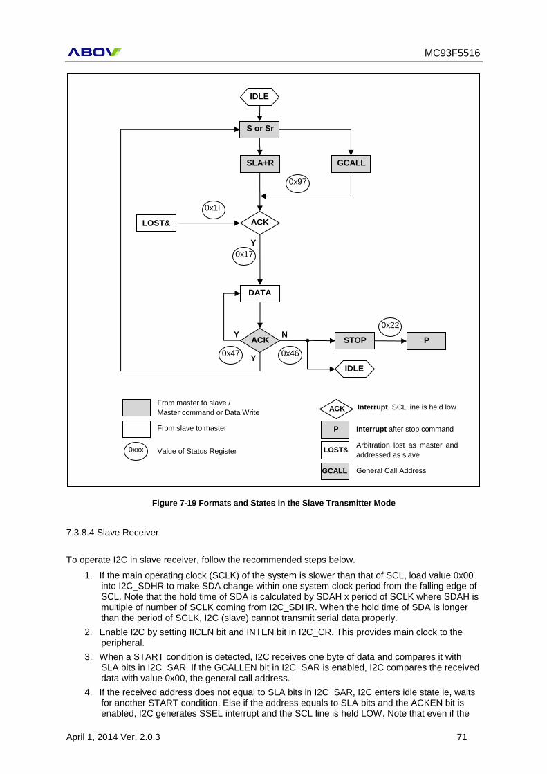
MC93F5516
April 1, 2014 Ver. 2.0.3 71
7.3.8.4 Slave Receiver
To operate I2C in slave receiver, follow the recommended steps below.
1. If the main operating clock (SCLK) of the system is slower than that of SCL, load value 0x00 into I2C_SDHR to make SDA change within one system clock period from the falling edge of SCL. Note that the hold time of SDA is calculated by SDAH x period of SCLK where SDAH is multiple of number of SCLK coming from I2C_SDHR. When the hold time of SDA is longer than the period of SCLK, I2C (slave) cannot transmit serial data properly.
2. Enable I2C by setting IICEN bit and INTEN bit in I2C_CR. This provides main clock to the peripheral.
3. When a START condition is detected, I2C receives one byte of data and compares it with SLA bits in I2C_SAR. If the GCALLEN bit in I2C_SAR is enabled, I2C compares the received data with value 0x00, the general call address.
4. If the received address does not equal to SLA bits in I2C_SAR, I2C enters idle state ie, waits for another START condition. Else if the address equals to SLA bits and the ACKEN bit is enabled, I2C generates SSEL interrupt and the SCL line is held LOW. Note that even if the
SLA+R
ACK
DATA
LOST&
S or Sr
Y
0x47
ACK STOP
Y
N
0x46
P
0x22
IDLE
IDLE
Y
GCALL
0x1F
0x97
0x17
From master to slave /
Master command or Data Write
From slave to master
0xxx Value of Status Register
ACK Interrupt, SCL line is held low
Interrupt after stop command P
Arbitration lost as master and
addressed as slave LOST&
General Call Address GCALL
Figure 7-19 Formats and States in the Slave Transmitter Mode
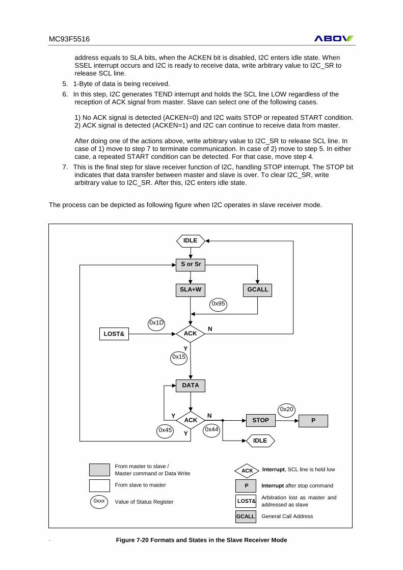
MC93F5516
72 April 1, 2014 Ver. 2.0.3
address equals to SLA bits, when the ACKEN bit is disabled, I2C enters idle state. When SSEL interrupt occurs and I2C is ready to receive data, write arbitrary value to I2C_SR to release SCL line.
5. 1-Byte of data is being received.
6. In this step, I2C generates TEND interrupt and holds the SCL line LOW regardless of the reception of ACK signal from master. Slave can select one of the following cases. 1) No ACK signal is detected (ACKEN=0) and I2C waits STOP or repeated START condition. 2) ACK signal is detected (ACKEN=1) and I2C can continue to receive data from master. After doing one of the actions above, write arbitrary value to I2C_SR to release SCL line. In case of 1) move to step 7 to terminate communication. In case of 2) move to step 5. In either case, a repeated START condition can be detected. For that case, move step 4.
7. This is the final step for slave receiver function of I2C, handling STOP interrupt. The STOP bit indicates that data transfer between master and slave is over. To clear I2C_SR, write arbitrary value to I2C_SR. After this, I2C enters idle state.
The process can be depicted as following figure when I2C operates in slave receiver mode.
SLA+W
ACK
DATA
LOST&
S or Sr
Y
N
0x45
ACK STOP
Y
N
0x44
P
0x20
IDLE
IDLE
Y
GCALL
0x1D
0x95
0x15
From master to slave /
Master command or Data Write
From slave to master
0xxx Value of Status Register
ACK Interrupt, SCL line is held low
Interrupt after stop command P
Arbitration lost as master and
addressed as slave LOST&
General Call Address GCALL
Figure 7-20 Formats and States in the Slave Receiver Mode
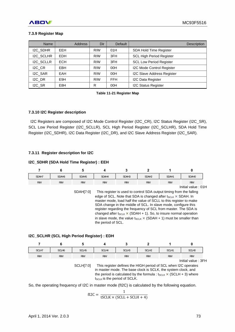
MC93F5516
April 1, 2014 Ver. 2.0.3 73
7.3.9 Register Map
Name Address Dir Default Description
I2C_SDHR EEH R/W 01H SDA Hold Time Register
I2C_SCLHR EDH R/W 3FH SCL High Period Register
I2C_SCLLR ECH R/W 3FH SCL Low Period Register
I2C_CR EBH R/W 00H I2C Mode Control Register
I2C_SAR EAH R/W 00H I2C Slave Address Register
I2C_DR E9H R/W FFH I2C Data Register
I2C_SR E8H R 00H I2C Status Register
Table 11-21 Register Map
7.3.10 I2C Register description
I2C Registers are composed of I2C Mode Control Register (I2C_CR), I2C Status Register (I2C_SR),
SCL Low Period Register (I2C_SCLLR), SCL High Period Register (I2C_SCLHR), SDA Hold Time
Register (I2C_SDHR), I2C Data Register (I2C_DR), and I2C Slave Address Register (I2C_SAR).
7.3.11 Register description for I2C
I2C_SDHR (SDA Hold Time Register) : EEH
7 6 5 4 3 2 1 0
SDAH7 SDAH6 SDAH5 SDAH4 SDAH3 SDAH2 SDAH1 SDAH0
R/W R/W R/W R/W R/W R/W R/W R/W
Initial value : 01H
SDAH[7:0] This register is used to control SDA output timing from the falling
edge of SCL. Note that SDA is changed after tSCLK SDAH. In
master mode, load half the value of SCLL to this register to make SDA change in the middle of SCL. In slave mode, configure this register regarding the frequency of SCL from master. The SDA is
changed after tSCLK (SDAH + 1). So, to insure normal operation
in slave mode, the value tSCLK (SDAH + 1) must be smaller than
the period of SCL.
I2C_SCLHR (SCL High Period Register) : EDH
7 6 5 4 3 2 1 0
SCLH7 SCLH6 SCLH5 SCLH4 SCLH3 SCLH2 SCLH1 SCLH0
R/W R/W R/W R/W R/W R/W R/W R/W
Initial value : 3FH
SCLH[7:0] This register defines the HIGH period of SCL when I2C operates in master mode. The base clock is SCLK, the system clock, and
the period is calculated by the formula : tSCLK (SCLH + 3) where
tSCLK is the period of SCLK.
So, the operating frequency of I2C in master mode (fI2C) is calculated by the following equation.
2
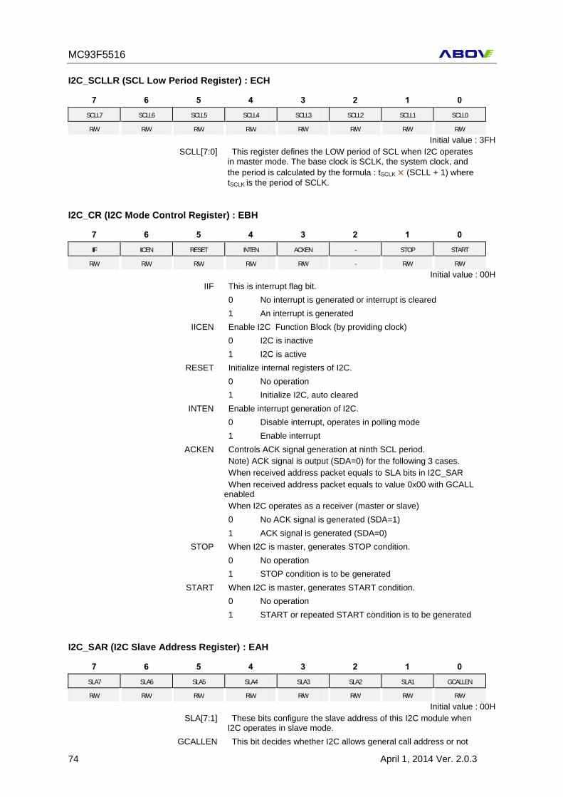
MC93F5516
74 April 1, 2014 Ver. 2.0.3
I2C_SCLLR (SCL Low Period Register) : ECH
7 6 5 4 3 2 1 0
SCLL7 SCLL6 SCLL5 SCLL4 SCLL3 SCLL2 SCLL1 SCLL0
R/W R/W R/W R/W R/W R/W R/W R/W
Initial value : 3FH
SCLL[7:0] This register defines the LOW period of SCL when I2C operates in master mode. The base clock is SCLK, the system clock, and
the period is calculated by the formula : tSCLK (SCLL + 1) where
tSCLK is the period of SCLK.
I2C_CR (I2C Mode Control Register) : EBH
7 6 5 4 3 2 1 0
IIF IICEN RESET INTEN ACKEN - STOP START
R/W R/W R/W R/W R/W - R/W R/W
Initial value : 00H
IIF This is interrupt flag bit.
0 No interrupt is generated or interrupt is cleared
1 An interrupt is generated
IICEN Enable I2C Function Block (by providing clock)
0 I2C is inactive
1 I2C is active
RESET Initialize internal registers of I2C.
0 No operation
1 Initialize I2C, auto cleared
INTEN Enable interrupt generation of I2C.
0 Disable interrupt, operates in polling mode
1 Enable interrupt
ACKEN Controls ACK signal generation at ninth SCL period.
Note) ACK signal is output (SDA=0) for the following 3 cases.
When received address packet equals to SLA bits in I2C_SAR
When received address packet equals to value 0x00 with GCALL enabled
When I2C operates as a receiver (master or slave)
0 No ACK signal is generated (SDA=1)
1 ACK signal is generated (SDA=0)
STOP When I2C is master, generates STOP condition.
0 No operation
1 STOP condition is to be generated
START When I2C is master, generates START condition.
0 No operation
1 START or repeated START condition is to be generated
I2C_SAR (I2C Slave Address Register) : EAH
7 6 5 4 3 2 1 0
SLA7 SLA6 SLA5 SLA4 SLA3 SLA2 SLA1 GCALLEN
R/W R/W R/W R/W R/W R/W R/W R/W
Initial value : 00H
SLA[7:1] These bits configure the slave address of this I2C module when I2C operates in slave mode.
GCALLEN This bit decides whether I2C allows general call address or not
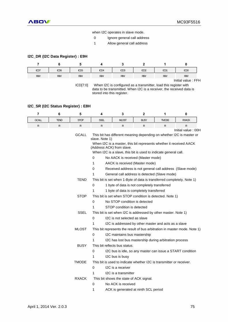
MC93F5516
April 1, 2014 Ver. 2.0.3 75
when I2C operates in slave mode.
0 Ignore general call address
1 Allow general call address
I2C_DR (I2C Data Register) : E9H
7 6 5 4 3 2 1 0
ICD7 ICD6 ICD5 ICD4 ICD3 ICD2 ICD1 ICD0
R/W R/W R/W R/W R/W R/W R/W R/W
Initial value : FFH
ICD[7:0] When I2C is configured as a transmitter, load this register with data to be transmitted. When I2C is a receiver, the received data is stored into this register.
I2C_SR (I2C Status Register) : E8H
7 6 5 4 3 2 1 0
GCALL TEND STOP SSEL MLOST BUSY TMODE RXACK
R R R R R R R R
Initial value : 00H
GCALL This bit has different meaning depending on whether I2C is master or slave. Note 1)
When I2C is a master, this bit represents whether it received AACK (Address ACK) from slave.
When I2C is a slave, this bit is used to indicate general call.
0 No AACK is received (Master mode)
1 AACK is received (Master mode)
0 Received address is not general call address (Slave mode)
1 General call address is detected (Slave mode)
TEND This bit is set when 1-Byte of data is transferred completely. Note 1)
0 1 byte of data is not completely transferred
1 1 byte of data is completely transferred
STOP This bit is set when STOP condition is detected. Note 1)
0 No STOP condition is detected
1 STOP condition is detected
SSEL This bit is set when I2C is addressed by other master. Note 1)
0 I2C is not selected as slave
1 I2C is addressed by other master and acts as a slave
MLOST This bit represents the result of bus arbitration in master mode. Note 1)
0 I2C maintains bus mastership
1 I2C has lost bus mastership during arbitration process
BUSY This bit reflects bus status.
0 I2C bus is idle, so any master can issue a START condition
1 I2C bus is busy
TMODE This bit is used to indicate whether I2C is transmitter or receiver.
0 I2C is a receiver
1 I2C is a transmitter
RXACK This bit shows the state of ACK signal.
0 No ACK is received
1 ACK is generated at ninth SCL period
MC93F5516
76 April 1, 2014 Ver. 2.0.3
Note 1) These bits can be source of interrupt.
When an I2C interrupt occurs except for STOP interrupt, the SCL line is hold LOW. To release SCL, write arbitrary value to I2C_SR. When I2C_SR is written, the TEND, STOP, SSEL, LOST, RXACK bits are cleared.
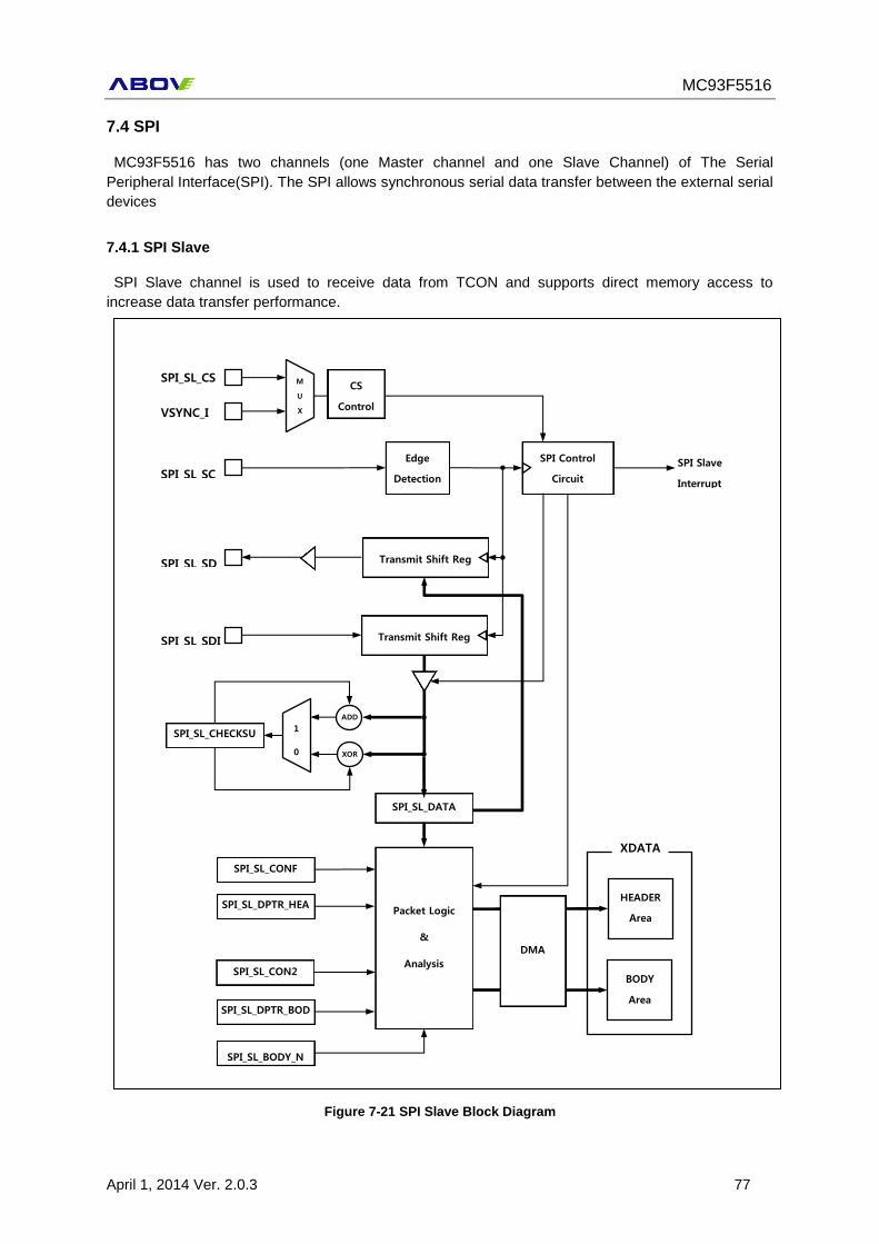
MC93F5516
April 1, 2014 Ver. 2.0.3 77
7.4 SPI
MC93F5516 has two channels (one Master channel and one Slave Channel) of The Serial
Peripheral Interface(SPI). The SPI allows synchronous serial data transfer between the external serial
devices
7.4.1 SPI Slave
SPI Slave channel is used to receive data from TCON and supports direct memory access to
increase data transfer performance.
Figure 7-21 SPI Slave Block Diagram
Edge
Detection
SPI Control
Circuit SPI_SL_SC
SPI_SL_SD
SPI_SL_SDI
SPI Slave
Interrupt
SPI_SL_CS
B VSYNC_I
N
SPI_SL_CHECKSU
M
ADD
XOR
1
0
SPI_SL_DATA
Packet Logic
&
Analysis SPI_SL_CON2
HEADER
Area
BODY
Area
M
U
X
CS
Control
SPI_SL_CONF
XDATA
Transmit Shift Reg
SPI_SL_DPTR_HEA
D
SPI_SL_DPTR_BOD
Y
SPI_SL_BODY_N
DMA
Transmit Shift Reg
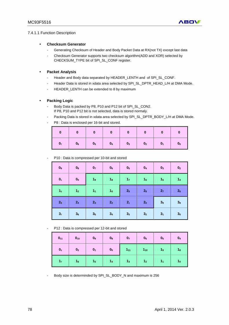
MC93F5516
78 April 1, 2014 Ver. 2.0.3
7.4.1.1 Function Description
Checksum Generator
- Generating Checksum of Header and Body Packet Data at RX(not TX) except last data
- Checksum Generator supports two checksum algorithm(ADD and XOR) selected by
CHECKSUM_TYPE bit of SPI_SL_CONF register.
Packet Analysis
- Header and Body data separated by HEADER_LENTH and of SPI_SL_CONF.
- Header Data is stored in xdata area selected by SPI_SL_DPTR_HEAD_L/H at DMA Mode.
- HEADER_LENTH can be extended to 8 by maximum
Packing Logic
- Body Data is packed by P8, P10 and P12 bit of SPI_SL_CON2.
If P8, P10 and P12 bit is not selected, data is stored normaly.
- Packing Data is stored in xdata area selected by SPI_SL_DPTR_BODY_L/H at DMA Mode.
- P8 : Data is enclosed per 16-bit and stored.
0 0 0 0 0 0 0 0
07 06 05 04 03 02 01 00
- P10 : Data is compressed per 10-bit and stored
09 08 07 06 05 04 03 02
01 00 19 18 17 16 15 14
13 12 11 10 29 28 27 26
25 24 23 22 21 20 39 38
37 36 35 34 33 32 31 30
- P12 : Data is compressed per 12-bit and stored
011 010 09 08 07 06 05 04
03 02 01 00 111 110 19 18
17 16 15 14 13 12 11 10
- Body size is determinded by SPI_SL_BODY_N and maximum is 256
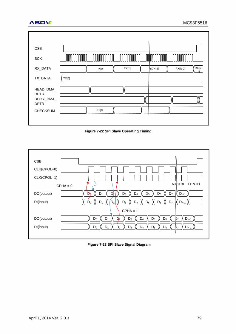
MC93F5516
April 1, 2014 Ver. 2.0.3 79
Figure 7-22 SPI Slave Operating Timing
SCK
CSB
TX_DATA
RX_DATA
HEAD_DMA_
DPTR
BODY_DMA_
DPTR
CHECKSUM
TX[0]
RX[0] RX[1] RX[N-3] RX[N-2] RX[N-
1]
RX[0]
CLK(CPOL=0)
CLK(CPOL=1)
DO(output)
DI(input)
CSB
CPHA = 0
DO(output)
DI(input)
D0 D1 D2 D3 D4 D5 D6 D7
D6 D7 D4 D5 D2 D3 D0 D1
D0 D1 D2 D3 D4 D5 D6 D7
D6 D7 D4 D5 D2 D3 D0 D1
CPHA = 1
DN-1
DN-1
DN-1
DN-1
N=8+BIT_LENTH
Figure 7-23 SPI Slave Signal Diagram
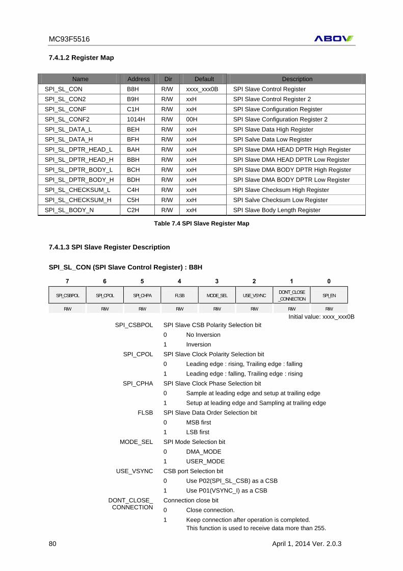
MC93F5516
80 April 1, 2014 Ver. 2.0.3
7.4.1.2 Register Map
Name Address Dir Default Description
SPI_SL_CON B8H R/W xxxx_xxx0B SPI Slave Control Register
SPI_SL_CON2 B9H R/W xxH SPI Slave Control Register 2
SPI_SL_CONF C1H R/W xxH SPI Slave Configuration Register
SPI_SL_CONF2 1014H R/W 00H SPI Slave Configuration Register 2
SPI_SL_DATA_L BEH R/W xxH SPI Slave Data High Register
SPI_SL_DATA_H BFH R/W xxH SPI Salve Data Low Register
SPI_SL_DPTR_HEAD_L BAH R/W xxH SPI Slave DMA HEAD DPTR High Register
SPI_SL_DPTR_HEAD_H BBH R/W xxH SPI Slave DMA HEAD DPTR Low Register
SPI_SL_DPTR_BODY_L BCH R/W xxH SPI Slave DMA BODY DPTR High Register
SPI_SL_DPTR_BODY_H BDH R/W xxH SPI Slave DMA BODY DPTR Low Register
SPI_SL_CHECKSUM_L C4H R/W xxH SPI Slave Checksum High Register
SPI_SL_CHECKSUM_H C5H R/W xxH SPI Salve Checksum Low Register
SPI_SL_BODY_N C2H R/W xxH SPI Slave Body Length Register
Table 7.4 SPI Slave Register Map
7.4.1.3 SPI Slave Register Description
SPI_SL_CON (SPI Slave Control Register) : B8H
7 6 5 4 3 2 1 0
SPI_CSBPOL SPI_CPOL SPI_CHPA FLSB MODE_SEL USE_VSYNC DON’T_CLOSE
_CONNECTION SPI_EN
R/W R/W R/W R/W R/W R/W R/W R/W
Initial value: xxxx_xxx0B
SPI_CSBPOL SPI Slave CSB Polarity Selection bit
0 No Inversion
1 Inversion
SPI_CPOL SPI Slave Clock Polarity Selection bit
0 Leading edge : rising, Trailing edge : falling
1 Leading edge : falling, Trailing edge : rising
SPI_CPHA SPI Slave Clock Phase Selection bit
0 Sample at leading edge and setup at trailing edge
1 Setup at leading edge and Sampling at trailing edge
FLSB SPI Slave Data Order Selection bit
0 MSB first
1 LSB first
MODE_SEL SPI Mode Selection bit
0 DMA_MODE
1 USER_MODE
USE_VSYNC CSB port Selection bit
0 Use P02(SPI_SL_CSB) as a CSB
1 Use P01(VSYNC_I) as a CSB
DONT_CLOSE_ CONNECTION
Connection close bit
0 Close connection.
1 Keep connection after operation is completed.
This function is used to receive data more than 255.
MC93F5516
April 1, 2014 Ver. 2.0.3 81
SPI_EN SPI Slave Enable bit
0 Disable
1 Enable
SPI_SL_CON2 (SPI Slave Control Register) : B9H
7 6 5 4 3 2 1 0
P12 P10 P8
R/W R/W R/W R/W R/W R/W R/W R/W
Initial value: XXH
P12 P12 packing mode
0 Disable
1 Enable
P10 P10 packing mode
0 Disable
1 Enable
P8 P8 packing mode
0 Disable
1 Enable
SPI_SL_CONF (SPI Slave Configuration Register) : C1H
7 6 5 4 3 2 1 0
CHECKSUM_TYPE - HEAD_LENGTH1 HEAD_LENGTH0 BIT_LENGth3 BIT_LENGth2 BIT_LENGth1 BIT_LENGth0
R/W R/W R/W R/W R/W R/W R/W R/W
Initial value: XXH
CHECKSUM_TYPE CEHCKSUM type
0 XOR
1 ADD
HEAD_LENGTH Byte Order Selection Bit
00 1
01 2
10 3
11 4
BIT_LENGTH 3, 2, 1, 0
SPI Slave Bit Length Selection
DIV3 DIV2 DIV1 DIV0 Description
0 0 0 0 8 Bit
0 0 0 1 9 Bit
0 0 1 0 10 Bit
0 0 1 1 11 Bit
0 1 0 0 12 Bit
0 1 0 1 13 Bit
0 1 1 0 14 Bit
0 1 1 1 15 Bit
1 0 0 0
16it
|
1 1 1 1
MC93F5516
82 April 1, 2014 Ver. 2.0.3
SPI_SL_CONF2 (SPI Slave Configuration Register2) : 1013H
7 6 5 4 3 2 1 0
- - - - SPI_SL_DB3 SPI_SL_DB2 SPI_SL_DB1 SPI_SL_DB0
- - - - R/W R/W R/W R/W
Initial value: 00H
SPI_SL_DB 3, 2, 1, 0
SPI Slave Debounce Time
Debounce Time = ((2*SPI_SL_DB)+1) * 1 system Clock
If SPI_SL_DB is 0, Debounce Time is 2.
SPI_SL_DATA_L (SPI Slave Data Low Register) : BEH
7 6 5 4 3 2 1 0
SPI_SL_DATA7 SPI_SL_DATA6 SPI_SL_DATA5 SPI_SL_DATA4 SPI_SL_DATA3 SPI_SL_DATA2 SPI_SL_DATA1 SPI_SL_DATA0
R/W R/W R/W R/W R/W R/W R/W R/W
Initial value : xxH
SPI_SL_DATA[7:0] SPI Slave Data Low Register Data
SPI_SL_DATA_H (SPI Slave Data High Register) : BFH
7 6 5 4 3 2 1 0
SPI_SL_DATA15 SPI_SL_DATA14 SPI_SL_DATA13 SPI_SL_DATA12 SPI_SL_DATA11 SPI_SL_DATA10 SPI_SL_DATA9 SPI_SL_DATA8
R/W R/W R/W R/W R/W R/W R/W R/W
Initial value : xxH
SPI_SL_DATA[15:8] SPI Slave Data High Register Data
SPI_SL_DPTR_HEAD_L (SPI Slave DPTR Head Low Register) : BAH
7 6 5 4 3 2 1 0
DPTR_SL
_HEAD7
DPTR_SL
_HEAD6
DPTR_SL
_HEAD5
DPTR_SL
_HEAD4
DPTR_SL
_HEAD3
DPTR_SL
_HEAD2
DPTR_SL
_HEAD1
DPTR_SL
_HEAD0
R/W R/W R/W R/W R/W R/W R/W R/W
Initial value : xxH
DPTR_SL_HEAD[7:0] SPI Slave DMA Head Data Pointer LSB
SPI_SL_DPTR_HEAD_H (SPI Slave DPTR Head High Register) : BBH
7 6 5 4 3 2 1 0
DPTR_SL
_HEAD15
DPTR_SL
_HEAD14
DPTR_SL
_HEAD13
DPTR_SL
_HEAD12
DPTR_SL
_HEAD11
DPTR_SL
_HEAD10
DPTR_SL
_HEAD9
DPTR_SL
_HEAD8
R/W R/W R/W R/W R/W R/W R/W R/W
Initial value : xxH
DPTR_SL_HEAD[15:8] SPI Slave DMA Head Data Pointer MSB
SPI_SL_DPTR_BODY_L (SPI Slave DPTR Body Low Register) : BCH
7 6 5 4 3 2 1 0
DPTR_SL
_BODY7
DPTR_SL _
BODY6
DPTR_SL _ BODY
5
DPTR_SL _ BODY
4
DPTR_SL _ BODY
3
DPTR_SL _ BODY
2
DPTR_SL _ BODY
1
DPTR_SL _ BODY
0
R/W R/W R/W R/W R/W R/W R/W R/W
Initial value : xxH
DPTR_SL_BODY[7:0] SPI Slave DMA Body Data Pointer LSB
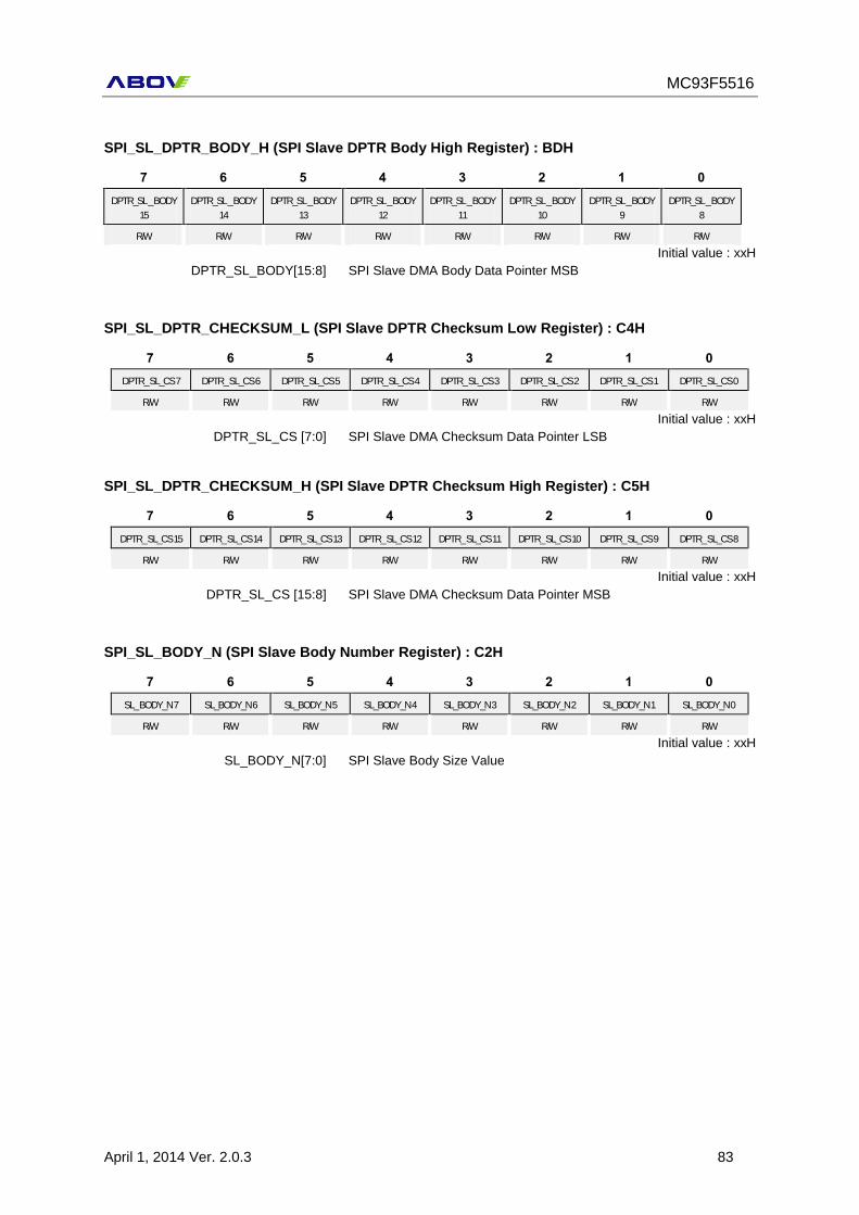
MC93F5516
April 1, 2014 Ver. 2.0.3 83
SPI_SL_DPTR_BODY_H (SPI Slave DPTR Body High Register) : BDH
7 6 5 4 3 2 1 0
DPTR_SL _ BODY
15
DPTR_SL _ BODY
14
DPTR_SL _ BODY
13
DPTR_SL _ BODY
12
DPTR_SL _ BODY
11
DPTR_SL _ BODY
10
DPTR_SL _ BODY
9
DPTR_SL _ BODY
8
R/W R/W R/W R/W R/W R/W R/W R/W
Initial value : xxH
DPTR_SL_BODY[15:8] SPI Slave DMA Body Data Pointer MSB
SPI_SL_DPTR_CHECKSUM_L (SPI Slave DPTR Checksum Low Register) : C4H
7 6 5 4 3 2 1 0
DPTR_ SL_CS 7 DPTR_ SL_CS 6 DPTR_ SL_CS 5 DPTR_ SL_CS 4 DPTR_ SL_CS 3 DPTR_ SL_CS 2 DPTR_ SL_CS 1 DPTR_ SL_CS 0
R/W R/W R/W R/W R/W R/W R/W R/W
Initial value : xxH
DPTR_SL_CS [7:0] SPI Slave DMA Checksum Data Pointer LSB
SPI_SL_DPTR_CHECKSUM_H (SPI Slave DPTR Checksum High Register) : C5H
7 6 5 4 3 2 1 0
DPTR_ SL_CS 15 DPTR_ SL_CS 14 DPTR_ SL_CS 13 DPTR_ SL_CS 12 DPTR_ SL_CS 11 DPTR_ SL_CS 10 DPTR_ SL_CS 9 DPTR_ SL_CS 8
R/W R/W R/W R/W R/W R/W R/W R/W
Initial value : xxH
DPTR_SL_CS [15:8] SPI Slave DMA Checksum Data Pointer MSB
SPI_SL_BODY_N (SPI Slave Body Number Register) : C2H
7 6 5 4 3 2 1 0
SL_ BODY_N 7 SL_BODY_N 6 SL_BODY_N 5 SL_BODY_N 4 SL_BODY_N 3 SL_BODY_N 2 SL_BODY_N 1 SL_BODY_N 0
R/W R/W R/W R/W R/W R/W R/W R/W
Initial value : xxH
SL_BODY_N[7:0] SPI Slave Body Size Value
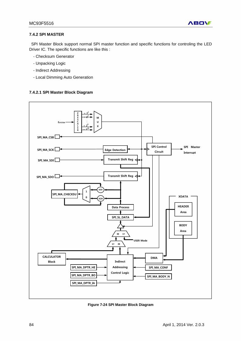
MC93F5516
84 April 1, 2014 Ver. 2.0.3
7.4.2 SPI MASTER
SPI Master Block support normal SPI master function and specific functions for controling the LED
Driver IC. The specific functions are like this :
- Checksum Generator
- Unpacking Logic
- Indirect Addressing
- Local Dimming Auto Generation
7.4.2.1 SPI Master Block Diagram
Figure 7-24 SPI Master Block Diagram
Edge Detection SPI Control
Circuit SPI_MA_SCK
SPI_MA_SDI
SPI_MA_SDO
SPI Master
Interrupt
SPI_MA_CSB
ADD
XOR
1
0
SPI_SL_DATA
M
U
X
Transmit Shift Reg
÷ 21
÷ 22
÷ 29
÷ 210
Data Process
HEADER
Area
BODY
Area
XDATA
Indirect
Addressing
Control Logic
SPI_MA_DPTR_HE
SPI_MA_DPTR_BO
SPI_MA_DPTR_IA
CALCULATOR
Block
DMA
SPI_MA_CONF
fSYSTEM
P R E S C A L E R
Transmit Shift Reg
USER Mode
1 0 0 1
SPI_MA_CHECKSU
M
SPI_MA_BODY_N
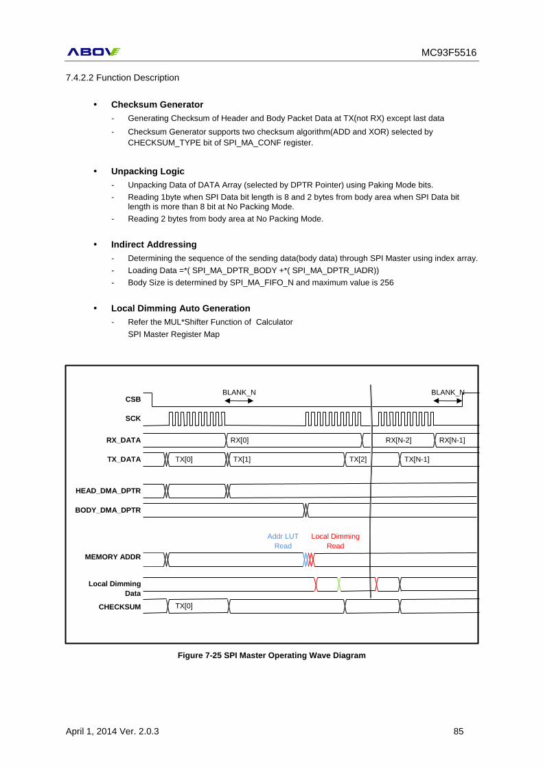
MC93F5516
April 1, 2014 Ver. 2.0.3 85
7.4.2.2 Function Description
Checksum Generator
- Generating Checksum of Header and Body Packet Data at TX(not RX) except last data
- Checksum Generator supports two checksum algorithm(ADD and XOR) selected by
CHECKSUM_TYPE bit of SPI_MA_CONF register.
Unpacking Logic
- Unpacking Data of DATA Array (selected by DPTR Pointer) using Paking Mode bits.
- Reading 1byte when SPI Data bit length is 8 and 2 bytes from body area when SPI Data bit length is more than 8 bit at No Packing Mode.
- Reading 2 bytes from body area at No Packing Mode.
Indirect Addressing
- Determining the sequence of the sending data(body data) through SPI Master using index array.
- Loading Data =*( SPI_MA_DPTR_BODY +*( SPI_MA_DPTR_IADR))
- Body Size is determined by SPI_MA_FIFO_N and maximum value is 256
Local Dimming Auto Generation
- Refer the MUL*Shifter Function of Calculator
SPI Master Register Map
Figure 7-25 SPI Master Operating Wave Diagram
TX[0]
RX[0] RX[N-2] RX[N-1]
Addr LUT
Read
TX[1] TX[2] TX[N-1]
BLANK_N BLANK_N
Local Dimming
Read
TX[0]
SCK
CSB
TX_DATA
RX_DATA
HEAD_DMA_DPTR
BODY_DMA_DPTR
MEMORY ADDR
Local Dimming
Data
CHECKSUM
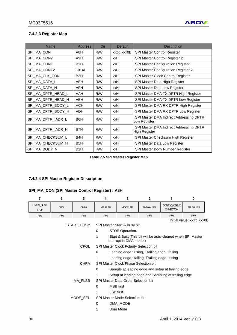
MC93F5516
86 April 1, 2014 Ver. 2.0.3
7.4.2.3 Register Map
Name Address Dir Default Description
SPI_MA_CON A8H R/W xxxx_xxx0B SPI Master Control Register
SPI_MA_CON2 A9H R/W xxH SPI Master Control Register 2
SPI_MA_CONF B1H R/W xxH SPI Master Configuration Register
SPI_MA_CONF2 1014H R/W xxH SPI Master Configuration Register 2
SPI_MA_CLK_CON B3H R/W xxH SPI Master Clock Control Register
SPI_MA_DATA_L AEH R/W xxH SPI Master Data High Register
SPI_MA_DATA_H AFH R/W xxH SPI Master Data Low Register
SPI_MA_DPTR_HEAD_L AAH R/W xxH SPI Master DMA TX DPTR High Register
SPI_MA_DPTR_HEAD_H ABH R/W xxH SPI Master DMA TX DPTR Low Register
SPI_MA_DPTR_BODY_L ACH R/W xxH SPI Master DMA RX DPTR High Register
SPI_MA_DPTR_BODY_H ADH R/W xxH SPI Master DMA RX DPTR Low Register
SPI_MA_DPTR_IADR_L B6H R/W xxH SPI Master DMA Indirect Addressing DPTR
Low Register
SPI_MA_DPTR_IADR_H B7H R/W xxH SPI Master DMA Indirect Addressing DPTR
High Register
SPI_MA_CHECKSUM_L B4H R/W xxH SPI Master Checksum High Register
SPI_MA_CHECKSUM_H B5H R/W xxH SPI Master Data Low Register
SPI_MA_BODY_N B2H R/W xxH SPI Master Body Number Register
Table 7.5 SPI Master Register Map
7.4.2.4 SPI Master Register Description
SPI_MA_CON (SPI Master Control Register) : A8H
7 6 5 4 3 2 1 0
START_BUSY
STOP CPOL CHPA MA_FLSB MODE_SEL ENDIAN_SEL
DON’T_CLOSE_C
ONNECTION SPI_MA_EN
R/W R/W R/W R/W R/W R/W R/W R/W
Initial value: xxxx_xxx0B
START_BUSY SPI Master Start & Busy bit
0 STOP Operation.
1 Start & Busy(This bit will be auto-cleared when SPI Master interrupt in DMA mode.)
CPOL SPI Master Clock Polarity Selection bit
0 Leading edge : rising, Trailing edge : falling
1 Leading edge : falling, Trailing edge : rising
CHPA SPI Master Clock Phase Selection bit
0 Sample at leading edge and setup at trailing edge
1 Setup at leading edge and Sampling at trailing edge
MA_FLSB SPI Master Data Order Selection bit
0 MSB first
1 LSB first
MODE_SEL SPI Master Mode Selection bit
0 DMA_MODE
1 User Mode
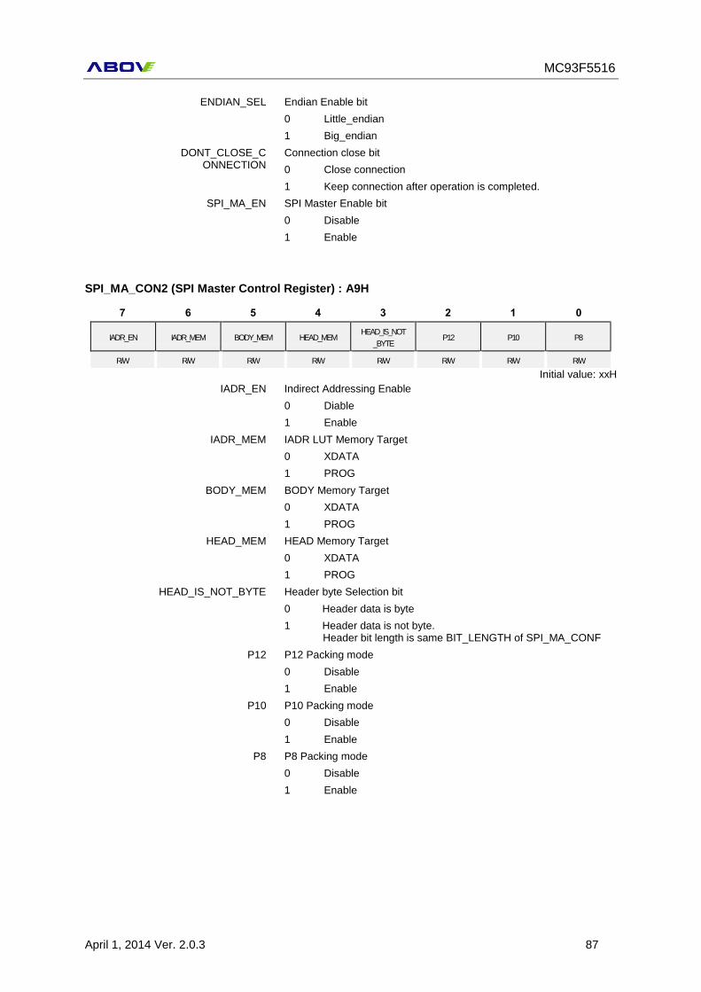
MC93F5516
April 1, 2014 Ver. 2.0.3 87
ENDIAN_SEL Endian Enable bit
0 Little_endian
1 Big_endian
DONT_CLOSE_CONNECTION
Connection close bit
0 Close connection
1 Keep connection after operation is completed.
SPI_MA_EN SPI Master Enable bit
0 Disable
1 Enable
SPI_MA_CON2 (SPI Master Control Register) : A9H
7 6 5 4 3 2 1 0
IADR_EN IADR_MEM BODY_MEM HEAD_MEM HEAD_IS_NOT
_BYTE P12 P10 P8
R/W R/W R/W R/W R/W R/W R/W R/W
Initial value: xxH
IADR_EN Indirect Addressing Enable
0 Diable
1 Enable
IADR_MEM IADR LUT Memory Target
0 XDATA
1 PROG
BODY_MEM BODY Memory Target
0 XDATA
1 PROG
HEAD_MEM HEAD Memory Target
0 XDATA
1 PROG
HEAD_IS_NOT_BYTE Header byte Selection bit
0 Header data is byte
1 Header data is not byte. Header bit length is same BIT_LENGTH of SPI_MA_CONF
P12 P12 Packing mode
0 Disable
1 Enable
P10 P10 Packing mode
0 Disable
1 Enable
P8 P8 Packing mode
0 Disable
1 Enable

MC93F5516
88 April 1, 2014 Ver. 2.0.3
SPI_MA_CONF (SPI Master Configuration Register) : B1H
7 6 5 4 3 2 1 0
CHECKSUM_TYPE - HEAD_LENGTH1 HEAD_LENGTH0 BIT_LENGth3 BIT_LENGth2 BIT_LENGth1 BIT_LENGth0
R/W R/W R/W R/W R/W R/W R/W R/W
Initial value: xxH
CHECKSUM_TYPE CEHCKSUM type
0 XOR
1 ADD
HEAD_LENGTH Byte Order Selection Bit
00 1
01 2
10 3
11 4
BIT_LENGTH 3, 2, 1, 0
SPI Slave Bit Length Selection
DIV3 DIV2 DIV1 DIV0 Description
0 0 0 0 8 Bit
0 0 0 1 9 Bit
0 0 1 0 10 Bit
0 0 1 1 11 Bit
0 1 0 0 12 Bit
0 1 0 1 13 Bit
0 1 1 0 14 Bit
0 1 1 1 15 Bit
1 0 0 0
16it
1 0 0 1
1 0 1 0
1 0 1 1
1 1 0 0
1 1 0 1
1 1 1 0
1 1 1 1
SPI_MA_CONF2 (SPI Master Configuration Register 2) : 1014H
7 6 5 4 3 2 1 0
- - - INVERSIONB SPI_MA_DB3 SPI_MA_DB2 SPI_MA_DB1 SPI_MA_DB0
- - - - R/W R/W R/W R/W
Initial value: XXH
INVERSIONB SPI Master Tx Data Inversion bit
SPI_MA_DB 3, 2, 1, 0
SPI Master Debounce Time
Debounce Time = ((2*SPI_MA_DB)+1) * 1 system Clock
If SPI_MA_DB is 0, Debounce Time is 2.
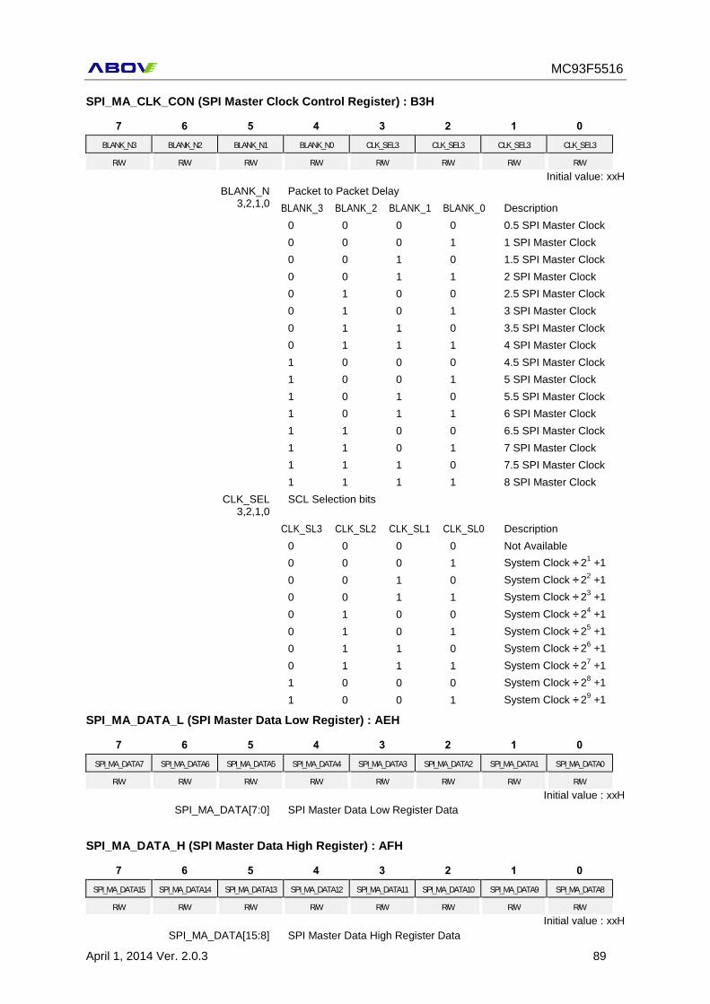
MC93F5516
April 1, 2014 Ver. 2.0.3 89
SPI_MA_CLK_CON (SPI Master Clock Control Register) : B3H
7 6 5 4 3 2 1 0
BLANK_N3 BLANK_N2 BLANK_N1 BLANK_N0 CLK_SEL3 CLK_SEL3 CLK_SEL3 CLK_SEL3
R/W R/W R/W R/W R/W R/W R/W R/W
Initial value: xxH
BLANK_N 3,2,1,0
Packet to Packet Delay
BLANK_3 BLANK_2 BLANK_1 BLANK_0 Description
0 0 0 0 0.5 SPI Master Clock
0 0 0 1 1 SPI Master Clock
0 0 1 0 1.5 SPI Master Clock
0 0 1 1 2 SPI Master Clock
0 1 0 0 2.5 SPI Master Clock
0 1 0 1 3 SPI Master Clock
0 1 1 0 3.5 SPI Master Clock
0 1 1 1 4 SPI Master Clock
1 0 0 0 4.5 SPI Master Clock
1 0 0 1 5 SPI Master Clock
1 0 1 0 5.5 SPI Master Clock
1 0 1 1 6 SPI Master Clock
1 1 0 0 6.5 SPI Master Clock
1 1 0 1 7 SPI Master Clock
1 1 1 0 7.5 SPI Master Clock
1 1 1 1 8 SPI Master Clock
CLK_SEL 3,2,1,0
SCL Selection bits
CLK_SL3 CLK_SL2 CLK_SL1 CLK_SL0 Description
0 0 0 0 Not Available
0 0 0 1 System Clock ÷ 21 +1
0 0 1 0 System Clock ÷ 22 +1
0 0 1 1 System Clock ÷ 23 +1
0 1 0 0 System Clock ÷ 24 +1
0 1 0 1 System Clock ÷ 25 +1
0 1 1 0 System Clock ÷ 26 +1
0 1 1 1 System Clock ÷ 27 +1
1 0 0 0 System Clock ÷ 28 +1
1 0 0 1 System Clock ÷ 29 +1
SPI_MA_DATA_L (SPI Master Data Low Register) : AEH
7 6 5 4 3 2 1 0
SPI_MA_DATA7 SPI_MA_DATA6 SPI_MA_DATA5 SPI_MA_DATA4 SPI_MA_DATA3 SPI_MA_DATA2 SPI_MA_DATA1 SPI_MA_DATA0
R/W R/W R/W R/W R/W R/W R/W R/W
Initial value : xxH
SPI_MA_DATA[7:0] SPI Master Data Low Register Data
SPI_MA_DATA_H (SPI Master Data High Register) : AFH
7 6 5 4 3 2 1 0
SPI_MA_DATA15 SPI_MA_DATA14 SPI_MA_DATA13 SPI_MA_DATA12 SPI_MA_DATA11 SPI_MA_DATA10 SPI_MA_DATA9 SPI_MA_DATA8
R/W R/W R/W R/W R/W R/W R/W R/W
Initial value : xxH
SPI_MA_DATA[15:8] SPI Master Data High Register Data
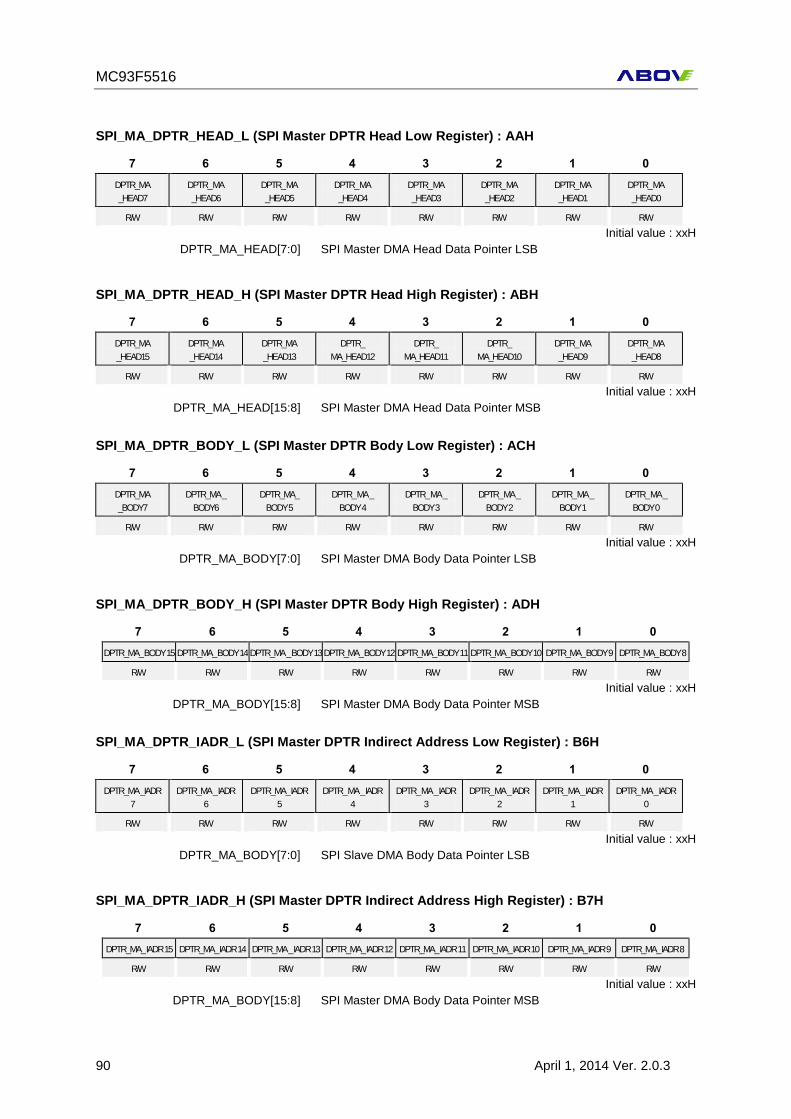
MC93F5516
90 April 1, 2014 Ver. 2.0.3
SPI_MA_DPTR_HEAD_L (SPI Master DPTR Head Low Register) : AAH
7 6 5 4 3 2 1 0
DPTR_MA
_HEAD7
DPTR_ MA
_HEAD6
DPTR_ MA
_HEAD5
DPTR_ MA
_HEAD4
DPTR_ MA
_HEAD3
DPTR_ MA
_HEAD2
DPTR_ MA
_HEAD1
DPTR_ MA
_HEAD0
R/W R/W R/W R/W R/W R/W R/W R/W
Initial value : xxH
DPTR_MA_HEAD[7:0] SPI Master DMA Head Data Pointer LSB
SPI_MA_DPTR_HEAD_H (SPI Master DPTR Head High Register) : ABH
7 6 5 4 3 2 1 0
DPTR_MA
_HEAD15
DPTR_MA
_HEAD14
DPTR_MA
_HEAD13
DPTR_
MA_HEAD12
DPTR_
MA_HEAD11
DPTR_
MA_HEAD10
DPTR_ MA
_HEAD9
DPTR_ MA
_HEAD8
R/W R/W R/W R/W R/W R/W R/W R/W
Initial value : xxH
DPTR_MA_HEAD[15:8] SPI Master DMA Head Data Pointer MSB
SPI_MA_DPTR_BODY_L (SPI Master DPTR Body Low Register) : ACH
7 6 5 4 3 2 1 0
DPTR_MA
_BODY7
DPTR_MA _
BODY6
DPTR_MA_
BODY 5
DPTR_ MA _
BODY 4
DPTR_ MA _
BODY 3
DPTR_ MA _
BODY 2
DPTR_ MA _
BODY 1
DPTR_ MA _
BODY 0
R/W R/W R/W R/W R/W R/W R/W R/W
Initial value : xxH
DPTR_MA_BODY[7:0] SPI Master DMA Body Data Pointer LSB
SPI_MA_DPTR_BODY_H (SPI Master DPTR Body High Register) : ADH
7 6 5 4 3 2 1 0
DPTR_MA_ BODY 15 DPTR_MA_ BODY 14 DPTR_MA _ BODY 13 DPTR_MA_ BODY 12 DPTR_MA_ BODY 11 DPTR_MA_ BODY 10 DPTR_MA_ BODY 9 DPTR_MA_ BODY 8
R/W R/W R/W R/W R/W R/W R/W R/W
Initial value : xxH
DPTR_MA_BODY[15:8] SPI Master DMA Body Data Pointer MSB
SPI_MA_DPTR_IADR_L (SPI Master DPTR Indirect Address Low Register) : B6H
7 6 5 4 3 2 1 0
DPTR_MA _IADR
7
DPTR_MA _ IADR
6
DPTR_MA_ IADR
5
DPTR_ MA _ IADR
4
DPTR_ MA _ IADR
3
DPTR_ MA _ IADR
2
DPTR_ MA _ IADR
1
DPTR_ MA _ IADR
0
R/W R/W R/W R/W R/W R/W R/W R/W
Initial value : xxH
DPTR_MA_BODY[7:0] SPI Slave DMA Body Data Pointer LSB
SPI_MA_DPTR_IADR_H (SPI Master DPTR Indirect Address High Register) : B7H
7 6 5 4 3 2 1 0
DPTR_MA_ IADR 15 DPTR_MA_ IADR 14 DPTR_MA _ IADR 13 DPTR_MA_ IADR 12 DPTR_MA_ IADR 11 DPTR_MA_ IADR 10 DPTR_MA_ IADR 9 DPTR_MA_ IADR 8
R/W R/W R/W R/W R/W R/W R/W R/W
Initial value : xxH
DPTR_MA_BODY[15:8] SPI Master DMA Body Data Pointer MSB
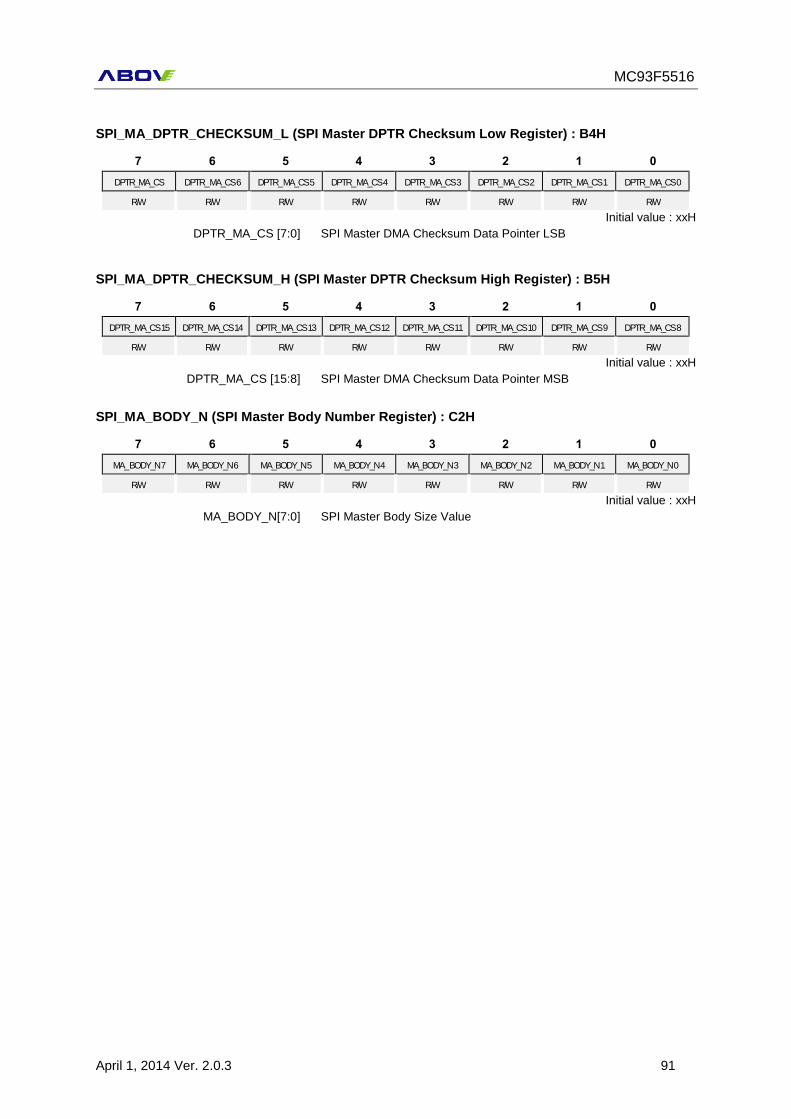
MC93F5516
April 1, 2014 Ver. 2.0.3 91
SPI_MA_DPTR_CHECKSUM_L (SPI Master DPTR Checksum Low Register) : B4H
7 6 5 4 3 2 1 0
DPTR_MA_CS DPTR_ MA_CS 6 DPTR_ MA_CS 5 DPTR_ MA_CS 4 DPTR_ MA_CS 3 DPTR_ MA_CS 2 DPTR_ MA_CS 1 DPTR_ MA_CS 0
R/W R/W R/W R/W R/W R/W R/W R/W
Initial value : xxH
DPTR_MA_CS [7:0] SPI Master DMA Checksum Data Pointer LSB
SPI_MA_DPTR_CHECKSUM_H (SPI Master DPTR Checksum High Register) : B5H
7 6 5 4 3 2 1 0
DPTR_ MA_CS 15 DPTR_ MA_CS 14 DPTR_ MA_CS 13 DPTR_ MA_CS 12 DPTR_ MA_CS 11 DPTR_ MA_CS 10 DPTR_ MA_CS 9 DPTR_ MA_CS 8
R/W R/W R/W R/W R/W R/W R/W R/W
Initial value : xxH
DPTR_MA_CS [15:8] SPI Master DMA Checksum Data Pointer MSB
SPI_MA_BODY_N (SPI Master Body Number Register) : C2H
7 6 5 4 3 2 1 0
MA_ BODY_N 7 MA_BODY_N 6 MA_BODY_N 5 MA_BODY_N 4 MA_BODY_N 3 MA_BODY_N 2 MA_BODY_N 1 MA_BODY_N 0
R/W R/W R/W R/W R/W R/W R/W R/W
Initial value : xxH
MA_BODY_N[7:0] SPI Master Body Size Value
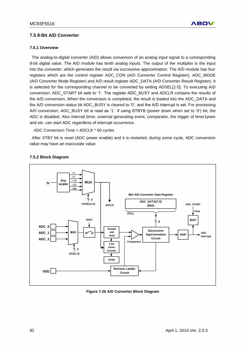
MC93F5516
92 April 1, 2014 Ver. 2.0.3
7.5 8-Bit A/D Converter
7.5.1 Overview
The analog-to-digital converter (A/D) allows conversion of an analog input signal to a corresponding
8-bit digital value. The A/D module has tenth analog inputs. The output of the multiplex is the input
into the converter, which generates the result via successive approximation. The A/D module has four
registers which are the control register ADC_CON (A/D Converter Control Register), ADC_MODE
(A/D Converter Mode Register) and A/D result register ADC_DATA (A/D Converter Result Register). It
is selected for the corresponding channel to be converted by setting ADSEL[1:0]. To executing A/D
conversion, ADC_START bit sets to ‘1’. The register ADC_BUSY and ADCLR contains the results of
the A/D conversion. When the conversion is completed, the result is loaded into the ADC_DATA and
the A/D conversion status bit ADC_BUSY is cleared to ‘0’, and the A/D interrupt is set. For processing
A/D conversion, ADC_BUSY bit is read as ‘1’. If using STBYB (power down when set to ‘0’) bit, the
ADC is disabled. Also internal timer, external generating event, comparator, the trigger of timer1pwm
and etc. can start ADC regardless of interrupt occurrence.
ADC Conversion Time = ADCLK * 60 cycles
After STBY bit is reset (ADC power enable) and it is restarted, during some cycle, ADC conversion
value may have an inaccurate value.
7.5.2 Block Diagram
Figure 7-26 A/D Converter Block Diagram
ADC_1
ADC_2
Successive
Approximation
Circuit
ADIF
ADC_DATA[7:0]
(8bit)
Resistor Ladder
Circuit VDD
8bit A/D Converter Data Register
ADS[1:0]
2
8
ADC
Interrupt
Pre scaler
MUX
÷4
÷8
÷16
÷32 fx
CKSEL[1:0]
2
ADC_START
Clear
Comparator
[FDH]
ADCLK
ADST
ADC_0
÷64
Sample
and
Hold
4 bit
Down
Counter
STDR
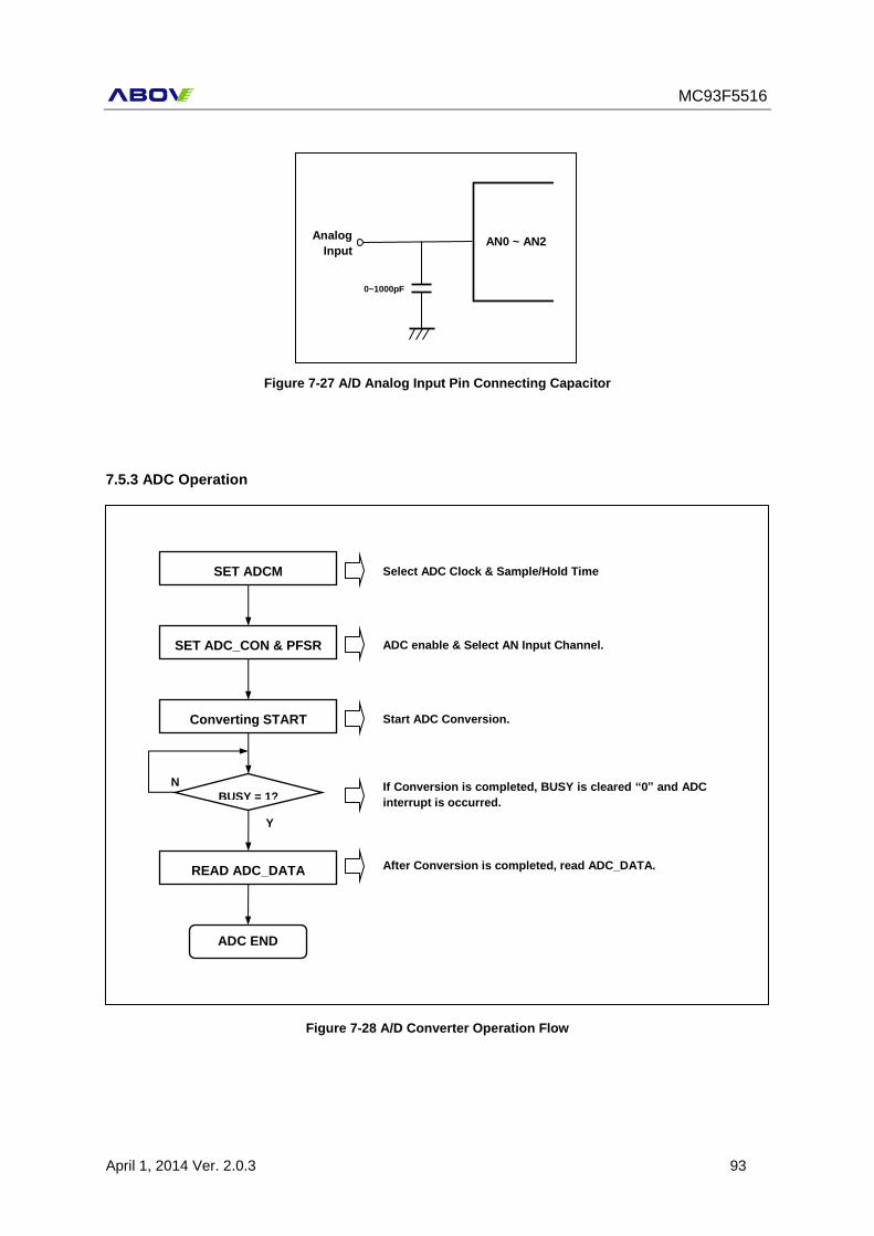
MC93F5516
April 1, 2014 Ver. 2.0.3 93
Figure 7-27 A/D Analog Input Pin Connecting Capacitor
7.5.3 ADC Operation
Figure 7-66 A/D Converter Operation Flow
0~1000pF
AN0 ~ AN2 Analog
Input
SET ADCM
SET ADC_CON & PFSR
BUSY = 1?
Converting START
READ ADC_DATA
ADC END
Select ADC Clock & Sample/Hold Time
ADC enable & Select AN Input Channel.
Start ADC Conversion.
If Conversion is completed, BUSY is cleared “0” and ADC
interrupt is occurred.
After Conversion is completed, read ADC_DATA.
Y
N
Figure 7-28 A/D Converter Operation Flow
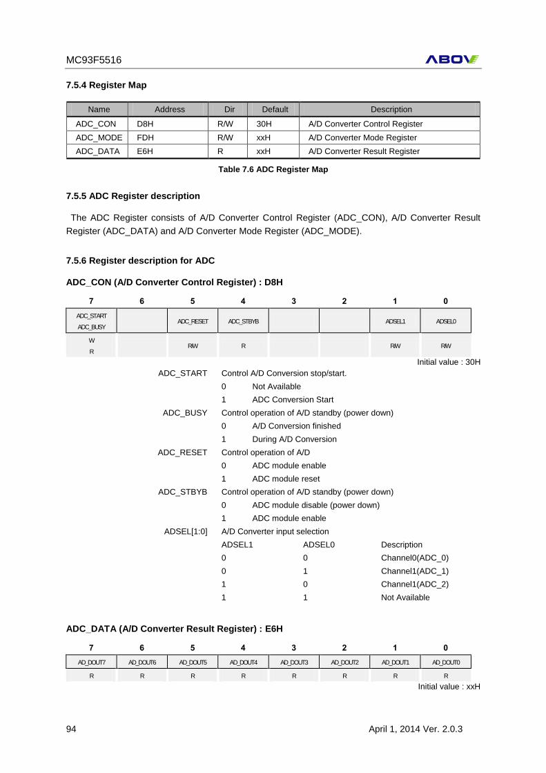
MC93F5516
94 April 1, 2014 Ver. 2.0.3
7.5.4 Register Map
Name Address Dir Default Description
ADC_CON D8H R/W 30H A/D Converter Control Register
ADC_MODE FDH R/W xxH A/D Converter Mode Register
ADC_DATA E6H R xxH A/D Converter Result Register
Table 7.6 ADC Register Map
7.5.5 ADC Register description
The ADC Register consists of A/D Converter Control Register (ADC_CON), A/D Converter Result
Register (ADC_DATA) and A/D Converter Mode Register (ADC_MODE).
7.5.6 Register description for ADC
ADC_CON (A/D Converter Control Register) : D8H
7 6 5 4 3 2 1 0
ADC_START
ADC_BUSY ADC_RESET ADC_STBYB ADSEL1 ADSEL0
W
R R/W R R/W R/W
Initial value : 30H
ADC_START Control A/D Conversion stop/start.
0 Not Available
1 ADC Conversion Start
ADC_BUSY Control operation of A/D standby (power down)
0 A/D Conversion finished
1 During A/D Conversion
ADC_RESET Control operation of A/D
0 ADC module enable
1 ADC module reset
ADC_STBYB Control operation of A/D standby (power down)
0 ADC module disable (power down)
1 ADC module enable
ADSEL[1:0] A/D Converter input selection
ADSEL1 ADSEL0 Description
0 0 Channel0(ADC_0)
0 1 Channel1(ADC_1)
1 0 Channel1(ADC_2)
1 1 Not Available
ADC_DATA (A/D Converter Result Register) : E6H
7 6 5 4 3 2 1 0
AD_DOUT7 AD_DOUT6 AD_DOUT5 AD_DOUT4 AD_DOUT3 AD_DOUT2 AD_DOUT1 AD_DOUT0
R R R R R R R R
Initial value : xxH
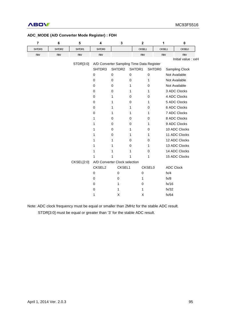
MC93F5516
April 1, 2014 Ver. 2.0.3 95
ADC_MODE (A/D Converter Mode Register) : FDH
7 6 5 4 3 2 1 0
SHTDR3 SHTDR2 SHTDR1 SHTDR0 CKSEL1 CKSEL1 CKSEL0
R/W R/W R/W R/W R/W R/W R/W
Initial value : xxH
STDR[3:0] A/D Converter Sampling Time Data Register
SHTDR3 SHTDR2 SHTDR1 SHTDR0 Sampling Clock
0 0 0 0 Not Available
0 0 0 1 Not Available
0 0 1 0 Not Available
0 0 1 1 3 ADC Clocks
0 1 0 0 4 ADC Clocks
0 1 0 1 5 ADC Clocks
0 1 1 0 6 ADC Clocks
0 1 1 1 7 ADC Clocks
1 0 0 0 8 ADC Clocks
1 0 0 1 9 ADC Clocks
1 0 1 0 10 ADC Clocks
1 0 1 1 11 ADC Clocks
1 1 0 0 12 ADC Clocks
1 1 0 1 13 ADC Clocks
1 1 1 0 14 ADC Clocks
1 1 1 1 15 ADC Clocks
CKSEL[2:0] A/D Converter Clock selection
CKSEL2 CKSEL1 CKSEL0 ADC Clock
0 0 0 fx/4
0 0 1 fx/8
0 1 0 fx/16
0 1 1 fx/32
1 X X fx/64
Note: ADC clock frequency must be equal or smaller than 2MHz for the stable ADC result.
STDR[3:0] must be equal or greater than ‘3’ for the stable ADC result.
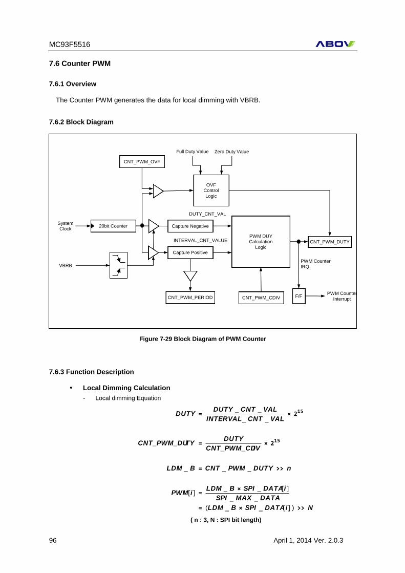
MC93F5516
96 April 1, 2014 Ver. 2.0.3
7.6 Counter PWM
7.6.1 Overview
The Counter PWM generates the data for local dimming with VBRB.
7.6.2 Block Diagram
Figure 7-29 Block Diagram of PWM Counter
7.6.3 Function Description
Local Dimming Calculation
- Local dimming Equation
NiDATASPIBLDM
DATAMAXSPI
iDATASPIBLDMiPWM
nDUTYPWMCNTBLDM
IVCNT_PWM_CD
DUTYTYCNT_PWM_DU
VALCNTINTERVAL
VALCNTDUTYDUTY
>>×=
×=
>>=
2×=
2×=
15
15
])[__(
__
][__][
___
__
__
( n : 3, N : SPI bit length)
VBRB
System Clock
CNT_PWM_DUTY
OVF Control
Logic
Full Duty Value Zero Duty Value
20bit Counter Capture Negative
Capture Positive
CNT_PWM_CDIV
CNT_PWM_OVF
INTERVAL_CNT_VALUE
DUTY_CNT_VAL
CNT_PWM_PERIOD
PWM Counter IRQ
F/F PWM Counter
Interrupt
PWM DUY Calculation
Logic

MC93F5516
April 1, 2014 Ver. 2.0.3 97
- CNT_PWM_CDIV Table
SPI bit CNT_PWM_CDIV remarks
8bit 32633
9bit 32697
10bit 32729
11bit 32745
12bit 32768
Table 7.7 CNT_PWM_CDIV Table
Overflow Operation
- When 20bit_counter value is more than CNT_PWM_OVF, overflow operation is triggered.
- VBRB Input is HIGH : CNT_PWM_DUTY = 0x8000/CUSTOM_DIV(Full Duty Value)
- VBRB Input is LOW : CNT_PWM_DUTY = 0x0000(Zero Duty Value)
- User must ignore the first data after full duty.
Reading the Period
- When READ_CDIV bit of CNT_PWM_CON register is 0, you can read the period using CNT_PWM_CDIV register.
- The period data is not 20-bit but MSB 16-bit.
Figure 7-30 Counter PWM Operating Wave Diagram
CLK
PWD
COUNTER
HIGH
INT_REQ
PERIOD
DUTY/CDIV
0
capture & restart
0
capture & restart
PERIOD PERIOD
0 HIGH
XXXX DUTY/CDIV
capture
MC93F5516
98 April 1, 2014 Ver. 2.0.3
7.6.3.1 Register Map
Name Address Dir Default Description
CNT_PWM_CON 88H R/W xxxx_xxx0B PWM Counter Controller
CNT_PWM_OVF_L 8BH R/W XXH Overflow Counter Low
CNT_PWM_OVF_M 8CH R/W XXH Overflow Counter Middle
CNT_PWM_OVF_H 8DH R/W XXH Overflow Counter High
CNT_PWM_DUTY_L 8EH R/W XXH PWM Duty Register Low
CNT_PWM_DUTY_H 8FH R/W XXH PWM Duty Register High
CNT_PWM_CDIV_L 89H R/W XXH PWM Custom Divider Low
CNT_PWM_PERIOD_L 89H R XXH PWM Period Low(4 bit right shifted)
CNT_PWM_CDIV_H 8AH R/W XXH PWM Custom Divider High
CNT_PWM_PERIOD_H 8AH R XXH PWM Period High(4 bit right shifted)
PWM_DB 1010H R/W xxH PWM Counter Debounce Register
Table 7.8 Counter PWM Register Map
7.6.3.2 Counter Register Description
CNT_PWM_CON (PWM Counter Control Register) : 88H
7 6 5 4 3 2 1 0
WCOL READ_CDIV EDGE_REF CNT_EN
R/W R/W R/W R/W
Initial value : XXXX_XXX0B
WCOL Write Collision Flag
0 Write Collision doesn’t occur.
1 Write Collision occurs. (cleared by status read).
READ_CDIV (D9H,DAH)CDIV/PERIOD selction
0 PERIOD
1 CDIV
EDGE_REF Reference Edge Selection bit
0 Negative Edge
1 Positive Edge
CNT_EN Counter Enable bit
0 Disable
1 Enable
CNT_PWM_OVF_L (Counter PWM Overflow Low Register) : 8BH
7 6 5 4 3 2 1 0
CNT_PWM_OVF 7 CNT_PWM_OVF 6 CNT_PWM_OVF 5 CNT_PWM_OVF 4 CNT_PWM_OVF 3 CNT_PWM_OVF 2 CNT_PWM_OVF 1 CNT_PWM_OVF 0
R/W R/W R/W R/W R/W R/W R/W R/W
Initial value : xxH
CNT_PWM_OVF [7:0] Counter PWM Overflow Low Register Value
MC93F5516
April 1, 2014 Ver. 2.0.3 99
CNT_PWM_OVF_M (Counter PWM Overflow Middle Register) : 8CH
7 6 5 4 3 2 1 0
CNT_PWM_OVF 15 CNT_PWM_OVF 14 CNT_PWM_OVF 13 CNT_PWM_OVF 12 CNT_PWM_OVF 11 CNT_PWM_OVF 10 CNT_PWM_OVF 9 CNT_PWM_OVF 8
R/W R/W R/W R/W R/W R/W R/W R/W
Initial value : xxH
CNT_PWM_OVF [15:8] Counter PWM Overflow Middle Register Value
CNT_PWM_OVF_H (Counter PWM Overflow High Register) : 8DH
7 6 5 4 3 2 1 0
- - - - CNT_PWM_OVF 19 CNT_PWM_OVF 18 CNT_PWM_OVF 17 CNT_PWM_OVF 16
- - - - R/W R/W R/W R/W
Initial value : xxH
CNT_PWM_OVF [19:16]
Counter PWM Overflow High Register Value
CNT_PWM_DUTY_L (Counter PWM DUTY Low Register) : 8EH
7 6 5 4 3 2 1 0
CNT_PWM_DUTY 7 CNT_PWM_DUTY 6 CNT_PWM_DUTY 5 CNT_PWM_DUTY 4 CNT_PWM_DUTY 3 CNT_PWM_DUTY 2 CNT_PWM_ DUTY 1 CNT_PWM_DUTY 0
R/W R/W R/W R/W R/W R/W R/W R/W
Initial value : xxH
CNT_PWM_DUTY [7:0]
Counter PWM Duty Low Register Value
CNT_PWM_DUTY_H (Counter PWM DUTY High Register) : 8FH
7 6 5 4 3 2 1 0
CNT_PWM_DUTY 15 CNT_PWM_DUTY 14 CNT_PWM_DUTY 13 CNT_PWM_DUTY 12 CNT_PWM_DUTY 11 CNT_PWM_DUTY 10 CNT_PWM_DUTY 9 CNT_PWM_DUTY 8
R/W R/W R/W R/W R/W R/W R/W R/W
Initial value : xxH
CNT_PWM_DUTY [15:8]
Counter PWM Duty High Register Value
CNT_PWM_CDIV_L (Counter PWM CDIV Low Register) : 89H
7 6 5 4 3 2 1 0
CNT_PWM_CDIV 7 CNT_PWM_CDIV 6 CNT_PWM_CDIV 5 CNT_PWM_CDIV 4 CNT_PWM_CDIV 3 CNT_PWM_CDIV 2 CNT_PWM_ CDIV 1 CNT_PWM_CDIV 0
R/W R/W R/W R/W R/W R/W R/W R/W
Initial value : xxH
CNT_PWM_CDIV [7:0] Counter PWM CDIV Low Register Value at READ_CDIV = 1
CNT_PWM_CDIV_H (Counter PWM CDIV High Register) : 8AH
7 6 5 4 3 2 1 0
CNT_PWM_CDIV 15 CNT_PWM_CDIV 14 CNT_PWM_CDIV 13 CNT_PWM_CDIV 12 CNT_PWM_CDIV 11 CNT_PWM_CDIV 10 CNT_PWM_CDIV 9 CNT_PWM_CDIV 8
R/W R/W R/W R/W R/W R/W R/W R/W
Initial value : xxH
CNT_PWM_CDIV [15:8] Counter PWM CDIV High Register Value
MC93F5516
100 April 1, 2014 Ver. 2.0.3
CNT_PWM_PERIOD_L (Counter PWM Capture Low Register) : 89H
7 6 5 4 3 2 1 0
CINT_PWM_PERIOD
11
CINT_PWM_PERIOD
10
CINT_PWM_PERIOD
9
CINT_PWM_PERIOD
8
CINT_PWM_PERIOD
7
CINT_PWM_PERIOD
6
CINT_PWM_PERIOD
5
CINT_PWM_PERIOD
4
R/W R/W R/W R/W R/W R/W R/W R/W
Initial value : xxH
CNT_PWM_PERIOD [11:4]
VBRB Period Low Register Value at READ_CDIV = 0
CNT_PWM_PERIOD_L (Counter PWM Capture High Register) : 8AH
7 6 5 4 3 2 1 0
CINT_PWM_PERIOD
19
CINT_PWM_PERIOD
18
CINT_PWM_PERIOD
17
CINT_PWM_PERIOD
16
CINT_PWM_PERIOD
15
CINT_PWM_PERIOD
14
CINT_PWM_PERIOD
13
\CINT_PWM_PERIOD
12
R/W R/W R/W R/W R/W R/W R/W R/W
Initial value : xxH
CNT_PWM_PERIOD [19:12]
VBRB Period High Register Value at READ_CDIV = 0
PWM_DB (PWM Debounce Register) : 1010H
7 6 5 4 3 2 1 0
- - - - PWM_DB3 PWM_DB2 PWM_DB1 PWM_DB0
- - - - R/W R/W R/W R/W
Initial value: XXH
PWM_DB 3, 2, 1, 0
PWM Counter Debounce Time
Debounce Time = 4*(PWM_DB+1) * 1 system Clock
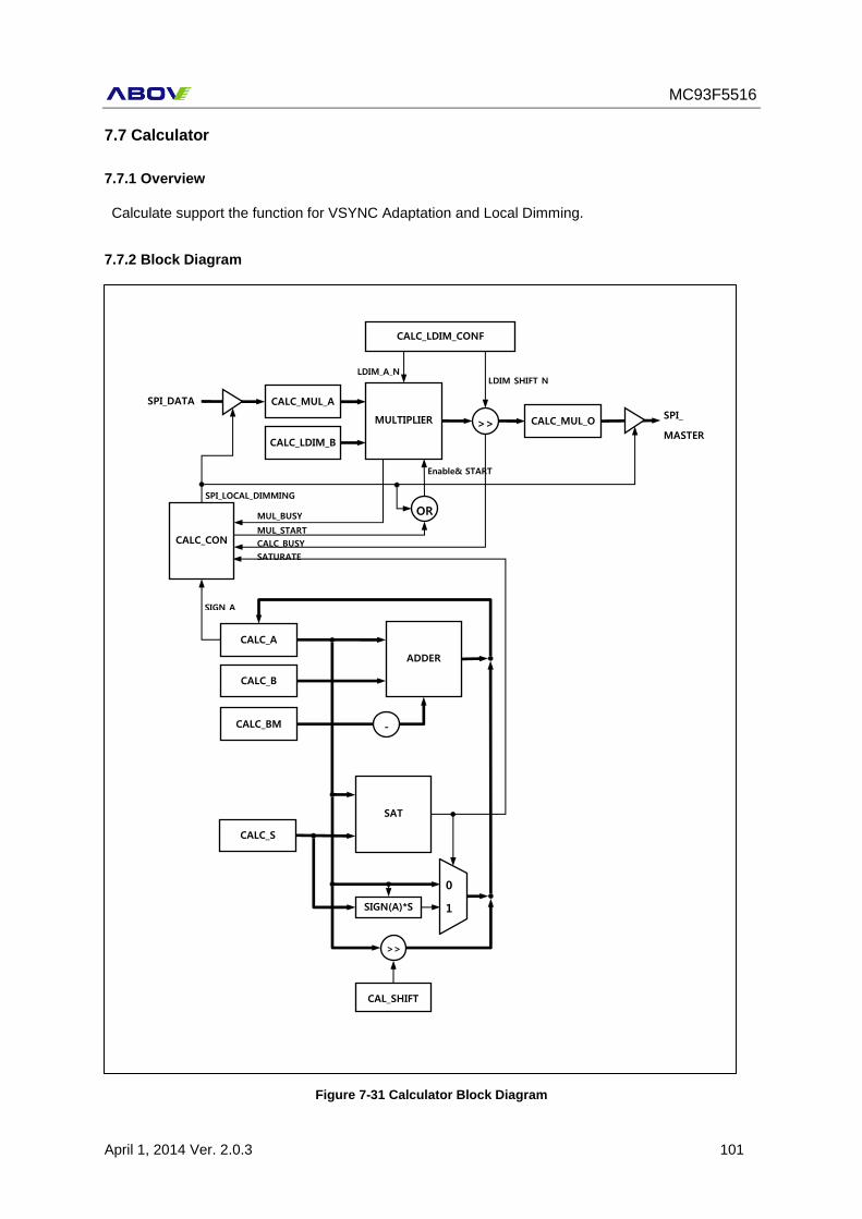
MC93F5516
April 1, 2014 Ver. 2.0.3 101
7.7 Calculator
7.7.1 Overview
Calculate support the function for VSYNC Adaptation and Local Dimming.
7.7.2 Block Diagram
Figure 7-31 Calculator Block Diagram
CALC_MUL_A
(16bit)
CALC_LDIM_B
(16bit)
MULTIPLIER CALC_MUL_O >>
CALC_A
CALC_B
ADDER
SAT
0
1
CALC_BM -
MUL_START
SATURATE
CALC_BUSY
SIGN_A
MUL_BUSY
SPI_DATA
SPI_
MASTER
>>
CAL_SHIFT
CALC_CON
SPI_LOCAL_DIMMING
SIGN(A)*S
CALC_LDIM_CONF
LDIM_A_N LDIM_SHIFT_N
OR
Enable& START
CALC_S
MC93F5516
102 April 1, 2014 Ver. 2.0.3
7.7.3 Function Description
Function Description Trigger
MUL
& Shifter
- ((CALC_MUL_A * CALC_LDIM_B)/ )/
CALC_MUL_O
- LDIM_A_N : the bit number of CALC_MUL_A
- LDIM_SHIFT_N : Additionally shift number
- Processing the data of SPI Array and sending to slave
though SPI Master.
Writing to CALC_MUL_A_L
ADD - CALC_A + CALC_B CALC_A Writing to CALC_B_L
SUB - CALC_A - CALC_BM CALC_A Writing to CALC_BM_L
Shifter - CALC_A >> CALC_SHIFT CALC_A Writing to CALC_SHIFT
SAT - SAT(A,B) = |A|>B ? SIGN(A)*B : A CALC_A Writing to CALC_S_L+NOP
7.7.3.1 The SFR Map of Calculator
Name Address Dir Default Description
CALC_CON C8H R/W 20H Calculator Control Register
CALC_SHIFT DFH R/W xxH Calculator Shift Register
CALC_A_L C9H R/W xxH Calculator A Register Low
CALC_A_M CAH R/W xxH Calculator A Register Middle
CALC_A_H CBH R/W xxH Calculator A Register High
CALC_B_L D1H R/W xxH Calculator B Register Low
CALC_B_M D2H R/W xxH Calculator BM Register Middle
CALC_B_H D3H R/W xxH Calculator BM Register High
CALC_BM_L D9H R/W xxH Calculator BM Register Low
CALC_BM_M DAH R/W xxH Calculator B Register Middle
CALC_BM_H DBH R/W xxH Calculator B Register High
CALC_S_L DCH R/W xxH Calculator SAT Register Low
CALC_S_M DDH R/W xxH Calculator SAT Register Middle
CALC_S_H DEH R/W xxH Calculator SAT Register High
CALC_MUL_A_L CCH R/W xxH Calculator MUL_A register Low
CALC_MUL_A_H CDH R/W xxH Calculator MUL_A register High
MC93F5516
April 1, 2014 Ver. 2.0.3 103
Name Address Dir Default Description
CALC_MUL_O_L CEH R/W xxH Calculator MUL_O register Low
CALC_MUL_O_H CFH R/W xxH Calculator MUL_O register High
CALC_LDIM_CONF 1027H R/W xxH Calculator Local DIMMING Configuration
CALC_LDIM_B_H 1028H R/W xxH Calculator Local Dimming B High
CALC_LDIM_B_L 1029H R/W xxH Calculator Local Dimming B Low
Table 7.9 Calculator Register Map
7.7.3.2 The SFR Description of Calculator
CALC_CON(Calculator Control Register) : C8H
7 6 5 4 3 2 1 0
MUL_BUSY CALC_BUSY - - SIGN_A SATURATE SPI_LOCAL_
DIMMING MUL_START
R R - - R R R/W R/W
Initial value: 20H
MUL_BUSY Multiplier & shifter status
0 Idle
1 Busy
CALC_BUSY Calculator status
0 Idle
1 Busy
SIGN_A Sign bit of A register
0 Positive
1 Negative
SATURATE |A| > B result @ SAT(A,B)
0 |A| ≤ B
1 |A| > B
SPI_LOCAL_DIMMING SPI Local Dimming enable bit
0 Diable
1 Enable: Mumtiplier & Shifter is connected to SPI local dimming data.
MUL_START MUL_START
0 Idle
1 Start Multiplier & shifter
MC93F5516
104 April 1, 2014 Ver. 2.0.3
CALC_SHIFT (Calculator Shift Register) : DFH
7 6 5 4 3 2 1 0
CALC_SHIFT7 CALC_SHIFT6 CALC_SHIFT5 CALC_SHIFT4 CALC_SHIFT3 CALC_SHIFT2 CALC_SHIFT1 CALC_SHIFT0
R/W R/W R/W R/W R/W R/W R/W R/W
Initial value: XXH
CALC_SHIFT[7:0] Calculator Shift Valure
The number of shift : CALC_SHIFT+1
If user want to shift 1, CALC_SHIFT value is 0.
CALC_A_L (Calculator A Low Register) : C9H
7 6 5 4 3 2 1 0
CALC_A7 CALC_A6 CALC_A5 CALC_A4 CALC_A3 CALC_A2 CALC_A1 CALC_A0
R/W R/W R/W R/W R/W R/W R/W R/W
Initial value: XXH
CALC_A[7:0] Calculator A Regiser Low Data
CALC_A_M (Calculator A Middle Register) : CAH
7 6 5 4 3 2 1 0
CALC_A15 CALC_A14 CALC_A13 CALC_A12 CALC_A11 CALC_A10 CALC_A9 CALC_A8
R/W R/W R/W R/W R/W R/W R/W R/W
Initial value: XXH
CALC_A[15:8] Calculator A Regiser Middle Data
CALC_A_H (Calculator A High Register) : CBH
7 6 5 4 3 2 1 0
CALC_A23 CALC_A22 CALC_A21 CALC_A20 CALC_A19 CALC_A18 CALC_A17 CALC_A16
R/W R/W R/W R/W R/W R/W R/W R/W
Initial value: XXH
CALC_A[23:16] Calculator A Regiser High Data
CALC_B_L (Calculator B Low Register) : D1H
7 6 5 4 3 2 1 0
CALC_B7 CALC_B6 CALC_B5 CALC_B4 CALC_B3 CALC_B2 CALC_B1 CALC_B0
R/W R/W R/W R/W R/W R/W R/W R/W
Initial value: XXH
CALC_B[7:0] Calculator B Regiser Low Data
CALC_B_M (Calculator B Middle Register) : D2H
7 6 5 4 3 2 1 0
CALC_B15 CALC_B14 CALC_B13 CALC_B12 CALC_B11 CALC_B10 CALC_B9 CALC_B8
R/W R/W R/W R/W R/W R/W R/W R/W
Initial value: XXH
CALC_B[15:8] Calculator B Regiser Middle Data
CALC_B_H (Calculator B High Register) : D3H
7 6 5 4 3 2 1 0
CALC_B23 CALC_B22 CALC_B21 CALC_B20 CALC_B19 CALC_B18 CALC_B17 CALC_B16
R/W R/W R/W R/W R/W R/W R/W R/W
Initial value: XXH
CALC_B[23:16] Calculator B Regiser High Data
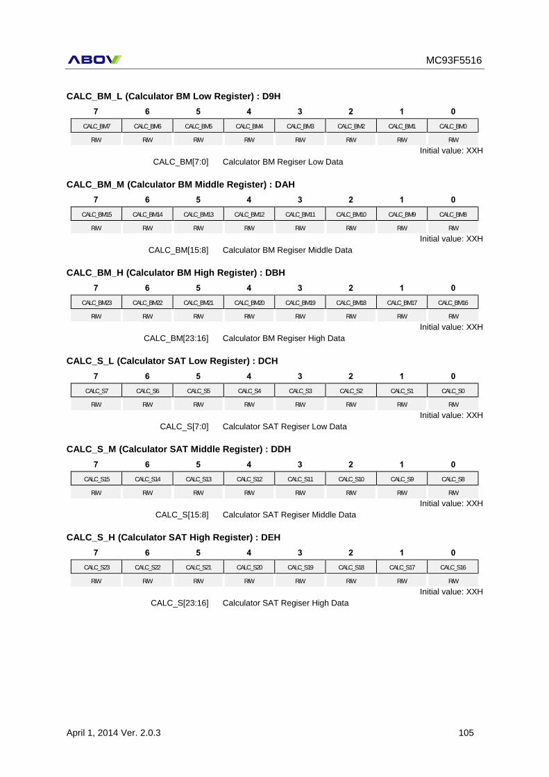
MC93F5516
April 1, 2014 Ver. 2.0.3 105
CALC_BM_L (Calculator BM Low Register) : D9H
7 6 5 4 3 2 1 0
CALC_BM7 CALC_BM6 CALC_BM5 CALC_BM4 CALC_BM3 CALC_BM2 CALC_BM1 CALC_BM0
R/W R/W R/W R/W R/W R/W R/W R/W
Initial value: XXH
CALC_BM[7:0] Calculator BM Regiser Low Data
CALC_BM_M (Calculator BM Middle Register) : DAH
7 6 5 4 3 2 1 0
CALC_BM15 CALC_BM14 CALC_BM13 CALC_BM12 CALC_BM11 CALC_BM10 CALC_BM9 CALC_BM8
R/W R/W R/W R/W R/W R/W R/W R/W
Initial value: XXH
CALC_BM[15:8] Calculator BM Regiser Middle Data
CALC_BM_H (Calculator BM High Register) : DBH
7 6 5 4 3 2 1 0
CALC_BM23 CALC_BM22 CALC_BM21 CALC_BM20 CALC_BM19 CALC_BM18 CALC_BM17 CALC_BM16
R/W R/W R/W R/W R/W R/W R/W R/W
Initial value: XXH
CALC_BM[23:16] Calculator BM Regiser High Data
CALC_S_L (Calculator SAT Low Register) : DCH
7 6 5 4 3 2 1 0
CALC_S7 CALC_S6 CALC_S5 CALC_S4 CALC_S3 CALC_S2 CALC_S1 CALC_S0
R/W R/W R/W R/W R/W R/W R/W R/W
Initial value: XXH
CALC_S[7:0] Calculator SAT Regiser Low Data
CALC_S_M (Calculator SAT Middle Register) : DDH
7 6 5 4 3 2 1 0
CALC_S15 CALC_S14 CALC_S13 CALC_S12 CALC_S11 CALC_S10 CALC_S9 CALC_S8
R/W R/W R/W R/W R/W R/W R/W R/W
Initial value: XXH
CALC_S[15:8] Calculator SAT Regiser Middle Data
CALC_S_H (Calculator SAT High Register) : DEH
7 6 5 4 3 2 1 0
CALC_S23 CALC_S22 CALC_S21 CALC_S20 CALC_S19 CALC_S18 CALC_S17 CALC_S16
R/W R/W R/W R/W R/W R/W R/W R/W
Initial value: XXH
CALC_S[23:16] Calculator SAT Regiser High Data
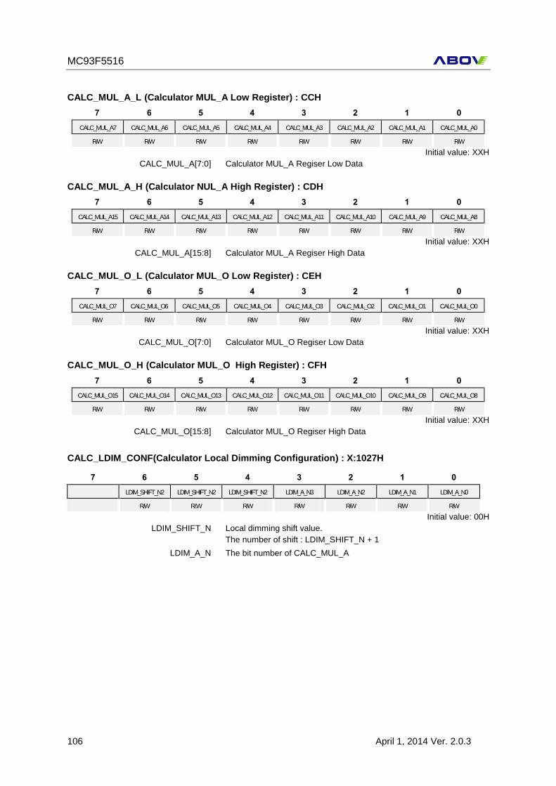
MC93F5516
106 April 1, 2014 Ver. 2.0.3
CALC_MUL_A_L (Calculator MUL_A Low Register) : CCH
7 6 5 4 3 2 1 0
CALC_MUL_A7 CALC_MUL_A6 CALC_MUL_A5 CALC_MUL_A4 CALC_MUL_A3 CALC_MUL_A2 CALC_MUL_A1 CALC_MUL_A0
R/W R/W R/W R/W R/W R/W R/W R/W
Initial value: XXH
CALC_MUL_A[7:0] Calculator MUL_A Regiser Low Data
CALC_MUL_A_H (Calculator NUL_A High Register) : CDH
7 6 5 4 3 2 1 0
CALC_MUL_A15 CALC_MUL_A14 CALC_MUL_A13 CALC_MUL_A12 CALC_MUL_A11 CALC_MUL_A10 CALC_MUL_A9 CALC_MUL_A8
R/W R/W R/W R/W R/W R/W R/W R/W
Initial value: XXH
CALC_MUL_A[15:8] Calculator MUL_A Regiser High Data
CALC_MUL_O_L (Calculator MUL_O Low Register) : CEH
7 6 5 4 3 2 1 0
CALC_MUL_O7 CALC_MUL_O6 CALC_MUL_O5 CALC_MUL_O4 CALC_MUL_O3 CALC_MUL_O2 CALC_MUL_O1 CALC_MUL_O0
R/W R/W R/W R/W R/W R/W R/W R/W
Initial value: XXH
CALC_MUL_O[7:0] Calculator MUL_O Regiser Low Data
CALC_MUL_O_H (Calculator MUL_O High Register) : CFH
7 6 5 4 3 2 1 0
CALC_MUL_O15 CALC_MUL_O14 CALC_MUL_O13 CALC_MUL_O12 CALC_MUL_O11 CALC_MUL_O10 CALC_MUL_O9 CALC_MUL_O8
R/W R/W R/W R/W R/W R/W R/W R/W
Initial value: XXH
CALC_MUL_O[15:8] Calculator MUL_O Regiser High Data
CALC_LDIM_CONF(Calculator Local Dimming Configuration) : X:1027H
7 6 5 4 3 2 1 0
LDIM_SHIFT_N2 LDIM_SHIFT_N2 LDIM_SHIFT_N2 LDIM_A_N3 LDIM_A_N2 LDIM_A_N1 LDIM_A_N0
R/W R/.W R/W R/W R/W R/W R/W
Initial value: 00H
LDIM_SHIFT_N Local dimming shift value.
The number of shift : LDIM_SHIFT_N + 1
LDIM_A_N The bit number of CALC_MUL_A
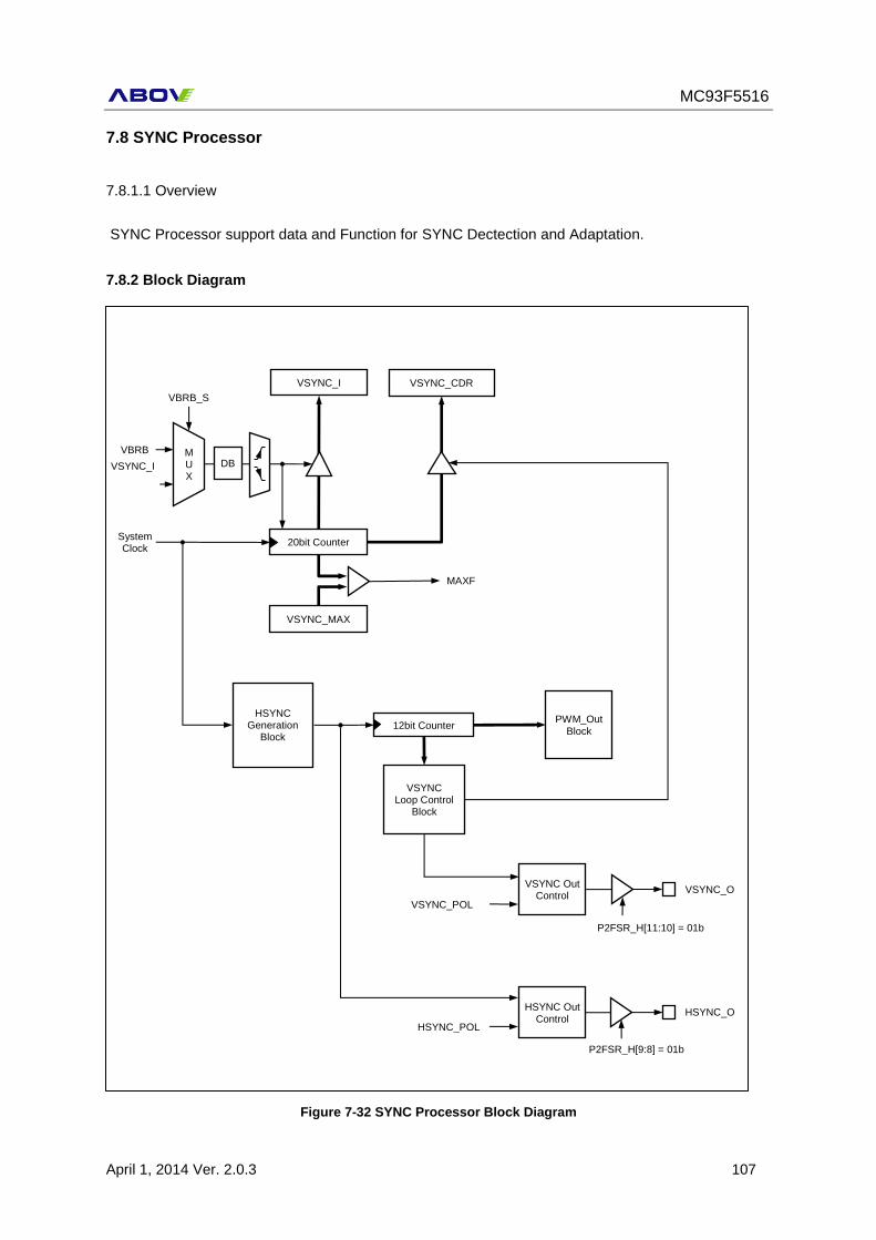
MC93F5516
April 1, 2014 Ver. 2.0.3 107
7.8 SYNC Processor
7.8.1.1 Overview
SYNC Processor support data and Function for SYNC Dectection and Adaptation.
7.8.2 Block Diagram
Figure 7-32 SYNC Processor Block Diagram
VSYNC_I
VSYNC_I
20bit Counter System Clock
VSYNC_CDR
VSYNC_MAX
MAXF
DB
VBRB M U X
VBRB_SEL
12bit Counter
VSYNC_O VSYNC Out
Control
P2FSR_H[11:10] = 01b
HSYNC_O
P2FSR_H[9:8] = 01b
PWM_Out Block
HSYNC Out Control
HSYNC_POL
VSYNC_POL
HSYNC Generation
Block
VSYNC Loop Control
Block
MC93F5516
108 April 1, 2014 Ver. 2.0.3
7.8.3 Function Description
Supported Data
- VSYNC_I : VSYNC Capture Data triggered by VSYNC_I input edge
- VSYNC_CDR : Capture Data from VSYNC_I to Internal VSYNC triggered by f_internal vsync_int of PWM Out Block
Function
- HSYNC Generation : HSYNC is generated by HSYNC_TR register value.
- VSYNC Out : Internal VSYNC ouput
- HSYNC Out : HSYNC generated output
- Multiplying & Dividing VSYNC
7.8.4 SFR MAP of the VSYNC Processor
Name Address Dir Default Description
SYNC_GEN_CON 98H R/W xxxx_xxx0B SYNC Generator Control Register
BLU_LED_CON F8H R/W xxxx_xxx0B LED BLU Control Register
VSYNC_I_L 99H R/W xxH VSYNC Capture Data Low Register
VSYNC_I_M 9AH R/W xxH VSYNC Capture Data Middle Register
VSYNC_I_H 9BH R/W xxH VSYNC Capture Data HIgh Register
VSYNC_CDR_L 9CH R/W xxH VSYNC Gap Capture Data Low Register
VSYNC_CDR_M 9DH R/W xxH VSYNC Gap Capture Data Middle Register
VSYNC_CDR_H 9EH R/W xxH VSYNC Gap Capture Data High Register
HSYNC_TR1_L F9H R/W xxH HSYNC TR1 Data Low Regiser
HSYNC_TR1_H FAH R/W xxH HSYNC TR1 Data High Regiser
HSYNC_TR2_L FBH R/W xxH HSYNC TR2 Data Low Regiser
HSYNC_TR2_H FCH R/W xxH HSYNC TR2 Data High Regiser
VSYNC_DB 100FH R/W xxH VSYNC Debounce Register
N_HSYNC_P_H 1020H R/W xxH HSYNC Number of Period High Regiser
N_HSYNC_P_L 1021H R/W xxH HSYNC Number of Period Low Regiser
N_HSYNC_P_LOOP 1022H R/W xxH N_HSYNC_P Loop Register
VSYNC_O_HIGH 1023H R/W xxH VSYNC Ouput High Period Data Register
VSYNC_MAX_H 1024H R/W xxH HSYNC MAX Data High Register
VSYNC_MAX_M 1025H R/W xxH HSYNC MAX Data Middle Register
VSYNC_MAX_L 1026H R/W xxH HSYNC MAX Data Low Register
N_VSYNC_INT_DLY 102CH R/W xxH Internal Vsync Delay Register
Table 7.10 VSYNG Processor SFR Map
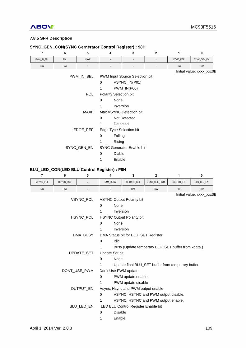
MC93F5516
April 1, 2014 Ver. 2.0.3 109
7.8.5 SFR Description
SYNC_GEN_CON(SYNC Gernerator Control Register) : 98H
7 6 5 4 3 2 1 0
PWM_IN_SEL POL MAXF - - - EDGE_REF SYNC_GEN_EN
R/W R/W R - - - R/W R/W
Initial value: xxxx_xxx0B
PWM_IN_SEL PWM Input Source Selection bit
0 VSYNC_IN(P01)
1 PWM_IN(P00)
POL Polarity Selection bit
0 None
1 Inversion
MAXF Max VSYNC Detection bit
0 Not Detected
1 Detected
EDGE_REF Edge Type Selection bit
0 Falling
1 Rising
SYNC_GEN_EN SYNC Generator Enable bit
0 Diable
1 Enable
BLU_LED_CON(LED BLU Control Register) : F8H
7 6 5 4 3 2 1 0
VSYNC_POL HSYNC_POL - DMA_BUSY UPDATE_SET DONT_USE_PWM OUTPUT_EN BLU_LED_EN
R/W R/W - R R/W R/W R R/W
Initial value: xxxx_xxx0B
VSYNC_POL VSYNC Output Polarity bit
0 None
1 Inversion
HSYNC_POL HSYNC Output Polarity bit
0 None
1 Inversion
DMA_BUSY DMA Status bit for BLU_SET Register
0 Idle
1 Busy (Update temperary BLU_SET buffer from xdata.)
UPDATE_SET Update Set bit
0 None
1 Update final BLU_SET buffer from temperary buffer
DONT_USE_PWM Don’t Use PWM update
0 PWM update enable
1 PWM update disable
OUTPUT_EN Vsync, Hsync and PWM output enable
0 VSYNC, HSYNC and PWM output disable.
1 VSYNC, HSYNC and PWM output enable.
BLU_LED_EN LED BLU Control Register Enable bit
0 Disable
1 Enable
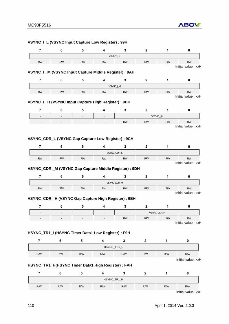
MC93F5516
110 April 1, 2014 Ver. 2.0.3
VSYNC_I_L (VSYNC Input Capture Low Register) : 99H
7 6 5 4 3 2 1 0
VSYNC_I_L
R/W R/W R/W R/W R/W R/W R/W R/W
Initial value : xxH
VSYNC_I _M (VSYNC Input Capture Middle Register) : 9AH
7 6 5 4 3 2 1 0
VSYNC_I_M
R/W R/W R/W R/W R/W R/W R/W R/W
Initial value : xxH
VSYNC_I _H (VSYNC Input Capture High Register) : 9BH
7 6 5 4 3 2 1 0
- - - - VSYNC_I_H
- - - - R/W R/W R/W R/W
Initial value : xxH
VSYNC_CDR_L (VSYNC Gap Capture Low Register) : 9CH
7 6 5 4 3 2 1 0
VSYNC_CDR_L
R/W R/W R/W R/W R/W R/W R/W R/W
Initial value : xxH
VSYNC_CDR _M (VSYNC Gap Capture Middle Register) : 9DH
7 6 5 4 3 2 1 0
VSYNC_CDR_M
R/W R/W R/W R/W R/W R/W R/W R/W
Initial value : xxH
VSYNC_CDR _H (VSYNC Gap Capture High Register) : 9EH
7 6 5 4 3 2 1 0
- - - - VSYNC_CDR_H
- - - - R/W R/W R/W R/W
Initial value : xxH
HSYNC_TR1_L(HSYNC Timer Data1 Low Register) : F9H
7 6 5 4 3 2 1 0
HSYNC_TR1_L
R/W R/W R/W R/W R/W R/W R/W R/W
Initial value: xxH
HSYNC_TR1_H(HSYNC Timer Data1 High Register) : FAH
7 6 5 4 3 2 1 0
HSYNC_TR1_H
R/W R/W R/W R/W R/W R/W R/W R/W
Initial value: xxH
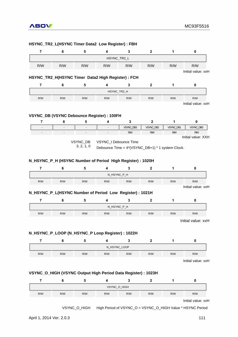
MC93F5516
April 1, 2014 Ver. 2.0.3 111
HSYNC_TR2_L(HSYNC Timer Data2 Low Register) : FBH
7 6 5 4 3 2 1 0
HSYNC_TR2_L
R/W R/W R/W R/W R/W R/W R/W R/W
Initial value: xxH
HSYNC_TR2_H(HSYNC Timer Data2 High Register) : FCH
7 6 5 4 3 2 1 0
HSYNC_TR2_H
R/W R/W R/W R/W R/W R/W R/W R/W
Initial value: xxH
VSYNC_DB (VSYNC Debounce Register) : 100FH
7 6 5 4 3 2 1 0
- - - - VSYNC_DB3 VSYNC_DB2 VSYNC_DB1 VSYNC_DB0
- - - - R/W R/W R/W R/W
Initial value: XXH
VSYNC_DB 3, 2, 1, 0
VSYNC_I Debounce Time
Debounce Time = 4*(VSYNC_DB+1) * 1 system Clock.
N_HSYNC_P_H (HSYNC Number of Period High Register) : 1020H
7 6 5 4 3 2 1 0
N_HSYNC_P_H
R/W R/W R/W R/W R/W R/W R/W R/W
Initial value: xxH
N_HSYNC_P_L(HSYNC Number of Period Low Register) : 1021H
7 6 5 4 3 2 1 0
N_HSYNC_P_H
R/W R/W R/W R/W R/W R/W R/W R/W
Initial value: xxH
N_HSYNC_P_LOOP (N_HSYNC_P Loop Register) : 1022H
7 6 5 4 3 2 1 0
N_HSYNC_LOOP
R/W R/W R/W R/W R/W R/W R/W R/W
Initial value: xxH
VSYNC_O_HIGH (VSYNC Output High Period Data Register) : 1023H
7 6 5 4 3 2 1 0
VSYNC_O_HIGH
R/W R/W R/W R/W R/W R/W R/W R/W
Initial value: xxH
VSYNC_O_HIGH High Period of VSYNC_O = VSYNC_O_HIGH Value * HSYNC Period
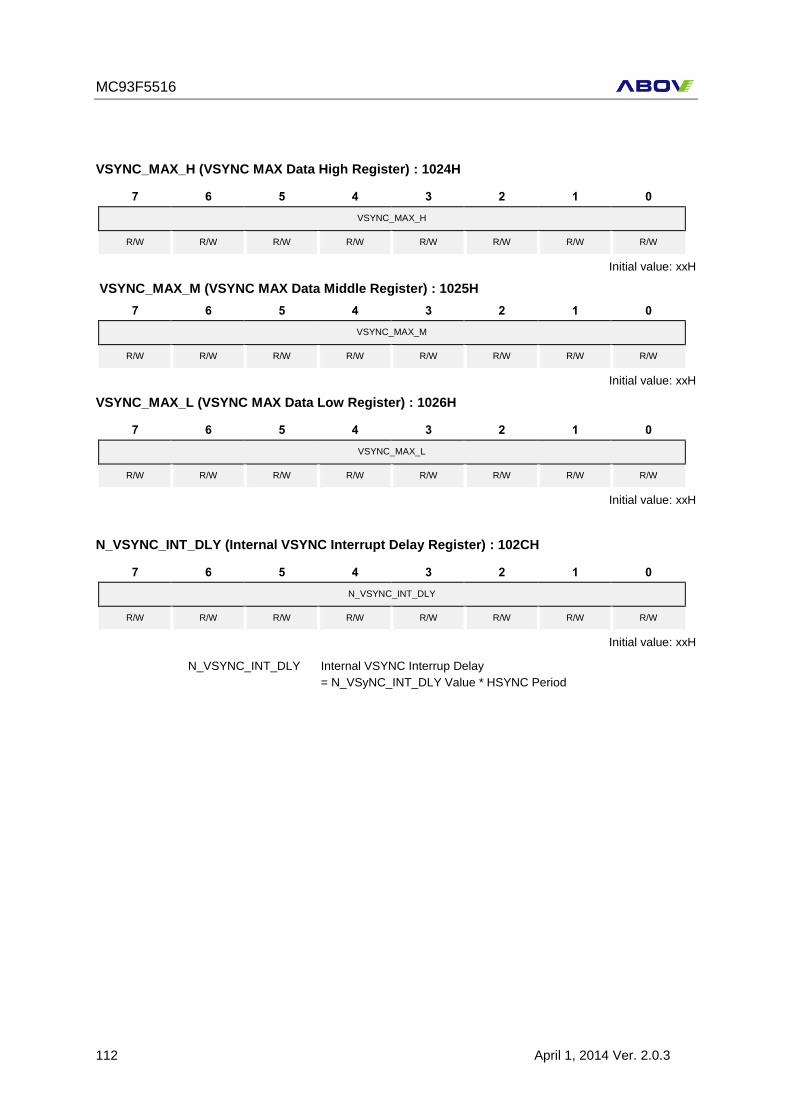
MC93F5516
112 April 1, 2014 Ver. 2.0.3
VSYNC_MAX_H (VSYNC MAX Data High Register) : 1024H
7 6 5 4 3 2 1 0
VSYNC_MAX_H
R/W R/W R/W R/W R/W R/W R/W R/W
Initial value: xxH
VSYNC_MAX_M (VSYNC MAX Data Middle Register) : 1025H
7 6 5 4 3 2 1 0
VSYNC_MAX_M
R/W R/W R/W R/W R/W R/W R/W R/W
Initial value: xxH
VSYNC_MAX_L (VSYNC MAX Data Low Register) : 1026H
7 6 5 4 3 2 1 0
VSYNC_MAX_L
R/W R/W R/W R/W R/W R/W R/W R/W
Initial value: xxH
N_VSYNC_INT_DLY (Internal VSYNC Interrupt Delay Register) : 102CH
7 6 5 4 3 2 1 0
N_VSYNC_INT_DLY
R/W R/W R/W R/W R/W R/W R/W R/W
Initial value: xxH
N_VSYNC_INT_DLY Internal VSYNC Interrup Delay
= N_VSyNC_INT_DLY Value * HSYNC Period
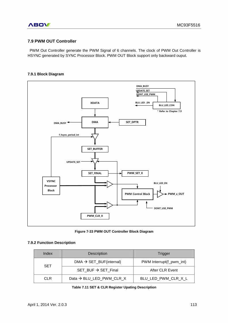
MC93F5516
April 1, 2014 Ver. 2.0.3 113
7.9 PWM OUT Controller
PWM Out Controller generate the PWM Signal of 6 channels. The clock of PWM Out Controller is
HSYNC generated by SYNC Processor Block. PWM OUT Block support only backward ouput.
7.9.1 Block Diagram
Figure 7-33 PWM OUT Controller Block Diagram
7.9.2 Function Description
Index Description Trigger
SET DMA SET_BUF(internal) PWM Interrupt(f_pwm_int)
SET_BUF SET_Final After CLR Event
CLR Data BLU_LED_PWM_CLR_X BLU_LED_PWM_CLR_X_L
Table 7.11 SET & CLR Register Upating Description
PWM_CLR_X
SET_FINAL
PWM_x_OUT PWM Control Block
XDATA
SET_DPTR DMA
PWM_SET_X
SET_BUFFER
f_hsync_period_int
BLU_LED_EN
DMA_BUSY
UPDATE_SET
VSYNC
Processor
Block
BLU_LED_CON BLU_LED _EN
DMA_BUSY
UPDATE_SET DONT_USE_PWM
DONT_USE_PWM
* Refer to Chapter 7.9

MC93F5516
114 April 1, 2014 Ver. 2.0.3
7.9.3 SFR MAP of the LED Controller
Name Address Dir Default Description
BLU_DPTR_SET_H 102A R/W xxH BLU Data Pointer High Register
BLU_DPTR_SET_L 102B R/W xxH BLU Data Pointer Low Register
PWM_SET_0_H 1030H R xxH PWM0 SET Data Register
PWM_SET_0_L 1031H R xxH
PWM_SET_1_H 1032H R xxH PWM1 SET Data Register
PWM_SET_1_L 1033H R xxH
PWM_SET_2_H 1034H R xxH PWM2 SET Data Register
PWM_SET_2_L 1035H R xxH
PWM_SET_3_H 1036H R xxH PWM3 SET Data Register
PWM_SET_3_L 1037H R xxH
PWM_SET_4_H 1038H R xxH PWM4 SET Data Register
PWM_SET_4_L 1039H R xxH
PWM_SET_5_H 103AH R xxH PWM5 SET Data Register
PWM_SET_5_L 103BH R xxH
PWM_CLR_0_H 1040H R/W xxH PWM0 CLR Data Register
PWM_CLR_0_L 1041H R/W xxH
PWM_CLR _1_H 1042H R/W xxH PWM1 CLR Data Register
PWM_CLR _1_L 1043H R/W xxH
PWM_CLR _2_H 1044H R/W xxH PWM2 CLR Data Register
PWM_CLR _2_L 1045H R/W xxH
PWM_CLR _3_H 1046H R/W xxH PWM3 CLR Data Register
PWM_CLR_3_L 1047H R/W xxH
PWM_CLR_4_H 1048H R/W xxH PWM4 CLR Data Register
PWM_CLR_4_L 1049H R/W xxH
PWM_CLR_5_H 104AH R/W xxH PWM5 CLR Data Register
PWM_CLR_5_L 104BH R/W xxH
Table 7.12 SFR Map of the PWM Out Controller
MC93F5516
April 1, 2014 Ver. 2.0.3 115
7.9.3.1 The SFR Description of LED Driver Controller
BLU_DPTR_SET_H (BLU Data Point MSB) : 102AH
7 6 5 4 3 2 1 0
BLU_DPTR_SET_H
R/W R/W R/W R/W R/W R/W R/W R/W
Initial value: xxH
BLU_DPTR_SET_L (BLU Data Point LSB) : 102BH
7 6 5 4 3 2 1 0
BLU_DPTR_SET_L
R/W R/W R/W R/W R/W R/W R/W R/W
Initial value: xxH
PWM_SET_X_H (PWMx SET Data High Register, X : 0~5) : 1030/1032/1034/1036/1038/103AH
7 6 5 4 3 2 1 0
PWM_SET_x_H
R R R R R R R R
Initial value: xxH
PWM_SET_X_L (PWMx SET Data Low Register, X : 0~5) : 1031/1033/1035/1037/1039/103BH
7 6 5 4 3 2 1 0
PWM_SET_x_L
R R R R R R R R
Initial value: xxH
PWM_CLR_X_H (PWMx CLR Data High Register, X : 0~5) : 1040/1042/1044/1046/1048/104AH
7 6 5 4 3 2 1 0
PWM_CLR_x_H
R/W R/W R/W R/W R/W R/W R/W R/W
Initial value: xxH
PWM_CLR_X_L (PWMx CLR Data Low Register, X : 0~5) : 1041/1043/1045/1047/1049/104BH
7 6 5 4 3 2 1 0
PWM_CLR_x_L
R/W R/W R/W R/W R/W R/W R/W R/W
Initial value: xxH
MC93F5516
116 April 1, 2014 Ver. 2.0.3
8. Memory Programming
8.1 Overview
8.1.1 Description
MC93F5516 incorporates flash memory to which a program can be written, erased, and overwritten
while mounted on the board. Flash area can be programmed in OCD or parallel ROM mode. And This
device support the self program/erase mode in user soft mode.
Serial ISP mode is supported.
8.1.2 Features
• Flash Size : 16Kbytes
• Single power supply program and erase
• Command interface for fast program and erase operation
• Up to 1,000 program/erase cycles at typical voltage and temperature for flash memory
• Security feature
8.2 Flash and EEPROM Control and status register
Registers to control Flash and Data EEPROM are Mode Register (FEMR), Control Register (FECR),
Status Register (FESR), Time Control Register (FETCR), Address Low Register (FEARL), Address
Middle Register (FEARM), address High Register (FEARH) and Data Register (FEDR). They are
mapped to SFR area and can be accessed only in programming mode.
8.2.1 Register Map
Table 8.1 Register Map
Name Address Dir Default Description
FEMR EAH R/W 00H Flash and EEPROM Mode Register
FECR EBH R/W 03H Flash and EEPROM Control Register
FESR ECH R/W 80H Flash and EEPROM Status Register
FETCR EDH R/W 00H Flash and EEPROM Time Control Register
FEARL F2H R/W 00H Flash and EEPROM Address Low Register
FEARM F3H R/W 00H Flash and EEPROM Address Middle Register
FEARH F4H R/W 00H Flash and EEPROM Address High Register
FEDR F5H R/W 00H Flash and EEPROM Data Register
MC93F5516
April 1, 2014 Ver. 2.0.3 117
8.2.2 Register description for Flash and EEPROM
FEMR (Flash and EEPROM Mode Register) : EAH
7 6 5 4 3 2 1 0
FSEL ESEL PGM ERASE PBUFF OTPE VFY FEEN
R/W R/W R/W R/W R/W R/W R/W R/W
Initial value : 00H
FSEL Select flash memory.
0 Deselect flash memory
1 Select flash memory
ESEL Select data EEPROM
0 Deselect data EEPROM
1 Select data EEPROM
PGM Enable program or program verify mode with VFY
0 Disable program or program verify mode
1 Enable program or program verify mode
ERASE Enable erase or erase verify mode with VFY
0 Disable erase or erase verify mode
1 Enable erase or erase verify mode
PBUFF Select page buffer
0 Deselect page buffer
1 Select page buffer
OTPE Select OTP area instead of program memory
0 Deselect OTP area
1 Select OTP area
VFY Set program or erase verify mode with PGM or ERASE
Program Verify: PGM=1, VFY=1
Erase Verify: ERASE=1, VFY=1
FEEN Enable program and erase of Flash and data EEPROM. When inactive, it is possible to read as normal mode
0 Disable program and erase
1 Enable program and erase
FECR (Flash and EEPROM Control Register) : EBH
7 6 5 4 3 2 1 0
AEF AEE EXIT1 EXIT0 WRITE READ nFERST nPBRST
R/W R/W R/W R/W R/W R/W R/W R/W
Initial value : 03H
AEF Enable flash bulk erase mode
0 Disable bulk erase mode of Flash memory
1 Enable bulk erase mode of Flash memory
AEE Enable data EEPROM bulk erase mode
0 Disable bulk erase mode of data EEPROM
1 Enable bulk erase mode of data EEPROM
EXIT[1:0] Exit from program mode. It is cleared automatically after 1 clock
EXIT1 EXIT0 Description
0 0 Don’t exit from program mode
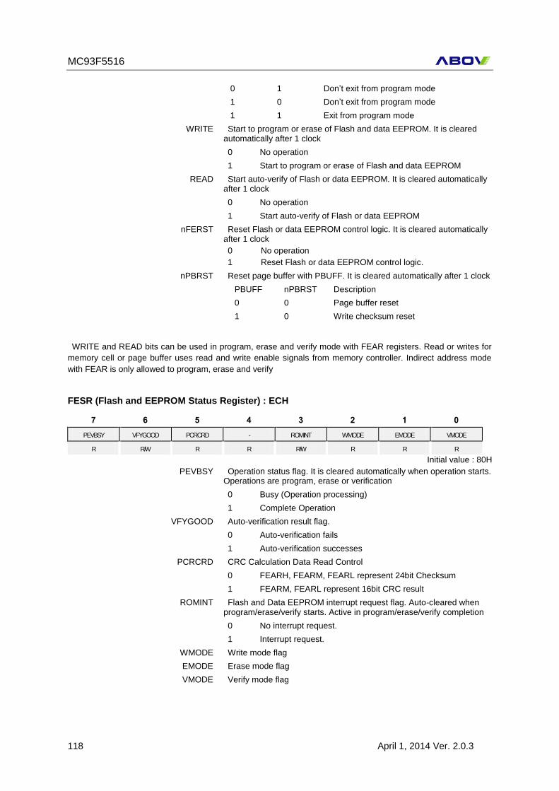
MC93F5516
118 April 1, 2014 Ver. 2.0.3
0 1 Don’t exit from program mode
1 0 Don’t exit from program mode
1 1 Exit from program mode
WRITE Start to program or erase of Flash and data EEPROM. It is cleared automatically after 1 clock
0 No operation
1 Start to program or erase of Flash and data EEPROM
READ Start auto-verify of Flash or data EEPROM. It is cleared automatically after 1 clock
0 No operation
1 Start auto-verify of Flash or data EEPROM
nFERST Reset Flash or data EEPROM control logic. It is cleared automatically after 1 clock
0 No operation
1 Reset Flash or data EEPROM control logic.
nPBRST Reset page buffer with PBUFF. It is cleared automatically after 1 clock
PBUFF nPBRST Description
0 0 Page buffer reset
1 0 Write checksum reset
WRITE and READ bits can be used in program, erase and verify mode with FEAR registers. Read or writes for
memory cell or page buffer uses read and write enable signals from memory controller. Indirect address mode
with FEAR is only allowed to program, erase and verify
FESR (Flash and EEPROM Status Register) : ECH
7 6 5 4 3 2 1 0
PEVBSY VFYGOOD PCRCRD - ROMINT WMODE EMODE VMODE
R R/W R R R/W R R R
Initial value : 80H
PEVBSY Operation status flag. It is cleared automatically when operation starts. Operations are program, erase or verification
0 Busy (Operation processing)
1 Complete Operation
VFYGOOD Auto-verification result flag.
0 Auto-verification fails
1 Auto-verification successes
PCRCRD CRC Calculation Data Read Control
0 FEARH, FEARM, FEARL represent 24bit Checksum
1 FEARM, FEARL represent 16bit CRC result
ROMINT Flash and Data EEPROM interrupt request flag. Auto-cleared when program/erase/verify starts. Active in program/erase/verify completion
0 No interrupt request.
1 Interrupt request.
WMODE Write mode flag
EMODE Erase mode flag
VMODE Verify mode flag
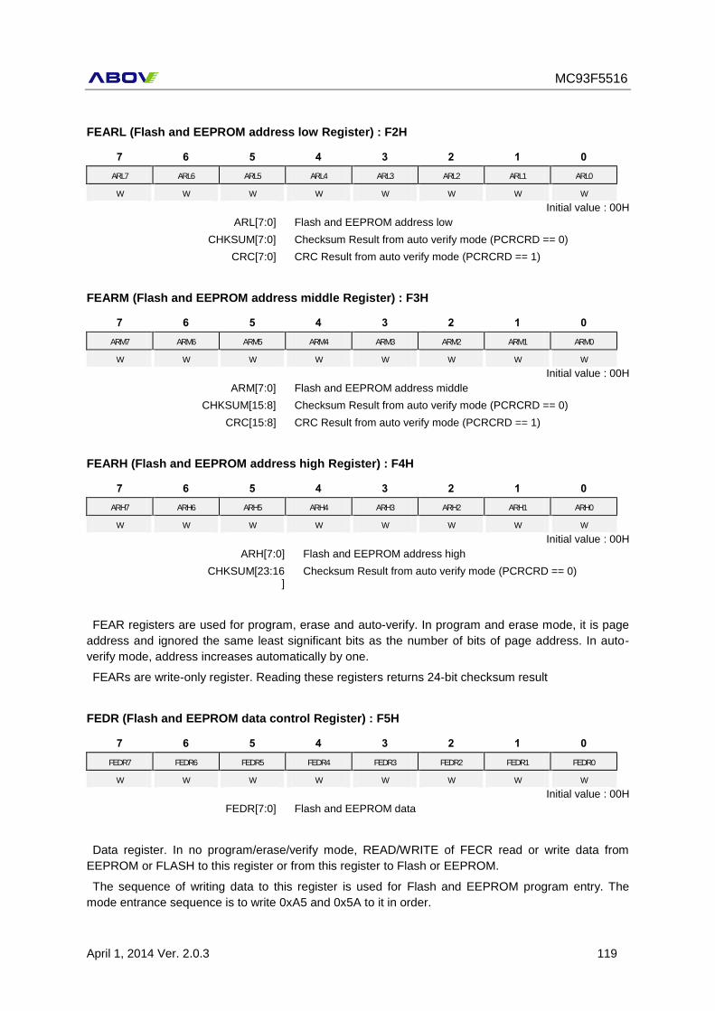
MC93F5516
April 1, 2014 Ver. 2.0.3 119
FEARL (Flash and EEPROM address low Register) : F2H
7 6 5 4 3 2 1 0
ARL7 ARL6 ARL5 ARL4 ARL3 ARL2 ARL1 ARL0
W W W W W W W W
Initial value : 00H
ARL[7:0] Flash and EEPROM address low
CHKSUM[7:0] Checksum Result from auto verify mode (PCRCRD == 0)
CRC[7:0] CRC Result from auto verify mode (PCRCRD == 1)
FEARM (Flash and EEPROM address middle Register) : F3H
7 6 5 4 3 2 1 0
ARM7 ARM6 ARM5 ARM4 ARM3 ARM2 ARM1 ARM0
W W W W W W W W
Initial value : 00H
ARM[7:0] Flash and EEPROM address middle
CHKSUM[15:8] Checksum Result from auto verify mode (PCRCRD == 0)
CRC[15:8] CRC Result from auto verify mode (PCRCRD == 1)
FEARH (Flash and EEPROM address high Register) : F4H
7 6 5 4 3 2 1 0
ARH7 ARH6 ARH5 ARH4 ARH3 ARH2 ARH1 ARH0
W W W W W W W W
Initial value : 00H
ARH[7:0] Flash and EEPROM address high
CHKSUM[23:16]
Checksum Result from auto verify mode (PCRCRD == 0)
FEAR registers are used for program, erase and auto-verify. In program and erase mode, it is page
address and ignored the same least significant bits as the number of bits of page address. In auto-
verify mode, address increases automatically by one.
FEARs are write-only register. Reading these registers returns 24-bit checksum result
FEDR (Flash and EEPROM data control Register) : F5H
7 6 5 4 3 2 1 0
FEDR7 FEDR6 FEDR5 FEDR4 FEDR3 FEDR2 FEDR1 FEDR0
W W W W W W W W
Initial value : 00H
FEDR[7:0] Flash and EEPROM data
Data register. In no program/erase/verify mode, READ/WRITE of FECR read or write data from
EEPROM or FLASH to this register or from this register to Flash or EEPROM.
The sequence of writing data to this register is used for Flash and EEPROM program entry. The
mode entrance sequence is to write 0xA5 and 0x5A to it in order.
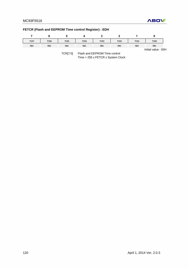
MC93F5516
120 April 1, 2014 Ver. 2.0.3
FETCR (Flash and EEPROM Time control Register) : EDH
7 6 5 4 3 2 1 0
TCR7 TCR6 TCR5 TCR4 TCR3 TCR2 TCR1 TCR0
R/W R/W R/W R/W R/W R/W R/W R/W
Initial value : 00H
TCR[7:0] Flash and EEPROM Time control
Time = 255 x FETCR x System Clock
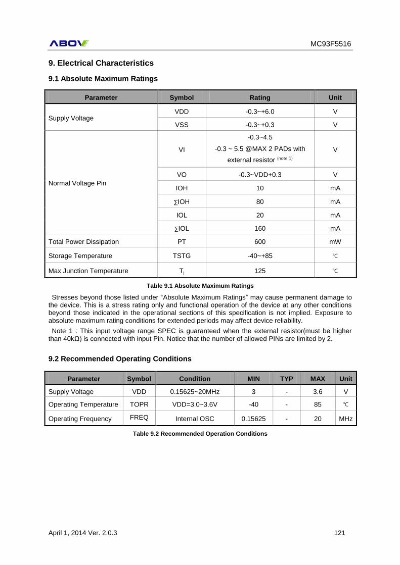
MC93F5516
April 1, 2014 Ver. 2.0.3 121
9. Electrical Characteristics
9.1 Absolute Maximum Ratings
Parameter Symbol Rating Unit
Supply Voltage VDD -0.3~+6.0 V
VSS -0.3~+0.3 V
Normal Voltage Pin
VI
-0.3~4.5
-0.3 ~ 5.5 @MAX 2 PADs with
external resistor (note 1)
V
VO -0.3~VDD+0.3 V
IOH 10 mA
∑IOH 80 mA
IOL 20 mA
∑IOL 160 mA
Total Power Dissipation PT 600 mW
Storage Temperature TSTG -40~+85
Max Junction Temperature Tj 125
Table 9.1 Absolute Maximum Ratings
Stresses beyond those listed under “Absolute Maximum Ratings” may cause permanent damage to the device. This is a stress rating only and functional operation of the device at any other conditions beyond those indicated in the operational sections of this specification is not implied. Exposure to absolute maximum rating conditions for extended periods may affect device reliability.
Note 1 : This input voltage range SPEC is guaranteed when the external resistor(must be higher than 40kΩ) is connected with input Pin. Notice that the number of allowed PINs are limited by 2.
9.2 Recommended Operating Conditions
Parameter Symbol Condition MIN TYP MAX Unit
Supply Voltage VDD 0.15625~20MHz 3 - 3.6 V
Operating Temperature TOPR VDD=3.0~3.6V -40 - 85
Operating Frequency FREQ Internal OSC 0.15625 - 20 MHz
Table 9.2 Recommended Operation Conditions
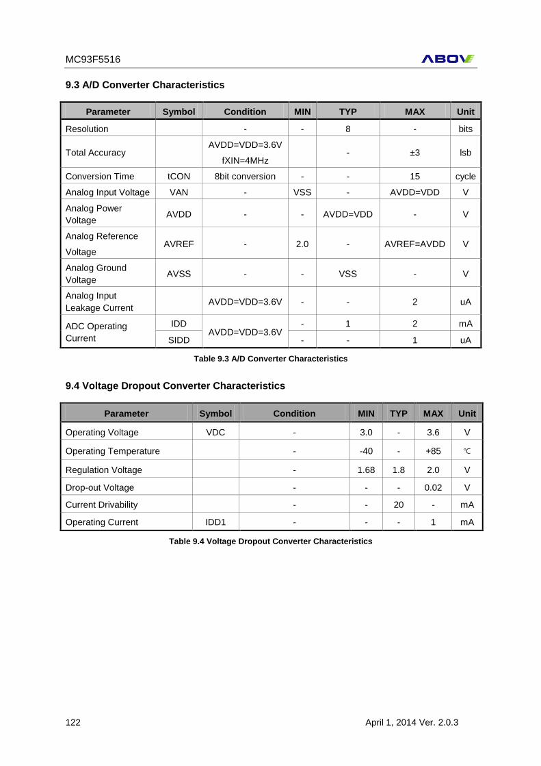
MC93F5516
122 April 1, 2014 Ver. 2.0.3
9.3 A/D Converter Characteristics
Parameter Symbol Condition MIN TYP MAX Unit
Resolution - - 8 - bits
Total Accuracy AVDD=VDD=3.6V
fXIN=4MHz - ±3 lsb
Conversion Time tCON 8bit conversion - - 15 cycle
Analog Input Voltage VAN - VSS - AVDD=VDD V
Analog Power
Voltage AVDD - - AVDD=VDD - V
Analog Reference
Voltage AVREF - 2.0 - AVREF=AVDD V
Analog Ground
Voltage AVSS - - VSS - V
Analog Input
Leakage Current AVDD=VDD=3.6V - - 2 uA
ADC Operating
Current
IDD AVDD=VDD=3.6V
- 1 2 mA
SIDD - - 1 uA
Table 9.3 A/D Converter Characteristics
9.4 Voltage Dropout Converter Characteristics
Parameter Symbol Condition MIN TYP MAX Unit
Operating Voltage VDC - 3.0 - 3.6 V
Operating Temperature - -40 - +85
Regulation Voltage - 1.68 1.8 2.0 V
Drop-out Voltage - - - 0.02 V
Current Drivability - - 20 - mA
Operating Current IDD1 - - - 1 mA
Table 9.4 Voltage Dropout Converter Characteristics
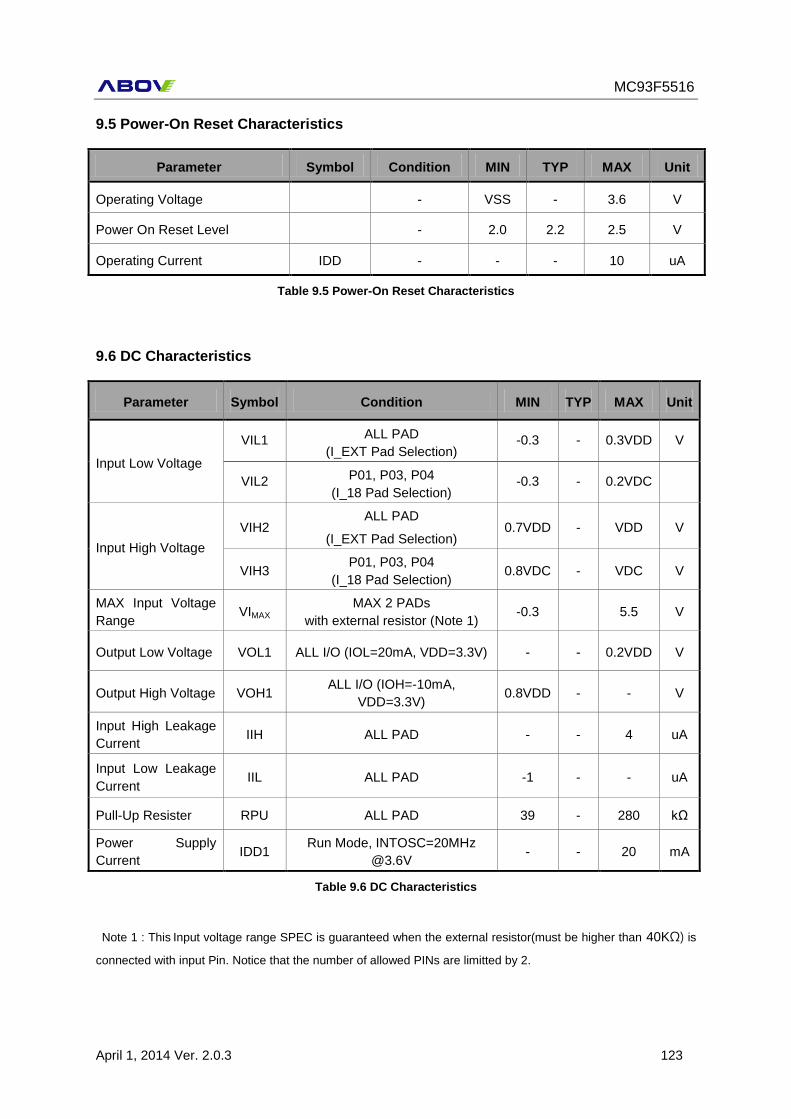
MC93F5516
April 1, 2014 Ver. 2.0.3 123
9.5 Power-On Reset Characteristics
Parameter Symbol Condition MIN TYP MAX Unit
Operating Voltage - VSS - 3.6 V
Power On Reset Level - 2.0 2.2 2.5 V
Operating Current IDD - - - 10 uA
Table 9.5 Power-On Reset Characteristics
9.6 DC Characteristics
Parameter Symbol Condition MIN TYP MAX Unit
Input Low Voltage
VIL1 ALL PAD
(I_EXT Pad Selection) -0.3 - 0.3VDD V
VIL2 P01, P03, P04
(I_18 Pad Selection) -0.3 - 0.2VDC
Input High Voltage
VIH2 ALL PAD
(I_EXT Pad Selection) 0.7VDD - VDD V
VIH3 P01, P03, P04
(I_18 Pad Selection) 0.8VDC - VDC V
MAX Input Voltage
Range VIMAX
MAX 2 PADs
with external resistor (Note 1) -0.3 5.5 V
Output Low Voltage VOL1 ALL I/O (IOL=20mA, VDD=3.3V) - - 0.2VDD V
Output High Voltage VOH1 ALL I/O (IOH=-10mA,
VDD=3.3V) 0.8VDD - - V
Input High Leakage
Current IIH ALL PAD - - 4 uA
Input Low Leakage
Current IIL ALL PAD -1 - - uA
Pull-Up Resister RPU ALL PAD 39 - 280 kΩ
Power Supply
Current IDD1
Run Mode, INTOSC=20MHz
@3.6V - - 20 mA
Table 9.6 DC Characteristics
Note 1 : This Input voltage range SPEC is guaranteed when the external resistor(must be higher than 40KΩ) is
connected with input Pin. Notice that the number of allowed PINs are limitted by 2.
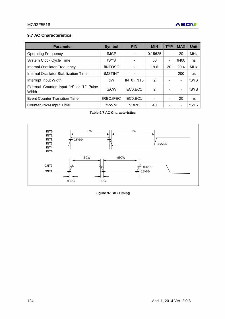
MC93F5516
124 April 1, 2014 Ver. 2.0.3
9.7 AC Characteristics
Parameter Symbol PIN MIN TYP MAX Unit
Operating Frequency fMCP - 0.15625 - 20 MHz
System Clock Cycle Time tSYS - 50 - 6400 ns
Internal Oscillator Frequency fINTOSC - 19.6 20 20.4 MHz
Internal Oscillator Stabilization Time tMSTINT - 200 us
Interrupt Input Width tIW INT0~INT5 2 - - tSYS
External Counter Input “H” or “L” Pulse
Width tECW EC0,EC1 2 - - tSYS
Event Counter Transition Time tREC,tFEC EC0,EC1 - - 20 ns
Counter PWM Input Time tPWM VBRB 40 - - tSYS
Table 9.7 AC Characteristics
CNT0
0.8VDD
0.2VDD
tIW tIW
0.8VDD
0.2VDD
tECW tECW
INT0
INT1
INT2
INT3
INT4
INT5
tREC tFEC
CNT1
Figure 9-1 AC Timing
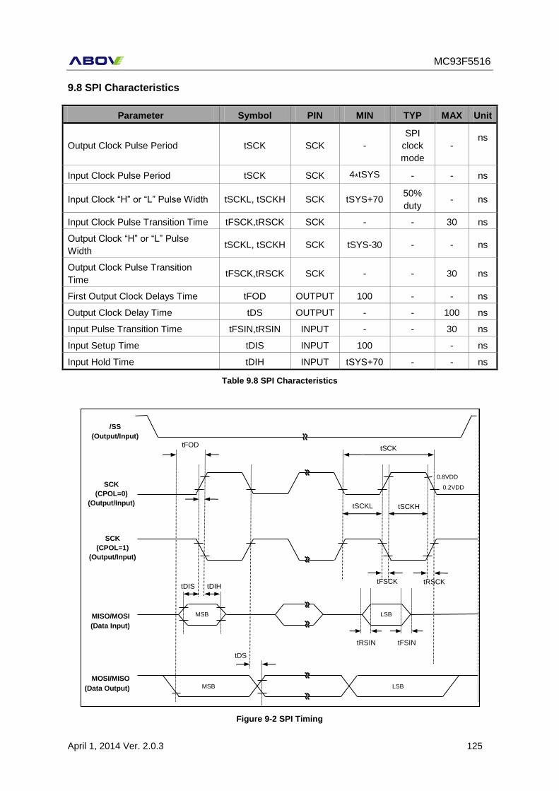
MC93F5516
April 1, 2014 Ver. 2.0.3 125
9.8 SPI Characteristics
Parameter Symbol PIN MIN TYP MAX Unit
Output Clock Pulse Period tSCK SCK -
SPI
clock
mode
- ns
Input Clock Pulse Period tSCK SCK 4*tSYS - - ns
Input Clock “H” or “L” Pulse Width tSCKL, tSCKH SCK tSYS+70 50%
duty - ns
Input Clock Pulse Transition Time tFSCK,tRSCK SCK - - 30 ns
Output Clock “H” or “L” Pulse
Width tSCKL, tSCKH SCK tSYS-30 - - ns
Output Clock Pulse Transition
Time tFSCK,tRSCK SCK - - 30 ns
First Output Clock Delays Time tFOD OUTPUT 100 - - ns
Output Clock Delay Time tDS OUTPUT - - 100 ns
Input Pulse Transition Time tFSIN,tRSIN INPUT - - 30 ns
Input Setup Time tDIS INPUT 100 - ns
Input Hold Time tDIH INPUT tSYS+70 - - ns
Table 9.8 SPI Characteristics
SCK
(CPOL=1)
(Output/Input)
MOSI/MISO
(Data Output)
MISO/MOSI
(Data Input)
tSCK
tRSIN
0.8VDD
0.2VDD
tDS
SCK
(CPOL=0)
(Output/Input)
tSCKH tSCKL
/SS
(Output/Input)
MSB LSB
LSB MSB
tDIS tDIH tFSCK tRSCK
tFSIN
tFOD
Figure 9-2 SPI Timing
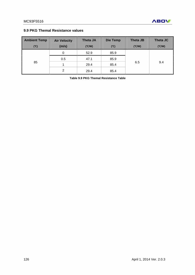
MC93F5516
126 April 1, 2014 Ver. 2.0.3
9.9 PKG Themal Resistance values
Ambient Temp
()
Air Velocity
(m/s)
Theta JA
(/W)
Die Temp
()
Theta JB
(/W)
Theta JC
(/W)
85
0 52.9 85.9
6.5 9.4 0.5 47.1 85.9
1 29.4 85.4
2 29.4 85.4
Table 9.9 PKG Themal Resistance Table
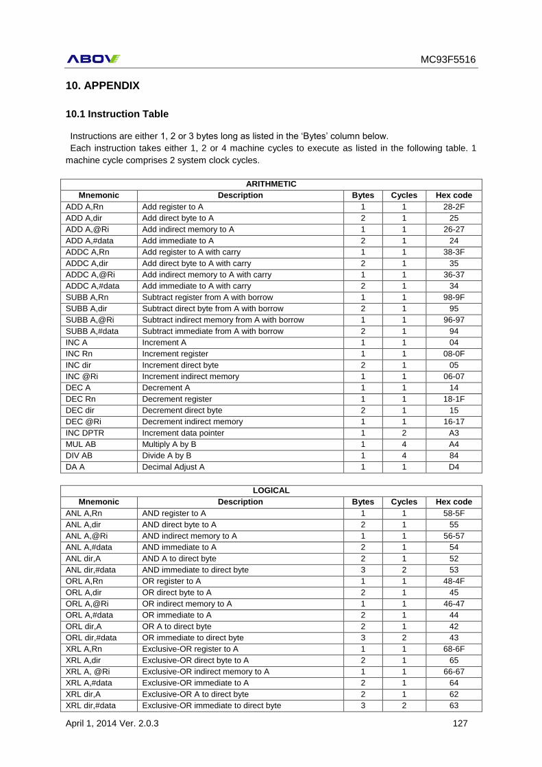
MC93F5516
April 1, 2014 Ver. 2.0.3 127
10. APPENDIX
10.1 Instruction Table
Instructions are either 1, 2 or 3 bytes long as listed in the ‘Bytes’ column below.
Each instruction takes either 1, 2 or 4 machine cycles to execute as listed in the following table. 1
machine cycle comprises 2 system clock cycles.
ARITHMETIC
Mnemonic Description Bytes Cycles Hex code
ADD A,Rn Add register to A 1 1 28-2F
ADD A,dir Add direct byte to A 2 1 25
ADD A,@Ri Add indirect memory to A 1 1 26-27
ADD A,#data Add immediate to A 2 1 24
ADDC A,Rn Add register to A with carry 1 1 38-3F
ADDC A,dir Add direct byte to A with carry 2 1 35
ADDC A,@Ri Add indirect memory to A with carry 1 1 36-37
ADDC A,#data Add immediate to A with carry 2 1 34
SUBB A,Rn Subtract register from A with borrow 1 1 98-9F
SUBB A,dir Subtract direct byte from A with borrow 2 1 95
SUBB A,@Ri Subtract indirect memory from A with borrow 1 1 96-97
SUBB A,#data Subtract immediate from A with borrow 2 1 94
INC A Increment A 1 1 04
INC Rn Increment register 1 1 08-0F
INC dir Increment direct byte 2 1 05
INC @Ri Increment indirect memory 1 1 06-07
DEC A Decrement A 1 1 14
DEC Rn Decrement register 1 1 18-1F
DEC dir Decrement direct byte 2 1 15
DEC @Ri Decrement indirect memory 1 1 16-17
INC DPTR Increment data pointer 1 2 A3
MUL AB Multiply A by B 1 4 A4
DIV AB Divide A by B 1 4 84
DA A Decimal Adjust A 1 1 D4
LOGICAL
Mnemonic Description Bytes Cycles Hex code
ANL A,Rn AND register to A 1 1 58-5F
ANL A,dir AND direct byte to A 2 1 55
ANL A,@Ri AND indirect memory to A 1 1 56-57
ANL A,#data AND immediate to A 2 1 54
ANL dir,A AND A to direct byte 2 1 52
ANL dir,#data AND immediate to direct byte 3 2 53
ORL A,Rn OR register to A 1 1 48-4F
ORL A,dir OR direct byte to A 2 1 45
ORL A,@Ri OR indirect memory to A 1 1 46-47
ORL A,#data OR immediate to A 2 1 44
ORL dir,A OR A to direct byte 2 1 42
ORL dir,#data OR immediate to direct byte 3 2 43
XRL A,Rn Exclusive-OR register to A 1 1 68-6F
XRL A,dir Exclusive-OR direct byte to A 2 1 65
XRL A, @Ri Exclusive-OR indirect memory to A 1 1 66-67
XRL A,#data Exclusive-OR immediate to A 2 1 64
XRL dir,A Exclusive-OR A to direct byte 2 1 62
XRL dir,#data Exclusive-OR immediate to direct byte 3 2 63
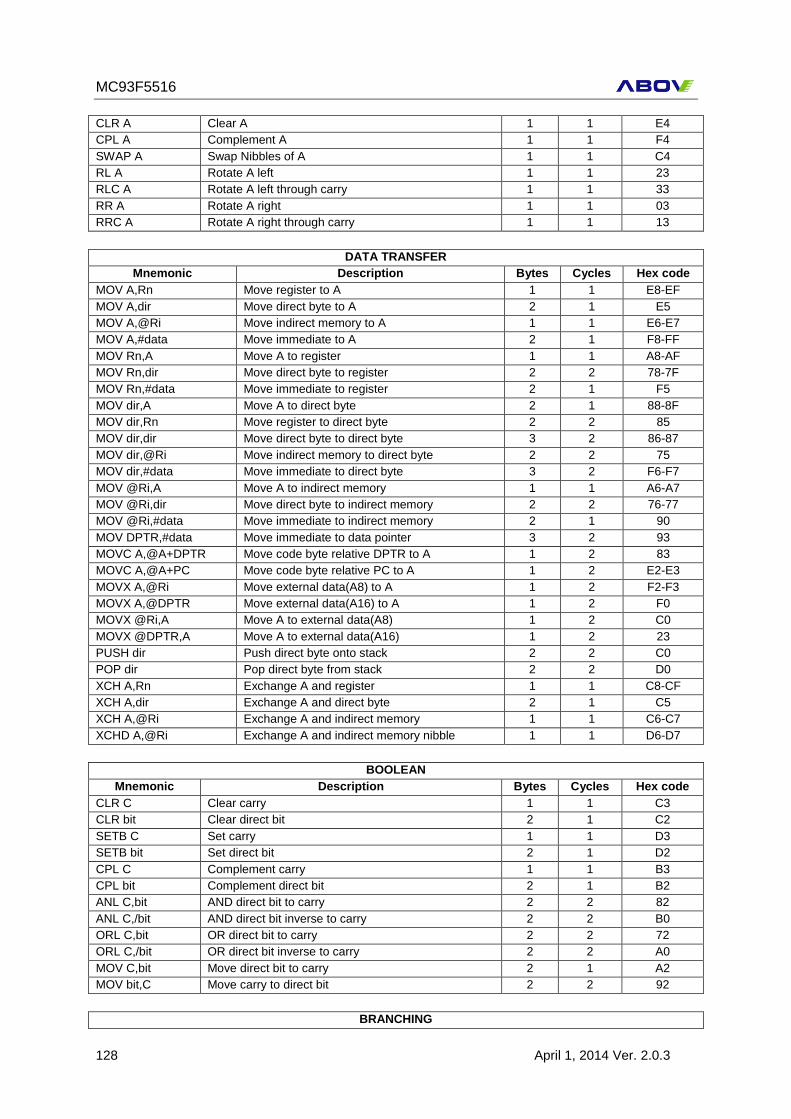
MC93F5516
128 April 1, 2014 Ver. 2.0.3
CLR A Clear A 1 1 E4
CPL A Complement A 1 1 F4
SWAP A Swap Nibbles of A 1 1 C4
RL A Rotate A left 1 1 23
RLC A Rotate A left through carry 1 1 33
RR A Rotate A right 1 1 03
RRC A Rotate A right through carry 1 1 13
DATA TRANSFER
Mnemonic Description Bytes Cycles Hex code
MOV A,Rn Move register to A 1 1 E8-EF
MOV A,dir Move direct byte to A 2 1 E5
MOV A,@Ri Move indirect memory to A 1 1 E6-E7
MOV A,#data Move immediate to A 2 1 F8-FF
MOV Rn,A Move A to register 1 1 A8-AF
MOV Rn,dir Move direct byte to register 2 2 78-7F
MOV Rn,#data Move immediate to register 2 1 F5
MOV dir,A Move A to direct byte 2 1 88-8F
MOV dir,Rn Move register to direct byte 2 2 85
MOV dir,dir Move direct byte to direct byte 3 2 86-87
MOV dir,@Ri Move indirect memory to direct byte 2 2 75
MOV dir,#data Move immediate to direct byte 3 2 F6-F7
MOV @Ri,A Move A to indirect memory 1 1 A6-A7
MOV @Ri,dir Move direct byte to indirect memory 2 2 76-77
MOV @Ri,#data Move immediate to indirect memory 2 1 90
MOV DPTR,#data Move immediate to data pointer 3 2 93
MOVC A,@A+DPTR Move code byte relative DPTR to A 1 2 83
MOVC A,@A+PC Move code byte relative PC to A 1 2 E2-E3
MOVX A,@Ri Move external data(A8) to A 1 2 F2-F3
MOVX A,@DPTR Move external data(A16) to A 1 2 F0
MOVX @Ri,A Move A to external data(A8) 1 2 C0
MOVX @DPTR,A Move A to external data(A16) 1 2 23
PUSH dir Push direct byte onto stack 2 2 C0
POP dir Pop direct byte from stack 2 2 D0
XCH A,Rn Exchange A and register 1 1 C8-CF
XCH A,dir Exchange A and direct byte 2 1 C5
XCH A,@Ri Exchange A and indirect memory 1 1 C6-C7
XCHD A,@Ri Exchange A and indirect memory nibble 1 1 D6-D7
BOOLEAN
Mnemonic Description Bytes Cycles Hex code
CLR C Clear carry 1 1 C3
CLR bit Clear direct bit 2 1 C2
SETB C Set carry 1 1 D3
SETB bit Set direct bit 2 1 D2
CPL C Complement carry 1 1 B3
CPL bit Complement direct bit 2 1 B2
ANL C,bit AND direct bit to carry 2 2 82
ANL C,/bit AND direct bit inverse to carry 2 2 B0
ORL C,bit OR direct bit to carry 2 2 72
ORL C,/bit OR direct bit inverse to carry 2 2 A0
MOV C,bit Move direct bit to carry 2 1 A2
MOV bit,C Move carry to direct bit 2 2 92
BRANCHING
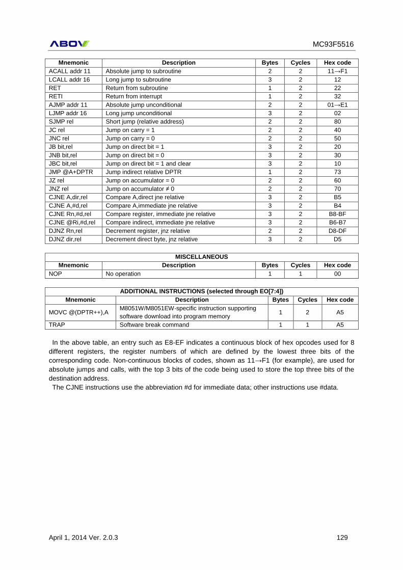
MC93F5516
April 1, 2014 Ver. 2.0.3 129
Mnemonic Description Bytes Cycles Hex code
ACALL addr 11 Absolute jump to subroutine 2 2 11→F1
LCALL addr 16 Long jump to subroutine 3 2 12
RET Return from subroutine 1 2 22
RETI Return from interrupt 1 2 32
AJMP addr 11 Absolute jump unconditional 2 2 01→E1
LJMP addr 16 Long jump unconditional 3 2 02
SJMP rel Short jump (relative address) 2 2 80
JC rel Jump on carry = 1 2 2 40
JNC rel Jump on carry = 0 2 2 50
JB bit,rel Jump on direct bit = 1 3 2 20
JNB bit,rel Jump on direct bit = 0 3 2 30
JBC bit,rel Jump on direct bit = 1 and clear 3 2 10
JMP @A+DPTR Jump indirect relative DPTR 1 2 73
JZ rel Jump on accumulator = 0 2 2 60
JNZ rel Jump on accumulator ≠ 0 2 2 70
CJNE A,dir,rel Compare A,direct jne relative 3 2 B5
CJNE A,#d,rel Compare A,immediate jne relative 3 2 B4
CJNE Rn,#d,rel Compare register, immediate jne relative 3 2 B8-BF
CJNE @Ri,#d,rel Compare indirect, immediate jne relative 3 2 B6-B7
DJNZ Rn,rel Decrement register, jnz relative 2 2 D8-DF
DJNZ dir,rel Decrement direct byte, jnz relative 3 2 D5
MISCELLANEOUS
Mnemonic Description Bytes Cycles Hex code
NOP No operation 1 1 00
ADDITIONAL INSTRUCTIONS (selected through EO[7:4])
Mnemonic Description Bytes Cycles Hex code
MOVC @(DPTR++),A M8051W/M8051EW-specific instruction supporting
software download into program memory 1 2 A5
TRAP Software break command 1 1 A5
In the above table, an entry such as E8-EF indicates a continuous block of hex opcodes used for 8
different registers, the register numbers of which are defined by the lowest three bits of the
corresponding code. Non-continuous blocks of codes, shown as 11→F1 (for example), are used for
absolute jumps and calls, with the top 3 bits of the code being used to store the top three bits of the
destination address.
The CJNE instructions use the abbreviation #d for immediate data; other instructions use #data.
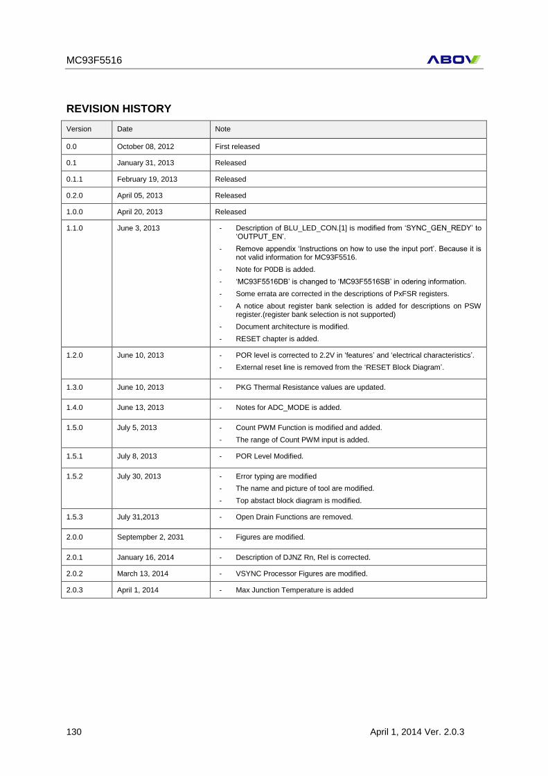
MC93F5516
130 April 1, 2014 Ver. 2.0.3
REVISION HISTORY
Version Date Note
0.0 October 08, 2012 First released
0.1 January 31, 2013 Released
0.1.1 February 19, 2013 Released
0.2.0 April 05, 2013 Released
1.0.0 April 20, 2013 Released
1.1.0 June 3, 2013 - Description of BLU_LED_CON.[1] is modified from ‘SYNC_GEN_REDY’ to ‘OUTPUT_EN’.
- Remove appendix ‘Instructions on how to use the input port’. Because it is not valid information for MC93F5516.
- Note for P0DB is added.
- ‘MC93F5516DB’ is changed to ‘MC93F5516SB’ in odering information.
- Some errata are corrected in the descriptions of PxFSR registers.
- A notice about register bank selection is added for descriptions on PSW register.(register bank selection is not supported)
- Document architecture is modified.
- RESET chapter is added.
1.2.0 June 10, 2013 - POR level is corrected to 2.2V in ‘features’ and ‘electrical characteristics’.
- External reset line is removed from the ‘RESET Block Diagram’.
1.3.0 June 10, 2013 - PKG Thermal Resistance values are updated.
1.4.0 June 13, 2013 - Notes for ADC_MODE is added.
1.5.0 July 5, 2013 - Count PWM Function is modified and added.
- The range of Count PWM input is added.
1.5.1 July 8, 2013 - POR Level Modified.
1.5.2 July 30, 2013 - Error typing are modified
- The name and picture of tool are modified.
- Top abstact block diagram is modified.
1.5.3 July 31,2013 - Open Drain Functions are removed.
2.0.0 Septempber 2, 2031 - Figures are modified.
2.0.1 January 16, 2014 - Description of DJNZ Rn, Rel is corrected.
2.0.2 March 13, 2014 - VSYNC Processor Figures are modified.
2.0.3 April 1, 2014 - Max Junction Temperature is added

MC93F5516
April 1, 2014 Ver. 2.0.3 131

MC93F5516
132 April 1, 2014 Ver. 2.0.3
Table of Contents
1. Overview ............................................................................................................................................. 2
1.1 Description .................................................................................................................................... 2
1.2 Features ........................................................................................................................................ 2
1.3 Ordering Information ..................................................................................................................... 3
1.4 Development Tools ....................................................................................................................... 3
1.4.1 Compiler ................................................................................................................................ 3
1.4.2 OCD II Emulator and Debugger ............................................................................................ 3
1.4.3 Programmer........................................................................................................................... 4
1.5 Block Diagram .............................................................................................................................. 5
1.6 PIN Assignment ............................................................................................................................ 6
1.6.1 24-QFN .................................................................................................................................. 6
1.6.2 24 SSOP ................................................................................................................................ 7
1.7 Pin Description .............................................................................................................................. 8
1.8 Package Dimension ...................................................................................................................... 9
1.8.1 24 QFN Package Dimension ................................................................................................. 9
1.8.2 24 SSOP Package Dimension ............................................................................................ 10
2. Ports .................................................................................................................................................. 11
2.1 Port Register ............................................................................................................................... 11
2.1.1 Data Register (PxDA) .......................................................................................................... 11
2.1.2 Direction Register (PxDIR) .................................................................................................. 11
2.1.3 Pull-up Resistor Selection Register (PxPU) ........................................................................ 11
2.1.4 Debounce Enable Register (PxDB) ..................................................................................... 11
2.1.5 Port Function Selection Register (PxFSR) .......................................................................... 13
2.2 Register Map .............................................................................................................................. 14
2.3 Register description of P0 ........................................................................................................... 14
2.4 Register description for P1 ......................................................................................................... 16
2.5 Register description for P2 ......................................................................................................... 18
2.6 I/O Port Sturcture ........................................................................................................................ 21
2.6.1 P0[0,1,5,6,7]/P1[0,1],P2[0] Port Structure ........................................................................... 21
2.6.2 P0[1,3,4] Port Structure ....................................................................................................... 22
2.6.3 P1[4,5,6] Port Structure ....................................................................................................... 23
2.6.4 P1[2,3,7] / P2[1,2,3,4,5] Port Structure ............................................................................... 24
3. Memory ............................................................................................................................................. 25
3.1 Program Memory ........................................................................................................................ 25
3.2 Internal Data Memory ................................................................................................................. 26
3.3 External Data Memory ................................................................................................................ 27
3.4 SFR Map ..................................................................................................................................... 28
3.4.1 SFR Map Summary ............................................................................................................. 28
3.4.2 XSFR Map Summary .......................................................................................................... 29
3.4.3 Compiler Compatible SFR ................................................................................................... 30
MC93F5516
April 1, 2014 Ver. 2.0.3 133
4. Interrupt Controller ............................................................................................................................ 32
4.1 Overview ..................................................................................................................................... 32
4.2 Block Diagram ............................................................................................................................ 32
4.3 Interrupt Vector Table ................................................................................................................. 33
4.4 Interrupt Sequence ..................................................................................................................... 33
4.5 Effective Timing after Controlling Interrupt bit ............................................................................ 35
4.6 Interrupt Enable Accept Timing .................................................................................................. 36
4.7 Interrupt Service Routine Address .............................................................................................. 36
4.8 Saving/Restore General-Purpose Registers .............................................................................. 36
4.9 Interrupt Timing ........................................................................................................................... 37
4.10 External Interrupt ...................................................................................................................... 37
4.11 Interrupt Register ...................................................................................................................... 38
4.11.1 Interrupt Enable Register (IEN0, IEN1) ............................................................................. 38
4.11.2 Interrupt Requeset Register (IRQ0, IRQ1) ........................................................................ 38
4.12 Register Map ............................................................................................................................ 38
4.13 Register description for Interrupt .............................................................................................. 39
5. Clock Control and Power Saving ...................................................................................................... 44
5.1 Clock Generator .......................................................................................................................... 44
5.1.1 Overview .............................................................................................................................. 44
5.1.2 Block Diagram ..................................................................................................................... 44
5.1.3 Register Map ....................................................................................................................... 44
5.1.4 Register description for Clock Generator ............................................................................ 44
5.2 Power Down Operation ............................................................................................................... 46
5.2.1 Peripheral Operations in SLEEP1 and SLEEP2 Mode ...................................................... 46
5.2.2 SLEEP1 mode ..................................................................................................................... 46
5.2.3 SLEEP2 mode ..................................................................................................................... 46
5.2.4 Register Map ....................................................................................................................... 47
5.2.5 Register description for Power Down Operation ................................................................. 47
6. RESET .............................................................................................................................................. 48
6.1 Overview ..................................................................................................................................... 48
6.2 Reset Source .............................................................................................................................. 48
6.3 Reset Procedure ......................................................................................................................... 48
6.4 Power On Reset ......................................................................................................................... 49
7. Peripherals ........................................................................................................................................ 50
7.1 Watch Dog Timer ........................................................................................................................ 50
7.1.1 Overview .............................................................................................................................. 50
7.1.2 Register Map ....................................................................................................................... 50
7.1.3 Register description for Watch Dog Timer .......................................................................... 51
7.1.4 WDT Interrupt Timing Waveform......................................................................................... 52
7.2 TIMER ......................................................................................................................................... 53
7.2.1 16-bit TIMER 0 .................................................................................................................... 53
7.2.2 8-bit TIMER 1 ...................................................................................................................... 58
7.3 I2C .............................................................................................................................................. 62
MC93F5516
134 April 1, 2014 Ver. 2.0.3
7.3.1 Overview .............................................................................................................................. 62
7.3.2 Block Diagram ..................................................................................................................... 62
7.3.3 I2C Bit Transfer ................................................................................................................... 62
7.3.4 START / REPEATED START / STOP ................................................................................ 63
7.3.5 DATA TRANSFER .............................................................................................................. 63
7.3.6 ACKNOWLEDGE ................................................................................................................ 64
7.3.7 SYNCHRONIZATION / ARBITRATION .............................................................................. 64
7.3.8 OPERATION ....................................................................................................................... 65
7.3.9 Register Map ....................................................................................................................... 73
7.3.10 I2C Register description .................................................................................................... 73
7.3.11 Register description for I2C ............................................................................................... 73
7.4 SPI .............................................................................................................................................. 77
7.4.1 SPI Slave ............................................................................................................................. 77
7.4.2 SPI MASTER ....................................................................................................................... 84
7.5 8-Bit A/D Converter ..................................................................................................................... 92
7.5.1 Overview .............................................................................................................................. 92
7.5.2 Block Diagram ..................................................................................................................... 92
7.5.3 ADC Operation .................................................................................................................... 93
7.5.4 Register Map ....................................................................................................................... 94
7.5.5 ADC Register description .................................................................................................... 94
7.5.6 Register description for ADC ............................................................................................... 94
7.6 Counter PWM ............................................................................................................................. 96
7.6.1 Overview .............................................................................................................................. 96
7.6.2 Block Diagram ..................................................................................................................... 96
7.6.3 Function Description ............................................................................................................ 96
7.7 Calculator .................................................................................................................................. 101
7.7.1 Overview ............................................................................................................................ 101
7.7.2 Block Diagram ................................................................................................................... 101
7.7.3 Function Description .......................................................................................................... 102
7.8 SYNC Processor ....................................................................................................................... 107
7.8.2 Block Diagram ................................................................................................................... 107
7.8.3 Function Description .......................................................................................................... 108
7.8.4 SFR MAP of the VSYNC Processor .................................................................................. 108
7.8.5 SFR Description ................................................................................................................ 109
7.9 PWM OUT Controller ................................................................................................................ 113
7.9.1 Block Diagram ................................................................................................................... 113
7.9.2 Function Description .......................................................................................................... 113
7.9.3 SFR MAP of the LED Controller ........................................................................................ 114
8. Memory Programming ..................................................................................................................... 116
8.1 Overview ................................................................................................................................... 116
8.1.1 Description ......................................................................................................................... 116
8.1.2 Features ............................................................................................................................ 116
8.2 Flash and EEPROM Control and status register ...................................................................... 116
MC93F5516
April 1, 2014 Ver. 2.0.3 135
8.2.1 Register Map ..................................................................................................................... 116
8.2.2 Register description for Flash and EEPROM .................................................................... 117
9. Electrical Characteristics ................................................................................................................. 121
9.1 Absolute Maximum Ratings ...................................................................................................... 121
9.2 Recommended Operating Conditions ...................................................................................... 121
9.3 A/D Converter Characteristics .................................................................................................. 122
9.4 Voltage Dropout Converter Characteristics .............................................................................. 122
9.5 Power-On Reset Characteristics .............................................................................................. 123
9.6 DC Characteristics .................................................................................................................... 123
9.7 AC Characteristics .................................................................................................................... 124
9.8 SPI Characteristics ................................................................................................................... 125
9.9 PKG Themal Resistance values ............................................................................................... 126
10. APPENDIX .................................................................................................................................... 127
10.1 Instruction Table ..................................................................................................................... 127
REVISION HISTORY .......................................................................................................................... 130
Table of Contents ................................................................................................................................ 132
List of Figures ...................................................................................................................................... 136
List of Tables ....................................................................................................................................... 139
MC93F5516
136 April 1, 2014 Ver. 2.0.3
List of Figures
Figure 1-1 OCD II Debugger and Pin Configuration ................................................................................................. 3
Figure 1-2 S-PGM + BLU (Single Writer) ......................................................................................................................... 4
Figure 1-3 Gang Programmer ............................................................................................................................................... 4
Figure 1-4 Top Abstract Block Diagram ........................................................................................................................... 5
Figure 1-5 24-QFN PIN Assignment Diagram ............................................................................................................... 6
Figure 1-6 24 SSOP PIN Assignment Diagram ............................................................................................................. 7
Figure 1-7. 24-QFN Package Dimension .......................................................................................................................... 9
Figure 1-8. 24-SSOP Package Dimension ..................................................................................................................... 10
Figure 2-1 Debounce Function .......................................................................................................................................... 11
Figure 2-2 General Purpose I/O Port Structure with Debounce Circuit ......................................................... 21
Figure 2-3 Dual VIH/VIL Port Structure with Debounce Circuit ......................................................................... 22
Figure 2-4 ADC Port Structure ........................................................................................................................................... 23
Figure 2-5 Nomal General Purpose I/O Port Structure with Debounce Circuit ......................................... 24
Figure 3-1 Program memory .............................................................................................................................................. 25
Figure 3-2 Internal data memory map .......................................................................................................................... 26
Figure 3-3 Lower 128 bytes RAM ..................................................................................................................................... 27
Figure 3-4 X-Data Memory ................................................................................................................................................. 27
Figure 4-1 Block Diagram of Interrupt ........................................................................................................................... 32
Figure 4-2 Interrupt Vector Address Table .................................................................................................................. 34
Figure 4-3 Interrupt flag result effective Timing ....................................................................................................... 35
Figure 4-4 Interrupt Enable Register effective Timing ........................................................................................... 35
Figure 4-5 Interrupt Response Timing Diagram ........................................................................................................ 36
Figure 4-6 Correspondence between vector Table address and the entry address of ISP .................. 36
Figure 4-7 Saving/Restore Process Diagram & Sample Source ........................................................................ 36
Figure 4-8 Timing chart of Interrupt Acceptance and Interrupt Return Instruction ................................ 37
Figure 4-9 External Interrupt Description ..................................................................................................................... 37
Figure 5-1 Clock Generator Block Diagram ................................................................................................................. 44
Figure 5-2 Clock Chagne Sequence ................................................................................................................................ 45
Figure 5-3 SLEEP1, 2 Mode Release Timing by External Interrupt ................................................................... 47
Figure 6-1 RESET Block Diagram ...................................................................................................................................... 48
Figure 6-2 RESET Timing Diagram ................................................................................................................................... 49
Figure 6-3 POR Reset Diagram ......................................................................................................................................... 49
MC93F5516
April 1, 2014 Ver. 2.0.3 137
Figure 7-1 Block diagram of the Watch Dog Timer ................................................................................................ 50
Figure 7-2 TIMER 0 Block Diagram ................................................................................................................................. 53
Figure 7-3 The Interrupt of TIMER 0 .............................................................................................................................. 54
Figure 7-4 Operation Example of TIMER 0 .................................................................................................................. 54
Figure 7-5 Express Timer Overflow and Interrupt in Capture Mode ............................................................. 55
Figure 7-6 TIMER 1 Block Diagram ................................................................................................................................. 58
Figure 7-7 The Intterupt of TIMER 1............................................................................................................................... 59
Figure 7-8 Operation Example of TIMER 1 .................................................................................................................. 59
Figure 7-9 Example of PWM ............................................................................................................................................... 60
Figure 7-10 I2C Block Diagram ......................................................................................................................................... 62
Figure 7-11 Bit Transfer on the I2C-Bus ....................................................................................................................... 63
Figure 7-12 START and STOP Condition ....................................................................................................................... 63
Figure 7-13 Data Transfer on the I2C-Bus ................................................................................................................... 64
Figure 7-14 Acknowledge on the I2C-Bus ................................................................................................................... 64
Figure 7-15 Clock Synchronization during Arbitration Procedure .................................................................... 65
Figure 7-16 Arbitration Procedure of Two Masters ................................................................................................. 65
Figure 7-17 Formats and States in the Master Transmitter Mode ................................................................... 67
Figure 7-18 Formats and States in the Master Receiver Mode ......................................................................... 69
Figure 7-19 Formats and States in the Slave Transmitter Mode ...................................................................... 71
Figure 7-20 Formats and States in the Slave Receiver Mode ............................................................................. 72
Figure 7-21 SPI Slave Block Diagram ............................................................................................................................. 77
Figure 7-22 SPI Slave Operating Timing ....................................................................................................................... 79
Figure 7-23 SPI Slave Signal Diagram ............................................................................................................................ 79
Figure 7-24 SPI Master Block Diagram .......................................................................................................................... 84
Figure 7-25 SPI Master Operating Wave Diagram ................................................................................................... 85
Figure 7-26 A/D Converter Block Diagram .................................................................................................................. 92
Figure 7-27 A/D Analog Input Pin Connecting Capacitor .................................................................................... 93
Figure 7-28 A/D Converter Operation Flow ................................................................................................................ 93
Figure 7-29 Block Diagram of PWM Counter ............................................................................................................. 96
Figure 7-30 Counter PWM Operating Wave Diagram ........................................................................................... 97
Figure 7-31 Calculator Block Diagram ......................................................................................................................... 101
Figure 7-32 SYNC Processor Block Diagram ............................................................................................................. 107
Figure 7-33 PWM OUT Controller Block Diagram.................................................................................................. 113
Figure 9-1 AC Timing ........................................................................................................................................................... 124
Figure 9-2 SPI Timing ........................................................................................................................................................... 125

MC93F5516
138 April 1, 2014 Ver. 2.0.3

MC93F5516
April 1, 2014 Ver. 2.0.3 139
List of Tables
Table 1.1 Order Inforrmation __________________________________________________________________________ 3
Table 1.2 Pin Description ______________________________________________________________________________ 8
Table 2.1 Debounce Table ___________________________________________________________________________ 12
Table 2.2 PxFSR Description Table ___________________________________________________________________ 13
Table 2.3 Register map ______________________________________________________________________________ 14
Table 3.1 SFR Map Summary ________________________________________________________________________ 28
Table 3.2 SFR Map Summary ________________________________________________________________________ 29
Table 4.1 Interrupt Vector Address Table ___________________________________________________________ 33
Table 4.2 Interrupt Register Map ____________________________________________________________________ 38
Table 5.1 Clock Generator Register Map ____________________________________________________________ 44
Table 5.2 Peripheral Operation during SLEEP. _______________________________________________________ 46
Table 5.3 PCON Register Map _______________________________________________________________________ 47
Table 6-1 Reset State ________________________________________________________________________________ 48
Table 7.1 WDT Register Map ________________________________________________________________________ 50
Table 7.2 Timer 0 Register Map _____________________________________________________________________ 55
Table 7.3 Timer 1 Register Map _____________________________________________________________________ 61
Table 7.4 SPI Slave Register Map ____________________________________________________________________ 80
Table 7.5 SPI Master Register Map __________________________________________________________________ 86
Table 7.6 ADC Register Map _________________________________________________________________________ 94
Table 7.7 CNT_PWM_CDIV Table ____________________________________________________________________ 97
Table 7.8 Counter PWM Register Map ______________________________________________________________ 98
Table 7.9 Calculator Register Map __________________________________________________________________ 103
Table 7.10 VSYNG Processor SFR Map _____________________________________________________________ 108
Table 7.11 SET & CLR Register Upating Description _______________________________________________ 113
Table 7.12 SFR Map of the PWM Out Controller __________________________________________________ 114
Table 8.1 Register Map _____________________________________________________________________________ 116
Table 9.1 Absolute Maximum Ratings ______________________________________________________________ 121
Table 9.2 Recommended Operation Conditions ___________________________________________________ 121
Table 9.3 A/D Converter Characteristics ____________________________________________________________ 122
Table 9.4 Voltage Dropout Converter Characteristics ______________________________________________ 122
Table 9.5 Power-On Reset Characteristics __________________________________________________________ 123
Table 9.6 DC Characteristics ________________________________________________________________________ 123
MC93F5516
140 April 1, 2014 Ver. 2.0.3
Table 9.7 AC Characteristics ________________________________________________________________________ 124
Table 9.8 SPI Characteristics ________________________________________________________________________ 125
Table 9.9 PKG Themal Resistance Table ____________________________________________________________ 126