may 2011 revised june 2011 buck pfc controller startup from the ac line limiting eliminates the need...
TRANSCRIPT

11
9
NC
BIASSNS
12 BIASCTRL
LINESNS
4
VDD
1
TST
10
PFCDRV
13
3CS
5CS
2VBULK
7 6 14 8
NC REFIN VSS FAULT
UCC29910APW
BIAS
SUPPLY
DRIVER
EMC
FILTER
HS BULK
SENSE
VAC
VBULK
UCC29910A
www.ti.com SLUSAK8A –MAY 2011–REVISED JUNE 2011
Buck PFC ControllerCheck for Samples: UCC29910A
1FEATURES DESCRIPTIONThe UCC29910A Buck Power Factor Correction• Buck Power Factor Correction for High(PFC) controller provides a relatively flatEfficiency Across Linehigh-efficiency performance across universal line for• Low Off-Line Startup Current, With SmartStartdesigners requiring a high power factor (>0.9) andAlgorithm for Fast Startup With Soft-Startwishing to meet the requirements of IEC 61000-3-2.• Compatible With Resistive or Pass Transistor Based on a buck topology, inherent inrush current
Fed Startup from the AC Line limiting eliminates the need for additional• Low Power SmartBurst Mode for Standby and components. With a typical bus voltage of 84 V, the
Light-Load Conditions topology is ideally suited for use with low voltagestress downstream regulation/isolation power trains,• Current Sense Inputs for PFC control andsuch as half-bridge stages controlled by theOverload ProtectionUCC29900, (Texas Instruments Literature Number,• Line Sense UVLOSLUS923). This combination offers low• Sense and Drive Control for External Startupcommon-mode noise generation allowing reducedDepletion Mode FETfiltering and exceptionally high conversion efficiency.
• Latching Fault Input PinThe UCC29910A incorporates AC line UVLO andcontrolled soft start for fast start-up. EnhancedAPPLICATIONSlight-load efficiency is achieved through advanced
• High Efficiency AC-DC Adapters management algorithms for best-in-class no-load and• Low Profile and High Density Adapters light-load performance.
SIMPLIFIED APPLICATION DIAGRAM
1
Please be aware that an important notice concerning availability, standard warranty, and use in critical applications of TexasInstruments semiconductor products and disclaimers thereto appears at the end of this data sheet.
PRODUCTION DATA information is current as of publication date. Copyright © 2011, Texas Instruments IncorporatedProducts conform to specifications per the terms of the TexasInstruments standard warranty. Production processing does notnecessarily include testing of all parameters.

UCC29910A
SLUSAK8A –MAY 2011–REVISED JUNE 2011 www.ti.com
This integrated circuit can be damaged by ESD. Texas Instruments recommends that all integrated circuits be handled withappropriate precautions. Failure to observe proper handling and installation procedures can cause damage.
ESD damage can range from subtle performance degradation to complete device failure. Precision integrated circuits may be moresusceptible to damage because very small parametric changes could cause the device not to meet its published specifications.
ORDERING INFORMATIONPART NUMBER PACKAGE PACKING
UCC29910APW Plastic, 14-Pin TSSOP (PW) 90-Pc. Tube
UCC29910APWR Plastic, 14-Pin TSSOP (PW) 2000-Pc. Tape and Reel
ABSOLUTE MAXIMUM RATINGSover operating free-air temperature range (unless otherwise noted) (1) (2) (3)
VALUE UNIT
4.1VDD Supply Voltage
-0.3 V
Voltage: All pins −0.3 to VDD + 0.3
TA Operating free air temperature, (4)
−40 to 105TJ Operational junction temperature, (4)
°CTSTG Storage temperature (4) −40 to 105
Lead temperature (10 seconds) 260
(1) These are stress limits. Stress beyond these limits may cause permanent damage to the device. Functional operation of the device atthese or any conditions beyond those indicated under RECOMMENDED OPERATING CONDITIONS is not implied. Exposure toabsolute maximum rated conditions for extended periods of time may affect device reliability.
(2) All voltages are with respect to VSS.(3) All currents are positive into the terminal, negative out of the terminal.(4) Higher temperature may be applied during board soldering process according to the current JEDEC J-STD-020 specification with peak
reflow temperatures not higher than classified on the device label on the shipping boxes or reels.
THERMAL INFORMATION
THERMAL METRIC (1) UNITSPINS
θJA Junction-to-ambient thermal resistance (2)
θJCtop Junction-to-case (top) thermal resistance (3)
θJB Junction-to-board thermal resistance (4)
°C/WψJT Junction-to-top characterization parameter (5)
ψJB Junction-to-board characterization parameter (6)
θJCbot Junction-to-case (bottom) thermal resistance (7)
(1) For more information about traditional and new thermal metrics, see the IC Package Thermal Metrics application report, SPRA953.(2) The junction-to-ambient thermal resistance under natural convection is obtained in a simulation on a JEDEC-standard, high-K board, as
specified in JESD51-7, in an environment described in JESD51-2a.(3) The junction-to-case (top) thermal resistance is obtained by simulating a cold plate test on the package top. No specific
JEDEC-standard test exists, but a close description can be found in the ANSI SEMI standard G30-88.(4) The junction-to-board thermal resistance is obtained by simulating in an environment with a ring cold plate fixture to control the PCB
temperature, as described in JESD51-8.(5) The junction-to-top characterization parameter, ψJT, estimates the junction temperature of a device in a real system and is extracted
from the simulation data for obtaining θJA, using a procedure described in JESD51-2a (sections 6 and 7).(6) The junction-to-board characterization parameter, ψJB, estimates the junction temperature of a device in a real system and is extracted
from the simulation data for obtaining θJA , using a procedure described in JESD51-2a (sections 6 and 7).(7) The junction-to-case (bottom) thermal resistance is obtained by simulating a cold plate test on the exposed (power) pad. No specific
JEDEC standard test exists, but a close description can be found in the ANSI SEMI standard G30-88.
2 Submit Documentation Feedback Copyright © 2011, Texas Instruments Incorporated
Product Folder Link(s): UCC29910A
UCC29910A
www.ti.com SLUSAK8A –MAY 2011–REVISED JUNE 2011
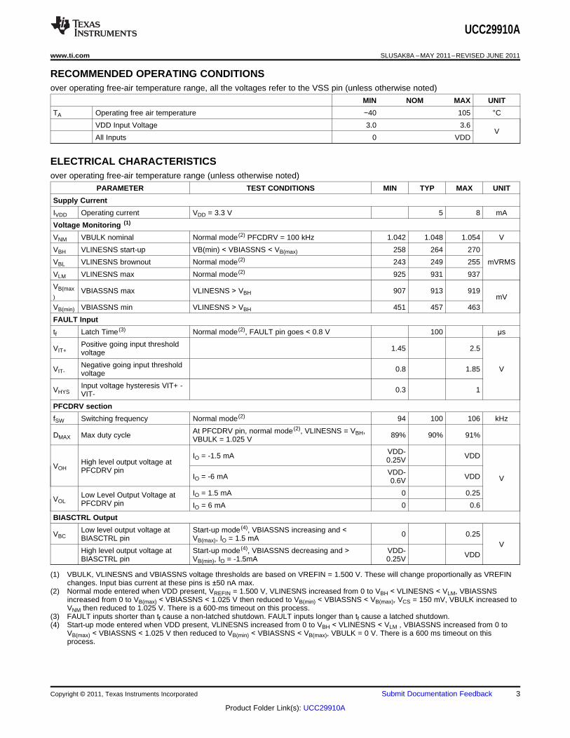
RECOMMENDED OPERATING CONDITIONSover operating free-air temperature range, all the voltages refer to the VSS pin (unless otherwise noted)
MIN NOM MAX UNIT
TA Operating free air temperature −40 105 °CVDD Input Voltage 3.0 3.6
VAll Inputs 0 VDD
ELECTRICAL CHARACTERISTICSover operating free-air temperature range (unless otherwise noted)
PARAMETER TEST CONDITIONS MIN TYP MAX UNIT
Supply Current
IVDD Operating current VDD = 3.3 V 5 8 mA
Voltage Monitoring (1)
VNM VBULK nominal Normal mode (2) PFCDRV = 100 kHz 1.042 1.048 1.054 V
VBH VLINESNS start-up VB(min) < VBIASSNS < VB(max) 258 264 270
VBL VLINESNS brownout Normal mode (2) 243 249 255 mVRMS
VLM VLINESNS max Normal mode (2) 925 931 937
VB(max VBIASSNS max VLINESNS > VBH 907 913 919) mVVB(min) VBIASSNS min VLINESNS > VBH 451 457 463
FAULT Input
tf Latch Time (3) Normal mode (2), FAULT pin goes < 0.8 V 100 µs
Positive going input thresholdVIT+ 1.45 2.5voltage
Negative going input thresholdVIT- 0.8 1.85 Vvoltage
Input voltage hysteresis VIT+ -VHYS 0.3 1VIT-
PFCDRV section
fSW Switching frequency Normal mode (2) 94 100 106 kHz
At PFCDRV pin, normal mode (2), VLINESNS = VBH,DMAX Max duty cycle 89% 90% 91%VBULK = 1.025 V
VDD-IO = -1.5 mA VDD0.25VHigh level output voltage atVOH PFCDRV pin VDD-IO = -6 mA VDD V0.6V
IO = 1.5 mA 0 0.25Low Level Output Voltage atVOL PFCDRV pin IO = 6 mA 0 0.6
BIASCTRL Output
Low level output voltage at Start-up mode (4), VBIASSNS increasing and <VBC 0 0.25BIASCTRL pin VB(max), IO = 1.5 mAV
High level output voltage at Start-up mode (4), VBIASSNS decreasing and > VDD- VDDBIASCTRL pin VB(min), IO = -1.5mA 0.25V
(1) VBULK, VLINESNS and VBIASSNS voltage thresholds are based on VREFIN = 1.500 V. These will change proportionally as VREFINchanges. Input bias current at these pins is ±50 nA max.
(2) Normal mode entered when VDD present, VREFIN = 1.500 V, VLINESNS increased from 0 to VBH < VLINESNS < VLM, VBIASSNSincreased from 0 to VB(max) < VBIASSNS < 1.025 V then reduced to VB(min) < VBIASSNS < VB(max), VCS = 150 mV, VBULK increased toVNM then reduced to 1.025 V. There is a 600-ms timeout on this process.
(3) FAULT inputs shorter than tf cause a non-latched shutdown. FAULT inputs longer than tf cause a latched shutdown.(4) Start-up mode entered when VDD present, VLINESNS increased from 0 to VBH < VLINESNS < VLM , VBIASSNS increased from 0 to
VB(max) < VBIASSNS < 1.025 V then reduced to VB(min) < VBIASSNS < VB(max), VBULK = 0 V. There is a 600 ms timeout on thisprocess.
Copyright © 2011, Texas Instruments Incorporated Submit Documentation Feedback 3
Product Folder Link(s): UCC29910A

1
2
3
4
5
6
7
14
13
12
11
10
9
8
VDD VSS
VBULK
CS
LINESNS
CS
REFIN
NC FAULT
BIASSNS
TST
NC
BIASCTRL
PFCDRV
UCC29910A
SLUSAK8A –MAY 2011–REVISED JUNE 2011 www.ti.com
DEVICE INFORMATION
UCC29910A 14- Pin TSSOP (PW)
TERMINAL FUNCTIONSTERMINAL
I/O DESCRIPTIONNAME NO.
Provides power to the device; should be decoupled with ceramic capacitor (1 µF), connectedVDD 1 - directly across pins 1-14.
VBULK 2 I Voltage sensing of the bulk capacitor.
CS 3 I Current sense input for PFC stage.
LINESNS 4 I Rectified AC line sense input.
CS 5 I Current sense input for PFC stage.
REFIN 6 I Reference input for internal comparators/error amplifier.
NC 7 - NC, this pin is not used, and should be left open.
FAULT 8 I Fault input for over-voltage or over-load protection.
BIASSNS 9 I Sense input for the bias rail for startup control.
TST 10 I This pin should be connected directly to VDD.
NC 11 - No connection should be made to this pin.
BIASCTRL 12 O Control output for the external startup FET for startup control.
PFCDRV 13 O Drive for PFC FET.
VSS 14 - Ground for internal circuitry.
4 Submit Documentation Feedback Copyright © 2011, Texas Instruments Incorporated
Product Folder Link(s): UCC29910A

UCC29910A
www.ti.com SLUSAK8A –MAY 2011–REVISED JUNE 2011
Detailed Pin Description
Pin 1 – VDD: This pin supplies power to the device. A minimum supply voltage level of 3.0 V and maximum of3.6 V is recommended.
Pin 2 – VBULK: The output voltage level, VBULK is sensed on this pin. The HV bulk sensing network should bescaled so that the desired output voltage produces VNM at this pin. The Thevenin impedance at this pin should bebelow 20 kΩ, with appropriate capacitance provided for noise filtering.
NOTEThe VBULK scaling and LINESNS scaling must maintain a ratio of close to 4:1 to ensureoptimum operation of the SmartStart algorithm.
Pin 3 – CS: This pin senses the current in the PFC stage. Both CS pins must be connected to the current sensesignal and it is not permissible to leave one floating. The CS pins are intended to sense average low side PFCFET current directly. A 150-mΩ current sense resistor value is optimal for powers of 90 W, with appropriatescaling for higher power levels. The recommended feed impedance level is approximately 100 Ω, and a capacitorof 1 µF is also recommended to act as a filter on the input current and to minimise noise pickup. A smaller valuecapacitor may result in possible current loop instability. A larger cap value may result in poor Power Factor (PF)due to excessive current signal phase shift. UCC29910A does not provide cycle-by-cycle inductor currentlimiting. An external circuit is needed if this type of protection is required.
Pin 4 – LINESNS: This pin senses the rectified line voltage. The internal reference for this pin is internally scaledto ¼ of the VBULK reference.
NOTEThe LINESNS scaling and VBULK scaling must maintain a ratio of close to 1:4 to ensureoptimum operation of the SmartStart algorithm.
A peak of high-line voltage (typically 373-V for 264-VAC input) should be scaled to correspond to 1.158 VDC atthis pin. A pin feed impedance of less than 20 kΩ is recommended along with a filter capacitor of at least 2.2 nFfor noise filtering. The RMS voltage at this pin must be greater than VBH before PFCDRV can start switching.The PFCDRV will go low if the RMS voltage drops below the brownout level VBL (21 ms timeout). The controllerwill not start if VLINESNS exceeds VLM, (VBULK = 0 V).
Pin 5 – CS: See pin 3 description above. This pin senses the current in the PFC stage, pins 3 and 5 must beconnected together.
Pin 6 – REFIN: This pin must be connected to an external accurate 1.500 V reference source, e.g. using asuitable shunt regulator with voltage setting resistors such as TLVH431A. The reference voltage must beestablished within 100 ms after VDD reaches 3.0 V.
Pin 7 – NC: This pin is not used, and should be left open.
Copyright © 2011, Texas Instruments Incorporated Submit Documentation Feedback 5
Product Folder Link(s): UCC29910A

3
14 VSS
4
Oscillator
7
Start-up Burst
CLK
13 PFCDRV
6
9
2
CS
Gate Control
Logic
8 FAULT
“Smart-Start”
Soft Start
Burst Control
1VDD
12
1.92 V
POR+
Brown- out
Detection & Filter
Latch reset detect
5
Startup
Bias Control
CS
VBULK
BIASSNS
BIASCTRL
NC
REFIN
Fault Latch
Run/ Stop
EN
EN
Voltage Loop
PI Error Amp
REF
REF
-
+
PWM
Generator
EN
EN
BULK OV
Clamp
Disable
PFCDRV Blanking
PFC Duty Cycle
Light Load Detect
Burst Mode
Control
EN
LINESNS
10 TST
UDG-11105
UCC29910A
11
NC
UCC29910A
SLUSAK8A –MAY 2011–REVISED JUNE 2011 www.ti.com
Pin 8 – FAULT: This pin when pulled low causes PFCDRV and BIASCTRL to go low, typically within 10 us. Aftera 100 us delay the FAULT input is sampled again. If the FAULT has cleared high, the UCC29910A goes intoSmartStart mode. If the FAULT input is still low the device enters a latched shutdown state.
Pin 9 – BIASSNS: This pin is used to sense the PFC stage bias rail (normally in the 8 V to 12 V range to drivethe PFC power MOSFET) during start-up to allow control of the external start-up FET. The voltage at this pinmust be greater than VB(max) before PFCDRV switching commences. If the voltage drops below VB(min) theBIASCTRL output goes low, which can enable an external start-up FET.
Pin 10 – TST: This pin provides no user function. It must be connected to VDD.
Pin 11 – NC: This pin is for internal use only, and must be normally left open.
Pin 12 – BIASCTRL: This pin allows control of an external start-up FET.
Pin 13 – PFCDRV: This pin is used to drive the low-side PFC FET indirectly. This pin should be connected to alevel-shifting gate driver to provide the required drive signal amplitude for typical high voltage power FETs. Forthis drive signal, DMAX is limited to 90% duty cycle.
Pin 14 – VSS: This pin is the common ground connection for the device.
UCC29910A Functional Block Diagram
6 Submit Documentation Feedback Copyright © 2011, Texas Instruments Incorporated
Product Folder Link(s): UCC29910A

UCC29910A
www.ti.com SLUSAK8A –MAY 2011–REVISED JUNE 2011
APPLICATION INFORMATION
The UCC29910A controls a Buck PFC stage and is particularly suited to AC/DC applications in the power rangefrom 65 W to 130 W. A fully characterised reference design using the UCC29910A PFC controller and theUCC29900 Integral Cycle Controller is available on request. The design is for a 90 W PSU intended for laptopadapter applications. It comprises a Buck PFC front end using the UCC29910A to convert line power to anominal 84 VDC. A UCC29900 controls the conversion of this bulk voltage to a nominal 19.25 V output using ahalf bridge output power stage. The paragraphs following give some details on how the UCC29910A has beenused in this application. Additional guidelines for both the UCC29910A and UCC29900 are available on request.
POR
A Power On Reset function operates at turn-on.
Start Up Bias Control
This block controls the BIASCTRL output which may be used to control an external depletion mode start-up FETduring the start-up phase and also while the UCC29910A is operating in SmartBurst Light Load mode (explainedbelow). After POR the BIASCTRL output is held low until the voltage at the BIASSNS pin reaches VB(max) atwhich point BIASCTRL is driven high which turns the external FET off and the start-up phase is initiated. TheUCC29910A continues to monitor the voltage at the BIASSNS pin and if it drops below VB(min) BIASCTRL goeslow again, turning the start-up FET on again. At the end of the start-up phase the UCC29910A enters normalmode operation and BIASCTRL pin is held high. In normal mode, auxiliary windings maintain the VCCA rail (seeFigure 5). When the UCC29910A is operating in SmartBurst light-load mode there is a possibility that theseauxiliary windings can no longer supply enough current to support the bias supply within acceptable limits. Thestart-up bias control block prevents the bias rail from collapsing by setting the BIASCTRL pin low if VBIASSNSdrops below VB(min). This signal may be used to turn on the external start-up FET on, thereby supplying addedcurrent to the bias rail. If VBIASSNS increases above VBLO (495 mV approx.) BIASCTRL is set low again. Thebias rail is therefore controlled between acceptable limits.
Brown_Out Detection and Filter, Latch Reset Detect
If the RMS voltage at the LINESNS pin drops below VBL for more than 21 ms (approx) the controller latches off.In this condition, the PFCDRV pin is low. The UCC29910A recovers from this state if the RMS voltage at theLINESNS pin falls below the reset level (VRS = 218-mV RMS) for at least 120 ms and then increases to at leastVBH. When this happens the UCC29910A enters its start-up mode after a 10-s timeout. Power cycling is notneeded for recovery after a brown_out event.
Smart Start, Soft Start, Burst Control
This module controls the gate control logic during the start-up phase.
Oscillator
The internal oscillator runs at a fixed 100 kHz.
Copyright © 2011, Texas Instruments Incorporated Submit Documentation Feedback 7
Product Folder Link(s): UCC29910A

UCC29910A
SLUSAK8A –MAY 2011–REVISED JUNE 2011 www.ti.com
Control system
The UCC29910A uses an average current mode control loop to regulate the output voltage, this eliminates theneed for slope compensation. The two inputs to this control loop are the voltages at the VBULK and CS (CurrentSense) pins.
Voltage Loop – PI Error Amp
The output of the PI (Proportional Integral) Error Amplifier is proportional to the difference between the voltagesat the VBULK pin and the REFIN pins. The integral term in the amplifier drives the steady state error to zero but,in common with virtually all PFC controllers the control loop bandwidth is very low – approximately 10 Hz in thiscase.
Current Sense
The CS pins allow the UCC29910A to sense the average current in the power stage. The current sense signal issubtracted from the demand signal from the error amplifier and the result is used to set the PFCDRV duty cycle.
PWM Generator
The PWM Generator generates a duty cycle signal which is fed into the gate control logic. The duty cyclecommanded is proportional to the demand signal from the control loop.
Light Load Detect / Burst Mode Control
As the load on the power stage decreases the standing losses due to, for example, the drive power needed toeffect switching of the main power MOSFET, becomes an increasingly important proportion of the whole. TheUCC29910A includes a SmartBurst light-load mode which significantly reduces these standing losses. In NormalMode operation the UCC29910A continuously switches the power MOSFET, in light load the power MOSFET isswitched in a burst mode. Power losses are reduced very significantly between bursts because there is noswitching activity in the power train. During the burst, the power train is efficiently operated at close to full power.The average power transferred from input to output is controlled by modulating the interval between bursts.
Gate Control Logic
The Gate Control Logic block takes the inputs from a number of sources and outputs the PFCDRV signal.
The fault latch output disables the gate control logic and sets the PFCDRV to low.
The BULK OV clamp forces the PFCDRV output low if the voltage at the VBULK pin exceeds 107% of VNM.
The Start-up burst signal determines the PFCDRV on and off times during the start-up phase before the PWMgenerator becomes active.
The PFC duty cycle signal sets the PFCDRV output duty cycle demand in normal mode. A line dependent DMINand a 90% DMAX limit are applied.
The light load detect burst mode control block controls operation during light load mode and entry to and exitfrom this mode.
8 Submit Documentation Feedback Copyright © 2011, Texas Instruments Incorporated
Product Folder Link(s): UCC29910A

UCC29910A
www.ti.com SLUSAK8A –MAY 2011–REVISED JUNE 2011
BULK OV Clamp
The low bandwidth of the normal control loop prevents it from controlling an increase in VBULK due for example,to a large step reduction in the load on the VBULK output. This clamp activates within 120 µs if the voltage at theVBULK pin exceeds 107% of VNM. When activated, it blanks the gate control logic output and the PFCDRV pin isheld low. This clamp is non-latching so it releases once VBULK falls below trip level, i.e., 107% of VNM. For ashort duration BULK OV clamp event, recovery will be back to the operating mode in place at the beginning ofthe event (usually normal mode). If VBULK stays above the clamp level for long enough, the conditions for entryinto light load mode may be satisfied and recovery will be into light load mode.
Reference
All of the measurement functions within the UCC29910A use the REFIN pin for their reference voltage, theseinclude (VNM, VBH, VBL, VLM, VB(max), VB(min) and VCS). The specifications are written on the assumption that thereference voltage is 1.500 V and variations in this will proportionally affect the accuracy of measurements. TheREFIN pin should be bypassed to VSS to reduce noise. A 100-nF capacitor connected between pin 6 and pin 14is recommended, this part should be placed as close as possible to the controller and connected with minimumlength tracks.
Fault Latch
This latch is activated by pulling the FAULT pin to VSS. When activated the current PWM cycle is terminated,PFCDRV is held Low and BIASCTRL is set low. The controller enters SmartStart mode if the FAULT input clearshigh in less than tf (100 µs). If the FAULT input persists for longer than tf the controller enters a latched shutdownmode The latched state is cleared if the LINESNS pin is held below 215 mVRMS for 120 ms. The controller willre-start after a 10-s delay, providing LINESNS has recovered to at least VBH. Alternatively cycling chip power offthen on will also clear the latched state. Connecting a 1-nF capacitor between the FAULT pin and VSS isrecommended to reduce the risk of nuisance tripping.
PFC Drive
A power MOSFET driver, such as an NPN and PNP transistor or a UCC27324 will normally be required toconvert the PFCDRV output from the UCC29910A to the current and voltage levels typically needed to ensurecorrect power MOSFET operation.
Copyright © 2011, Texas Instruments Incorporated Submit Documentation Feedback 9
Product Folder Link(s): UCC29910A
C2
470 ?F
100 V
C21
470 ?F
100 V
R21
4.4 M
R15
1 M
0.5 %
R16
1 M
0.5 %
R17
330 k?
0.5 %
R3
0R15
-VPRI
LINESNS
R78
13 k?
1%
R72
16.875 k?
1%
VBULKVINTER
Q9
D1
HV
L6A
EQ25
1 2
VBULK
UDG-11106
Q1
Vac
Iac Vbulk
Conduction
Angle
UCC29910A
SLUSAK8A –MAY 2011–REVISED JUNE 2011 www.ti.com
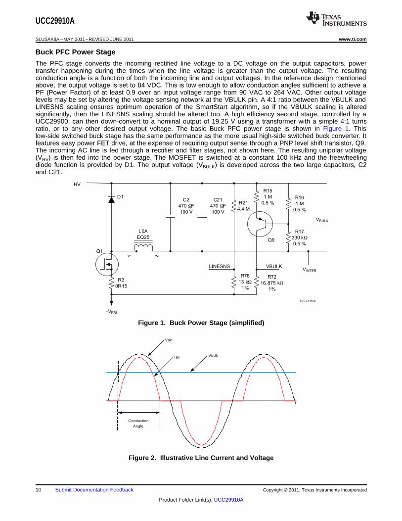
Buck PFC Power Stage
The PFC stage converts the incoming rectified line voltage to a DC voltage on the output capacitors, powertransfer happening during the times when the line voltage is greater than the output voltage. The resultingconduction angle is a function of both the incoming line and output voltages. In the reference design mentionedabove, the output voltage is set to 84 VDC. This is low enough to allow conduction angles sufficient to achieve aPF (Power Factor) of at least 0.9 over an input voltage range from 90 VAC to 264 VAC. Other output voltagelevels may be set by altering the voltage sensing network at the VBULK pin. A 4:1 ratio between the VBULK andLINESNS scaling ensures optimum operation of the SmartStart algorithm, so if the VBULK scaling is alteredsignificantly, then the LINESNS scaling should be altered too. A high efficiency second stage, controlled by aUCC29900, can then down-convert to a nominal output of 19.25 V using a transformer with a simple 4:1 turnsratio, or to any other desired output voltage. The basic Buck PFC power stage is shown in Figure 1. Thislow-side switched buck stage has the same performance as the more usual high-side switched buck converter. Itfeatures easy power FET drive, at the expense of requiring output sense through a PNP level shift transistor, Q9.The incoming AC line is fed through a rectifier and filter stages, not shown here. The resulting unipolar voltage(VHV) is then fed into the power stage. The MOSFET is switched at a constant 100 kHz and the freewheelingdiode function is provided by D1. The output voltage (VBULK) is developed across the two large capacitors, C2and C21.
Figure 1. Buck Power Stage (simplified)
Figure 2. Illustrative Line Current and Voltage
10 Submit Documentation Feedback Copyright © 2011, Texas Instruments Incorporated
Product Folder Link(s): UCC29910A

UCC29910A
www.ti.com SLUSAK8A –MAY 2011–REVISED JUNE 2011
The buck converter operates off a rectified sinusoid and there are periodic dead times when the input voltage islower than the output. During these times no power can be transferred to the output and the input current isnominally zero. Figure 2 shows the line current, IAC, falling to zero when VAC is less than VBULK. The associatedconduction angle increases as the RMS line voltage increases and the current waveform changes from low lineto high line. The input current is skewed a little towards the beginning of the conduction cycle because VBULK isat its lowest value at this time so conduction starts at a lower voltage than it finishes. This effect may be seen inFigure 3 and Figure 4. These waveforms are taken from a 90-W buck PFC reference design, both meet theharmonics requirements set out in EN61000-3-2 and their PF is greater than 90%.
Figure 3. 115 V, 60 Hz, Full Load, 0.5 A/div
Figure 4. 230 V, 50 Hz, Full Load, 0.5 A/div
Copyright © 2011, Texas Instruments Incorporated Submit Documentation Feedback 11
Product Folder Link(s): UCC29910A

10 1 11 13
9
2
5
4
3
8
6
12147
TST VDD NC PFCDRV
VBULK
CS
LINESNS
CSBIAS
CTRLVSSNC
BIASSNS
FAULT
REFIN
R86
300 kW
C80
100 nFTP4
C78
470 nF
R75
143 kW
5%
U13
TLVH431ACDBZR
R76
30 kW
5%
R76
14.3 kW
4
2
5
GND
VIN OUT
U10
TPS71533DCKR
U1
UCC29910APW
R77
1 M
R80
390 W
R5
10 kW
R85
56 kW
R84
680 kW
C45
100 mF
16 V
HV
VPRI
VCCA VDD_3V
Q12
BSS126
UDG-11108
UCC29910A
SLUSAK8A –MAY 2011–REVISED JUNE 2011 www.ti.com
Start-Up With External FET
Conventional start-up schemes utilising either resistive or enhancement mode MOSFET feeds incur linedependant static power losses. To avoid these power losses and to obtain an optimum turn-on time an externaldepletion mode FET may be used Figure 5 and Figure 6. The VHV node is connected to the rectified incomingline. Q12 is a depletion mode FET which will start charging C45 as soon as line power is connected. Initially U1is inactive and BIASCTRL is low. The VDD_3V rail will begin to increase as U10 starts to conduct. The POR(Power On Reset) sequence of U1 will begin once this rail gets to about 1.7 V and will execute while theVDD_3V rail is being established. The BIASCTRL pin will go high when BIASSNS reaches the VB(max) level. IfVLINESNS is then > VBH, U1 begins to pulse the PFCDRV pin, which starts the process of charging the bulkcapacitors at the output of the buck PFC power stage. The PFCDRV current is drawn from C45, which starts todischarge. If the voltage at the BIASSNS pin falls below VB(min) then PFC switching is disabled and Q12 is turnedon to re-charge C45. With the given component values the VB(max) level corresponds to 12 V and a VB(min) level of6 V at the VCCA rail. The user sets the VB(max) and VB(min) levels depending on the characteristics of anyalternative components used by adjusting R84.
Figure 5. Simplified Schematic
12 Submit Documentation Feedback Copyright © 2011, Texas Instruments Incorporated
Product Folder Link(s): UCC29910A

UCC29910A
www.ti.com SLUSAK8A –MAY 2011–REVISED JUNE 2011
Figure 6. Start-Up Sequence Waveforms (Ch1 (Y), PFCDRV, Ch2 (R), VCCA, Ch3 (B), DUT VO)
Copyright © 2011, Texas Instruments Incorporated Submit Documentation Feedback 13
Product Folder Link(s): UCC29910A

UCC29910A
SLUSAK8A –MAY 2011–REVISED JUNE 2011 www.ti.com
SmartStart, VBULK Ramp-Up
Once VCCA has reached 12 V and Q12 has been turned off, and VLINESNS > VBH, the PFCDRV output of U1becomes active and begins driving the main power MOSFET. The SmartStart algorithm increases VBULK, thevoltage across C2 and C21, as rapidly as possible. This is done by transferring the maximum amount of energypossible during each pulse set. The UCC29910A requires that the inductor has a Volt-sec product withstandrating of 600 Vµs. In fact any inductor suitable for application in a buck PFC stage will already meet thisrequirement in order to carry the full-load currents involved without saturating, therefore the Volt-sec rating willnot result in any additional constraints on the inductor design. However it is more convenient to think in terms ofapplied Volt-sec product rather than the peak-inductor current.
The UCC29910A’s SmartStart algorithm generates a series of pulses for the switching MOSFET which apply aconstant Volt-sec product to the inductor during the on and off intervals. This ensures that the inductor current isramped up as high as possible while the MOSFET is on and then decays to zero during the off time. In fact, TOFFis extended to 110% of nominal which provides margin to ensure the inductor current ramps back to zero. TheUCC29910A measures the instantaneous line voltage and the output voltage (VHV and VBULK in Figure 1). Thevoltage applied to the inductor when Q1 is on is then found by subtracting these two values. It then calculates anappropriate TON corresponding to a 600 V x µs product. TOFF is calculated in a similar fashion except that theinductor voltage during the off time is the voltage on the capacitors C2 and C21 (VBULK) plus the forward voltagedrop in D1 which is assumed to be 0.6 V. Inductor current is controlled on a cycle-by-cycle basis by constrainingthe TON and TOFF values so that the inductor Volt-sec product is never exceeded. The initial TOFF intervals aretypically 1.1 ms long because the bulk capacitor voltage is still very low. As VBULK increases, the currentramp-down rate increases so that the required TOFF reduces, allowing the pulses to occur more frequently. Inaddition, as VBULK rises, the voltage across the PFC inductor during TON will drop, so the on-time is adjusted tomaintain a constant PFC inductor volt-secs product.
During ramp-up the UCC29910A monitors the voltage at the BIASSNS pin and if it falls below VB(MIN) theramp-up operation is terminated and the BIASCTRL pin goes low. In the reference design the minimum biasvoltage will be approximately 6 V. When BIASCTRL goes low, Q12 is turned on again and C45 will begincharging back up towards 12 V. The ramp-up phase is then re-started. A maximum of 10 such restarts is allowedbefore the UCC29910A goes into a latched shutdown mode. Line power cycling is necessary for recovery fromthis mode.
Typically, the capacitor voltage increases monotonically until the voltage at the VBULK pin reaches 1.024 V. Thisis slightly lower than VNM and in the circuit of Figure 1 corresponds to a VBULK across C2 and C21 of 82 V. TheUCC29910A then switches to Normal Mode operation. This approach allows the fastest possible start-up time.
In order to save standby power at no load, once the start-up phase is complete, and VBULK is being regulated(either by the normal mode voltage regulation loop, or the SmartBurst light-load mode), the BIASCTRL pin isdriven high. This turns the start-up fet off which eliminates the power loss in the start-up current path. While inSmartBurst mode the voltage at the BIASSNS input is monitored. If the voltage at this pin drops below VB(min)then the start-up fet is turned back on to recharge the capacitors on the VCCA rail. In this way and with thecomponent values shown, the VCCA rail is maintained above 6 V.
14 Submit Documentation Feedback Copyright © 2011, Texas Instruments Incorporated
Product Folder Link(s): UCC29910A

UCC29910A
www.ti.com SLUSAK8A –MAY 2011–REVISED JUNE 2011
Normal Mode Operation
In normal mode, the VBULK pin is controlled at VNM. Due to the slow voltage loop, and low gain at 100/120 Hz,the voltage loop PI error amp output will be essentially a fixed demand. If the power stage stays in DiscontinuousConduction Mode (DCM) throughout the half-cycle, then peak current will be proportional to (VHV-VBULK) over thehalf cycle and IAVG is approximately proportional to IPEAK. If the power stage transitions into ContinuousConduction Mode (CCM) during the line cycle, the current loop, responding to the average current, keeps thepeak current flatter, so the line current doesn’t quite follow (VIN-VO) anymore but average line current is approxproportional to (VHV-VBULK) over the half-cycle. The overall effect is shown in the current waveforms in Figure 3and Figure 4.
The line voltage is used by the control loop to set dynamic DMIN and DMAX values.
Transient Response and VBULK Regulation
When the UCC29910A is regulating in normal mode, the VBULK pin will be at VNM. An AC ripple at twice linefrequency will be superimposed on this as the PFC stage drives current into the bulk capacitors. The amplitudeof this ripple will be a function of line frequency, capacitance value and load current. Due to the necessary lowcontrol loop bandwidth VBULK will reduce in response to a step load increase. If the load step is large enough tocause the VBULK pin to reduce to less than 0.992 V the loop response is temporarily speeded up until this voltagehas been increased back up to 1.043 V at which point the original loop response is restored.
SmartBurst Mode (light load)
As load current reduces the UCC29910A will continue to regulate the voltage at the VBULK pin at VNM. It will dothis by reducing the PWMDRV waveform duty cycle, except that any pulses which are commanded to be lessthan DMIN will be masked and not delivered to the PWMDRV output. The proportion of cycles thus dropped iscounted over a 10-ms window and if it exceeds 10% the UCC29910A changes its operating mode to SmartBurstmode.
In SmartBurst mode the UCC29910A enters a low power consumption mode to minimize wasted power andimprove light-load efficiency. Every 1 ms (approximately) it samples the voltages at the LINESNS and VBULKpins. If the voltage at VBULK is still within a target window of 1.087 V to 1.074 V no action is taken. The appliedload will eventually cause the bus voltage to drop below this window and a burst of pulses are then output at thePFCDRV pin. These drive the PFC FET and thereby recharge the PFC bus capacitance. The most efficienttransfer of power is achieved by minimizing the number of switching events, thus minimizing switching and gatedrive losses. The line voltage sample is used to set the maximum safe duty cycle for the PFCDRV pulses whilekeeping the inductor current discontinuous, based on an inductor rating of 600 Vµs. The pulse duty cycle isramped from DMIN to this maximum value. At the end of the burst, the pulse duty cycle is ramped back to DMIN.Ramping the duty cycle in this manner avoids the sudden application of high power pulses to the power trainwhich may cause excessive EMI and unwanted audio noise generation. A full SmartBurst pulse will last for 2ms – including the ramp-up time but excluding the ramp-down time.
The SmartBurst pulse train is terminated if the voltage at the VBULK pin reaches the peak value of the allowedwindow, 1.087 V or if it exceeds 2 ms in length. There is a 5-ms minimum time between the start of successiveSmartBurst pulse trains.
The max burst length and minimum burst repetition interval ensure that as load is increased, at some point theburst rate will become insufficient to maintain VBULK. Once the voltage falls below the normal mode setpoint VNMat the VBULK pin the controller reverts to normal regulation mode.
Copyright © 2011, Texas Instruments Incorporated Submit Documentation Feedback 15
Product Folder Link(s): UCC29910A

( )
2
BULKPFC IN(pk) BULK
SW IN(pk) IN(pk)
V1L V V
2 f I V
æ ö= - ç ÷
ç ÷´ ´è ø
( ) ( ) ( )
IN(avg) STARTIN(pk)
IN(pk)START START START
P 1 sin( )I
1 1 12 Vcos sin
4 2 2
´ p - q= ´
´´ p - ´ q ´ q ´ - ´ q
( )( )
2
PFC 3
1 84 VL 2 160 V 84 V 94.9 H
2 100 10 Hz 1.033 A 2 160 V
æ ö= ´ - = mç ÷
´ ´ ´ ´è ø
UCC29910A
SLUSAK8A –MAY 2011–REVISED JUNE 2011 www.ti.com
PFC Inductor Value
The PFC inductor is designed for an inductance value that ensures DCM operation at high line (i.e. >160 VAC),right up to full-peak load. With an appropriate value of inductance, operation at low line should then result inCCM operation over most of the conduction angle at full load. The inductance required is given by:
(1)
where:
(2)
And π is the stage conversion efficiency, θSTART is the phase angle (in radians) at which conduction starts, wherethe instantaneous line voltage equals the bulk voltage. For a 100-W converter with an 84-VBULK DC output weevaluate the equation at 160 V as follows.
(3)
Compared to the Boost PFC, much smaller values of PFC inductance can typically be used in the buck, becausethe voltage differential that needs to be supported across the inductor is lower. Practical inductance values thathave been used in various designs have ranged from ~150 µH at 50 W, to ~80 µH to 100 µH at 90 W to 130 W.
16 Submit Documentation Feedback Copyright © 2011, Texas Instruments Incorporated
Product Folder Link(s): UCC29910A

LOAD cond _ %
BUS 2
BUS BUS(%) AC
PC
V V 2 f
´ q=
´ D ´ ´
BUS 2
900.57
0.965C 628 F84 0.12 2 50
´
= = m´ ´ ´
( )HOLDUP LOAD
BUS 2 2
BUS(min) BUS(min_ reg)
T 2 PC
V V
´ ´=
-
( )( )BUS 2 2
900.003 2
0.965C 381 F84 0.95 70
´ ´
= = m
´ -
UCC29910A
www.ti.com SLUSAK8A –MAY 2011–REVISED JUNE 2011
Bulk Capacitor Choice
The value of bulk capacitance required is dictated by requirements on the allowable ripple voltage and hold-uptime. In applications where hold-up time is not the main factor, then the capacitors should be sized forapproximately 12% peak-to-peak ripple as follows:
(4)
For a typical 90-W adapter using buck PFC, the required bus capacitance for ±6% maximum ripple at 90 VAC/50Hz (12% total ripple) and at 84 VDC bus, assuming 96.5% efficiency of the second stage, would be:
(5)
where:• PLOAD: load power drawn (usually by the second regulation/isolation stage)• CBUS: bus capacitance• θCOND_%: conduction angle at AC line of interest (as decimal percentage of total cycle, e.g. 50% conduction
angle expressed as 0.5)• fAC: AC line frequency
The capacitance required to achieve a specific hold up time may be calculated as follows:
(6)
For example, in order to achieve 3-ms holdup, with nominal bus voltage of 84 VDC, ±5% maximum bus ripple,and 70-VDC minimum bus regulation level for the second stage, the required bus capacitance would becalculated as follows for a 90-W load, assuming 96.5% second stage efficiency:
(7)
References
1. 2009/10 Power Supply Design Seminar - SEM1900 Topic 4, Power Factor Correction Using the BuckTopology – Efficiency Benefits and Practical Design Considerations
REVISION HISTORY
Changes from Original (May 2011) to Revision A Page
• Added New DESCRIPTION .................................................................................................................................................. 1
• Added an updated description for the TST pin. .................................................................................................................... 4
• Added an updated description for the TST pin. .................................................................................................................... 6
• Changed UCC29910A Functional Block Diagram ................................................................................................................ 6
Copyright © 2011, Texas Instruments Incorporated Submit Documentation Feedback 17
Product Folder Link(s): UCC29910A

PACKAGE OPTION ADDENDUM
www.ti.com 11-Apr-2013
Addendum-Page 1
PACKAGING INFORMATION
Orderable Device Status(1)
Package Type PackageDrawing
Pins PackageQty
Eco Plan(2)
Lead/Ball Finish MSL Peak Temp(3)
Op Temp (°C) Top-Side Markings(4)
Samples
UCC29910APW ACTIVE TSSOP PW 14 90 Green (RoHS& no Sb/Br)
CU NIPDAU Level-1-260C-UNLIM -40 to 85 29910A
UCC29910APWR ACTIVE TSSOP PW 14 2000 Green (RoHS& no Sb/Br)
CU NIPDAU Level-1-260C-UNLIM -40 to 85 29910A
(1) The marketing status values are defined as follows:ACTIVE: Product device recommended for new designs.LIFEBUY: TI has announced that the device will be discontinued, and a lifetime-buy period is in effect.NRND: Not recommended for new designs. Device is in production to support existing customers, but TI does not recommend using this part in a new design.PREVIEW: Device has been announced but is not in production. Samples may or may not be available.OBSOLETE: TI has discontinued the production of the device.
(2) Eco Plan - The planned eco-friendly classification: Pb-Free (RoHS), Pb-Free (RoHS Exempt), or Green (RoHS & no Sb/Br) - please check http://www.ti.com/productcontent for the latest availabilityinformation and additional product content details.TBD: The Pb-Free/Green conversion plan has not been defined.Pb-Free (RoHS): TI's terms "Lead-Free" or "Pb-Free" mean semiconductor products that are compatible with the current RoHS requirements for all 6 substances, including the requirement thatlead not exceed 0.1% by weight in homogeneous materials. Where designed to be soldered at high temperatures, TI Pb-Free products are suitable for use in specified lead-free processes.Pb-Free (RoHS Exempt): This component has a RoHS exemption for either 1) lead-based flip-chip solder bumps used between the die and package, or 2) lead-based die adhesive used betweenthe die and leadframe. The component is otherwise considered Pb-Free (RoHS compatible) as defined above.Green (RoHS & no Sb/Br): TI defines "Green" to mean Pb-Free (RoHS compatible), and free of Bromine (Br) and Antimony (Sb) based flame retardants (Br or Sb do not exceed 0.1% by weightin homogeneous material)
(3) MSL, Peak Temp. -- The Moisture Sensitivity Level rating according to the JEDEC industry standard classifications, and peak solder temperature.
(4) Multiple Top-Side Markings will be inside parentheses. Only one Top-Side Marking contained in parentheses and separated by a "~" will appear on a device. If a line is indented then it is acontinuation of the previous line and the two combined represent the entire Top-Side Marking for that device.
Important Information and Disclaimer:The information provided on this page represents TI's knowledge and belief as of the date that it is provided. TI bases its knowledge and belief on informationprovided by third parties, and makes no representation or warranty as to the accuracy of such information. Efforts are underway to better integrate information from third parties. TI has taken andcontinues to take reasonable steps to provide representative and accurate information but may not have conducted destructive testing or chemical analysis on incoming materials and chemicals.TI and TI suppliers consider certain information to be proprietary, and thus CAS numbers and other limited information may not be available for release.
In no event shall TI's liability arising out of such information exceed the total purchase price of the TI part(s) at issue in this document sold by TI to Customer on an annual basis.

TAPE AND REEL INFORMATION
*All dimensions are nominal
Device PackageType
PackageDrawing
Pins SPQ ReelDiameter
(mm)
ReelWidth
W1 (mm)
A0(mm)
B0(mm)
K0(mm)
P1(mm)
W(mm)
Pin1Quadrant
UCC29910APWR TSSOP PW 14 2000 330.0 12.4 6.9 5.6 1.6 8.0 12.0 Q1
PACKAGE MATERIALS INFORMATION
www.ti.com 14-Jul-2012
Pack Materials-Page 1

*All dimensions are nominal
Device Package Type Package Drawing Pins SPQ Length (mm) Width (mm) Height (mm)
UCC29910APWR TSSOP PW 14 2000 367.0 367.0 35.0
PACKAGE MATERIALS INFORMATION
www.ti.com 14-Jul-2012
Pack Materials-Page 2


IMPORTANT NOTICE
Texas Instruments Incorporated and its subsidiaries (TI) reserve the right to make corrections, enhancements, improvements and otherchanges to its semiconductor products and services per JESD46, latest issue, and to discontinue any product or service per JESD48, latestissue. Buyers should obtain the latest relevant information before placing orders and should verify that such information is current andcomplete. All semiconductor products (also referred to herein as “components”) are sold subject to TI’s terms and conditions of salesupplied at the time of order acknowledgment.TI warrants performance of its components to the specifications applicable at the time of sale, in accordance with the warranty in TI’s termsand conditions of sale of semiconductor products. Testing and other quality control techniques are used to the extent TI deems necessaryto support this warranty. Except where mandated by applicable law, testing of all parameters of each component is not necessarilyperformed.TI assumes no liability for applications assistance or the design of Buyers’ products. Buyers are responsible for their products andapplications using TI components. To minimize the risks associated with Buyers’ products and applications, Buyers should provideadequate design and operating safeguards.TI does not warrant or represent that any license, either express or implied, is granted under any patent right, copyright, mask work right, orother intellectual property right relating to any combination, machine, or process in which TI components or services are used. Informationpublished by TI regarding third-party products or services does not constitute a license to use such products or services or a warranty orendorsement thereof. Use of such information may require a license from a third party under the patents or other intellectual property of thethird party, or a license from TI under the patents or other intellectual property of TI.Reproduction of significant portions of TI information in TI data books or data sheets is permissible only if reproduction is without alterationand is accompanied by all associated warranties, conditions, limitations, and notices. TI is not responsible or liable for such altereddocumentation. Information of third parties may be subject to additional restrictions.Resale of TI components or services with statements different from or beyond the parameters stated by TI for that component or servicevoids all express and any implied warranties for the associated TI component or service and is an unfair and deceptive business practice.TI is not responsible or liable for any such statements.Buyer acknowledges and agrees that it is solely responsible for compliance with all legal, regulatory and safety-related requirementsconcerning its products, and any use of TI components in its applications, notwithstanding any applications-related information or supportthat may be provided by TI. Buyer represents and agrees that it has all the necessary expertise to create and implement safeguards whichanticipate dangerous consequences of failures, monitor failures and their consequences, lessen the likelihood of failures that might causeharm and take appropriate remedial actions. Buyer will fully indemnify TI and its representatives against any damages arising out of the useof any TI components in safety-critical applications.In some cases, TI components may be promoted specifically to facilitate safety-related applications. With such components, TI’s goal is tohelp enable customers to design and create their own end-product solutions that meet applicable functional safety standards andrequirements. Nonetheless, such components are subject to these terms.No TI components are authorized for use in FDA Class III (or similar life-critical medical equipment) unless authorized officers of the partieshave executed a special agreement specifically governing such use.Only those TI components which TI has specifically designated as military grade or “enhanced plastic” are designed and intended for use inmilitary/aerospace applications or environments. Buyer acknowledges and agrees that any military or aerospace use of TI componentswhich have not been so designated is solely at the Buyer's risk, and that Buyer is solely responsible for compliance with all legal andregulatory requirements in connection with such use.TI has specifically designated certain components as meeting ISO/TS16949 requirements, mainly for automotive use. In any case of use ofnon-designated products, TI will not be responsible for any failure to meet ISO/TS16949.
Products ApplicationsAudio www.ti.com/audio Automotive and Transportation www.ti.com/automotiveAmplifiers amplifier.ti.com Communications and Telecom www.ti.com/communicationsData Converters dataconverter.ti.com Computers and Peripherals www.ti.com/computersDLP® Products www.dlp.com Consumer Electronics www.ti.com/consumer-appsDSP dsp.ti.com Energy and Lighting www.ti.com/energyClocks and Timers www.ti.com/clocks Industrial www.ti.com/industrialInterface interface.ti.com Medical www.ti.com/medicalLogic logic.ti.com Security www.ti.com/securityPower Mgmt power.ti.com Space, Avionics and Defense www.ti.com/space-avionics-defenseMicrocontrollers microcontroller.ti.com Video and Imaging www.ti.com/videoRFID www.ti-rfid.comOMAP Applications Processors www.ti.com/omap TI E2E Community e2e.ti.comWireless Connectivity www.ti.com/wirelessconnectivity
Mailing Address: Texas Instruments, Post Office Box 655303, Dallas, Texas 75265Copyright © 2015, Texas Instruments Incorporated