max5112 9-channel, 14-bit, current dac with i2c interface · 2 maxim integrated 9-channel, 14-bit,...
TRANSCRIPT
9-Channel, 14-Bit, Current DAC with I2C Interface
MAX5112
19-6060; Rev 2; 5/13
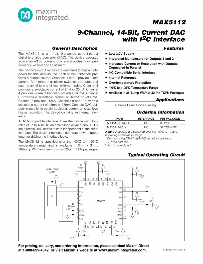
General DescriptionThe MAX5112 is a 14-bit, 9-channel, current-output digital-to-analog converter (DAC). The device operates from a low +3.0V power supply and provides 14-bit per-formance without any adjustment.
The device’s output ranges are optimized to bias a high-power tunable laser source. Each of the 9 channels pro-vides a current source. Channels 1 and 2 provide 10mA current. An internal multiplexer switches the outputs of each channel to one of four external nodes. Channel 3 provides a selectable current of 2mA or 20mA. Channel 4 provides 90mA. Channel 5 provides 180mA. Channel 6 provides a selectable current of -60mA or +300mA. Channel 7 provides 90mA. Channels 8 and 9 provide a selectable current of 15mA or 35mA. Connect DAC out-puts in parallel to obtain additional current or to achieve higher resolution. The device contains an internal refer-ence.
An I2C-compatible interface drives the device with clock rates of up to 400kHz. An active-high asynchronous CLR input resets DAC codes to zero independent of the serial interface. The device provides a separate power-supply input for driving the interface logic.
The MAX5112 is specified over the -40NC to +105NC temperature range, and is available in 3mm x 3mm, 36-bump WLP and 5mm x 5mm, 32-pin TQFN packages.
FeaturesS Low 3.0V Supply
S Integrated Multiplexers for Outputs 1 and 2
S Increased Current or Resolution with Outputs Connected in Parallel
S I2C-Compatible Serial Interface
S Internal Reference
S Overtemperature Protection
S -40NC to +105NC Temperature Range
S Available in 36-Bump WLP or 32-Pin TQFN Packages
ApplicationsTunable Laser Diode Biasing
Ordering Information
Note: All devices are specified over the -40°C to +105°C operating temperature range.+Denotes a lead(Pb)-free/RoHS-compliant package.T = Tape and reel.*EP = Exposed pad.
Typical Operating Circuit
PART INTERFACE PIN-PACKAGE
MAX5112GWX+T I2C 36 WLP
MAX5112GTJ+ I2C 32 TQFN-EP*
MAX5112
1SDA
2SCL
3A0
4A1
5VDDI
6DGND
7AGND
8CLR
9OP
710
V DD1
11OP
812
OP3
13N.C.
14OP
415
V DD2
16OP
1A
24VSS
23VDD5
22OP6
21VDD4
20VDD3
19OP1D
18OP1C
17OP1B
32V D
D731
OP5
30OP
929
V DD6
28OP
2A27
OP2B
26OP
2C25
OP2D
C20.1µF
C10.1µF
C90.1µF
C80.1µF
C70.1µF
C40.1µF
C60.1µF
C50.1µF
µC
C100.1µF
DIGITAL POWERSUPPLY
VDD
VDD
VDD VDD
VSS
C30.1µFVDD
For pricing, delivery, and ordering information, please contact Maxim Direct at 1-888-629-4642, or visit Maxim’s website at www.maximintegrated.com.
2 Maxim Integrated
9-Channel, 14-Bit, Current DAC with I2C Interface
MAX5112
Stresses beyond those listed under “Absolute Maximum Ratings” may cause permanent damage to the device. These are stress ratings only, and functional operation of the device at these or any other conditions beyond those indicated in the operational sections of the specifications is not implied. Exposure to absolute maximum rating conditions for extended periods may affect device reliability.
VDD to AGND .................…………………………..-0.3V to +4.0VVSS to AGND ........................................................-6.0V to +0.3VVDDI to AGND ......................................................-0.3V to +6.0VOP6 to AGND……the higher of (VDD - 9V), (VSS - 0.3V) and -6.0V
to the lower of (VDD + 0.3V) and +4.0VOP1 to OP5 and OP7, OP8, OP9 to AGND ...-0.3V to the lower of (VDD + 0.3V) and +4.0VA1 to DGND .... -0.3V to the lower of (VDDIO + 0.3V) and +6.0VN.C. to AGND ......-0.3V to the lower of (VDD + 0.3V) and +4.0VDigital I/Os to DGND ............................................-0.3V to +6.0VAGND to DGND ...................................................-0.3V to +0.3V
All Other Pins to AGND. ..………………………….-0.3V to +4.0VContinuous Power Dissipation (TA = +70NC) WLP (derate at 26.3mW/NC above +70NC) .................. 2104mW TQFN (derate at 34.5mW/NC above +70NC) ..............2758mWMaximum Current Into Any Pin ........................................380mAOperating Temperature Range ........................ -40NC to +105NCStorage Temperature Range ............................ -65NC to +150NCJunction Temperature .....................................................+150NC Lead Temperature (TQFN only, soldering 10s) ..............+300NCSoldering Temperature (reflow) ......................................+260NC
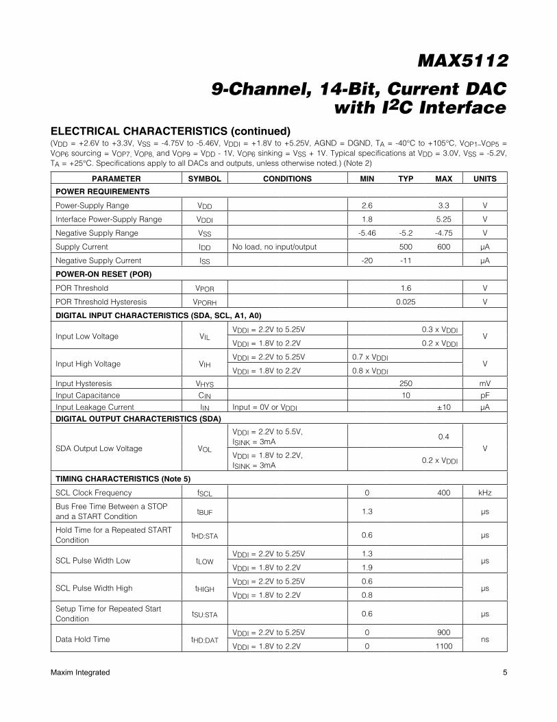
ELECTRICAL CHARACTERISTICS(VDD = +2.6V to +3.3V, VSS = -4.75V to -5.46V, VDDI = +1.8V to +5.25V, AGND = DGND, TA = -40NC to +105NC, VOP1–VOP5 = VOP6 sourcing = VOP7, VOP8, and VOP9 = VDD - 1V, VOP6 sinking = VSS + 1V. Typical specifications at VDD = 3.0V, VSS = -5.2V, TA = +25NC. Specifications apply to all DACs and outputs, unless otherwise noted.) (Note 2)
ABSOLUTE MAXIMUM RATINGS
TQFN Junction-to-Ambient Thermal Resistance (qJA) ..........29NC/W Junction-to-Case Thermal Resistance (qJC) ..............1.7NC/W
WLP Junction-to-Ambient Thermal Resistance (qJA) ..........38NC/W
Note 1: Package thermal resistances were obtained using the method described in JEDEC specification JESD51-7, using a four-layer board. For detailed information on package thermal considerations, refer to www.maximintegrated.com/thermal-tutorial.
Package Thermal Characteristics (Note 1)
PARAMETER SYMBOL CONDITIONS MIN TYP MAX UNITS
STATIC PERFORMANCE
Resolution N 14 Bits
Differential Nonlinearity DNL Guaranteed monotonic Q0.5 Q1.0 LSB
Integral Nonlinearity INLOP1 to OP6 source, OP7, OP8, OP9
Q2 Q8LSB
OP6 sink Q8
Full-Scale Output IMAX
OP1 and OP2 10
mA
OP32mA FS range 2
20mA FS range 20
OP4 90
OP5 180
OP6 current source 300
OP6 current sink -60
OP7 90
OP8 and OP9
15mA FS range 15
35mA FS range 35
3Maxim Integrated
9-Channel, 14-Bit, Current DAC with I2C Interface
MAX5112
ELECTRICAL CHARACTERISTICS (continued)(VDD = +2.6V to +3.3V, VSS = -4.75V to -5.46V, VDDI = +1.8V to +5.25V, AGND = DGND, TA = -40NC to +105NC, VOP1–VOP5 = VOP6 sourcing = VOP7, VOP8, and VOP9 = VDD - 1V, VOP6 sinking = VSS + 1V. Typical specifications at VDD = 3.0V, VSS = -5.2V, TA = +25NC. Specifications apply to all DACs and outputs, unless otherwise noted.) (Note 2)
PARAMETER SYMBOL CONDITIONS MIN TYP MAX UNITS
Offset Error (Note 3) OE
OP1 and OP2 -120 -60 0
FA
OP32mA FS range -24 -12 0
20mA FS range -240 -120 0
OP4 -1080 -540 0
OP5 -2160 -1080 0
OP6 current source -3600 -1800 0
OP6 current sink 0 360 720
OP7 -1080 -540 0
OP8 and OP9
15mA FS range -180 -90 0
35mA FS range -420 -210 0
Offset Error Tempco (Note 4) OETC
OP1 and OP2 Q250
nA/NC
OP32mA FS range Q50
20mA FS range Q500
OP4 Q2250
OP5 Q4500
OP6 current source Q7500
OP6 current sink Q1500
OP7 Q2250
OP8 and OP9
15mA FS range Q375
35mA FS range Q875
Ideal Gain IGAIN IMAX /214 mA/LSB
Gain Error (Note 3) GE
All but OP3, 2mA and OP6 sink Q1.3
%FSOP3, 2mA Q1.5
OP6 sink Q5
Gain Error Tempco (Note 4) GETCAll but OP6 sink Q50
ppm/NCOP6 sink Q15
Output Compliance Range VORAll but OP6 sink VGND VDD - 1
VOP6 sink VSS + 1 VDD
DYNAMIC PERFORMANCE
Output Resistance ROUT
OP1 and OP2 2
MI
OP32mA FS range 10
20mA FS range 1
OP4 0.2
OP5 0.1
OP6 current source 0.06
OP6 current sink 0.04
OP7 0.2
OP8 and OP9
15mA FS range 1.3
35mA FS range 0.56
4 Maxim Integrated
9-Channel, 14-Bit, Current DAC with I2C Interface
MAX5112
ELECTRICAL CHARACTERISTICS (continued)(VDD = +2.6V to +3.3V, VSS = -4.75V to -5.46V, VDDI = +1.8V to +5.25V, AGND = DGND, TA = -40NC to +105NC, VOP1–VOP5 = VOP6 sourcing = VOP7, VOP8, and VOP9 = VDD - 1V, VOP6 sinking = VSS + 1V. Typical specifications at VDD = 3.0V, VSS = -5.2V, TA = +25NC. Specifications apply to all DACs and outputs, unless otherwise noted.) (Note 2)
PARAMETER SYMBOL CONDITIONS MIN TYP MAX UNITS
Current-Output Slew Rate SR
OP1 and OP2 5
mA/Fs
OP32mA FS range 1
20mA FS range 10
OP4 45
OP5 90
OP6 current source 150
OP6 current sink 30
OP7 45
OP8 and OP9
15mA FS range 7.5
35mA FS range 17.5
Output Settling Time tOS tO Q0.1% 15 Fs
Noise at Full Scale (10kHz) INO
OP1 and OP2 1.6
nA/√Hz
OP32mA FS range 0.4
20mA FS range 3.4
OP4 16
OP5 31
OP6 current source 56
OP6 current sink 11
OP7 16
OP8 and OP9
15mA FS range 2.8
35mA FS range 6.5
DAC Glitch ImpulseMajor-Carry Transition
IOGE
OP1 and OP2 60
pC
OP3, 20mA 120
OP4 540
OP5 1080
OP6 current source 1800
OP6 current sink 360
OP7 540
OP8 and OP9
15mA FS range 90
35mA FS range 210
DAC Output GND Switch Resistance
RGSW At 0.7V 50 I
DAC Output GND Switch Current IGSW At 0.7V 14 mA
OVERTEMPERATURE DETECTORS
Overtemperature Disable Threshold TOVTD +160 NC
Overtemperature Warning Threshold
TOVTW +150 NC
5Maxim Integrated
9-Channel, 14-Bit, Current DAC with I2C Interface
MAX5112
ELECTRICAL CHARACTERISTICS (continued)(VDD = +2.6V to +3.3V, VSS = -4.75V to -5.46V, VDDI = +1.8V to +5.25V, AGND = DGND, TA = -40NC to +105NC, VOP1–VOP5 = VOP6 sourcing = VOP7, VOP8, and VOP9 = VDD - 1V, VOP6 sinking = VSS + 1V. Typical specifications at VDD = 3.0V, VSS = -5.2V, TA = +25NC. Specifications apply to all DACs and outputs, unless otherwise noted.) (Note 2)
PARAMETER SYMBOL CONDITIONS MIN TYP MAX UNITS
POWER REQUIREMENTS
Power-Supply Range VDD 2.6 3.3 V
Interface Power-Supply Range VDDI 1.8 5.25 V
Negative Supply Range VSS -5.46 -5.2 -4.75 V
Supply Current IDD No load, no input/output 500 600 FA
Negative Supply Current ISS -20 -11 FA
POWER-ON RESET (POR)
POR Threshold VPOR 1.6 V
POR Threshold Hysteresis VPORH 0.025 V
DIGITAL INPUT CHARACTERISTICS (SDA, SCL, A1, A0)
Input Low Voltage VILVDDI = 2.2V to 5.25V 0.3 x VDDI
VVDDI = 1.8V to 2.2V 0.2 x VDDI
Input High Voltage VIHVDDI = 2.2V to 5.25V 0.7 x VDDI
VVDDI = 1.8V to 2.2V 0.8 x VDDI
Input Hysteresis VHYS 250 mV
Input Capacitance CIN 10 pF
Input Leakage Current IIN Input = 0V or VDDI Q10 FA
DIGITAL OUTPUT CHARACTERISTICS (SDA)
SDA Output Low Voltage VOL
VDDI = 2.2V to 5.5V, ISINK = 3mA
0.4
VVDDI = 1.8V to 2.2V, ISINK = 3mA
0.2 x VDDI
TIMING CHARACTERISTICS (Note 5)
SCL Clock Frequency fSCL 0 400 kHz
Bus Free Time Between a STOP and a START Condition
tBUF 1.3 Fs
Hold Time for a Repeated START Condition
tHD:STA 0.6 Fs
SCL Pulse Width Low tLOWVDDI = 2.2V to 5.25V 1.3
FsVDDI = 1.8V to 2.2V 1.9
SCL Pulse Width High tHIGHVDDI = 2.2V to 5.25V 0.6
FsVDDI = 1.8V to 2.2V 0.8
Setup Time for Repeated Start Condition
tSU:STA 0.6 Fs
Data Hold Time tHD:DATVDDI = 2.2V to 5.25V 0 900
nsVDDI = 1.8V to 2.2V 0 1100
6 Maxim Integrated
9-Channel, 14-Bit, Current DAC with I2C Interface
MAX5112
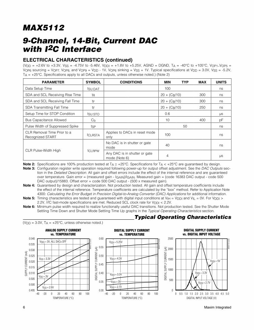
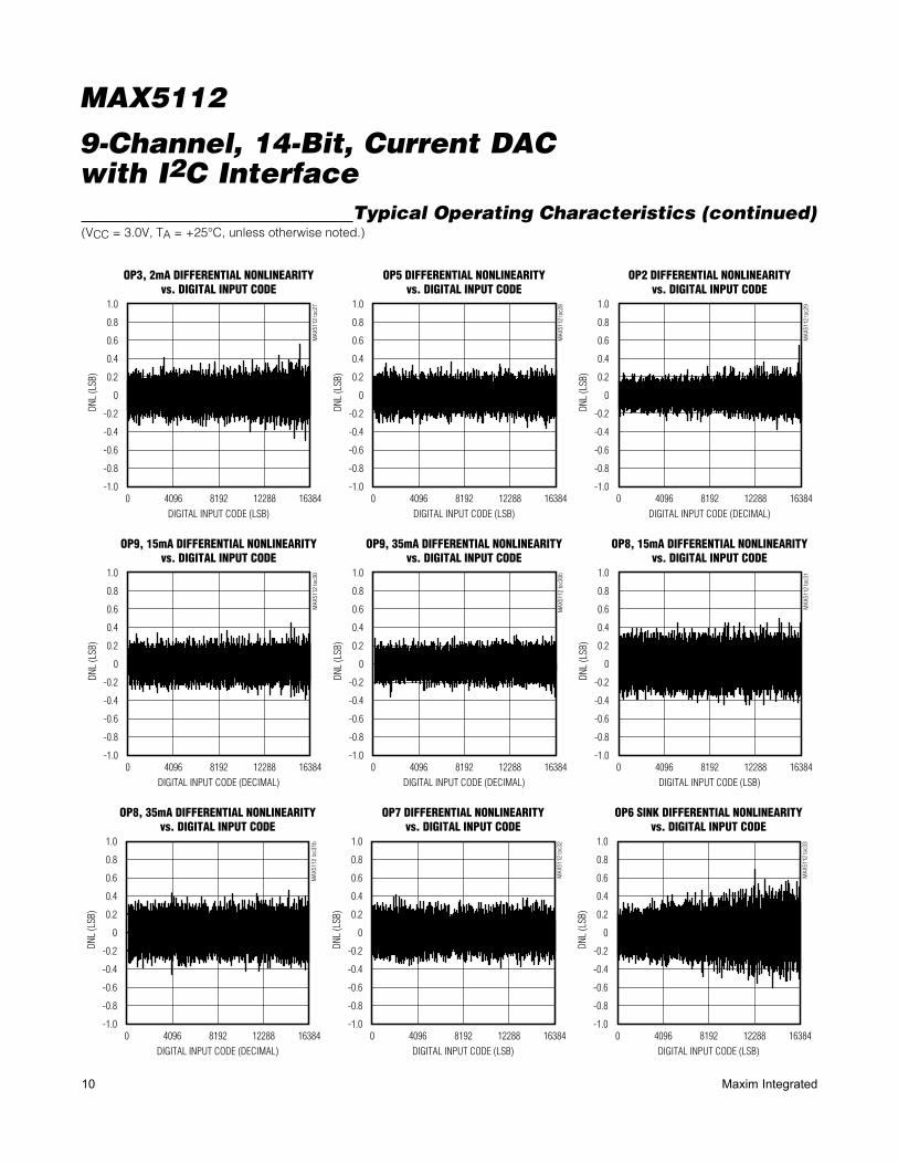
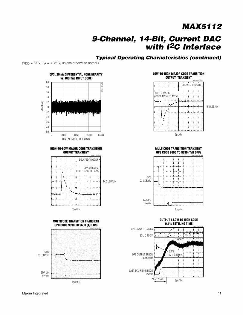
Typical Operating Characteristics(VDD = 3.0V, TA = +25NC, unless otherwise noted.)
ELECTRICAL CHARACTERISTICS (continued)(VDD = +2.6V to +3.3V, VSS = -4.75V to -5.46V, VDDI = +1.8V to +5.25V, AGND = DGND, TA = -40NC to +105NC, VOP1–VOP5 = VOP6 sourcing = VOP7, VOP8, and VOP9 = VDD - 1V, VOP6 sinking = VSS + 1V. Typical specifications at VDD = 3.0V, VSS = -5.2V, TA = +25NC. Specifications apply to all DACs and outputs, unless otherwise noted.) (Note 2)
Note 2: Specifications are 100% production tested at TA ≥ +25NC. Specifications for TA < +25NC are guaranteed by design.Note 3: Configuration register write operation required following power-up for output offset adjustment. See the DAC Outputs sec-
tion in the Detailed Description. All gain and offset errors include the effect of the internal reference and are guaranteed over temperature. Gain error = (measured gain - IGAIN)/IGAIN. Measured gain = (code 16383 DAC output - code 500 DAC output)/15883. Offset error = code 500 DAC output - (500 x measured gain).
Note 4: Guaranteed by design and characterization. Not production tested. All gain and offset temperature coefficients include the effect of the internal reference. Temperature coefficients are calculated by the “box” method. Refer to Application Note 4300: Calculating the Error Budget in Precision Digital-to-Analog Converter (DAC) Applications for additional information.
Note 5: Timing characteristics are tested and guaranteed with digital input conditions at VIH = VDDI and VIL = 0V. For VDDI > 2.2V, I2C fast-mode specifications are met. Reduced SCL clock rate for VDDI < 2.2V.
Note 6: Minimum pulse width required to realize functionally useful DAC transitions. Not production tested. See the Shutter Mode Settling Time Down and Shutter Mode Settling Time Up graphs in the Typical Operating Characteristics section.
PARAMETER SYMBOL CONDITIONS MIN TYP MAX UNITS
Data Setup Time tSU:DAT 100 ns
SDA and SCL Receiving Rise Time tR 20 + (CB/10) 300 ns
SDA and SCL Receiving Fall Time tF 20 + (CB/10) 300 ns
SDA Transmitting Fall Time tF 20 + (CB/10) 250 ns
Setup Time for STOP Condition tSU:STO 0.6 Fs
Bus Capacitance Allowed Cb 10 400 pF
Pulse Width of Suppressed Spike tSP 50 ns
CLR Removal Time Prior to a Recognized START
tCLRSTAApplies to DACs in reset mode only
100 ns
CLR Pulse-Width High tCLRPW
No DAC is in shutter or gate mode
40 ns
Any DAC is in shutter or gate mode (Note 6)
4 Fs
ANALOG SUPPLY CURRENTvs. TEMPERATURE
MAX
5112
toc0
1
TEMPERATURE (°C)
SUPP
LY C
URRE
NT (m
A)
806020 400-20
0.500
0.505
0.510
0.515
0.520
0.525
0.530
0.535
0.540
0.495-40 100
VDDI = 3V, ALL DACs OFF
VDD = 3.3V
VDD = 3V
VDD = 2.6V
DIGITAL SUPPLY CURRENTvs. TEMPERATURE
MAX
5112
toc0
2
TEMPERATURE (°C)
DIGI
TAL
SUPP
LY C
URRE
NT (µ
A)
806040200-20
0.35
0.40
0.45
0.50
0.55
0.60
0.30-40 100
VDDI = 5.25V
VDDI = 4.3V
VDDI = 3.3V
VDDI = 3V
VDDI = 2.7V
DIGITAL SUPPLY CURRENTvs. DIGITAL INPUT VOLTAGE
MAX
5112
toc0
3
DIGI
TAL
SUPP
LY C
URRE
NT (µ
A)
500
1000
1500
2000
2500
0
DIGITAL INPUT VOLTAGE (V)
4.54.03.53.02.52.01.51.00.50 5.0
VDDI = 2.7V
VDDI = 3.3V
VDDI = 5V
7Maxim Integrated
9-Channel, 14-Bit, Current DAC with I2C Interface
MAX5112
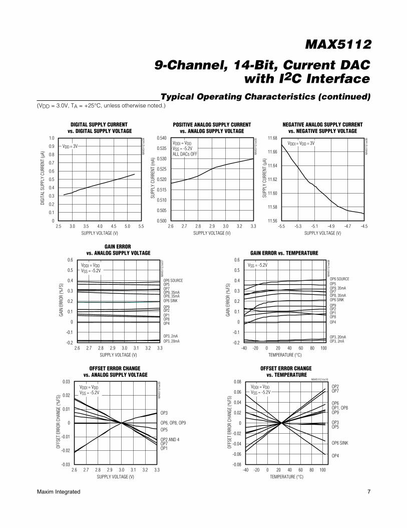
Typical Operating Characteristics (continued)(VDD = 3.0V, TA = +25NC, unless otherwise noted.)
DIGITAL SUPPLY CURRENT vs. DIGITAL SUPPLY VOLTAGE
MAX
5112
toc0
4
SUPPLY VOLTAGE (V)
DIGI
TAL
SUPP
LY C
URRE
NT (µ
A)
5.04.54.03.53.0
0.1
0.2
0.3
0.4
0.5
0.6
0.7
0.8
0.9
1.0
02.5 5.5
VDD = 3V
POSITIVE ANALOG SUPPLY CURRENTvs. ANALOG SUPPLY VOLTAGE
MAX
5112
toc0
5
SUPPLY VOLTAGE (V)
SUPP
LY C
URRE
NT (m
A)
3.22.7 2.8 2.9 3.0
0.505
0.510
0.515
0.520
0.525
0.530
0.535
0.540
0.5002.6 3.3
VDDI = VDDVSS = -5.2VALL DACs OFF
NEGATIVE ANALOG SUPPLY CURRENTvs. NEGATIVE SUPPLY VOLTAGE
MAX
5112
toc0
6
SUPPLY VOLTAGE (V)
SUPP
LY C
URRE
NT (µ
A)
-4.7-4.9-5.1-5.3
11.58
11.60
11.62
11.64
11.66
11.68
11.56-5.5 -4.5
VDDI = VDD = 3V
GAIN ERROR vs. ANALOG SUPPLY VOLTAGE
MAX
5112
toc0
7
SUPPLY VOLTAGE (V)
GAIN
ERR
OR (%
FS)
3.23.12.7 2.8 2.9 3.0
-0.1
0
0.1
0.2
0.3
0.4
0.5
0.6
-0.22.6 3.3
OP6 SOURCEOP5OP7OP9, 35mAOP8, 35mA
OP9
OP1OP2
OP8
OP3, 20mAOP3, 2mA
VDDI = VDDVSS = -5.2V
OP6 SINK
OP4
-40 -20 0 20 40 60 80 100
GAIN ERROR vs. TEMPERATURE
TEMPERATURE (°C)
MAX
5112
toc0
8
GAIN
ERR
OR (%
FS)
-0.1
0.1
0.2
0.3
0.4
0.5
0.6
-0.2
0
VSS = -5.2V
OP5
OP7
OP9OP2OP1OP8OP4
OP3, 20mAOP3, 2mA
OP6 SOURCE
OP6 SINKOP8, 35mA
OP9, 35mA
OFFSET ERROR CHANGE vs. ANALOG SUPPLY VOLTAGE
MAX
5112
toc0
9
SUPPLY VOLTAGE (V)
OFFS
ET E
RROR
CHA
NGE
(%FS
)
3.23.12.7 2.8 2.9 3.02.6 3.3
OP1OP7
OP3
OP5
OP6, OP8, OP9
OP2 AND 4
VDDI = VDDVSS = -5.2V
-0.02
-0.01
0.01
0
0.02
0.03
-0.03
OFFSET ERROR CHANGE vs. TEMPERATURE
MAX5112 toc10
TEMPERATURE (°C)
OFFS
ET E
RROR
CHA
NGE
(%FS
)
100806040200-20
-0.06
-0.02
-0.04
0
0.02
0.04
0.06
0.08
-0.08-40
OP6OP1, OP8OP9
OP3OP5
OP6 SINK
VDDI = VDDVSS = -5.2V
OP4
OP7OP2

8 Maxim Integrated
9-Channel, 14-Bit, Current DAC with I2C Interface
MAX5112
Typical Operating Characteristics (continued)(VDD = 3.0V, TA = +25NC, unless otherwise noted.)
OP9, 15mA INTEGRAL NONLINEARITYvs. DIGITAL INPUT CODE
MAX
5112
toc1
7
DIGITAL INPUT CODE (DECIMAL)
INL
(LSB
)
1228881924096
-6
-4
-2
0
2
4
6
8
-80 16384
OP9, 35mA INTEGRAL NONLINEARITYvs. DIGITAL INPUT CODE
MAX
5112
toc1
7b
DIGITAL INPUT CODE (DECIMAL)
INL
(LSB
)
1228881924096
-6
-4
-2
0
2
4
6
8
-80 16384
OP8, 15mA INTEGRAL NONLINEARITYvs. DIGITAL INPUT CODE
MAX
5112
toc1
8
DIGITAL INPUT CODE (DECIMAL)
INL
(LSB
)
1228881924096
-6
-4
-2
0
2
4
6
8
-80 16384
OP4 INTEGRAL NONLINEARITYvs. DIGITAL INPUT CODE
MAX
5112
toc1
1
DIGITAL INPUT CODE (LSB)
INL
(LSB
)
1228881924096
-6
-4
-2
0
2
4
6
8
-80 16384
OP3, 2mA INTEGRAL NONLINEARITYvs. DIGITAL INPUT CODE
MAX
5112
toc1
2
DIGITAL INPUT CODE (LSB)
INL
(LSB
)
1228881924096
-6
-4
-2
0
2
4
6
8
-80 16384
OP6 INTEGRAL NONLINEARITYvs. DIGITAL INPUT CODE
MAX
5112
toc1
3
DIGITAL INPUT CODE (LSB)
INL
(LSB
)
1228881924096
-6
-4
-2
0
2
4
6
8
-80 16384
OP5 INTEGRAL NONLINEARITYvs. DIGITAL INPUT CODE
MAX
5112
toc1
4
DIGITAL INPUT CODE (LSB)
INL
(LSB
)
1228881924096
-6
-4
-2
0
2
4
6
8
-80 16384
OP1 INTEGRAL NONLINEARITYvs. DIGITAL INPUT CODE
MAX
5112
toc1
5
DIGITAL INPUT CODE (LSB)
INL
(LSB
)
1228881924096
-6
-4
-2
0
2
4
6
8
-80 16384
OP2 INTEGRAL NONLINEARITYvs. DIGITAL INPUT CODE
MAX
5112
toc1
6
DIGITAL INPUT CODE (LSB)
INL
(LSB
)
1228881924096
-6
-4
-2
0
2
4
6
8
-80 16384
9Maxim Integrated
9-Channel, 14-Bit, Current DAC with I2C Interface
MAX5112
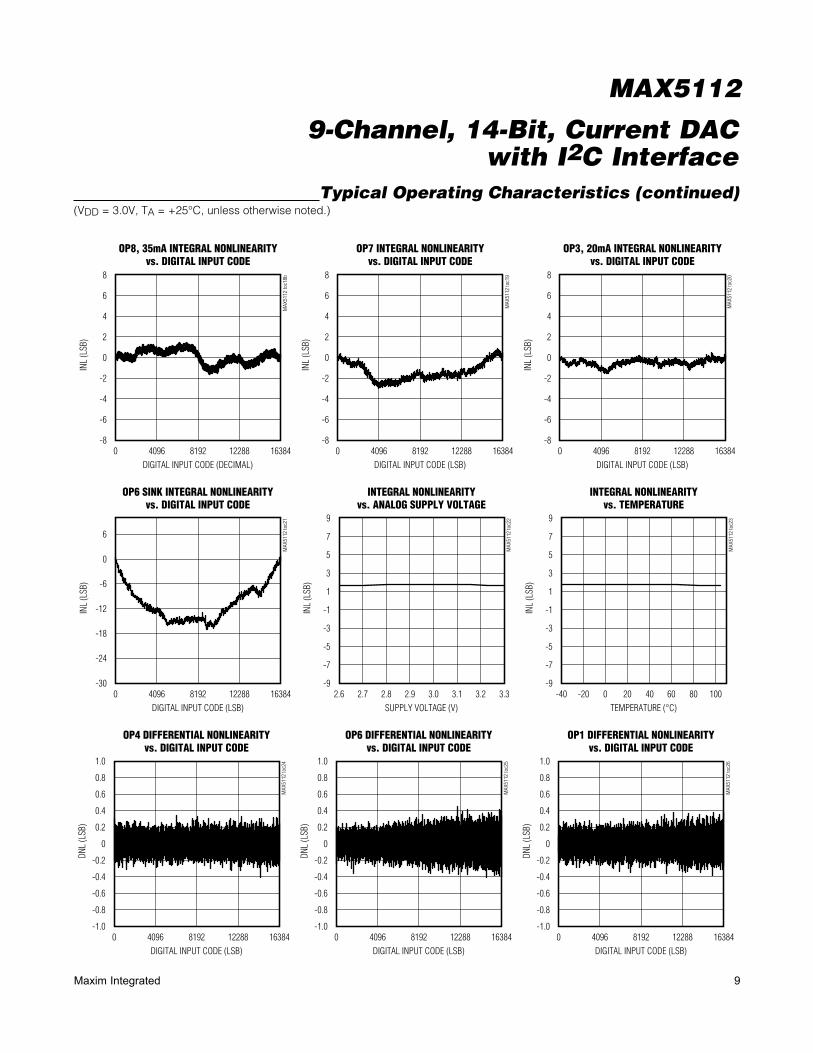
Typical Operating Characteristics (continued)(VDD = 3.0V, TA = +25NC, unless otherwise noted.)
OP8, 35mA INTEGRAL NONLINEARITYvs. DIGITAL INPUT CODE
MAX
5112
toc1
8b
DIGITAL INPUT CODE (DECIMAL)
INL
(LSB
)
1228881924096
-6
-4
-2
0
2
4
6
8
-80 16384
OP7 INTEGRAL NONLINEARITYvs. DIGITAL INPUT CODE
MAX
5112
toc1
9
DIGITAL INPUT CODE (LSB)
INL
(LSB
)
1228881924096
-6
-4
-2
0
2
4
6
8
-80 16384
OP3, 20mA INTEGRAL NONLINEARITYvs. DIGITAL INPUT CODE
MAX
5112
toc2
0
DIGITAL INPUT CODE (LSB)
INL
(LSB
)
1228881924096
-6
-4
-2
0
2
4
6
8
-80 16384
OP6 SINK INTEGRAL NONLINEARITYvs. DIGITAL INPUT CODE
MAX
5112
toc2
1
DIGITAL INPUT CODE (LSB)
INL
(LSB
)
1228881924096
-24
-18
-12
-6
0
6
-300 16384
INTEGRAL NONLINEARITYvs. ANALOG SUPPLY VOLTAGE
MAX
5112
toc2
2
SUPPLY VOLTAGE (V)
INL
(LSB
)
3.23.12.9 3.02.82.7
-7
-5
-3
-1
1
3
5
7
9
-92.6 3.3
INTEGRAL NONLINEARITYvs. TEMPERATURE
MAX
5112
toc2
3
TEMPERATURE (°C)
INL
(LSB
)
806020 400-20
-7
-5
-3
-1
1
3
5
7
9
-9-40 100
OP4 DIFFERENTIAL NONLINEARITYvs. DIGITAL INPUT CODE
MAX
5112
toc2
4
DIGITAL INPUT CODE (LSB)
DNL
(LSB
)
1228881924096
-0.8
-0.6
-0.4
-0.2
0
0.2
0.4
0.6
0.8
1.0
-1.00 16384
OP6 DIFFERENTIAL NONLINEARITYvs. DIGITAL INPUT CODE
MAX
5112
toc2
5
DIGITAL INPUT CODE (LSB)
DNL
(LSB
)
1228881924096
-0.8
-0.6
-0.4
-0.2
0
0.2
0.4
0.6
0.8
1.0
-1.00 16384
OP1 DIFFERENTIAL NONLINEARITYvs. DIGITAL INPUT CODE
MAX
5112
toc2
6
DIGITAL INPUT CODE (LSB)
DNL
(LSB
)
1228881924096
-0.8
-0.6
-0.4
-0.2
0
0.2
0.4
0.6
0.8
1.0
-1.00 16384
10 Maxim Integrated
9-Channel, 14-Bit, Current DAC with I2C Interface
MAX5112
Typical Operating Characteristics (continued)(VCC = 3.0V, TA = +25NC, unless otherwise noted.)
OP8, 35mA DIFFERENTIAL NONLINEARITYvs. DIGITAL INPUT CODE
MAX
5112
toc3
1b
DIGITAL INPUT CODE (DECIMAL)
DNL
(LSB
)
1228881924096
-0.8
-0.6
-0.4
-0.2
0
0.2
0.4
0.6
0.8
1.0
-1.00 16384
OP7 DIFFERENTIAL NONLINEARITYvs. DIGITAL INPUT CODE
MAX
5112
toc3
2
DIGITAL INPUT CODE (LSB)
DNL
(LSB
)
1228881924096
-0.8
-0.6
-0.4
-0.2
0
0.2
0.4
0.6
0.8
1.0
-1.00 16384
OP6 SINK DIFFERENTIAL NONLINEARITYvs. DIGITAL INPUT CODE
MAX
5112
toc3
3
DIGITAL INPUT CODE (LSB)
DNL
(LSB
)
1228881924096
-0.8
-0.6
-0.4
-0.2
0
0.2
0.4
0.6
0.8
1.0
-1.00 16384
OP3, 2mA DIFFERENTIAL NONLINEARITYvs. DIGITAL INPUT CODE
MAX
5112
toc2
7
DIGITAL INPUT CODE (LSB)
DNL
(LSB
)
1228881924096
-0.8
-0.6
-0.4
-0.2
0
0.2
0.4
0.6
0.8
1.0
-1.00 16384
OP9, 15mA DIFFERENTIAL NONLINEARITYvs. DIGITAL INPUT CODE
MAX
5112
toc3
0
DIGITAL INPUT CODE (DECIMAL)
DNL
(LSB
)
1228881924096
-0.8
-0.6
-0.4
-0.2
0
0.2
0.4
0.6
0.8
1.0
-1.00 16384
OP5 DIFFERENTIAL NONLINEARITYvs. DIGITAL INPUT CODE
MAX
5112
toc2
8
DIGITAL INPUT CODE (LSB)
DNL
(LSB
)
1228881924096
-0.8
-0.6
-0.4
-0.2
0
0.2
0.4
0.6
0.8
1.0
-1.00 16384
OP9, 35mA DIFFERENTIAL NONLINEARITYvs. DIGITAL INPUT CODE
MAX
5112
toc3
0b
DIGITAL INPUT CODE (DECIMAL)
DNL
(LSB
)
1228881924096
-0.8
-0.6
-0.4
-0.2
0
0.2
0.4
0.6
0.8
1.0
-1.00 16384
OP2 DIFFERENTIAL NONLINEARITYvs. DIGITAL INPUT CODE
MAX
5112
toc2
9
DIGITAL INPUT CODE (DECIMAL)
DNL
(LSB
)
1228881924096
-0.8
-0.6
-0.4
-0.2
0
0.2
0.4
0.6
0.8
1.0
-1.00 16384
OP8, 15mA DIFFERENTIAL NONLINEARITYvs. DIGITAL INPUT CODE
MAX
5112
toc3
1
DIGITAL INPUT CODE (LSB)
DNL
(LSB
)
1228881924096
-0.8
-0.6
-0.4
-0.2
0
0.2
0.4
0.6
0.8
1.0
-1.00 16384
11Maxim Integrated
9-Channel, 14-Bit, Current DAC with I2C Interface
MAX5112
Typical Operating Characteristics (continued)(VDD = 3.0V, TA = +25NC, unless otherwise noted.)
OP3, 20mA DIFFERENTIAL NONLINEARITYvs. DIGITAL INPUT CODE
MAX
5112
toc3
4
DIGITAL INPUT CODE (LSB)
DNL
(LSB
)
1228881924096
-0.8
-0.6
-0.4
-0.2
0
0.2
0.4
0.6
0.8
1.0
-1.00 16384
HIGH-TO-LOW MAJOR CODE TRANSITIONOUTPUT TRANSIENT
MAX5112 toc36
14.6 LSB/div
2µs/div
OP7, 90mA FS CODE 16256 TO 16255
DELAYED TRIGGER
MULTICODE TRANSITION TRANSIENTOP8 CODE 9690 TO 9630 (T/H ON)
MAX5112 toc36c
OP823 LSB/div
SDA I/O5V/div
2µs/div
LOW-TO-HIGH MAJOR CODE TRANSITIONOUTPUT TRANSIENT
MAX5112 toc35
14.6 LSB/div
2µs/div
OP7, 90mA FS CODE 16255 TO 16256
DELAYED TRIGGER
MULTICODE TRANSITION TRANSIENTOP8 CODE 9690 TO 9630 (T/H OFF)
MAX5112 toc36b
OP823 LSB/div
SDA I/O5V/div
2µs/div
OUTPUT 6 LOW TO HIGH CODE0.1% SETTLING TIME
MAX5112 toc37
2µs/divDt = 12.5µs
OP6, 75mA TO 225mA
SCL, 0 TO 3V
OP6 OUTPUT ERROR0.2mA/div
LAST SCL RISING EDGE2V/div
4µs/div
0.1%DI = 0.225mA
12 Maxim Integrated
9-Channel, 14-Bit, Current DAC with I2C Interface
MAX5112
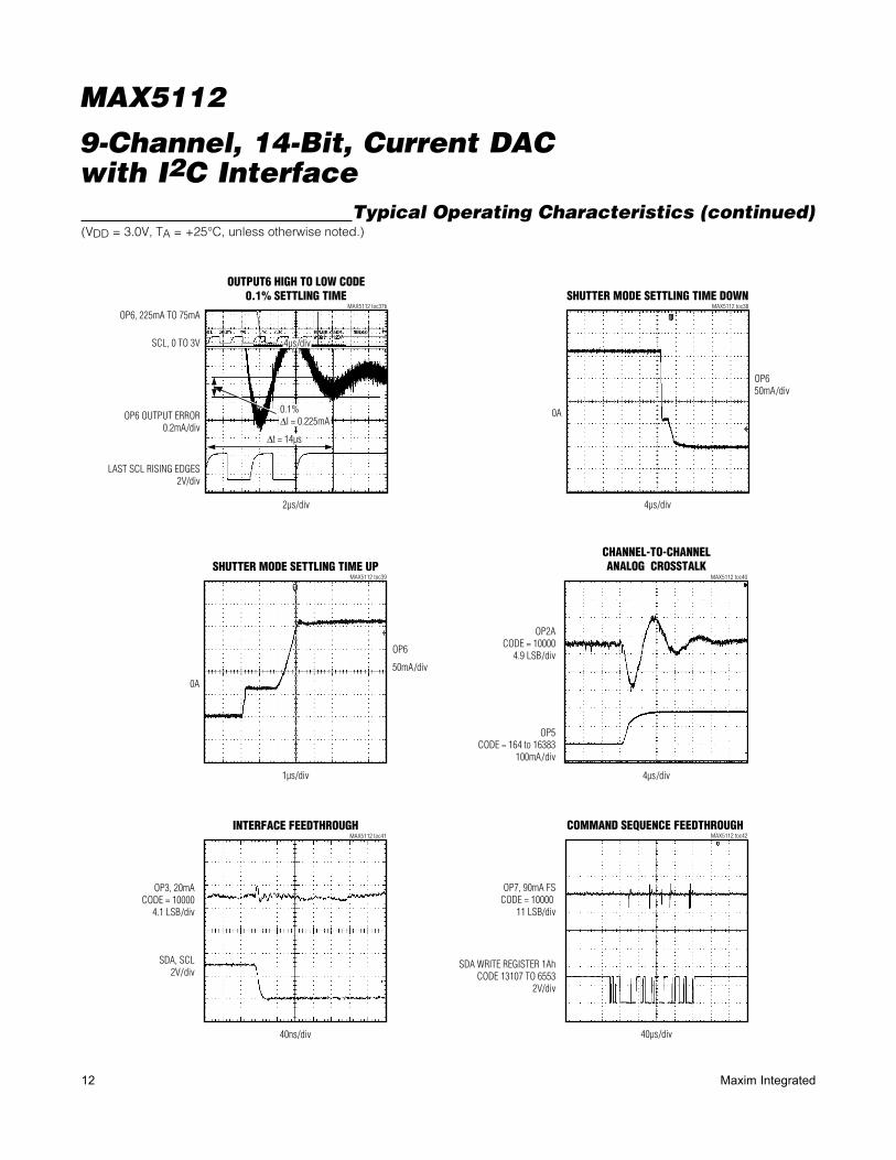
Typical Operating Characteristics (continued)(VDD = 3.0V, TA = +25NC, unless otherwise noted.)
SHUTTER MODE SETTLING TIME UPMAX5112 toc39
OP6
50mA/div
0A
1µs/div
INTERFACE FEEDTHROUGHMAX5112 toc41
40ns/div
OP3, 20mACODE = 10000
4.1 LSB/div
SDA, SCL2V/div
OUTPUT6 HIGH TO LOW CODE0.1% SETTLING TIME
MAX5112 toc37b
2µs/div
OP6, 225mA TO 75mA
SCL, 0 TO 3V
OP6 OUTPUT ERROR0.2mA/div
LAST SCL RISING EDGES2V/div
4µs/div
0.1%DI = 0.225mA
Dt = 14µs
CHANNEL-TO-CHANNELANALOG CROSSTALK
MAX5112 toc40
4µs/div
OP2ACODE = 10000
4.9 LSB/div
OP5CODE = 164 to 16383
100mA/div
COMMAND SEQUENCE FEEDTHROUGH MAX5112 toc42
40µs/div
OP7, 90mA FSCODE = 10000
11 LSB/div
SDA WRITE REGISTER 1AhCODE 13107 TO 6553
2V/div
SHUTTER MODE SETTLING TIME DOWNMAX5112 toc38
OP650mA/div
0A
4µs/div
13Maxim Integrated
9-Channel, 14-Bit, Current DAC with I2C Interface
MAX5112
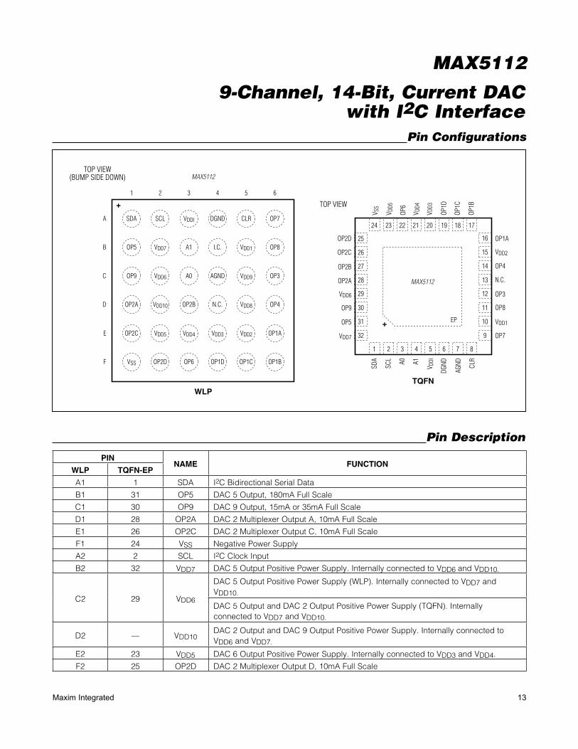
Pin Configurations
Pin Description
TOP VIEW(BUMP SIDE DOWN)
A
B
C
D
WLP
E
F
2 41 5 63
+
+
SDA SCL VDDI DGND CLR OP7
OP5 VDD7 A1 I.C. VDD1 OP8
OP9 VDD6 A0 AGND VDD9 OP3
OP2A VDD10 OP2B N.C. VDD8 OP4
OP2C VDD5 VDD4 VDD3 VDD2 OP1A
VSS OP2D OP6 OP1D OP1C OP1B
MAX5112
MAX5112
TQFN
TOP VIEW
29
30
28
27
12
11
13
SCL A1
V DDI
DGND
AGND
14
SDA
V DD5
V DD4
VDD3
V SS
OP1D
OP1C
1 2
OP2A
4 5 6 7
2324 22 20 19 18
VDD6
OP9
OP4
N.C.
OP3
OP8
A0OP
6
3
21
31 10OP5 VDD1
32 9VDD7
EP
OP7
OP2B
26 15 VDD2OP2C
25 16 OP1A
CLR
OP1B
8
17
OP2D
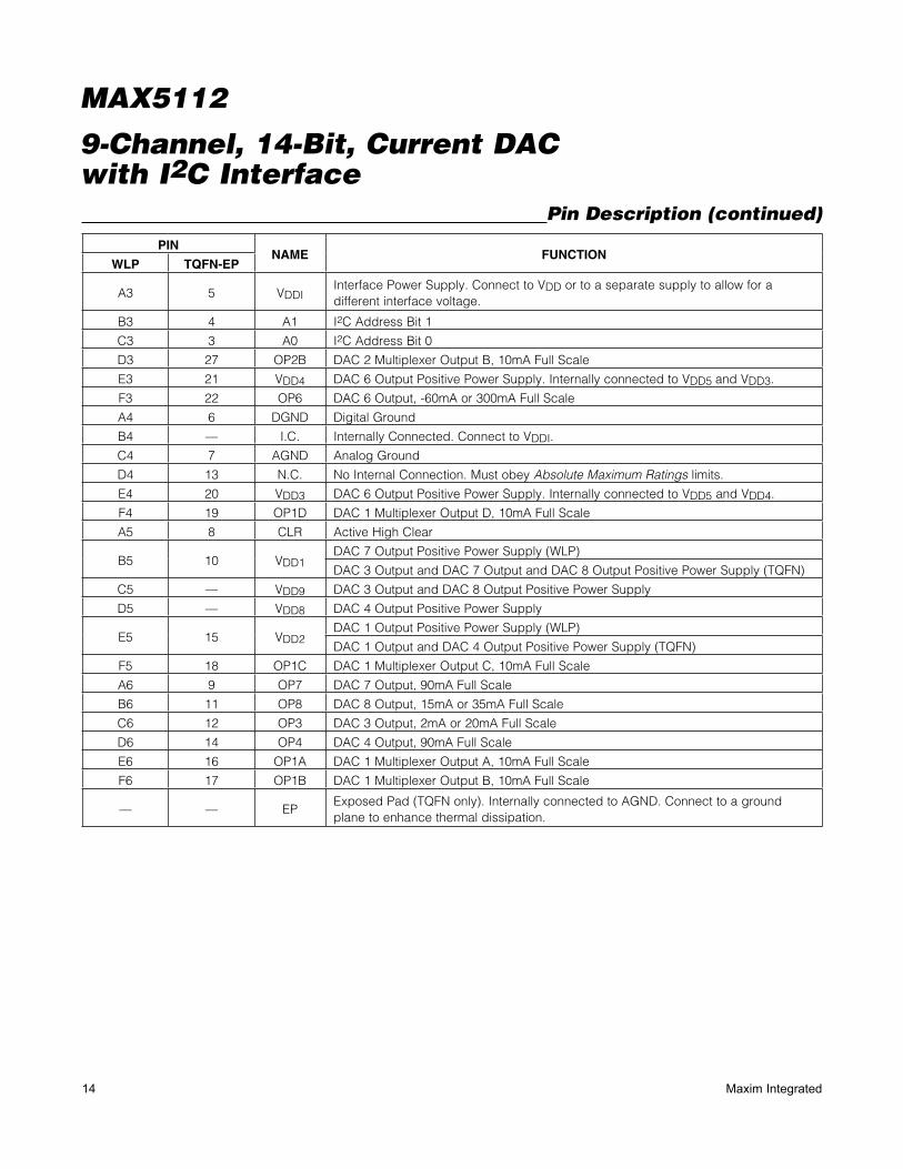
PINNAME FUNCTION
WLP TQFN-EP
A1 1 SDA I2C Bidirectional Serial Data
B1 31 OP5 DAC 5 Output, 180mA Full Scale
C1 30 OP9 DAC 9 Output, 15mA or 35mA Full Scale
D1 28 OP2A DAC 2 Multiplexer Output A, 10mA Full Scale
E1 26 OP2C DAC 2 Multiplexer Output C, 10mA Full Scale
F1 24 VSS Negative Power Supply
A2 2 SCL I2C Clock Input
B2 32 VDD7 DAC 5 Output Positive Power Supply. Internally connected to VDD6 and VDD10.
C2 29 VDD6
DAC 5 Output Positive Power Supply (WLP). Internally connected to VDD7 and VDD10.
DAC 5 Output and DAC 2 Output Positive Power Supply (TQFN). Internally connected to VDD7 and VDD10.
D2 — VDD10DAC 2 Output and DAC 9 Output Positive Power Supply. Internally connected to VDD6 and VDD7.
E2 23 VDD5 DAC 6 Output Positive Power Supply. Internally connected to VDD3 and VDD4.
F2 25 OP2D DAC 2 Multiplexer Output D, 10mA Full Scale
14 Maxim Integrated
9-Channel, 14-Bit, Current DAC with I2C Interface
MAX5112
Pin Description (continued)
PINNAME FUNCTION
WLP TQFN-EP
A3 5 VDDIInterface Power Supply. Connect to VDD or to a separate supply to allow for a different interface voltage.
B3 4 A1 I2C Address Bit 1
C3 3 A0 I2C Address Bit 0
D3 27 OP2B DAC 2 Multiplexer Output B, 10mA Full Scale
E3 21 VDD4 DAC 6 Output Positive Power Supply. Internally connected to VDD5 and VDD3.
F3 22 OP6 DAC 6 Output, -60mA or 300mA Full Scale
A4 6 DGND Digital Ground
B4 — I.C. Internally Connected. Connect to VDDI.
C4 7 AGND Analog Ground
D4 13 N.C. No Internal Connection. Must obey Absolute Maximum Ratings limits.
E4 20 VDD3 DAC 6 Output Positive Power Supply. Internally connected to VDD5 and VDD4.
F4 19 OP1D DAC 1 Multiplexer Output D, 10mA Full Scale
A5 8 CLR Active High Clear
B5 10 VDD1DAC 7 Output Positive Power Supply (WLP)
DAC 3 Output and DAC 7 Output and DAC 8 Output Positive Power Supply (TQFN)
C5 — VDD9 DAC 3 Output and DAC 8 Output Positive Power Supply
D5 — VDD8 DAC 4 Output Positive Power Supply
E5 15 VDD2DAC 1 Output Positive Power Supply (WLP)
DAC 1 Output and DAC 4 Output Positive Power Supply (TQFN)
F5 18 OP1C DAC 1 Multiplexer Output C, 10mA Full Scale
A6 9 OP7 DAC 7 Output, 90mA Full Scale
B6 11 OP8 DAC 8 Output, 15mA or 35mA Full Scale
C6 12 OP3 DAC 3 Output, 2mA or 20mA Full Scale
D6 14 OP4 DAC 4 Output, 90mA Full Scale
E6 16 OP1A DAC 1 Multiplexer Output A, 10mA Full Scale
F6 17 OP1B DAC 1 Multiplexer Output B, 10mA Full Scale
— — EPExposed Pad (TQFN only). Internally connected to AGND. Connect to a ground plane to enhance thermal dissipation.
15Maxim Integrated
9-Channel, 14-Bit, Current DAC with I2C Interface
MAX5112
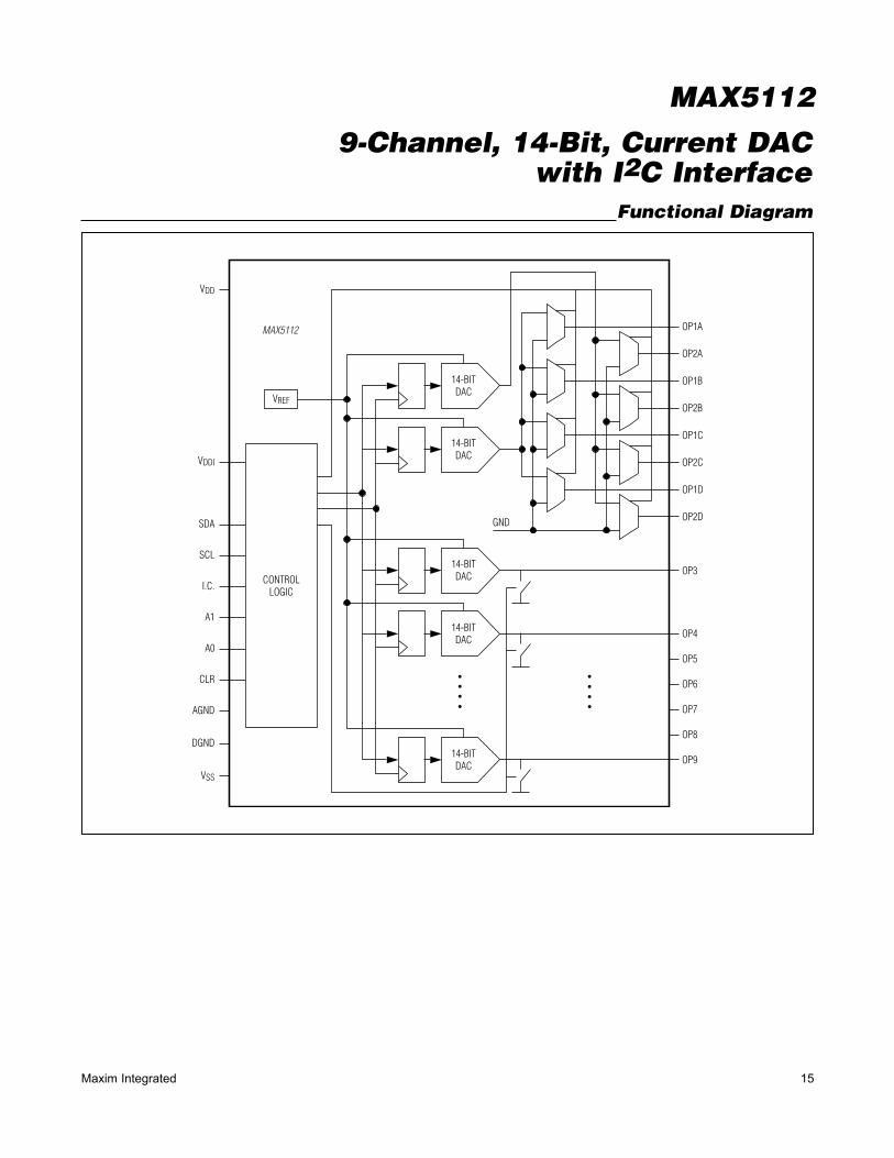
Functional Diagram
14-BITDAC
GNDSDA
SCL
I.C.
A1
A0
CLR
VDDI
VDD
AGND
DGND
VSS
VREF
CONTROLLOGIC
OP4
14-BITDAC
14-BITDAC
14-BITDAC
14-BITDAC
OP1A
OP1B
OP1C
OP1D
OP2A
OP2B
OP2C
OP2D
OP3
OP5
OP6
OP7
OP8
OP9
MAX5112
16 Maxim Integrated
9-Channel, 14-Bit, Current DAC with I2C Interface
MAX5112
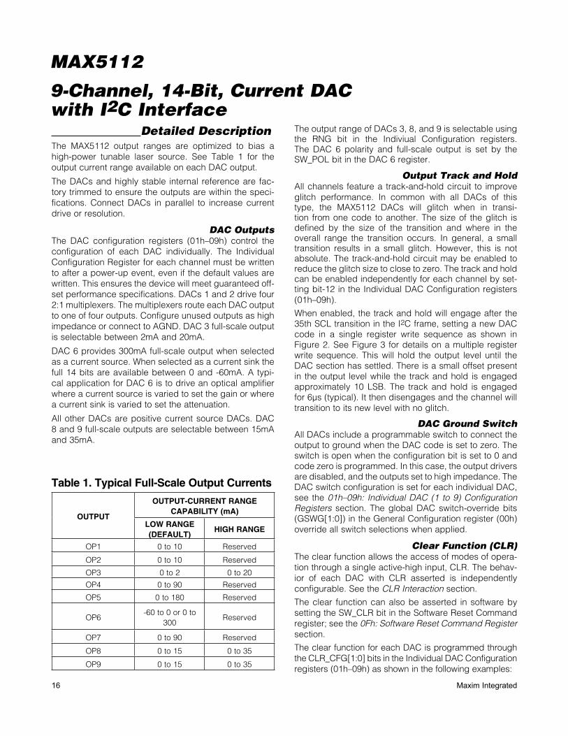
Detailed DescriptionThe MAX5112 output ranges are optimized to bias a high-power tunable laser source. See Table 1 for the output current range available on each DAC output.
The DACs and highly stable internal reference are fac-tory trimmed to ensure the outputs are within the speci-fications. Connect DACs in parallel to increase current drive or resolution.
DAC OutputsThe DAC configuration registers (01h–09h) control the configuration of each DAC individually. The Individual Configuration Register for each channel must be written to after a power-up event, even if the default values are written. This ensures the device will meet guaranteed off-set performance specifications. DACs 1 and 2 drive four 2:1 multiplexers. The multiplexers route each DAC output to one of four outputs. Configure unused outputs as high impedance or connect to AGND. DAC 3 full-scale output is selectable between 2mA and 20mA.
DAC 6 provides 300mA full-scale output when selected as a current source. When selected as a current sink the full 14 bits are available between 0 and -60mA. A typi-cal application for DAC 6 is to drive an optical amplifier where a current source is varied to set the gain or where a current sink is varied to set the attenuation.
All other DACs are positive current source DACs. DAC 8 and 9 full-scale outputs are selectable between 15mA and 35mA.
The output range of DACs 3, 8, and 9 is selectable using the RNG bit in the Indiviual Configuration registers. The DAC 6 polarity and full-scale output is set by the SW_POL bit in the DAC 6 register.
Output Track and HoldAll channels feature a track-and-hold circuit to improve glitch performance. In common with all DACs of this type, the MAX5112 DACs will glitch when in transi-tion from one code to another. The size of the glitch is defined by the size of the transition and where in the overall range the transition occurs. In general, a small transition results in a small glitch. However, this is not absolute. The track-and-hold circuit may be enabled to reduce the glitch size to close to zero. The track and hold can be enabled independently for each channel by set-ting bit-12 in the Individual DAC Configuration registers (01h–09h).
When enabled, the track and hold will engage after the 35th SCL transition in the I2C frame, setting a new DAC code in a single register write sequence as shown in Figure 2. See Figure 3 for details on a multiple register write sequence. This will hold the output level until the DAC section has settled. There is a small offset present in the output level while the track and hold is engaged approximately 10 LSB. The track and hold is engaged for 6µs (typical). It then disengages and the channel will transition to its new level with no glitch.
DAC Ground SwitchAll DACs include a programmable switch to connect the output to ground when the DAC code is set to zero. The switch is open when the configuration bit is set to 0 and code zero is programmed. In this case, the output drivers are disabled, and the outputs set to high impedance. The DAC switch configuration is set for each individual DAC, see the 01h–09h: Individual DAC (1 to 9) Configuration Registers section. The global DAC switch-override bits (GSWG[1:0]) in the General Configuration register (00h) override all switch selections when applied.
Clear Function (CLR)The clear function allows the access of modes of opera-tion through a single active-high input, CLR. The behav-ior of each DAC with CLR asserted is independently configurable. See the CLR Interaction section.
The clear function can also be asserted in software by setting the SW_CLR bit in the Software Reset Command register; see the 0Fh: Software Reset Command Register section.
The clear function for each DAC is programmed through the CLR_CFG[1:0] bits in the Individual DAC Configuration registers (01h–09h) as shown in the following examples:
Table 1. Typical Full-Scale Output Currents
OUTPUT
OUTPUT-CURRENT RANGE CAPABILITY (mA)
LOW RANGE (DEFAULT)
HIGH RANGE
OP1 0 to 10 Reserved
OP2 0 to 10 Reserved
OP3 0 to 2 0 to 20
OP4 0 to 90 Reserved
OP5 0 to 180 Reserved
OP6-60 to 0 or 0 to
300 Reserved
OP7 0 to 90 Reserved
OP8 0 to 15 0 to 35
OP9 0 to 15 0 to 35
17Maxim Integrated
9-Channel, 14-Bit, Current DAC with I2C Interface
MAX5112
• 00 (Ignore): The assertion of CLR does not affect the DAC.
• 01 (Shutter): Shutter mode applies to OP6 only. For all other DACs, shutter mode produces the same effect as ignore. For OP6, the output polarity stays negative for as long as CLR is asserted (level sensitive). The current-sink level is defined by the DAC 6 Shutter Mode Code register (1Bh). Once CLR releases, the DAC out-put returns to the previously programmed value as set in the DAC 6 Source Mode Code register (16h).
• 10 (Gate): The DAC is held at code zero (with ground switches engaged if enabled) as long as CLR is asserted (level sensitive). Once CLR releases, the DAC output returns to the previously programmed value as set in the DAC 1–9 Code register (10h–1Ah).
• 11 (Reset): The DAC is set to code zero (with ground switches engaged if enabled) when CLR is assert-ed and remains at code zero after CLR is released (edge sensitive).
While the clear operation is in effect, DAC channels configured in ignore, shutter, or gate mode continue to accept new code settings. DAC channels configured in reset mode do not accept code changes until the clear operation is terminated.
Software Clear InteractionsThe device provides a software-accessible version of the clear function (SW_CLR), which allows access to the clear functionality directly through the I2C interface (see the 0Fh: Software Reset Command Register sec-tion). When the command 0Fh is used to launch a clear operation, the affected DAC outputs are held in the clear position, determined by the clear configuration settings. This happens from the time when the 0Fh com-mand requesting a clear operation is completed until a second 0Fh command requesting removal of the clear operation is completed. The software- and pin-based clear operations are independently controlled and can be used individually or together without conflict. The devices provide an internal logic-OR circuitry.
Power-On Reset (POR), Power BrownoutThe device contains a POR circuit with a threshold of 1.6V (typ) and a hysteresis of 0.025V (typ). POR ensures that the device resets all registers to default conditions as VDD rises through the upper POR threshold. The default condition of all DAC registers is code zero, with ground switches engaged, ensuring that no large output current transients damage the load during initial power-up.
In a VDD brownout situation, VDD must fall below the lower POR threshold before a POR is issued when VDD rises again. As VDD falls, the device eventually loses
regulation. However, the device is designed to avoid any large output current transients that could damage the load.
Software Reset and Standby FunctionsThe device contains a software reset function. The soft-ware reset function resets all code and configuration registers to default conditions. Write a 1 to the RST bit in the Software Reset Command register (0Fh) to initiate reset. The RST bit is not persistent, so writing a 0 to reset the bit is not required.
The device includes a software standby function that causes all DAC code registers (10h–1Bh) to be set to code zero. Write a 1 to the STDBY bit in the Software Reset Command register (0Fh) to initiate the standby function. The STDBY bit is not persistent, so writing a 0 to reset the bit is not required.
The software standby function is a subset of the software reset function. The software reset function takes effect when both functions are issued.
Overtemperature Error HandlingThe device features an on-chip temperature protection circuit to prevent the device from overheating when all DACs output the maximum programmed current. When the die temperature rises above the threshold tempera-ture, +160NC, the PRO_TEMP bit in the Status/Revision Readback Command register (0Eh) is set and the device enters an overtemperature shutdown mode. All DACs are set to code zero, but the control interface remains active, thereby allowing the host processor to read back the device status. The PRO_TEMP bit is latched and, therefore, the device can only be reset by a software reset command, a software standby command, or by cycling the power.The device features an overtemperature status bit, OVR_TEMP. The OVR_TEMP bit is not latched, and is set if the device temperature is above the protection threshold. The OVR_TEMP bit allows the host processor to determine if the device is too hot to reset. If a software reset is attempt-ed while the device is above the protection threshold, the command is ignored. Similarly, above the threshold die temperature, the device immediately enters shutdown mode when power is cycled.The device features a warning bit, HI_TEMP. The warn-ing bit is not latched and serves as a high-temperature status indicator bit. The HI_TEMP bit is set when the die temperature is typically 10NC below the overtemperature protection threshold.See the Applications Information section for more detail on calculating die temperature and heat-sinking requirements.
18 Maxim Integrated
9-Channel, 14-Bit, Current DAC with I2C Interface
MAX5112
Table 2. User Register/Command Summary
Note: The MAX5112 supports 7-bit command (register) addresses. The 7-bit register address listed above should be left-justified within the I2C command byte. The LSB of the command byte is a don’t-care bit. See Figures 2, 3, and 4 for examples.
User Configuration RegistersTable 2 shows a summary of the register map.
REGISTER ADDRESS (hex)
ACCESS PAIRABLE REGISTER NAME
00h W Y General Configuration
01h W Y DAC 1 Configuration
02h W Y DAC 2 Configuration
03h W Y DAC 3 Configuration
04h W Y DAC 4 Configuration
05h W Y DAC 5 Configuration
06h W Y DAC 6 Configuration
07h W Y DAC 7 Configuration
08h W Y DAC 8 Configuration
09h W Y DAC 9 Configuration
0Ah — — Reserved
0Bh — — Reserved
0Ch — — Reserved
0Dh — — Reserved
0Eh R N Status Feedback and Part ID
0Fh W Y Software Reset/Standby/Clear
10h W Y DAC 1–9 Code
11h W Y DAC 1 Code
12h W Y DAC 2 Code
13h W Y DAC 3 Code
14h W Y DAC 4 Code
15h W Y DAC 5 Code
16h W Y DAC 6 Source Mode Code
17h W Y DAC 7 Code
18h W Y DAC 8 Code
19h W Y DAC 9 Code
1Ah W Y DAC 6 Sink Mode Code
1Bh W Y DAC 6 Shutter Mode Code
1Ch — — Reserved
1Dh — — Reserved
1Eh — — Reserved
1Fh W Y DAC 6 Polarity Control

19Maxim Integrated
9-Channel, 14-Bit, Current DAC with I2C Interface
MAX5112
Register Details00h: General Configuration Register
BIT 15 14 13 12 11 10 9 8
NAME GSWG[1:0] X X X X X X
DEFAULT 0 0 0 0 0 0 0 0
BIT 7 6 5 4 3 2 1 0
NAME X X X X X X X X
DEFAULT 0 0 0 0 0 0 0 0
BIT NAME DESCRIPTION
15:14 GSWG[1:0]
Global GSW Configuration Override00: Individual DAC GSW settings are unaltered01: Individual DAC GSW settings are set to 0 (ground switches disabled)10: Individual DAC GSW settings are set to 1 (ground switches enabled)11: Individual DAC GSW settings are unaltered
13:0 X Reserved
20 Maxim Integrated
9-Channel, 14-Bit, Current DAC with I2C Interface
MAX5112
01h–09h: Individual DAC (1 to 9) Configuration Registers
Note: Any change to individual DAC configuration settings resets the affected DAC code to 0000h.
BIT 15 14 13 12 11 10 9 8
NAME GSW CLR_CFG[1:0] T/H_EN RNG MUX[3:1]
DEFAULT 1 0 0 0 1 1 1 0
BIT 7 6 5 4 3 2 1 0
NAME MUX0 X X X X X X X
DEFAULT 0 0 0 0 0 0 0 0
BIT NAME DESCRIPTION
15 GSW
Ground Switch Control0: Output is left open when DAC code = 0000h1: Output is connected to ground when DAC code = 0000hFor DACs 1 and 2, this setting applies to the active mux output.
14:13 CLR_CFG[1:0]
Clear Configuration Settings (determine how CLR pin affects each DAC)00 (Ignore): The DAC is not affected by the CLR pin (default)01 (Shutter): DAC output polarity is held negative (current level determined by 1Bh) as long as the CLR pin is asserted (level sensitive, applies to DAC 6 only; otherwise, implements the ignore function)10 (Gate): DAC output is held at zero scale (with ground switches engaged if enabled) as long as the CLR pin is asserted (level sensitive)11 (Reset): DAC output is set to zero scale (with ground switches engaged if enabled) when CLR is asserted and remains valid after CLR is removed (edge sensitive)
12 T/H_ENTrack and Hold Enable0: Track and Hold disabled1: Track and Hold enabled
11 RNG
Range (DAC 3, 8, and 9)0: DAC full-scale output level is set to high range.1: DAC full-scale output level is set to low range.Note: For all DACs not suppporting RNG settings, this bit is reserved and should be set to 1 (default).
10:7 MUX[3:0]
Output Mux Settings for DAC (mux settings are only supported for DAC 1 and DAC 2)0000: Output A active, all others high impedance0001: Output B active, all others high impedance0010: Output C active, all others high impedance0011: Output D active, all others high impedance01xx: All outputs high impedance (open)1000: Output A active, all others shunted to GND1001: Output B active, all others shunted to GND1010: Output C active, all others shunted to GND1011: Output D active, all others shunted to GND11xx: All outputs shunted to GND (default)
6:0 X Reserved
21Maxim Integrated
9-Channel, 14-Bit, Current DAC with I2C Interface
MAX5112
0Eh: Status/Revision Readback Command Register
BIT 15 14 13 12 11 10 9 8
NAME PRO_TEMP OVR_TEMP HI_TEMP X PART_ID[3:0]
DEFAULT 0 0 0 0 0 0 0 1
BIT 7 6 5 4 3 2 1 0
NAME REV_ID[3:0] X X X X
DEFAULT 0 1 0 0 0 0 0 0
BIT NAME DESCRIPTION
15 PRO_TEMPOvertemperature Protection Indicator0: Normal operation1: Device overtemperature protection engaged
14 OVR_TEMPOvertemperature Warning Indicator0: Normal operation1: Device temperature is too high (exceeding protection limit)
13 HI_TEMPHigh-Temperature Warning Indicator0: Normal operation1: Device temperature is high (nearing protection limit)
12 X Reserved
11:8 PART_ID[3:0] Part ID Code (0001)
7:4 REV_ID[3:0] Revision Code (0100)
3:0 X Reserved
22 Maxim Integrated
9-Channel, 14-Bit, Current DAC with I2C Interface
MAX5112
Note: A software reset or standby command is required to exit overtemperature-protection mode once engaged (software clear does not qualify for an exit).
0Fh: Software Reset Command Register
10h: Group DAC (1 to 9) Code Command Registers
BIT 15 14 13 12 11 10 9 8
NAME RST STDBY SW_CLR X X X X X
DEFAULT 0 0 0 0 0 0 0 0
BIT 7 6 5 4 3 2 1 0
NAME X X X X X X X X
DEFAULT 0 0 0 0 0 0 0 0
BIT NAME DESCRIPTION
15 RST
Global Reset (identical to a POR)0: No operation1: Reset: All DAC modes, configurations, and codes are returned to their default settingsNot Persistent: The reset operation is contained within the command. It is not necessary to issue a second 0Fh command to remove the reset condition.
14 STDBY
Global Standby (identical to a global power-down)0: No operation1: Standby: All DAC codes are set to zero, but retain all configuration informationNot Persistent: The standby operation is contained within the command. It is not necessary to issue a second 0Fh command to remove the standby condition.Exclusive: If RST and STDBY are requested, STDBY is not issued.
13 SW_CLR
Software Clear0: No operation/remove SW_CLR1: Assert SW_CLRPersistent: The status of SW_CLR remains in effect until changed by a later 0Fh command.Exclusive: If SW_CLR and RST and/or STDBY are requested, SW_CLR is not issued.
12:0 X Reserved
BIT 15 14 13 12 11 10 9 8
NAME B13 B12 B11 B10 B9 B8 B7 B6
DEFAULT 0 0 0 0 0 0 0 0
BIT 7 6 5 4 3 2 1 0
NAME B5 B4 B3 B2 B1 B0 X X
DEFAULT 0 0 0 0 0 0 0 0
BIT NAME DESCRIPTION
15:2 B[13:0]Group DAC Code Setting in Straight Binary Format. All DACs outputs update to code B[13:0] upon command completion.This command is primarily useful for speeding up testing and qualification.
1:0 X Reserved

23Maxim Integrated
9-Channel, 14-Bit, Current DAC with I2C Interface
MAX5112
11h–1Bh: Individual DAC (1 to 9) Code Setting Registers
1Fh: DAC 6 Polarity Command Register
DAC 6 Polarity OperationsSoftware command 1Fh (SW_POL) or the CLR operation in shutter (01) mode controls the polarity of DAC 6. DAC 6 operates in a sink-current mode (0 to -60mA, determined by register 1Ah in sink mode) when SW_POL is set high. When the software command is used, the requested polarity is held in effect from the time when the 1Fh com-mand requesting a polarity change is completed until a second 1Fh command requesting a polarity change operation is completed. When the shutter mode is used, DAC 6 remains in shutter mode as long as CLR is held high. The software- and CLR-driven polarity operations are independently controlled and can be used indi-vidually or together without conflict. The device provides an internal logic-OR operation. Shutter allows the fast
access to a programmable negative code, based on register 1Bh, from either a source or sink mode with a controlled return to the original operating state upon release.
Gate mode is activated by asserting the CLR or through the SW_CLR bit. If gate mode is activated while the DAC is set to sink mode, the DAC remains in sink mode, but the cur-rent is reduced to 0mA for the duration of the gating event.
Similarly, when reset mode is set, the DAC remains in sink mode, but the current is reduced to 0mA and remains there during and after the reset event. All source-, sink-, and shutter-mode current settings are reset to zero by this operation. Shutter mode is inaccessible while DAC 6 is configured for reset.
Note: 11h–19h are DAC code settings for DACs 1–9, respectively. 1Ah is the sink mode code setting for DAC 6. 1Bh is the shutter mode setting for DAC6. See Table 2
BIT 15 14 13 12 11 10 9 8
NAME B13 B12 B11 B10 B9 B8 B7 B6
DEFAULT 0 0 0 0 0 0 0 0
BIT 7 6 5 4 3 2 1 0
NAME B5 B4 B3 B2 B1 B0 X X
DEFAULT 0 0 0 0 0 0 0 0
BIT NAME DESCRIPTION
15:2 B[13:0]DAC Code Settings in Straight Binary Format3FFFh = Full-scale output0000h = Zero-scale output (GSW configuration settings apply)
1:0 X Reserved
BIT 15 14 13 12 11 10 9 8
NAME SW_POL X X X X X X X
DEFAULT 0 0 0 0 0 0 0 0
BIT 7 6 5 4 3 2 1 0
NAME X X X X X X X X
DEFAULT 0 0 0 0 0 0 0 0
BIT NAME DESCRIPTION
15 SW_POLSoftware Polarity Control (to DAC 6 only)0: Source-mode operation (0 to 300mA determined by 16h code, with GSW operation)1: Sink-mode operation (0 to -60mA determined by 1Ah code, GSW operation disabled)
14:0 X Reserved
24 Maxim Integrated
9-Channel, 14-Bit, Current DAC with I2C Interface
MAX5112
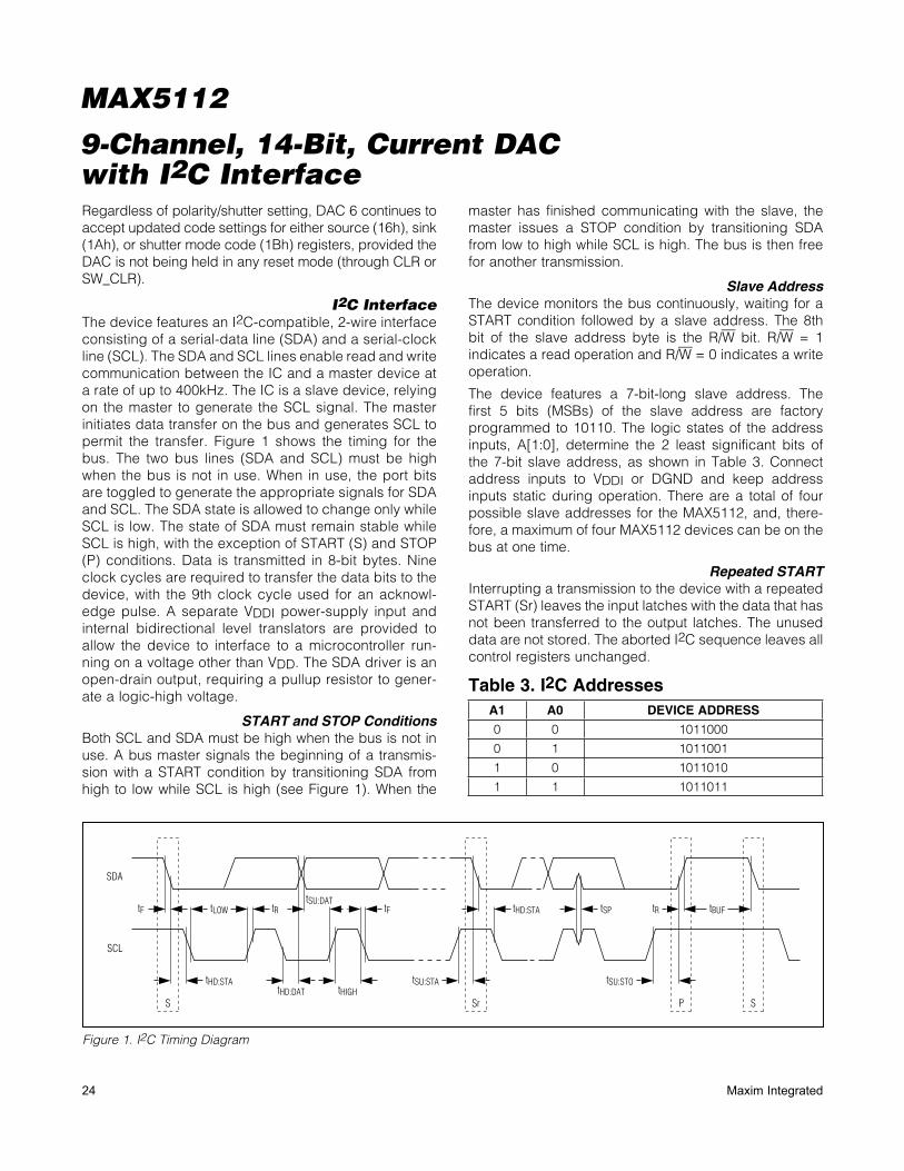
Figure 1. I2C Timing Diagram
Regardless of polarity/shutter setting, DAC 6 continues to accept updated code settings for either source (16h), sink (1Ah), or shutter mode code (1Bh) registers, provided the DAC is not being held in any reset mode (through CLR or SW_CLR).
I2C InterfaceThe device features an I2C-compatible, 2-wire interface consisting of a serial-data line (SDA) and a serial-clock line (SCL). The SDA and SCL lines enable read and write communication between the IC and a master device at a rate of up to 400kHz. The IC is a slave device, relying on the master to generate the SCL signal. The master initiates data transfer on the bus and generates SCL to permit the transfer. Figure 1 shows the timing for the bus. The two bus lines (SDA and SCL) must be high when the bus is not in use. When in use, the port bits are toggled to generate the appropriate signals for SDA and SCL. The SDA state is allowed to change only while SCL is low. The state of SDA must remain stable while SCL is high, with the exception of START (S) and STOP (P) conditions. Data is transmitted in 8-bit bytes. Nine clock cycles are required to transfer the data bits to the device, with the 9th clock cycle used for an acknowl-edge pulse. A separate VDDI power-supply input and internal bidirectional level translators are provided to allow the device to interface to a microcontroller run-ning on a voltage other than VDD. The SDA driver is an open-drain output, requiring a pullup resistor to gener-ate a logic-high voltage.
START and STOP ConditionsBoth SCL and SDA must be high when the bus is not in use. A bus master signals the beginning of a transmis-sion with a START condition by transitioning SDA from high to low while SCL is high (see Figure 1). When the
master has finished communicating with the slave, the master issues a STOP condition by transitioning SDA from low to high while SCL is high. The bus is then free for another transmission.
Slave AddressThe device monitors the bus continuously, waiting for a START condition followed by a slave address. The 8th bit of the slave address byte is the R/W bit. R/W = 1 indicates a read operation and R/W = 0 indicates a write operation.
The device features a 7-bit-long slave address. The first 5 bits (MSBs) of the slave address are factory programmed to 10110. The logic states of the address inputs, A[1:0], determine the 2 least significant bits of the 7-bit slave address, as shown in Table 3. Connect address inputs to VDDI or DGND and keep address inputs static during operation. There are a total of four possible slave addresses for the MAX5112, and, there-fore, a maximum of four MAX5112 devices can be on the bus at one time.
Repeated STARTInterrupting a transmission to the device with a repeated START (Sr) leaves the input latches with the data that has not been transferred to the output latches. The unused data are not stored. The aborted I2C sequence leaves all control registers unchanged.
Table 3. I2C Addresses
SDA
SCL
S Sr SP
tF tF tHD:STA tBUFtSPtR tRtLOWtSU:DAT
tHD:STA tSU:STA tSU:STOtHD:DAT tHIGH
A1 A0 DEVICE ADDRESS
0 0 1011000
0 1 1011001
1 0 1011010
1 1 1011011
25Maxim Integrated
9-Channel, 14-Bit, Current DAC with I2C Interface
MAX5112
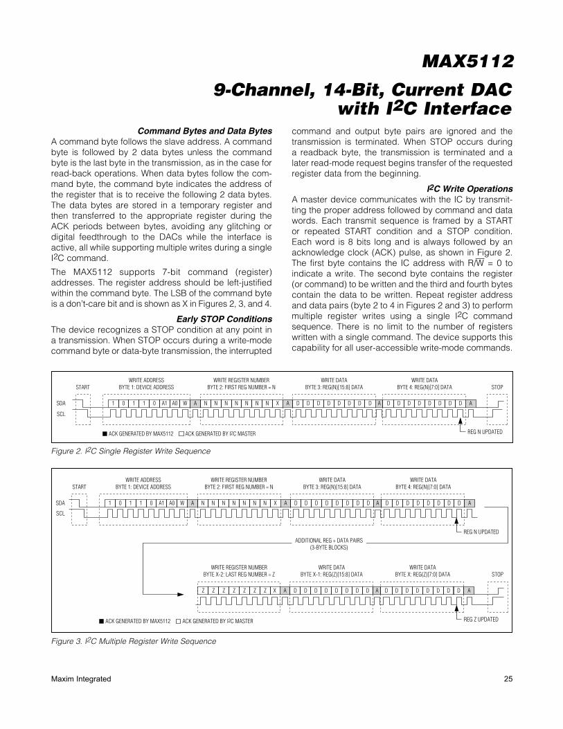
Figure 2. I2C Single Register Write Sequence
Figure 3. I2C Multiple Register Write Sequence
Command Bytes and Data BytesA command byte follows the slave address. A command byte is followed by 2 data bytes unless the command byte is the last byte in the transmission, as in the case for read-back operations. When data bytes follow the com-mand byte, the command byte indicates the address of the register that is to receive the following 2 data bytes. The data bytes are stored in a temporary register and then transferred to the appropriate register during the ACK periods between bytes, avoiding any glitching or digital feedthrough to the DACs while the interface is active, all while supporting multiple writes during a single I2C command.
The MAX5112 supports 7-bit command (register) addresses. The register address should be left-justified within the command byte. The LSB of the command byte is a don’t-care bit and is shown as X in Figures 2, 3, and 4.
Early STOP ConditionsThe device recognizes a STOP condition at any point in a transmission. When STOP occurs during a write-mode command byte or data-byte transmission, the interrupted
command and output byte pairs are ignored and the transmission is terminated. When STOP occurs during a readback byte, the transmission is terminated and a later read-mode request begins transfer of the requested register data from the beginning.
I2C Write OperationsA master device communicates with the IC by transmit-ting the proper address followed by command and data words. Each transmit sequence is framed by a START or repeated START condition and a STOP condition. Each word is 8 bits long and is always followed by an acknowledge clock (ACK) pulse, as shown in Figure 2. The first byte contains the IC address with R/W = 0 to indicate a write. The second byte contains the register (or command) to be written and the third and fourth bytes contain the data to be written. Repeat register address and data pairs (byte 2 to 4 in Figures 2 and 3) to perform multiple register writes using a single I2C command sequence. There is no limit to the number of registers written with a single command. The device supports this capability for all user-accessible write-mode commands.
SCL
START STOP
REG N UPDATED
WRITE ADDRESSBYTE 1: DEVICE ADDRESS
WRITE REGISTER NUMBERBYTE 2: FIRST REG NUMBER = N
WRITE DATABYTE 3: REG(N)[15:8] DATA
WRITE DATABYTE 4: REG(N)[7:0] DATA
SDA 1 0 1 1 0 A1 A0 W A N N N N N N N X A D D D D D D D D A D D D D D D D D A
ACK GENERATED BY MAX5112 ACK GENERATED BY I2C MASTER
SCL
STARTWRITE ADDRESS
BYTE 1: DEVICE ADDRESSWRITE REGISTER NUMBER
BYTE 2: FIRST REG NUMBER = NWRITE DATA
BYTE 3: REG(N)[15:8] DATAWRITE DATA
BYTE 4: REG(N)[7:0] DATA
SDA 1 0 1 1 0 A1 A0 W A N N N N N N N X A D D D D D D D D A D D D D D D D D A
REG N UPDATED
STOPWRITE REGISTER NUMBER
BYTE X-2: LAST REG NUMBER = ZWRITE DATA
BYTE X-1: REG(Z)[15:8] DATAWRITE DATA
BYTE X: REG(Z)[7:0] DATA
Z Z Z Z Z Z Z X A D D D D D D D D A D D D D D D D D A
REG Z UPDATED
ADDITIONAL REG + DATA PAIRS(3-BYTE BLOCKS)
ACK GENERATED BY MAX5112 ACK GENERATED BY I2C MASTER
26 Maxim Integrated
9-Channel, 14-Bit, Current DAC with I2C Interface
MAX5112
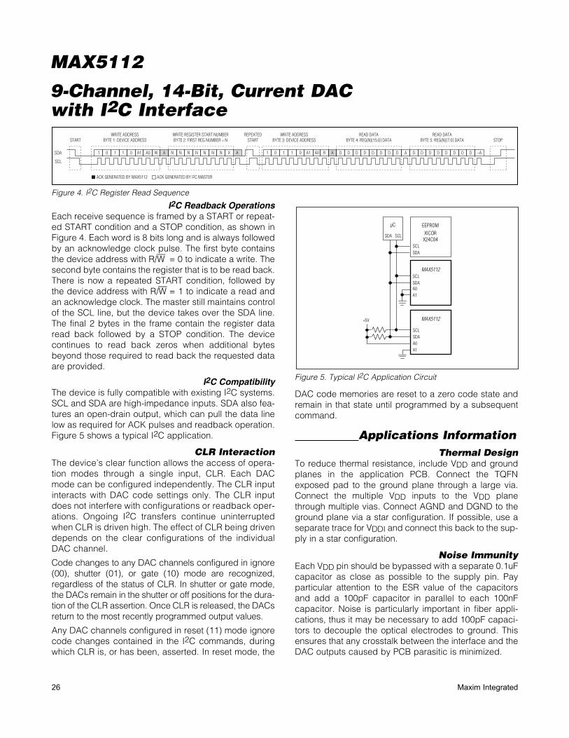
Figure 4. I2C Register Read Sequence
I2C Readback OperationsEach receive sequence is framed by a START or repeat-ed START condition and a STOP condition, as shown in Figure 4. Each word is 8 bits long and is always followed by an acknowledge clock pulse. The first byte contains the device address with R/W = 0 to indicate a write. The second byte contains the register that is to be read back. There is now a repeated START condition, followed by the device address with R/W = 1 to indicate a read and an acknowledge clock. The master still maintains control of the SCL line, but the device takes over the SDA line. The final 2 bytes in the frame contain the register data read back followed by a STOP condition. The device continues to read back zeros when additional bytes beyond those required to read back the requested data are provided.
I2C CompatibilityThe device is fully compatible with existing I2C systems. SCL and SDA are high-impedance inputs. SDA also fea-tures an open-drain output, which can pull the data line low as required for ACK pulses and readback operation. Figure 5 shows a typical I2C application.
CLR InteractionThe device’s clear function allows the access of opera-tion modes through a single input, CLR. Each DAC mode can be configured independently. The CLR input interacts with DAC code settings only. The CLR input does not interfere with configurations or readback oper-ations. Ongoing I2C transfers continue uninterrupted when CLR is driven high. The effect of CLR being driven depends on the clear configurations of the individual DAC channel.
Code changes to any DAC channels configured in ignore (00), shutter (01), or gate (10) mode are recognized, regardless of the status of CLR. In shutter or gate mode, the DACs remain in the shutter or off positions for the dura-tion of the CLR assertion. Once CLR is released, the DACs return to the most recently programmed output values.
Any DAC channels configured in reset (11) mode ignore code changes contained in the I2C commands, during which CLR is, or has been, asserted. In reset mode, the
DAC code memories are reset to a zero code state and remain in that state until programmed by a subsequent command.
Applications InformationThermal Design
To reduce thermal resistance, include VDD and ground planes in the application PCB. Connect the TQFN exposed pad to the ground plane through a large via. Connect the multiple VDD inputs to the VDD plane through multiple vias. Connect AGND and DGND to the ground plane via a star configuration. If possible, use a separate trace for VDDI and connect this back to the sup-ply in a star configuration.
Noise ImmunityEach VDD pin should be bypassed with a separate 0.1uF capacitor as close as possible to the supply pin. Pay particular attention to the ESR value of the capacitors and add a 100pF capacitor in parallel to each 100nF capacitor. Noise is particularly important in fiber appli-cations, thus it may be necessary to add 100pF capaci-tors to decouple the optical electrodes to ground. This ensures that any crosstalk between the interface and the DAC outputs caused by PCB parasitic is minimized.
Figure 5. Typical I2C Application Circuit
START STOPWRITE ADDRESS
BYTE 1: DEVICE ADDRESSWRITE REGISTER START NUMBERBYTE 2: FIRST REG NUMBER = N
REPEATEDSTART
SDA
SCL
1 0 1 1 0 A1 A0 W A A AN N N N N N N X A
READ DATABYTE 4: REG(N)[15:8] DATA
D D D D D D D D
READ DATABYTE 5: REG(N)[7:0] DATA
D D D D D D D D ~A
WRITE ADDRESSBYTE 3: DEVICE ADDRESS
1 0 1 1 0 A1 A0 R
ACK GENERATED BY MAX5112 ACK GENERATED BY I2C MASTER
MAX5112
SDA SCL
µC
SDA
SCL
EEPROM
XICORX24C04
MAX5112
SDA
SCL
A1
A0
SDA
SCL
A1
A0
+5V

27Maxim Integrated
9-Channel, 14-Bit, Current DAC with I2C Interface
MAX5112
Chip InformationPROCESS: BiCMOS
Package InformationFor the latest package outline information and land patterns (foot-prints), go to www.maximintegrated.com/packages. Note that a “+”, “#”, or “-” in the package code indicates RoHS status only. Package drawings may show a different suffix character, but the drawing pertains to the package regardless of RoHS status.
PACKAGE TYPE
PACKAGE CODE
OUTLINE NO.
LAND PATTERN NO.
36 WLP W363A3+1 21-0024Refer to
Application Note 1891
32 TQFN-EP T3255+4 21-0140 90-0012
9-Channel, 14-Bit, Current DAC with I2C Interface
MAX5112
Maxim Integrated cannot assume responsibility for use of any circuitry other than circuitry entirely embodied in a Maxim Integrated product. No circuit patent licenses are implied. Maxim Integrated reserves the right to change the circuitry and specifications without notice at any time. The parametric values (min and max limits) shown in the Electrical Characteristics table are guaranteed. Other parametric values quoted in this data sheet are provided for guidance.
28 Maxim Integrated 160 Rio Robles, San Jose, CA 95134 USA 1-408-601-1000© 2013 Maxim Integrated Products, Inc. Maxim Integrated and the Maxim Integrated logo are trademarks of Maxim Integrated Products, Inc.
Revision History
REVISIONNUMBER
REVISION DATE
DESCRIPTIONPAGES
CHANGED
0 7/12 Initial release —
1 10/12Released the TQFN package and revised the Electrical Characteristics, Typical Operating Circuit, Absolute Maximum Ratings, 01h–09h: Individual DAC (1 to 9) Configuration Registers sections, and Table 1.
1, 2, 4, 16, 20, 26
2 5/13Updated Note 3 in the Electrical Characteristics and revised the DAC Outputs section.
6, 16