materials science copyright © 2020 black phosphorus ...the perovskite-quantum dot (qd) hybrid films...
TRANSCRIPT

Gong et al., Sci. Adv. 2020; 6 : eaay5661 10 April 2020
S C I E N C E A D V A N C E S | R E S E A R C H A R T I C L E
1 of 10
M A T E R I A L S S C I E N C E
Black phosphorus quantum dots in inorganic perovskite thin films for efficient photovoltaic applicationXiu Gong1, Li Guan2, Qingwei Li1*, Yan Li1, Tao Zhang1, Han Pan1, Qiang Sun1, Yan Shen1, Carole Grätzel3, Shaik M. Zakeeruddin3, Michael Grätzel3†, Mingkui Wang1†
Black phosphorus quantum dots (BPQDs) are proposed as effective seed-like sites to modulate the nucleation and growth of CsPbI2Br perovskite crystalline thin layers, allowing an enhanced crystallization and remarkable mor-phological improvement. We reveal that the lone-pair electrons of BPQDs can induce strong binding between molecules of the CsPbI2Br precursor solution and phosphorus atoms stemming from the concomitant reduction in coulombic repulsion. The four-phase transition during the annealing process yields an -phase CsPbI2Br stabilized by BPQDs. The BPQDS/CsPbI2Br core-shell structure concomitantly reinforces a stable CsPbI2Br crystallite and suppresses the oxidation of BPQDs. Consequently, a power conversion efficiency of 15.47% can be achieved for 0.7 wt % BPQDs embedded in CsPbI2Br film-based devices, with an enhanced cell stability, under ambient conditions. Our finding is a decisive step in the exploration of crystallization and phase stability that can lead to the realization of efficient and stable inorganic perovskite solar cells.
INTRODUCTIONUnprecedentedly rapid progress in the field of perovskite solar cells (PSCs) has been achieved in the past few years (1). However, the vulnerability of inorganic-organic hybrid lead perovskite materials to humidity, electrical fields, and light exposure, as well as the intrinsic volatility of organic components such as methylammonium iodide, remains a difficult hurdle to commercialization (2–4). Recently, cesium lead halide CsPbX3 (X = I, Br) inorganic perovskites have been devel-oped as one of the promising alternatives to organic-inorganic hybrid counterparts due to the intrinsic stability coming from the inorganic components (5–7). Although the cubic phase -CsPbI3 has a direct bandgap of 1.73 eV, being suitable for solar cells’ applications, this material suffers from thermodynamic phase instability (8, 9). In a temperature range of 573 to 273 K, the black phase of the -CsPbI3 spontaneously transforms to the undesired yellow -phase (with Eg = 2.82 eV) under open-air ambient (10). The cesium lead dual-halide perovskite CsPbI2Br, formed by partial substitution of the iodide (I) with bromide (Br) to increase tolerance factor (11, 12), is an attractive candidate serving as an absorber layer due to its much more stable phase within a wide temperature range (13–15). A constant energy barrier for ion migration of CsPbI2Br (around 0.45 eV) in the dark and under light illumination further enhances the possibility to attain high photostability (6, 16). However, one of the major challenges for solution-processed CsPbI2Br perovskite thin-film photovoltaics lies in the fabrication of homogenous and pinhole-free large area films. Moreover, some reports have claimed that, compared to the organic- inorganic hybrid counterparts, CsPbI2Br exhibits larger unit cell
volume dependence (17–20), resulting in a smaller diffusion coeffi-cient (0.39 cm2 s−1) (19, 21) and higher defect density and carrier recombination velocity. To achieve high-performance PSCs, it is therefore imperative to fabricate high-quality CsPbI2Br perovskite films with a low defect density and a long carrier diffusion length to accomplish complete carrier extraction (table S1).
To date, introduction of metal ions (K+, Sr2+, Mn2+, etc.) into CsPbI2Br can significantly improve the film quality and charge transport properties (22–24). In addition, a variety of deposition methods including vapor deposition (25), thermal annealing (26), and solvent engineering (27) have been used to control the CsPbI2Br perovskite crystal growth, yielding high-quality films with lower trap densities. The perovskite-quantum dot (QD) hybrid films have attracted no-table attention owing to their unique optoelectronic properties taking advantage of the best individual features of each hybrid component (28–30). For example, PbS and SnS QDs have been successfully incor-porated into organic-inorganic hybrid perovskites films, leading to an improved crystallinity and enhanced carrier diffusion lengths by in-ducing optimal crystal growth and orientation of the perovskite films (28, 30). Black phosphorus QDs (BPQDs), with a size-tunable band-gap, high absorption coefficient, high electron mobility (≈1000 cm2 V−1 s−1) (31, 32), and unique self-repairing properties (33, 34), have been recently incorporated into organic photovoltaics to boost light harvesting (35) and used as a hole/electron transporting material in PSCs to not only enhance charge transport but also induce the forma-tion of high-quality film with favorable textures (36, 37). The compat-ibility of BPQDs to organic-inorganic hybrid halide perovskite has been further demonstrated by using BP as additive into CH3NH3PbI3 precursor solution (38, 39) and thereby improving the quality of pe-rovskite films and augmenting the devices’ power conversion efficiency (PCE) and stability. Recently, Huang et al. (40), using a facile solution- based method, have grown CsPbBr3 nanocrystals directly onto BP sheets, obtaining excellent optical and electronic properties, as well as improved electron transfer capabilities. Moreover, theoretical calcu-lations have indicated a significant potential of inorganic perovskite–BP heterostructures for use in future optoelectronic applications (41, 42). However, thus far, there has not been much effort made toward the
1Wuhan National Laboratory for Optoelectronics, Huazhong University of Science and Technology, Wuhan, Hubei 430074, P.R. China. 2College of Physics Science and Technology, Hebei University, 180 Wusi E Road, Baoding 071000, P.R. China. 3Lab-oratory for Photonics and Interfaces, Swiss Federal Institute of Technology, CH 1015 Lausanne, Switzerland.*Present address: Advanced Research Institute for Multidisciplinary Science, Qilu University of Technology (Shandong Academy of Sciences), Jinan 250353, Shandong, P.R. China.†Corresponding author. Email: [email protected] (M.W.); [email protected] (M.G.)
Copyright © 2020 The Authors, some rights reserved; exclusive licensee American Association for the Advancement of Science. No claim to original U.S. Government Works. Distributed under a Creative Commons Attribution NonCommercial License 4.0 (CC BY-NC).
on May 28, 2020
http://advances.sciencemag.org/
Dow
nloaded from

Gong et al., Sci. Adv. 2020; 6 : eaay5661 10 April 2020
S C I E N C E A D V A N C E S | R E S E A R C H A R T I C L E
2 of 10
exploration of the application of hybrid materials in solar cells, especially not in inorganic perovskite–BP hybrids. A deep under-standing of this hybrid’s physical properties and its full range of ap-plications is still being uncovered.
Here, for the first time, we report significant boosting of carrier transport rate and reduction of defect density in the CsPbI2Br PSCs via hybridization with BPQDs. In this formulation, BPQDs func-tion as effective heterogeneous nucleation sites to promote the for-mation of high-quality and stable CsPbI2Br films. We achieved an impressive PCE of 15.47% with an inverted PSCs’ device based on a CsPbI2Br absorber containing 0.7 weight percent (wt %) BPQDs under AM (air mass) 1.5 G (1 sun illumination).
RESULTSThe BPQDs were synthesized by a facile liquid exfoliation method (43, 44) in a mixed solvent of N,N′-dimethylformamide (DMF) and dimethyl sulfoxide (DMSO) (volume ratio of 9:1). The transmission electron microscopy (TEM) characterization illustrates that the BPQDs obtained are about 3 to 5 nm in diameter with a narrow size distribu-tion (Fig. 1A). The high-resolution TEM (HRTEM) image in Fig. 1B reveals a d-spacing value of 0.26 and 0.17 nm corresponding to the (020) and (060) planes of the BP crystal, respectively. Figure 1C pre-sents the absorption spectra of this solution (15 mg ml−1), showing an absorption in the wavelength region from ultraviolet (UV) to 700 nm. The x-ray photoelectron spectroscopy (XPS) spectrum shows a pre-
dominant P2p peak at around 129.8 eV (Fig. 1D) and O1s peak at 532.1 eV (fig. S1A). The high-resolution P2p spectrum shows doublets at around 130.9 and 129.8 eV, assignable to 2p1/2 and 2p3/2 binding energies, respectively. The O signal is likely to arise from the oxidation of BP, owing to the exposure of the BP sample to the atmosphere during XPS sample preparation.
A uniformly dispersed hybrid precursor solution with varying ra-tios of BPQDs was obtained by dissolving CsPbI2Br and dispersing BPQDs in the same mixed solvent of DMF/DMSO. The facile solution- processed CsPbI2Br crystallization and the reaction compatibility of BPQDs materials provide an opportunity for in situ growth of BPQDs@CsPbI2Br hybrid crystals on solid substrates (40, 44). The top-view scanning electron microscopy (SEM) images were carried out to visualize the morphology of the pristine perovskite films and BPQDs@CsPbI2Br hybrid films consisting of 0.1 to 3 wt % of BPQDs to evaluate their crystallization during the annealing process per-formed at different temperatures. Overall, the samples annealed at 50°C showed continuous and uniform morphology (fig. S2), and the color of film exhibited was black in the corresponding photographs (fig. S3). With increasing temperatures, the perovskite crystals co-alesce to form a large flake crystalline film at 150° to 200°C (brown film) followed by a transformation into large grains at 280°C (black film). We discovered, for the first time, that the crystallization pro-cess of CsPbI2Br thin films involves four phases and three-phase transformations, i.e., fresh film (yellow -phase) at room tempera-ture, black phase at 50°C, brown phase at 150° to 200°C, and black
Fig. 1. Characterization of BPQDs. (A) TEM image. (B) Magnified TEM image (left) and HRTEM image (right) with a scale bar of 2 nm. (C) UV-visible absorption spectroscopy of BPQDs in a solvent mixture of DMF/DMSO (v:v = 9:1). Inset: Photograph of the solution of BPQD (15 mg ml−1). Photo credit Xiu Gong, Huazhong University of Science and Technology. (D) XPS spectroscopy for P 2p of BPQDs.
on May 28, 2020
http://advances.sciencemag.org/
Dow
nloaded from

Gong et al., Sci. Adv. 2020; 6 : eaay5661 10 April 2020
S C I E N C E A D V A N C E S | R E S E A R C H A R T I C L E
3 of 10
cubic -phase at 280°C. It is worth noting that addition of a small amount of BPQDs (0.5 and 0.7 wt %) in the precursor solution sig-nificantly improves the CsPbI2Br films’ morphological properties with regard to surface coverage and surface uniformity (Fig. 2, A to D). We found that the color of BPQDs@CsPbI2Br hybrid films (0.7 wt %) turns from brown to black at 200°C (Fig. 2, E to H). This observa-tion documents that adding BPQDs facilitates the pure -phase for-mation at temperatures lower than 200°C. In situ variable-temperature x-ray diffraction (XRD) characterization was carried out to clarify the phase changes and crystalline processes underway in fabrication of CsPbI2Br films with and without BPQDs (0.7 wt %). In Fig. 2I, the XRD spectrum of CsPbI2Br film at 50°C exhibited two splitting peaks at 14.69° and 29.63° assigned to the (100) and the (200) planes of the perovskite phase, representing low-symmetry tetragonal -phase (45). The XRD spectrum of the film gradually developed into a typ-ical -phase during temperature transitions from 100° to 200°C. After annealing at 280°C, the pure -phase dominated the XRD patterns. These studies further confirm the three-phase transformations, as
discussed earlier, during the crystallization process of CsPbI2Br. In contrast, the XRD spectrum of BPQDs@CsPbI2Br films exhibited the pure -phase characteristic already at 200°C with strong crystal-lization peaks with (100) and (200) orientation during the anneal-ing process (Fig. 2J). These results imply that the BPQDs could lower the energy barrier for formation of the pure -phase perovskite and thus produce smooth and highly crystalline BPQDs@CsPbI2Br films that are conducive to carrier generation and transportation.
The formation of a high-symmetry corner-shared -phase CsPbI2Br crystal occurs via a molecular self-assembly process, thermodynam-ically favored due to a series of [BX6]4− octahedral rotations or tilt-ing to accommodate expansion of the cell volume (46). Therefore, the appearance of a black-phase crystal at 50°C is an indication for the growth of lower-symmetry perovskite-like phases (tetragonal -phase) in the form of CsPbI2Br·DMF·DMSO solvates that result from self- assembly of PbI2, CsBr, and molecular solvents (47, 48). The contin-uous volatilization of solvents with increasing temperatures can induce the collapse of perovskite crystal lattice followed by substantial [BX6]4−
Fig. 2. BPQD-assisted deposition of perovskite films. SEM images of (A to D) CsPbI2Br films and (E to H) BPQDs@CsPbI2Br films consisting of 0.7 wt % of BPQDs an-nealed at a temperature range from 50° to 280°C for 2 min. The insets are the photographs of the corresponding samples. In situ variable-temperature XRD of (I) CsPbI2Br films and (J) BPQDs@CsPbI2Br films consisting of 0.7 wt % of BPQDs. a.u., arbitrary units. Photo credit Xiu Gong, Huazhong University of Science and Technology.
on May 28, 2020
http://advances.sciencemag.org/
Dow
nloaded from

Gong et al., Sci. Adv. 2020; 6 : eaay5661 10 April 2020
S C I E N C E A D V A N C E S | R E S E A R C H A R T I C L E
4 of 10
octahedral rotation or tilting, yielding the -phase (Fig. 2I), that is indicated by a color change of the perovskite films from black to brown (150° to 200°C). Subsequently, enhanced by coulombic force attractions and thermally promoted diffusion, the molecules migrate and the nucleation takes place in the most energetically preferred ori-entation to obtain a pure, highly symmetric, and phase-stable in-organic halide perovskite at 280°C. It is noteworthy that the transition period from black to brown can be reduced via anti-solvent tech-niques that accelerate residual solvent evaporation. This observation has been recently confirmed by Chen et al. (27), who proposed to use the anti-solvent isopropanol, of a low boiling point, to wash away the residual solvents to obtain high-quality CsPbI2Br films. In the present work, the BPQDs are well dispersed within the precursor solution, effectively supplying heterogeneous sites that facilitate the CsPbI2Br nucleation and growth accompanied by solvents’ evaporation as il-lustrated in fig. S4. The introduction of BPQDs substantially shortens the transition period during phase transition and, thus, forms highly pure -phase perovskites at lower temperatures (i.e., 200°C in these experiments). This result was also supported by the uniform large hexagonal grain inlay within the continuous flake crystal surface mor-phology of BPQDs@CsPbI2Br films at 150° to 200°C.
We performed confocal laser scanning fluorescence microscopy (CLSM) to investigate the molecular pathway that follows the in-corporation of small amounts of BPQDs for the modulation of the nucleation and growth of CsPbI2Br perovskite crystalline films. To observe the thin-film nucleation and growth kinetics, the fresh sam-ples were deposited onto nanocrystalline SnO2-coated substrates and
were immediately placed under the CLSM for tracking of the nucle-ation process. With regard to the pristine CsPbI2Br perovskite sam-ples, at the beginning stage (60 s), crystal nuclei with different sizes and shapes start forming on the nanocrystalline SnO2 thin-film surface as shown in Fig. 3A, which can be attributed to a lower nucleation rate compared to crystalline growth rate. Therefore, as temperature increases, these various crystalline nuclei with nonuniform sizes tend to grow into a lump of a larger crystal, resulting in irregularity and voids in the morphology of the perovskite film formed (Fig. 3, B and C). This irregular morphology is shown in Fig. 2D. When using evenly dis-persed BPQDs incorporated into the perovskite precursors, this addi-tive serves to build effective heterogeneous nucleation sites, triggering a uniform growth of CsPbI2Br crystals. Figure 3D shows that due to a high and regular nucleation density, small crystals uniformly disperse over the entire surface of the BPQDs@CsPbI2Br hybrid films. We maintain that the BPQDs can induce the growth of morphologically uniform CsPbI2Br crystals due to diminishing the coulombic repul-sion coming from the lone-pair electrons (LPEs) of phosphorus. The electronic interaction between LPEs and cations of CsPbI2Br might promote the uniform coverage and smooth surface properties of the hybrid films (Fig. 3F). The BPQDs@CsPbI2Br hybrid films exhibit stronger luminescence than the pristine CsPbI2Br films sintered at the same temperature (100°C).
We carried out density functional theory (DFT) calculations on the adhesive energy to further understand the heterogeneous growth of CsPbI2Br molecules onto either the BPQDs or SnO2 substrates, particularly focusing on the adhesive energies for the PbI2 and CsBr
Fig. 3. CLSM characterizations. (A to C) Growth process of CsPbI2Br films as a function of increasing annealing temperatures [CsPbI2Br with perovskite phase, red fluo-rescence (59)] and (D to F) growth process of BPQDs@CsPbI2Br hybrid films consisting of 0.7 wt % BPQDs with augmentation of annealing temperatures [BPQDs, green fluorescence (60)] under excitation by 488- and 543-nm laser beams. Insets show the corresponding confocal microscopy images of the samples under bright field (scale bars, 5 m).
on May 28, 2020
http://advances.sciencemag.org/
Dow
nloaded from

Gong et al., Sci. Adv. 2020; 6 : eaay5661 10 April 2020
S C I E N C E A D V A N C E S | R E S E A R C H A R T I C L E
5 of 10
molecules (Fig. 4). We selected six of the most likely adhesive sites onto the SnO2 nanocrystals (fig. S5) with the goal of establishing an estimation of the corresponding adhesive energies. The results are summarized in table S2. A more negative adhesive energy signifies that there is less of an energy barrier, permitting facile growth of the perovskite crystals onto the substrates. The modeling results indicate that the configurations, PbI2/CsBr and CsBr/PbI2, when attached onto the SnO2 nanocrystals, show the lowest adhesive energies of −0.713 and −1.180 eV, respectively. For comparison, on BPQDs, the adhesive energy decreased substantially to values of −1.218 and −2.084 eV (Fig. 4B), respectively, suggesting that the relatively easy growth of CsPbI2Br crystals on the BPQDs nucleation sites allows the forma-tion of a more stable perovskite film. Moreover, the BPQDs that attached onto SnO2 also exhibited a good stability (adhesive energy being approximately −0.719 eV), indicating that there is also attrac-tion between the BPQDs and SnO2 substrate.
The crystal structure of the BPQDs@CsPbI2Br hybrid film was further analyzed by TEM (fig. S6, A to H). All TEM images were cap-tured at a region distant from the focused beam position because of the vulnerability of the CsPbI2Br perovskite to radiolysis when ex-posed to the 200-keV electron beam (fig. S6D) (49). The TEM images in fig. S6 (B and E) were obtained by adjusting electron-beam focus-ing at BPQDs and beyond dot positions. The distribution of lattice domains shows a clear BPQDS/CsPbI2Br core-shell structure by com-bining HRTEM images in fig. S6 (C and F). As the ratio of BPQD to perovskite decreases, the thickness of perovskite shell onto the BPQD gradually increases until it wraps the core (inset in fig. S6F), and fi-nally forms a continuous matrix with BPQDs embedded inside (fig. S6G). The HRTEM image (fig. S6H) further shows a clear lattice in-terface between perovskite and QDs, indicating good compatibility among the two components. The lattice spacings of 0.29 and 0.26 nm are consistent with the typical (200) and (020) planes of the cubic CsPbI2Br and BPQDs (fig. S6H), respectively, revealing that both CsPbI2Br and BPQDs show good crystallinity within the hybrid struc-ture. Figure S6 (I to N) illustrates the dark-field scanning TEM images
of the BPQDs@CsPbI2Br hybrid films and the corresponding elemen-tal mapping image (Cs, Pb, I, Br, and P), which further confirm the incorporation of P QDs (core) in the CsPbI2Br perovskite shell.
XPS characterization in fig. S7 verifies the chemical states of the fabricated films. Notably, in the BPQDs@CsPbI2Br hybrid films, the peaks for the elements of Cs, Pb, Br, and I are shifted to slightly lower binding energies compared to those in the CsPbI2Br films. The shift to lower binding energy of the hybrid films may be attributed to the strengthening of electron density in CsPbI2Br due to the LPEs of BPQDs. This implies formation of electron donor-acceptor–like bonds via interaction between BPQDs and cations of perovskite. Moreover, Raman spectroscopy confirmed the effect of BPQDs’ LPEs on the BPQDs@CsPbI2Br hybrid. The Raman spectra of the BPQDs@CsPbI2Br hybrid film (fig. S8) exhibit three prominent peaks corre-sponding to one out-of-plane phonon mode A1
g at 361.8 cm−1 and two in-plane modes B2g and A2
g at 438.6 and 464.5 cm−1 of BP, respec-tively. Compared to the bare BPQDs, the A1
g, B2g, and A2g modes of
the hybrid film shifted toward lower wave numbers. The red-shift arises from the hindered oscillation of P atoms (reinforced steric hin-drance) caused by the strong electron interaction between perovskite and BP (50) in accordance with the XPS data. The Raman peaks at 132.7 and 296.5 cm−1 can be ascribed to -phase perovskites (51).
The nature of the interaction between BPQDs and CsPbI2Br is discussed in more depth below. The ubiquitous LPEs in the BPQDs offer coulombic repulsion that serves as a driving force to form an electron donor-acceptor–like type bond between phosphorus and the vacant orbitals of the Cs cations of CsPbI2Br (52). This phenomenon is well known for the adsorption of heavy metal ions on phosphorene and their complexing reactions (53–55). The electron localization function (ELF) was likewise used to detect and visualize the local-ized electron density distribution between the LPEs of phosphorus and the cations (mainly Cs+) of CsPbI2Br, probing the interaction and bonding between them (fig. S9). In the case of pure BPQDs without CsPbI2Br, the change in the ELF of P atoms indicates an interaction between phosphorus and external ions. A close comparison of results,
Fig. 4. Adhesive energy calculation. Optimized geometrical structures and adhesive energies for PbI2/CsBr and CsBr/PbI2 adhesion on SnO2 substrates (A) and BPQD nucleation sites (B).
on May 28, 2020
http://advances.sciencemag.org/
Dow
nloaded from
Gong et al., Sci. Adv. 2020; 6 : eaay5661 10 April 2020
S C I E N C E A D V A N C E S | R E S E A R C H A R T I C L E
6 of 10
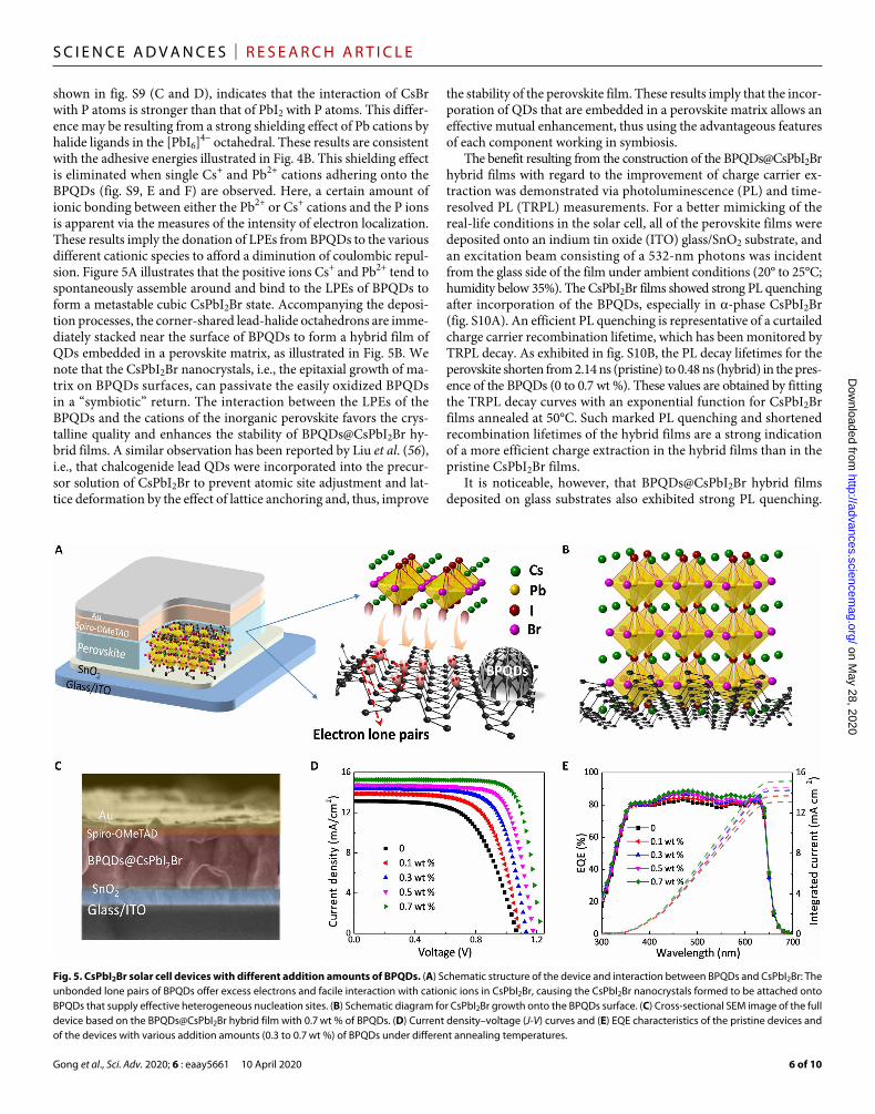
shown in fig. S9 (C and D), indicates that the interaction of CsBr with P atoms is stronger than that of PbI2 with P atoms. This differ-ence may be resulting from a strong shielding effect of Pb cations by halide ligands in the [PbI6]4− octahedral. These results are consistent with the adhesive energies illustrated in Fig. 4B. This shielding effect is eliminated when single Cs+ and Pb2+ cations adhering onto the BPQDs (fig. S9, E and F) are observed. Here, a certain amount of ionic bonding between either the Pb2+ or Cs+ cations and the P ions is apparent via the measures of the intensity of electron localization. These results imply the donation of LPEs from BPQDs to the various different cationic species to afford a diminution of coulombic repul-sion. Figure 5A illustrates that the positive ions Cs+ and Pb2+ tend to spontaneously assemble around and bind to the LPEs of BPQDs to form a metastable cubic CsPbI2Br state. Accompanying the deposi-tion processes, the corner-shared lead-halide octahedrons are imme-diately stacked near the surface of BPQDs to form a hybrid film of QDs embedded in a perovskite matrix, as illustrated in Fig. 5B. We note that the CsPbI2Br nanocrystals, i.e., the epitaxial growth of ma-trix on BPQDs surfaces, can passivate the easily oxidized BPQDs in a “symbiotic” return. The interaction between the LPEs of the BPQDs and the cations of the inorganic perovskite favors the crys-talline quality and enhances the stability of BPQDs@CsPbI2Br hy-brid films. A similar observation has been reported by Liu et al. (56), i.e., that chalcogenide lead QDs were incorporated into the precur-sor solution of CsPbI2Br to prevent atomic site adjustment and lat-tice deformation by the effect of lattice anchoring and, thus, improve
the stability of the perovskite film. These results imply that the incor-poration of QDs that are embedded in a perovskite matrix allows an effective mutual enhancement, thus using the advantageous features of each component working in symbiosis.
The benefit resulting from the construction of the BPQDs@CsPbI2Br hybrid films with regard to the improvement of charge carrier ex-traction was demonstrated via photoluminescence (PL) and time- resolved PL (TRPL) measurements. For a better mimicking of the real-life conditions in the solar cell, all of the perovskite films were deposited onto an indium tin oxide (ITO) glass/SnO2 substrate, and an excitation beam consisting of a 532-nm photons was incident from the glass side of the film under ambient conditions (20° to 25°C; humidity below 35%). The CsPbI2Br films showed strong PL quenching after incorporation of the BPQDs, especially in -phase CsPbI2Br (fig. S10A). An efficient PL quenching is representative of a curtailed charge carrier recombination lifetime, which has been monitored by TRPL decay. As exhibited in fig. S10B, the PL decay lifetimes for the perovskite shorten from 2.14 ns (pristine) to 0.48 ns (hybrid) in the pres-ence of the BPQDs (0 to 0.7 wt %). These values are obtained by fitting the TRPL decay curves with an exponential function for CsPbI2Br films annealed at 50°C. Such marked PL quenching and shortened recombination lifetimes of the hybrid films are a strong indication of a more efficient charge extraction in the hybrid films than in the pristine CsPbI2Br films.
It is noticeable, however, that BPQDs@CsPbI2Br hybrid films deposited on glass substrates also exhibited strong PL quenching.
Fig. 5. CsPbI2Br solar cell devices with different addition amounts of BPQDs. (A) Schematic structure of the device and interaction between BPQDs and CsPbI2Br: The unbonded lone pairs of BPQDs offer excess electrons and facile interaction with cationic ions in CsPbI2Br, causing the CsPbI2Br nanocrystals formed to be attached onto BPQDs that supply effective heterogeneous nucleation sites. (B) Schematic diagram for CsPbI2Br growth onto the BPQDs surface. (C) Cross-sectional SEM image of the full device based on the BPQDs@CsPbI2Br hybrid film with 0.7 wt % of BPQDs. (D) Current density–voltage (J-V) curves and (E) EQE characteristics of the pristine devices and of the devices with various addition amounts (0.3 to 0.7 wt %) of BPQDs under different annealing temperatures.
on May 28, 2020
http://advances.sciencemag.org/
Dow
nloaded from

Gong et al., Sci. Adv. 2020; 6 : eaay5661 10 April 2020
S C I E N C E A D V A N C E S | R E S E A R C H A R T I C L E
7 of 10
The corresponding PL lifetimes are obviously shorter than that of the pristine perovskite film (fig. S10C). Compared to the pristine CsPbI2Br film, the intensity of PL quenching of hybrid films depos-ited on electron transfer layer (declining to one-eighth of the pristine film) is far greater than that deposited on glass substrates (declining to two-thirds of the pristine film), further confirming the superior charge extraction performance of BPQDs@CsPbI2Br hybrid films in the unique heterojunction structure. This suggests that BPQDs embedded in the perovskite matrix film not only function as seeds assisting the formation of BPQDS/CsPbI2Br core-shell but also accel-erate charge transfer (39). The rapid charge transport could be attributed to the heterojunction hybrid interface formed with CsPbI2Br during the modulation of the nucleation and growth of perovskite by BPQDS. As illustrated in the band alignment (fig. S10D), BP QDs and CsPbI2Br pe-rovskite constitute a typical type II heterojunction (42, 57). To quantita-tively compare the trap states in CsPbI2Br and hybrid films, hole-only and electron-only devices were fabricated and characterized using the evolved space charge–limited current method (fig. S11). As shown in table S3, the trap density of BPQDs@CsPbI2Br hybrid films (Ne = 1.86 × 10⁻¹⁶ cm−3, Nh = 5.18 × 10⁻¹⁶ cm−3) are significantly reduced compared with that in the pristine CsPbI2Br film (Ne = 3.42 × 10⁻¹⁶ cm−3, Nh = 7.29 × 10⁻¹⁶ cm−3). Furthermore, the hole and electron mobility of hybrid films is higher than that of the pristine film based on Mott- Gurney’s equation (see table S3). These results further confirm the better charge transport characteristics of type II system and the for-mation of highly crystalline perovskite film after BPQD incorporation, which assists in improving the performance of hybrid film–based PSCs (39, 57).
Photovoltaic experiments were conducted to evaluate the per-formance of BPQDs@CsPbI2Br hybrid film–based devices using planar heterojunction architecture under different annealing tem-peratures. Figure 5C shows a precise cross-sectional SEM image of BPQDs@CsPbI2Br hybrid film–based device. PSCs, based on the black tetragonal -phase BPQDs@CsPbI2Br hybrid films annealed at 50°C, demonstrated a superior performance (Fig. 5D and Table 1) to the pristine devices, which exhibited a PCE of 9.26%, an open cir-cuit voltage (VOC) of 1.07 V, a short circuit current density (JSC) of 13.23 mA cm−2, and a fill factor (FF) of 0.65. The PCE increased as the amount of BPQDs increased. This observation could be attributed to the improved crystallinity of the active films. The PCE reached a maximum of 13.26% with 1.17 V, 14.95 mA cm−2, and 0.75 for the VOC, JSC, and FF parameters, respectively, when using 0.7 wt % of BPQDs contained in the -phase hybrid film (device B). Obviously, the improvement in the PCE mainly resulted from an increased FF
along with a slightly enhanced VOC and JSC, once again contributing to enhanced carrier extraction and transport efficiency of the hy-brid devices. PSCs were likewise fabricated to make more in-depth investigations on the cell performance when using the black cubic -phase BPQDs@CsPbI2Br hybrid film containing 0.7 wt % BPQDs.
The -phase BPQDs@CsPbI2Br hybrid-based film, device C, demonstrated the highest PCE of 15.47% due to augmentations in JSC (15.86 mA cm−2), VOC (1.25 V), and FF (0.78). For the control devices’ performance obtained under the same annealing parame-ters, see table S4. The corresponding external quantum efficiency (EQE) from 300 to 700 nm was measured and is shown in Fig. 5E. Device C exhibited high EQE values of more than 80% between 350 and 550 nm. The JSC calculated from the full EQE spectrum is in good agreement with the J-V measurements. The enhancement of EQE is consistent with the slightly enhanced light absorption in the wave-length region from 400 to 600 nm that was attributed to the compact and large grains of the BPQDs@CsPbI2Br hybrid film (fig. S12). The long-term moisture stability of the simple encapsulated CsPbI2Br de-vices was likewise examined after having been kept in a container under ambient conditions for 500 hours (temperature ≈ 28°C and humidity ≈ 35 to 45 RH%) in the dark. Both devices A and B degraded markedly during the 500-hour storage time to 50% of the initial effi-ciency of the fresh devices, whereas the cubic BPQDs@CsPbI2Br hy-brid film–based device C maintained 80% of its initial value (fig. S13). Comparatively, device B exhibited a more stable PCE performance than that of the pristine device A. The results demonstrate that the BPQDs@CsPbI2Br hybrid film–based PSCs have high stability and efficiency, especially the high-symmetry cubic hybrid film device.
Transient photocurrent/photovoltage decay measurements (TPC/TPV) were performed to complete the examination of the processes of carrier transportation and recombination in full devices under am-bient conditions (20° to 25°C; humidity below 25%) under illumina-tion with various intensities (fig. S14). Figure S15 shows the carrier transport lifetimes (tr) and recombination lifetimes (re) for devices A and C by fitting the TPC/TPV curves with an exponential function under varying light intensity. Device C exhibited a shorter carrier transport lifetime and an extra-long recombination lifetime compared to device A, implying faster charge diffusion and a low-charge recom-bination probability (58). As mentioned previously, these results cor-roborate the combined effects of strong binding among the perovskite precursor molecules, the BPQDs, and the SnO2 substrate, as well as the improved crystallinity of the CsPbI2Br perovskite film with an incorporation of 0.7 wt % BPQDs. According to D = d2/(c ∙ tr)D = d2/(c ∙ tr) (d is the absorber thickness, c is a constant of 2.37 being
Table 1. Device performance of perovskite solar cells. Pristine and differing weight volumes, x, of BPQDs.
CsPbI2Br + xBPQDs*(black films)
Jsc(mA/cm2)
Jsc-AVE(mA/cm2)
Voc(V)
FF(%)
PCE(%)
PCEAVE(%)
50°C/10 min x = 0 13.23 11.52 ± 0.20 1.07 64 9.26 8.97 ± 0.96
x = 0.3 wt % 13.92 12.13 ± 0.11 1.09 67 10.22 9.72 ± 0.74
x = 0.5 wt % 14.38 13.47 ± 0.23 1.13 72 11.78 10.25 ± 0.94
x = 0.7 wt % 14.95 13.61 ± 0.15 1.17 75 13.23 12.38 ± 0.84
50–200°C† x = 0.7 wt % 15.86 14.85 ± 0.34 1.25 78 15.47 14.80 ± 0.76*All of the deposited perovskite films rested for 30 min before annealing in glove box. †BPQDs@CsPbI2Br hybrid film with 0.7 wt % BPQDs was gradually annealed from 50° to 200°C at a ramp rate of 50°C (10 min)−1.
on May 28, 2020
http://advances.sciencemag.org/
Dow
nloaded from

Gong et al., Sci. Adv. 2020; 6 : eaay5661 10 April 2020
S C I E N C E A D V A N C E S | R E S E A R C H A R T I C L E
8 of 10
correlated to the charge conduction that can happen more from a hopping mechanism than from a band conduction mechanism in most of the semiconducting nanocrystal materials, and D is the carrier diffusion coefficient), the electron and hole diffusion coefficients in device C were estimated to be 2.42 × 10⁻³ cm2 s−1 and 2.31 × 10⁻³ cm2 s−1. These obtained values are slightly higher than those of device A (see table S5) but significantly lower than those obtained for pure perovskite thin layers with ultrafast spectroscopy characteriza-tion. These numbers could reflect the slowest electron and/or hole transfer process in the PSC devices under illumination, presumably through the perovskite/charge transport layer interfaces. The carrier diffusion lengths ( L = √
_ D ∙ re ) were evaluated for both devices. De-
vice C shows longer diffusion lengths equal to 604 nm for electrons and 489 nm for holes, compared with the values of 463 nm for elec-trons and 202 nm for holes in device A. The carrier transport dynam-ics in perovskite materials are sensitive to defect states and charge trapping. An enhanced carrier diffusion length indicates excellent car-rier transport capacity of the mixed cation perovskite film with incor-poration of 0.7 wt % of BPQDs.
DISCUSSIONWe demonstrated a simple solution-based method to synthesize high- quality and stable cubic phase CsPbI2Br films through the incorpora-tion of BPQDs, and a particular weight percentage of these QDs added to the pristine film provides effective heterogeneous nucleation sites, thus facilitating the CsPbI2Br nucleation and crystalline growth. This “BPQD-seeded” growth technique substantially improves the film morphology and shortens the phase transition period to obtain a pure -phase CsPbI2Br. An electronic donor-acceptor–like bonding could form between the BPQDs and CsPbI2Br using the chemical driving force derived from the diminution of coulombic repulsion, with LPEs of BPQDs exhibiting large coulombic repulsion acting as an electron donor. The strong interaction of intermolecular combina-tion provides an effective mutual enhancement, leading to superior electron-extracting efficiency as well as to stabilization of the inorganic perovskite CsPbI2Br framework. An impressive PCE of 15.47%, in addition to excellent moisture stability properties, could be achieved for the hybrid film device, BPQD@CsPbI2Br (0.7 wt %). Through implementation of sophisticated physical technique studies, we dis-close the contributions of BPQDs in CsPbI2Br for crystallization enhancement and carrier transport in the perovskite films. This ap-proach provides a facile method toward developing stable and effi-cient inorganic PSCs.
MATERIALS AND METHODSSynthesis of BPQDsThe BPQDs were prepared by using a facile liquid exfoliation method involving probe sonication followed by bath sonication of ground powders of bulk BP (43, 44). In brief, 100-mg BP crystals were grinded into BP powders and then added into a 100-ml sealed conical tube with 50-ml N-methyl pyrrolidone (NMP) and sonicated with a sonic tip for 6 hours at a power of 1200 W in an ice bath. The ultrasonic fre-quency was taken from 19 to 25 kHz and the duty cycle (4 s on and 4 s off). The dispersion was sonicated in an ice bath for 3 hours at a pow-er of 200 W. The resultant dispersion was centrifuged for 20 min at 7000 rpm. The supernatant containing BPQDs was decanted gently. Then, the BPQD suspension in NMP was centrifuged at 12,000 rpm
for 20 min, and the precipitate was repeated mixed solvent of DMF and DMSO (volume ratio of 9:1) rinsing and resuspended in the mixed solution. Last, the BPQD solutions with different concentra-tions were obtained by diluting with DMF and DMSO (volume ratio of 9:1) mixture solvent.
The CsPbI2Br-BPQD hybrid precursor solutionThe pure CsPbI2Br precursor solution was prepared by dissolving CsBr:PbI2 (1:1) in a mixed solvent of DMF and DMSO (volume ratio of 9:1) at 0.85 M in a N2 glove box while stirring for 1 hour at room temperature. The BPQDs@CsPbI2Br hybrid precursor solution was prepared by dissolving 0.85 M CsBr:PbI2 (1:1) in the preformed BPQD dispersion solution, with corresponding mass fractions of BPQDs in the hybrid precursor solution, with respect to the total solute weight of the perovskite precursor and BPQDs, from 0.1 to 3 wt %.
Device fabricationAn SnO2 electron transport layer (ETL) with 50 nm thickness was prepared by spin-coating of a SnCl2.2H2O (Alfa, anhydrous 99.9985%) solution. SnCl2.2H2O (0.05 M) in ethanol solution was spin-coated twice onto the precleaned ITO/glass substrate (O2 plasma treatment) at 4000 rpm for 30 s under the annealing conditions of 180°C for 1 hour in an ambient atmospheric environment. After cooling to room temperature, the samples were treated again with UV-O3 for 30 min and transferred to a glove box for perovskite deposition. The CsPbI2Br and/or CsPbI2Br-BPQD hybrid films were coated on the ETL by spin-coating the precursor solution at 600 rpm for 4 s, fol-lowed by 2000 rpm for 26 s. All of the deposited perovskite films rested for 30 min before annealing. The CsPbI2Br consisting of 0 to 0.7 wt % of BPQDs was annealed at 50°C for 10 min to achieve black tetragonal -phase CsPbI2Br films and an -phase CsPbI2Br film with 0.7 wt % BPQD through gradual annealing from 50° to 200°C at a ramp rate of 25°C min−1 in a N2-filled glove box. Spiro-OMeTAD (72.3 mg ml−1; Lumtec) solution in chlorobenzene with 28.8 l of 4-tert-Butylpyridine (tBP) and 17.5 l of bistrifluoromethanesulfonimide lithium salt/acetonitrile (520 mg ml−1) was used as the hole transport layer (HTL) solution, which was spin-coated onto the perovskite films at 5000 rpm for 40 s. Last, an 80-nm gold counter electrode (mask area of 0.108 cm2) was thermally deposited onto the HTL layer under vacuum at 2 × 10⁻⁵ torr.
CharacterizationTEM and HRTEM analyses were carried out using an FEI SIRIS microscope. XPS was used to study the elemental composition of the pure and BPQD-doped CsPbI2Br by a Kratos AXIS Ultra-DLD ultrahigh-vacuum photoemission spectroscopy system with an Al K radiation source. The surface morphology of perovskite films was characterized by field-emission SEM. The in situ variable- temperature XRD intensities of the perovskite films were measured by XRD (Shimadzu XRD-6100 diffractometer with Cu K -radiation). The fluorescence images of perovskite films were captured on an Olympus FV1000 inverted fluorescence microscope. Steady-state PL and TRPL decay of the pure and BPQD-doped CsPbI2Br were con-ducted using time-resolved luminescence decay with a time-correlated single-photo counting system (PicoHarp 300, PicoQuant GmbH). A laser beam with an excitation wavelength of 532 nm was used to excite the samples from the perovskite layer side. The excitation light source was a Ti:sapphire laser (Mira 900, Coherent; 76 MHz, 130 fs). The pho-tocurrent density-voltage (J-V) characteristics of PSCs were measured
on May 28, 2020
http://advances.sciencemag.org/
Dow
nloaded from

Gong et al., Sci. Adv. 2020; 6 : eaay5661 10 April 2020
S C I E N C E A D V A N C E S | R E S E A R C H A R T I C L E
9 of 10
under 1 sun illumination using a programmable Keithley 2400 digital source meter under AM1.5 G simulated sunlight at 100 mW cm−2 (Oriel, model 91192). The intensity of simulated light was precisely calibrated with a NREL-certified KG5-filtered Si photodiode detec-tor. The active area of solar cell was determined to be 0.108 cm2 by a black metal mask. The incident photon conversion efficiency (IPCE) was measured on a Newport IPCE system (Newport, USA). A white-light bias (10% sun light intensity) was applied onto the sample during the IPCE measurements with the alternating current model (130 Hz). Photovoltage/photocurrent transient decay measurements were carried out to obtain the electron diffusion lengths (Hua Ming, model III). A white-light bias on the device sample was generated from an array of diodes. The triggering of the array of red laser pulses was controlled by a fast solid-state switch. Transient decays were mea-sured at different white-light intensities by tuning the voltage applied to the diodes. The voltage output was recorded on an oscilloscope directly connected to the cells. The space-charge-limited current (SCLC) measurement was performed using Keithley 2400 digital source in the dark, under ambient conditions (20° to 25°C; humidity below 25%).
SUPPLEMENTARY MATERIALSSupplementary material for this article is available at http://advances.sciencemag.org/cgi/content/full/6/15/eaay5661/DC1
REFERENCES AND NOTES 1. NREL, Best Research-Cell Efficiencies (2019); https://www.nrel.gov/pv/cell-efficiency.html. 2. X. Gong, M. Li, X.-B. Shi, H. Ma, Z.-K. Wang, L.-S. Liao, Controllable perovskite
crystallization by water additive for high-performance solar cells. Adv. Funct. Mater. 25, 6671–6678 (2015).
3. X. Gong, L. Guan, H. Pan, Q. Sun, X. Zhao, H. Li, H. Pan, Y. Shen, Y. Shao, L. Sun, Z. Cui, L. Ding, M. Wang, Highly efficient perovskite solar cells via nickel passivation. Adv. Funct. Mater. 28, 1804286 (2018).
4. N. H. Nickel, F. Lang, V. V. Brus, O. Shargaieva, J. Rappich, Unraveling the light-induced degradation mechanisms of CH3NH3PbI3 perovskite films. Adv. Electron. Mater. 3, 1700158 (2017).
5. A. F. Akbulatov, S. Y. Luchkin, L. A. Frolova, N. N. Dremova, K. L. Gerasimov, I. S. Zhidkov, D. V. Anokhin, E. Z. Kurmaev, K. J. Stevenson, P. A. Troshin, Probing the intrinsic thermal and photochemical stability of hybrid and inorganic lead halide perovskites. J. Phys. Chem. Lett. 8, 1211–1218 (2017).
6. W. Zhou, Y. Zhao, X. Zhou, R. Fu, Q. Li, Y. Zhao, K. Liu, D. Yu, Q. Zhao, Light-independent ionic transport in inorganic perovskite and ultrastable Cs-based perovskite solar cells. J. Phys. Chem. Lett. 8, 4122–4128 (2017).
7. R. F. Service, Cesium fortifies next-generation solar cells. Science 351, 113–114 (2016). 8. A. Swarnkar, A. R. Marshall, E. M. Sanehira, B. D. Chernomordik, D. T. Moore,
J. A. Christians, T. Chakrabarti, J. M. Luther, Quantum dot-induced phase stabilization of -CsPbI3 Perovskite for high-efficiency photovoltaics. Science 354, 92–95 (2016).
9. T. Zhang, M. I. Dar, G. Li, F. Xu, N. Guo, M. Grätzel, Y. Zhao, Bication lead iodide 2D perovskite component to stabilize inorganic -CsPbI3 perovskite phase for high-efficiency solar cells. Sci. Adv. 3, e1700841 (2017).
10. G. E. Eperon, G. M. Paternò, R. J. Sutton, A. Zampetti, A. A. Haghighirad, F. Cacialli, H. J. Snaith, Inorganic caesium lead iodide perovskite solar cells. J. Mater. Chem. A 3, 19688–19695 (2015).
11. W. Ahmad, J. Khan, G. Niu, J. Tang, Inorganic CsPbI3 perovskite-based solar cells: A choice for a tandem device. Sol. RRL 1, 1700048 (2017).
12. Z. Zeng, J. Zhang, X. Gan, H. Sun, M. Shang, D. Hou, C. Lu, R. Chen, Y. Zhu, L. Han, In situ grain boundary functionalization for stable and efficient inorganic CsPbI2Br perovskite solar cells. Adv. Energy Mater. 8, 1801050 (2018).
13. R. J. Sutton, G. E. Eperon, L. Miranda, E. S. Parrott, B. A. Kamino, J. B. Patel, M. T. Hörantner, M. B. Johnston, A. A. Haghighirad, D. T. Moore, H. J. Snaith, Bandgap-tunable cesium lead halide perovskites with high thermal stability for efficient solar cells. Adv. Energy Mater. 6, 1502458 (2016).
14. M. Wang, W.-L. Yim, P. Liao, Y. Shen, Temperature dependent characteristics of perovskite solar cells. ChemistrySelect 2, 4469–4477 (2017).
15. R. E. Beal, D. J. Slotcavage, T. Leijtens, A. R. Bowring, R. A. Belisle, W. H. Nguyen, G. F. Burkhard, E. T. Hoke, M. D. McGehee, Cesium lead halide perovskites with improved stability for tandem solar cells. J. Phys. Chem. Lett. 7, 746–751 (2016).
16. X. Xu, M. Wang, Photocurrent hysteresis related to ion motion in metal-organic perovskites. Sci. China Chem. 60, 396–404 (2017).
17. J. K. Nam, D. H. Chun, R. J. K. Rhee, J. H. Lee, J. H. Park, Methodologies toward efficient and stable cesium lead halide perovskite-based solar cells. Adv. Sci. 5, 1800509 (2018).
18. G. E. Eperon, E. Jedlicka, D. S. Ginger, Biexciton auger recombination differs in hybrid and inorganic halide perovskite quantum dots. J. Phys. Chem. Lett. 9, 104–109 (2018).
19. A. H. Hill, K. E. Smyser, C. L. Kennedy, E. S. Massaro, E. M. Grumstrup, Screened charge carrier transport in methylammonium lead iodide perovskite thin films. J. Phys. Chem. Lett. 8, 948–953 (2017).
20. H. Zhu, K. Miyata, Y. Fu, J. Wang, P. P. Joshi, D. Niesner, K. W. Williams, S. Jin, X. Y. Zhu, Screening in crystalline liquids protects energetic carriers in hybrid perovskites. Science 353, 1409–1413 (2016).
21. C. L. Kennedy, A. H. Hill, E. S. Massaro, E. M. Grumstrup, Ultrafast excited-state transport and decay dynamics in cesium lead mixed halide perovskites. ACS Energy Lett. 2, 1501–1506 (2017).
22. J. K. Nam, S. U. Chai, W. Cha, Y. J. Choi, W. Kim, M. S. Jung, J. Kwon, D. Kim, J. H. Park, Potassium incorporation for enhanced performance and stability of fully inorganic cesium lead halide perovskite solar cells. Nano Lett. 17, 2028–2033 (2017).
23. C. F. J. Lau, M. Zhang, X. Deng, J. Zheng, J. Bing, Q. Ma, J. Kim, L. Hu, M. A. Green, S. Huang, A. Ho-Baillie, Strontium-doped low-temperature-processed CsPbI2Br perovskite solar cells. ACS Energy Lett. 2, 2319–2325 (2017).
24. D. Bai, J. Zhang, Z. Jin, H. Bian, K. Wang, H. Wang, L. Liang, Q. Wang, S. F. Liu, Interstitial Mn2+-driven high-aspect-ratio grain growth for low-trap-density microcrystalline films for record efficiency CsPbI2Br solar cells. ACS Energy Lett. 3, 970–978 (2018).
25. C.-Y. Chen, H.-Y. Lin, K.-M. Chiang, W.-L. Tsai, Y.-C. Huang, C.-S. Tsao, H.-W. Lin, All-vacuum-deposited stoichiometrically balanced inorganic cesium lead halide perovskite solar cells with stabilized efficiency exceeding 11%. Adv. Mater. 29, 1605290 (2017).
26. J. K. Nam, M. S. Jung, S. U. Chai, Y. J. Choi, D. Kim, J. H. Park, Unveiling the crystal formation of cesium lead mixed-halide perovskites for efficient and stable solar cells. J. Phys. Chem. Lett. 8, 2936–2940 (2017).
27. W. Chen, H. Chen, G. Xu, R. Xue, S. Wang, Y. Li, Y. Li, Precise control of crystal growth for highly efficient CsPbI2Br perovskite solar cells. Joule 3, 191–204 (2018).
28. S.-S. Li, C.-H. Chang, Y.-C. Wang, C.-W. Lin, D.-Y. Wang, J.-C. Lin, C.-C. Chen, H.-S. Sheu, H.-C. Chia, W.-R. Wu, U.-S. Jeng, C.-T. Liang, R. Sankar, F.-C. Chou, C.-W. Chen, Intermixing-seeded growth for high-performance planar heterojunction perovskite solar cells assisted by precursor-capped nanoparticles. Energ. Environ. Sci. 9, 1282–1289 (2016).
29. J. Han, S. Luo, X. Yin, Y. Zhou, H. Nan, J. Li, X. Li, D. Oron, H. Shen, H. Lin, Hybrid PbS quantum-dot-in-perovskite for high-efficiency perovskite solar cell. Small 14, 1801016 (2018).
30. J. Han, X. Yin, H. Nan, Y. Zhou, Z. Yao, J. Li, D. Oron, H. Lin, Enhancing the performance of perovskite solar cells by hybridizing SnS quantum dots with CH3NH3PbI3. Small 13, 1700953 (2017).
31. Y. W. Wang, S. Liu, B. W. Zeng, H. Huang, J. Xiao, J. B. Li, M. Q. Long, S. Xiao, X. F. Yu, Y. L. Gao, J. He, Ultraviolet saturable absorption and ultrafast carrier dynamics in ultrasmall black phosphorus quantum dots. Nanoscale 9, 4683–4690 (2017).
32. Y. Xu, Z. Wang, Z. Guo, H. Huang, Q. Xiao, H. Zhang, X.-F. Yu, Solvothermal synthesis and ultrafast photonics of black phosphorus quantum dots. Adv. Opt. Mater. 4, 1223–1229 (2016).
33. Y. Wei, R. Long, Grain boundaries are benign and suppress nonradiative electron-hole recombination in monolayer black phosphorus: A time-domain Ab initio study. J. Phys. Chem. Lett. 9, 3856–3862 (2018).
34. R. Long, W. Fang, A. V. Akimov, Nonradiative electron–Hole recombination rate is greatly reduced by defects in monolayer black phosphorus: Ab initio time domain study. J. Phys. Chem. Lett. 7, 653–659 (2016).
35. S. Liu, S. Lin, P. You, C. Surya, S. P. Lau, F. Yan, Black phosphorus quantum dots used for boosting light harvesting in organic photovoltaics. Angew. Chem. Int. Ed. Engl. 56, 13717–13721 (2017).
36. W. Chen, K. Li, Y. Wang, X. Feng, Z. Liao, Q. Su, X. Lin, Z. He, Black phosphorus quantum dots for hole extraction of typical planar hybrid perovskite solar cells. J. Phys. Chem. Lett. 8, 591–598 (2017).
37. N. Fu, C. Huang, P. Lin, M. Zhu, T. Li, M. Ye, S. Lin, G. Zhang, J. Du, C. Liu, B. Xu, D. Wang, S. Ke, Black phosphorus quantum dots as dual-functional electron-selective materials for efficient plastic perovskite solar cells. J. Mater. Chem. A 6, 8886–8894 (2018).
38. W. Yang, J. Chen, X. Lian, J. Li, F. Yao, G. Wu, W. Qiu, C. Jin, P. Heremans, H. Chen, Black phosphorus quantum dots induced high-quality perovskite film for efficient and thermally stable planar perovskite solar cells. Sol. RRL 3, 1900132 (2019).
39. Y. Wang, H. Zhang, T. Zhang, W. Shi, M. Kan, J. Chen, Y. Zhao, Photostability of MAPbI3 perovskite solar cells by incorporating black phosphorus. Sol. RRL 3, 1900197 (2019).
40. H. Huang, J. Li, Y. Yi, J. Wang, Y. Kang, P. K. Chu, H. C. Ong, X. F. Yu, In situ growth of all-inorganic perovskite nanocrystals on black phosphorus nanosheets. Chem. Commun. 54, 2365–2368 (2018).
on May 28, 2020
http://advances.sciencemag.org/
Dow
nloaded from

Gong et al., Sci. Adv. 2020; 6 : eaay5661 10 April 2020
S C I E N C E A D V A N C E S | R E S E A R C H A R T I C L E
10 of 10
41. J. Dai, X. C. Zeng, Bilayer phosphorene: Effect of stacking order on bandgap and its potential applications in thin-film solar cells. J. Phys. Chem. Lett. 5, 1289–1293 (2014).
42. B. Liu, M. Long, M.-Q. Cai, J. Yang, Interface engineering of CsPbI3-black phosphorus van der Waals heterostructure. Appl. Phys. Lett. 112, 043901 (2018).
43. S. Zhengbo, X. Hanhan, T. Siying, Y. Xue-Feng, G. Zhinan, S. Jundong, Z. Han, H. Hao, W. Huaiyu, P. K. Chu, Ultrasmall black phosphorus quantum dots: Synthesis and use as photothermal agents. Angew. Chem. Int. Ed. 54, 11526–11530 (2015).
44. P. Yasaei, B. Kumar, T. Foroozan, C. Wang, M. Asadi, D. Tuschel, J. E. Indacochea, R. F. Klie, A. Salehi-Khojin, High-quality black phosphorus atomic layers by liquid-phase exfoliation. Adv. Mater. 27, 1887–1892 (2015).
45. Y. Fu, M. T. Rea, J. Chen, D. J. Morrow, M. P. Hautzinger, Y. Zhao, D. Pan, L. H. Manger, J. C. Wright, R. H. Goldsmith, S. Jin, Selective stabilization and photophysical properties of metastable perovskite polymorphs of CsPbI3 in thin films. Chem. Mater. 29, 8385–8394 (2017).
46. C. Liu, W. Li, J. Chen, J. Fan, Y. Mai, R. E. I. Schropp, Ultra-thin MoOx as cathode buffer layer for the improvement of all-inorganic CsPbIBr2 perovskite solar cells. Nano Energy 41, 75–83 (2017).
47. N. J. Jeon, J. H. Noh, Y. C. Kim, W. S. Yang, S. Ryu, S. I. Seok, Solvent engineering for high-performance inorganic-organic hybrid perovskite solar cells. Nat. Mater. 13, 897–903 (2014).
48. C. C. Stoumpos, M. G. Kanatzidis, The renaissance of halide perovskites and their evolution as emerging semiconductors. Acc. Chem. Res. 48, 2791–2802 (2015).
49. Z. Dang, J. Shamsi, F. Palazon, M. Imran, Q. A. Akkerman, S. Park, G. Bertoni, M. Prato, R. Brescia, L. Manna, In situ transmission electron microscopy study of electron beam-induced transformations in colloidal cesium lead halide perovskite nanocrystals. ACS Nano 11, 2124–2132 (2017).
50. Y. Zhao, H. Wang, H. Huang, Q. Xiao, Y. Xu, Z. Guo, H. Xie, J. Shao, Z. Sun, W. Han, X. F. Yu, P. Li, P. K. Chu, Surface coordination of black phosphorus for robust air and water stability. Angew. Chem. Int. Ed. Engl. 55, 5003–5007 (2016).
51. C. Liu, W. Li, H. Li, H. Wang, C. Zhang, Y. Yang, X. Gao, Q. Xue, H.-L. Yip, J. Fan, R. E. I. Schropp, Y. Mai, Structurally reconstructed CsPbI2Br perovskite for highly stable and square-centimeter all-inorganic perovskite solar cells. Adv. Energy Mater. 9, 1803572 (2019).
52. X. P. Kong, X. Shen, J. Jang, X. Gao, Electron pair repulsion responsible for the peculiar edge effects and surface chemistry of black phosphorus. J. Phys. Chem. Lett. 9, 947–953 (2018).
53. V. V. Kulish, O. I. Malyi, C. Persson, P. Wu, Adsorption of metal adatoms on single-layer phosphorene. Phys. Chem. Chem. Phys. 17, 992–1000 (2014).
54. T. Hu, J. Hong, First-principles study of metal adatom adsorption on black phosphorene. J. Phys. Chem. C 119, 8199–8207 (2015).
55. G. M. Hettiarachchi, G. M. Pierzynski, M. D. Ransom, In situ stabilization of soil lead using phosphorus. J. Environ. Qual. 30, 1214–1221 (2001).
56. M. Liu, Y. Chen, C.-S. Tan, R. Quintero-Bermudez, A. H. Proppe, R. Munir, H. Tan, O. Voznyy, B. Scheffel, G. Walters, A. P. T. Kam, B. Sun, M.-J. Choi, S. Hoogland, A. Amassian, S. O. Kelley, F. P. García de Arquer, E. H. Sargent, Lattice anchoring stabilizes solution-processed semiconductors. Nature 570, 96–101 (2019).
57. Y. Zhao, T. L. Chen, L. Xiao, M. A. Kolaczkowski, L. Zhang, L. M. Klivansky, V. Altoe, B. Tian, J. Guo, X. Peng, Y. Tian, Y. Liu, Facile integration of low-cost black phosphorus in solution-processed organic solar cells with improved fill factor and device efficiency. Nano Energy 53, 345–353 (2018).
58. S. Liu, W. Huang, P. Liao, N. Pootrakulchote, H. Li, J. Lu, J. Li, F. Huang, X. Shai, X. Zhao, Y. Shen, Y. B. Cheng, M. Wang, 17% Efficient printable mesoscopic PIN metal oxide framework perovskite solar cells using cesium-containing triple cation perovskite. J. Mater. Chem. A 5, 22952–22958 (2017).
59. A. Marronnier, G. Roma, S. Boyer-Richard, L. Pedesseau, J. M. Jancu, Y. Bonnassieux, C. Katan, C. C. Stoumpos, M. G. Kanatzidis, J. Even, Anharmonicity and disorder in the black phases of cesium lead iodide used for stable inorganic perovskite solar cells. ACS Nano 12, 3477–3486 (2018).
60. J. Shao, H. Xie, H. Huang, Z. Li, Z. Sun, Y. Xu, Q. Xiao, X.-F. Yu, Y. Zhao, H. Zhang, H. Wang, P. K. Chu, Biodegradable black phosphorus-based nanospheres for in vivo photothermal cancer therapy. Nat. Commun. 7, 12967 (2016).
Acknowledgments: We thank the Analytical and Testing Centre of Huazhong University of Science & Technology (HUST) for the measurements of the samples. M.G. has a part-time affiliation with Max Planck Institute for Solid State Research, Stuttgart, Germany and Nanyang Technological University, Singapore. S.M.Z. has a part-time affiliation with King Abdulaziz University, Jeddah, Saudi Arabia. Funding: This work was financially supported by the Natural Science Foundation of China (nos. 21673091, 21975088, and 51802069) and the NSFC Major International (Regional) Joint Research Project (nos. 51661135023 and 51961165106). M.G. and S.M.Z. thank the financial support from the GRAPHENE Flagship Core 2 project supported by the European Commission H2020 Programme under contract 785219. Author contributions: X.G. conceived the ideas, conducted the device fabrication, performed the data analysis, and prepared the manuscript. L.G. provided the DFT calculations. Q.L. synthesized BPQDs. Y.L. measured the fluorescence images. T.Z. and H.P. performed the Raman and TEM measurement. Q.S. and Y.S. helped with the device measurement and data analysis. C.G. and S.M.Z. revised the manuscript. M.G. and M.W. guided and supervised the whole study. Competing interests: The authors declare that they have no competing interests. Data and materials availability: All data needed to evaluate the conclusions in the paper are present in the paper and/or the Supplementary Materials. Additional data related to this paper may be requested from the authors.
Submitted 29 June 2019Accepted 17 January 2020Published 10 April 202010.1126/sciadv.aay5661
Citation: X. Gong, L. Guan, Q. Li, Y. Li, T. Zhang, H. Pan, Q. Sun, Y. Shen, C. Grätzel, S. M. Zakeeruddin, M. Grätzel, M. Wang, Black phosphorus quantum dots in inorganic perovskite thin films for efficient photovoltaic application. Sci. Adv. 6, eaay5661 (2020).
on May 28, 2020
http://advances.sciencemag.org/
Dow
nloaded from

applicationBlack phosphorus quantum dots in inorganic perovskite thin films for efficient photovoltaic
Michael Grätzel and Mingkui WangXiu Gong, Li Guan, Qingwei Li, Yan Li, Tao Zhang, Han Pan, Qiang Sun, Yan Shen, Carole Grätzel, Shaik M. Zakeeruddin,
DOI: 10.1126/sciadv.aay5661 (15), eaay5661.6Sci Adv
ARTICLE TOOLS http://advances.sciencemag.org/content/6/15/eaay5661
MATERIALSSUPPLEMENTARY http://advances.sciencemag.org/content/suppl/2020/04/06/6.15.eaay5661.DC1
REFERENCES
http://advances.sciencemag.org/content/6/15/eaay5661#BIBLThis article cites 59 articles, 4 of which you can access for free
PERMISSIONS http://www.sciencemag.org/help/reprints-and-permissions
Terms of ServiceUse of this article is subject to the
is a registered trademark of AAAS.Science AdvancesYork Avenue NW, Washington, DC 20005. The title (ISSN 2375-2548) is published by the American Association for the Advancement of Science, 1200 NewScience Advances
License 4.0 (CC BY-NC).Science. No claim to original U.S. Government Works. Distributed under a Creative Commons Attribution NonCommercial Copyright © 2020 The Authors, some rights reserved; exclusive licensee American Association for the Advancement of
on May 28, 2020
http://advances.sciencemag.org/
Dow
nloaded from