materials processing center/microphotonics centerweb.mit.edu/annualreports/pres05/08.21.pdf · ·...
TRANSCRIPT
8–240
Materials Processing Center/Microphotonics Center
This report discusses the FY2005 activities of the Materials Processing Center (MPC) and its major affiliate, the Microphotonics Center (MPhC). The Materials Processing Center is an interdisciplinary center within MIT’s School of Engineering. The director is Professor Lionel Kimerling (Department of Materials Science and Engineering), and the associate director is Dr. George Kenney. The MPC, founded in 1980 by Professor Merton Flemings, is now celebrating a quarter century of advancing materials research at MIT.
The MPC was established in response to a recognized national need to improve the knowledge base and streamline technology transfer in the field of materials science and engineering. Materials science traverses all the physical sciences. Materials processing, as the MPC defines it, covers a wide range of types of materials and crosses traditional departmental and school boundaries.
The mission of the MPC is to provide an environment where students and professionals from industry, government, and academia collaborate to identify and address pivotal multidisciplinary issues in materials processing and manufacturing in a way that unites the MIT materials community, creates new knowledge, produces knowledgeable people (graduates/employees), and promotes the exchange of knowledge in the service of our country and in the context of the global community.
The MPC is a “virtual center,” without facilities, laboratory space, or equipment as such; it acts by bringing people and resources together in “intellectual space” to examine problems and pursue opportunities from a science-to-systems perspective.
The Microphotonics Center is a center within the MPC that builds interdisciplinary teams focused on advancing basic science and emerging technology to enable the evolution of photonics from single discrete devices to strongly integrated microphotonic components and systems. The MPhC and MPC share an overlapping staff in a common headquarters space.
This is a significant anniversary year for MPC, marking twenty-five years of advancing materials research at MIT. The activities section of this report provides more detail about the ways in which this achievement will be celebrated over the course of the coming year.
Relationships
The MPC/MPhC builds relationships with faculty by familiarizing itself with their current research projects, future interests, and resource needs; by bringing industries’ materials and processing needs and interests to them; and by inviting them individually or in teams to collaborate with industry. MPC provides seed research program development funding to new faculty members and teams and assists with proposals, budgets, and the administration of research accounts.
During FY2005, there were more than 50 faculty and senior research staff members with active accounts in the MPC; some 70 were included in the MPC’s research digest,
Materials Processing Center/Microphotonics Center
8–241
Materials Research at MIT, produced in collaboration with the Center for Materials Science and Engineering (CMSE). The faculty who have had some affiliation with the MPC hail from nine departments in the Schools of Engineering, Science, and Humanities, Arts, and Social Sciences, as well as the Sloan School of Management.
The MPC provides industry with guided access to MIT’s materials research community via its Industry Collegium (MPC) and Industry Consortium (MPhC). The MPC Industry Collegium is made up of more than 25 domestic and international companies in a range of industries, from traditional structural materials to biomaterials. The MPhC Industry Consortium consisted in FY2005 of member companies from the materials-to-systems technology supply chain of the computing, data-communications, and telecommunications sectors; the consortium’s Communications Technology Roadmap Project involves personnel from more than 40 companies and universities. For member companies, both the collegium and the consortium help to enable the realization of groundbreaking MIT research into market-changing products. The MPC/MPhC strategy includes leveraging core federal research funding within the MIT materials community into expanded industrial-academic collaborations. In addition to its collegium and consortium, the MPC and MPhC also have two major research alliance partnerships, as well as traditional research programs with individual companies.
The MPC has an active Industrial Advisory Board, comprised of industry leaders from a spectrum of small to large companies.
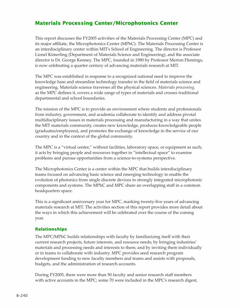
The MPC seeks to collaborate with other materials-related centers on campus, including CMSE, the Institute for Soldier Nanotechnology (ISN), the Research Laboratory for Electronics (RLE), Microsystems Technology Laboratory (MTL), and the Media Lab. Campus materials research volume across MPC, CMSE, ISN, and the Department of Materials Science and Engineering has steadily increased each year since 1999, reaching $37.3M for FY2004.
MPC and Materials Community Research Volume, FY1992–2004.
MIT Reports to the President 2004–2005
8–242
The MPC has also joined with CMSE to launch the Materials at MIT gateway initiative. Materials at MIT will be the internet gateway to the vibrant materials research community at MIT. The Materials at MIT website, now under development, will be the internet home for a repository of useful information related to materials research at MIT—and at the same time, the starting point from which a site visitor can reach any other point in the MIT materials research community. The site will feature:
• Detailed information about the full range of materials research projects under way at MIT
• News about the ho�est advances in materials science, engineering, and processing
• Pages about shared experimental facilities at MIT• Event listings for materials-related educational outreach activities• Links to the individual websites of every materials-related laboratory,
department, center, and professor on the MIT campus
The Materials at MIT initiative is being spearheaded by MPC and CMSE, but the participation of any and every materials-related organization on campus will be welcomed and encouraged.
Activities
Research Activities
MPC and MPhC total research volume was $9.4M in FY2005. Our three priority research areas are medical materials, photonics, and energy. During much of FY2005, the MPC continued to focus on the development of MPhC projects. The Microphotonics Center has several major research thrusts in addition to individual faculty members’ research: Within the Industry Consortium, there are the Communications Technology Roadmap Program and two consortium-funded seed research projects.
One particular focal area for the Microphotonics Center research is in new materials, structures, and architectures for planar lightwave circuits. The goal is fully integrated photonic functionality for these tiny, potentially low-cost units, thereby enabling their deployment both in metropolitan-area and fiber-to-the-X communications and in server and computing applications. Our areas of emphasis include dense wavelength-division multiplexing (a way of increasing signal capacity), optical signal conditioning, microwave signal processing, on-chip optical clock distribution, and I/O for microprocessors. Our research has set a number of world records for device performance and size.
Communications Technology Roadmap Program
The Microphotonics Center Industry Consortium (see below) began its key initiative, the Communications Technology Roadmap Project (h�p://mph-roadmap.mit.edu/), in the fall of 2000. This ongoing study has provided a 30-year view down the rapidly changing microphotonics technology highway with interviews of industry leaders at all levels of management within the materials-to-systems part of the technology supply chain and with consensus building on how technology and business issues will play
Materials Processing Center/Microphotonics Center
8–243
out. Consortium members can use the study findings in optical network architecture, component design and manufacturing, market analysis, technical supply chain analysis, and geographic analysis to focus their R&D and business strategies.
The photonics industry—whose contributions include the core technologies for fiber-optic communications systems—is on the cu�ing edge of technical innovation and application. Although historically, photonic components have been associated almost exclusively with the communications industry, they are now emerging in a variety of industries, including computation, information, lighting, displays, sensing and scanning, biometrics, manufacturing, and automotive. Today, the optical components industry stands at the threshold of a major expansion that will restructure its business processes and sustain its profitability for the next three decades.
Despite the fact that optical fiber has been used since the 1980s, current networks are still limited by the electrical interconnects at their termini. The opportunity to advance the speed of communications lies in replacing these slower components with photonic equivalents. As the end-to-end infrastructure becomes increasingly optical, network latency will decrease to the point that communications become perceptually instantaneous to users. The effect of such technology on transportation, commerce, education, entertainment, social interaction, and government will be dramatic. For instance, one only needs to look at the world 10 years ago to understand the social impact of the cell phone. The shi� to a real-time wideband network promises the same dramatic social effect.
More than 40 companies and universities have participated to date in MIT’s Communications Technology Roadmap (CTR) program, which has spent more than four years analyzing and charting a course for the future of photonics technology. Guided by industry-led Technology Working Groups (TWGs) with the support of MIT
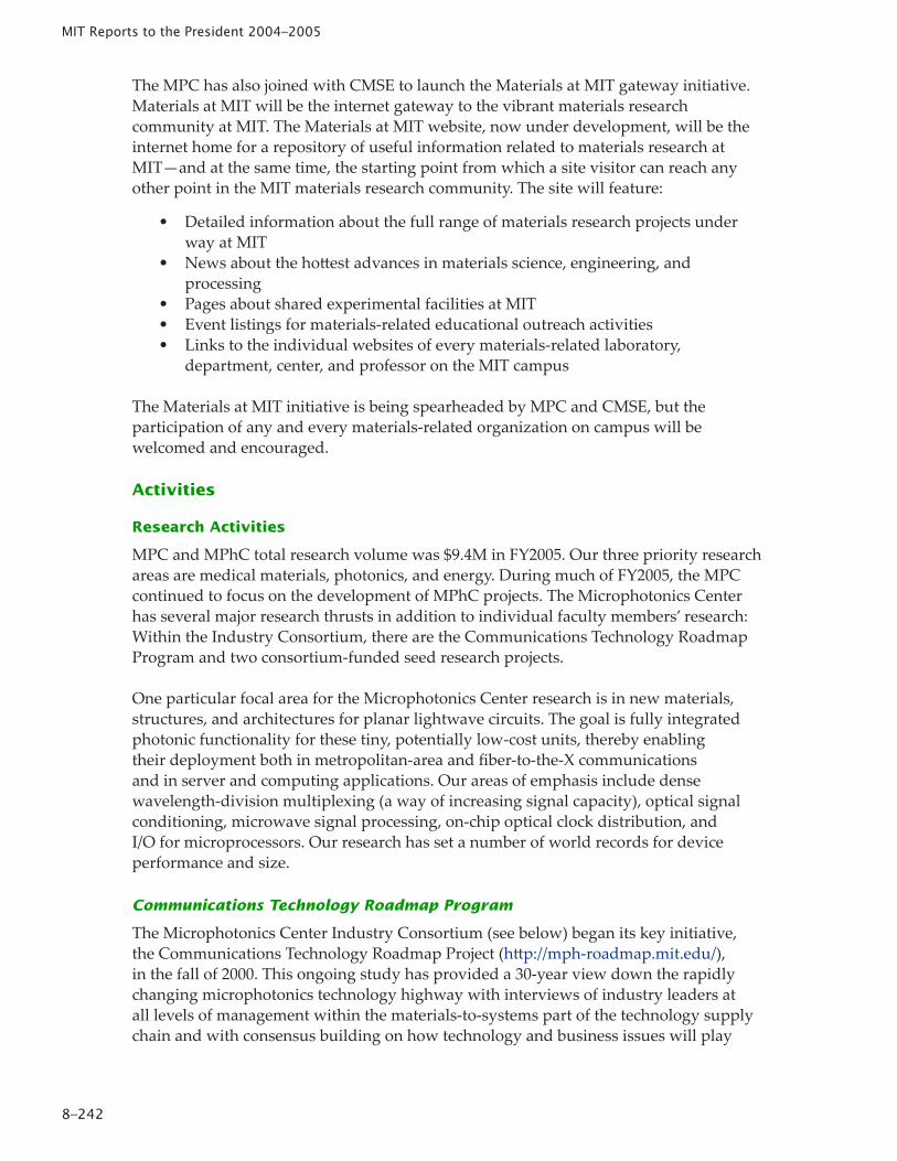
Across a range of communications technologies, 10 Mb/s × km has been the cross-over point to optical technology.
MIT Reports to the President 2004–2005
8–244
faculty and student analyses, the CTR program analyzes the current state of the photonic components industry, the role of emerging markets, the timeline for growth, and the key technology platforms most likely to provide the building blocks for the future.
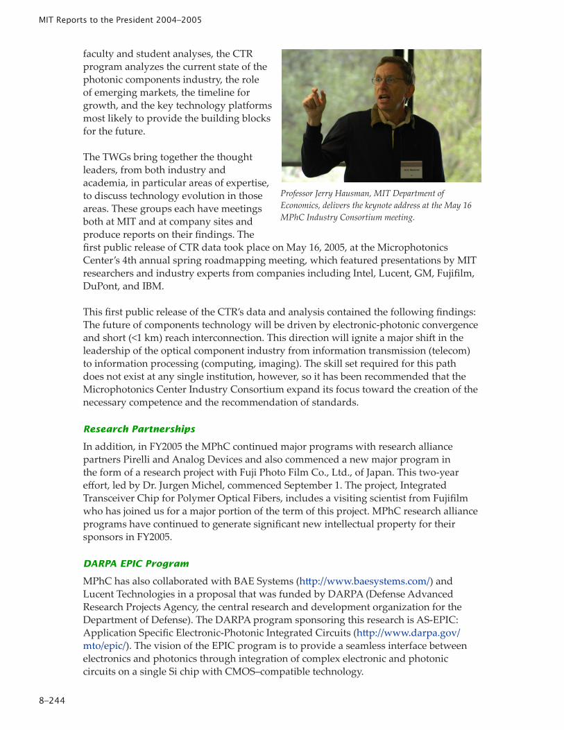
The TWGs bring together the thought leaders, from both industry and academia, in particular areas of expertise, to discuss technology evolution in those areas. These groups each have meetings both at MIT and at company sites and produce reports on their findings. The first public release of CTR data took place on May 16, 2005, at the Microphotonics Center’s 4th annual spring roadmapping meeting, which featured presentations by MIT researchers and industry experts from companies including Intel, Lucent, GM, Fujifilm, DuPont, and IBM.
This first public release of the CTR’s data and analysis contained the following findings: The future of components technology will be driven by electronic-photonic convergence and short (<1 km) reach interconnection. This direction will ignite a major shi� in the leadership of the optical component industry from information transmission (telecom) to information processing (computing, imaging). The skill set required for this path does not exist at any single institution, however, so it has been recommended that the Microphotonics Center Industry Consortium expand its focus toward the creation of the necessary competence and the recommendation of standards.
Research Partnerships
In addition, in FY2005 the MPhC continued major programs with research alliance partners Pirelli and Analog Devices and also commenced a new major program in the form of a research project with Fuji Photo Film Co., Ltd., of Japan. This two-year effort, led by Dr. Jurgen Michel, commenced September 1. The project, Integrated Transceiver Chip for Polymer Optical Fibers, includes a visiting scientist from Fujifilm who has joined us for a major portion of the term of this project. MPhC research alliance programs have continued to generate significant new intellectual property for their sponsors in FY2005.
DARPA EPIC Program
MPhC has also collaborated with BAE Systems (h�p://www.baesystems.com/) and Lucent Technologies in a proposal that was funded by DARPA (Defense Advanced Research Projects Agency, the central research and development organization for the Department of Defense). The DARPA program sponsoring this research is AS-EPIC: Application Specific Electronic-Photonic Integrated Circuits (h�p://www.darpa.gov/mto/epic/). The vision of the EPIC program is to provide a seamless interface between electronics and photonics through integration of complex electronic and photonic circuits on a single Si chip with CMOS–compatible technology.
Professor Jerry Hausman, MIT Department of Economics, delivers the keynote address at the May 16 MPhC Industry Consortium meeting.

Materials Processing Center/Microphotonics Center
8–245
Materials Research at MIT
Detailed summaries of research by MPC–affiliated faculty can be found in Materials Research at MIT, available in electronic format at our website. The 2005 edition will be posted to the site at the beginning of the fall semester.
Education Activities
One pillar of the Materials Processing Center is the education of the next generation of materials processing research scientists, engineers, and leaders. To this end, the MPC initiates programs to enhance the intellectual vitality of the materials processing community at MIT. We measure the value of these programs by the breadth of the materials arena they address, by the new and creative collaborations among faculty and students they catalyze, and by the degree of a�ention to the multidisciplinary—but at the same time fundamental—nature of the materials science, engineering, and processing they generate.
Seminars
We archive seminars, with the speakers’ assistance, on our web sitein the form of a PowerPoint presentation with audio track. In this way we hope to capture our seminars as an ongoing information resource to the community. For FY2006, seminars will be available live via eMeeting to anyone unable to join us physically on campus.
25th Anniversary Seminar Series
MPC is planning a special seminar series for the coming year, as part of the 25th Anniversary celebration.
Materials Unlimited Seminar Series
Now in its sixth year, the Materials Unlimited Seminar Series highlights the research of senior graduate students identified by faculty members as being among the best in MIT materials-related research. These seminars include a half-hour talk by the featured graduate student, followed by a half-hour panel discussion. Panelists are drawn from MIT and other university faculty and from companies with commercial interest in the topic. Seminars are well a�ended by a diverse audience of faculty, postdocs, graduate students, and undergraduates. The Materials Unlimited Seminar Series will continue during FY2006, with one seminar per semester.
Microphotonics Seminar Series
The MPhC sponsors a seminar series to educate faculty and students regarding science, technology, and commercial applications in this rapidly emerging field. This series is a key part of the value proposition of the center to its industry sponsors as well. A list of topics plus abstracts can be found via our web site.
Materials Day
Materials Day is an annual event, usually in the fall, that celebrates the MIT materials research community. It features a daylong workshop on a featured topic, followed by a graduate student/postdoc poster session. The next Materials Day is scheduled for October 11. The theme of the symposium, chaired by Professor Michael Rubner, director,
MIT Reports to the President 2004–2005
8–246
Center for Materials Science and Engineering, is “Interdisciplinary Research Groups at the Frontiers of Materials Science and Engineering.”
CMSE’s interdisciplinary research groups (IRGs) investigate fundamental scientific questions and pathways to reach significant technological goals that can only be properly explored in a collaborative, multidisciplinary mode. The four current IRGs include
• Microphotonic Materials and Structures• Electronic Transport in Mesoscopic Semiconductor and Magnetic Structures• Nanostructured Polymer Assemblies• Science and Engineering of Solid-State Portable Power Sources
Materials Day 2005 will feature both ongoing research and results to date of these efforts via both faculty presentations and an extensive poster session.
Summer Research Internship Program
The MPC and the Center for Materials Science and Engineering cosponsor and comanage the MPC–CMSE Summer Research Internship Program. This 10-week program brings outstanding juniors and seniors in science or engineering majors from academic institutions around the United States to MIT to work in the laboratories of participating faculty members.
The summer of 2005 brought 15 students a�ending from schools as far flung as Stanford University, Yale University, Case Western Reserve University, Oakwood College, Brigham Young University, and the University of Puerto Rico. These students worked with faculty from various departments on a wide variety of projects.
Outreach Activities
The second pillar of the MPC is its outreach to new (either MIT or MPC) faculty and researchers, as well as to the global materials community. MPC has a dozen visiting scientists from industry working within the center. The center is proactive in inviting faculty to participate in its activities, whether through our publications, educational programs, or research sponsorship.
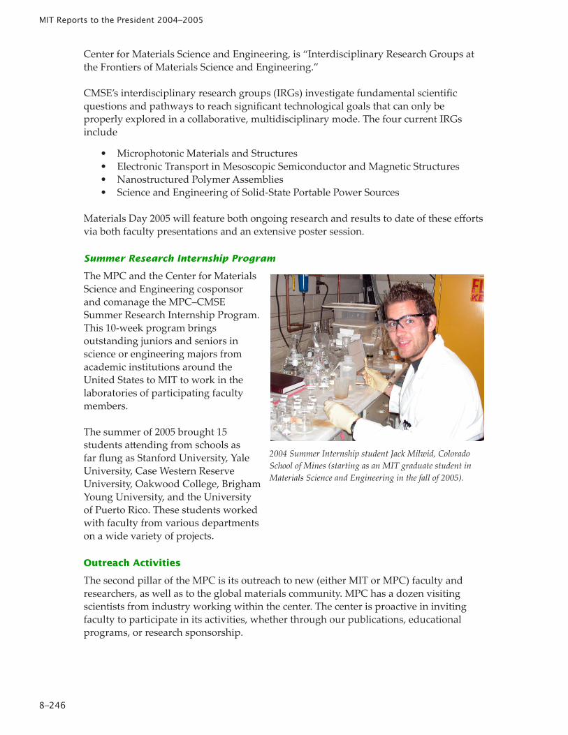
2004 Summer Internship student Jack Milwid, Colorado School of Mines (starting as an MIT graduate student in Materials Science and Engineering in the fall of 2005).
Materials Processing Center/Microphotonics Center
8–247
Industry
The MPC Industry Collegium maintained its full complement of activities and, simultaneously, the industrial support base of the Microphotonics Center grew in a recovering economy. Collegium membership currently exceeds 25 companies, domestic and international. We added several new collegium members during FY2005. The MphC Industry Consortium announced a new structure with expanded membership. It also maintained its relationship with the sponsors of its major research alliances, Pirelli and Analog Devices. MPhC also began a relationship with Fuji Photo Film Co. of Japan. Visiting industrial scientists affiliated with these programs are appointed through the MPC.
Information Management
The MPC produces several publications, brochures, conference booklets, and three web sites in pursuit of its outreach goals. One publication, Materials Research at MIT, is a digest of materials research performed at MIT by MPC–affiliated faculty and others during the previous calendar year. It provides a short summary of each project being researched by faculty members, along with a list of their personnel and publications. Materials Research at MIT 2005 will provide the reports of 70 faculty members. The 2005 research digest, produced together with the Center for Materials Science and Engineering (CMSE), was distributed entirely via the MPC web site. Information from our research digest is used by CMSE in its NSF reporting responsibilities, DMSE in its recruitment and placement of new graduate students, and the Industrial Liaison Program for its KnowledgeBase database.
The MPC’s newsle�er, the Industry Collegium Report, has transitioned to web-based news articles. During FY2004 and 2005 we performed extensive revamping of our web site’s appearance and functionality. The web is currently our main mode of information distribution to our MPhC Industry Consortium members, particularly for the Communications Technology Roadmap Project (h�p://mph-roadmap.mit.edu/).
The most important new project in MPC publications, in collaboration with CMSE, is the creation of a new website, Materials at MIT. As described earlier in this report, this site will provide a gateway to materials science and engineering activities across the MIT community. The first phase of this project concluded with the launch of the Materials at MIT beta site in March of 2005. A�er working with the site and collecting some feedback, a second design phase is under way.
The MPhC was proud to produce the Communications Technology Roadmap digest and CD, to be distributed in August 2005. These publications represent the culmination of four years of effort by the CTR team.
The MPC supports interdisciplinary research teams with secure web sites for data sharing, teleconferencing and videoconferencing facilities for meetings, and staff support for research project management.
MIT Reports to the President 2004–2005
8–248
Equipment and Facilities
We have completed work jointly with CMSE, DMSE, MTL, RLE, and MIT facilities to renovate lab space to create significant new materials processing capability on campus. All of this equipment was brought online in 2004, as anticipated. The Substrate Engineering Lab in Building 13 is led by Professor Eugene Fitzgerald and features a metal-organic chemical vapor deposition tool from Thomas Swan and an ultrahigh vacuum chemical vapor deposition tool from Unaxis. The Nanoprecision Deposition Laboratory in Building 38 is led by Professor Leslie Kolodzjieski and features a Veeco dual chamber molecular beam epitaxy tool and a Veeco ion beam deposition system. An Applied Materials plasma-enhanced dielectric deposition tool was installed in Room 39-ICL Microsystems Technology Laboratories for open use by the MIT community.
The renovation of the 1,063-square-foot Characterization Lab for Photonic Materials and Integrated Devices, located in Building 12, has also been completed. This renovation, originally estimated to cost $400,000, was accomplished under severe budget constraints for only $20,000. By combining equipment from faculty laboratories and buying like-new state-of-the-art equipment at auction, it was possible to reduce the cost of the renovation by 95 percent. Five years ago sequential characterization was unnecessary, but with the new facility it is possible to perform 200 to 300 measurements overnight. The equipment in the Characterization Lab includes the Newport AutoAlign Workstation, a measurement system for high-speed detectors and modulators, and the Waveguide Evaluation Systems I and II. Still under construction is a TOSA/ROSA evaluation system.
Personnel
The MPC/MPhC staff during FY2005 numbered nine, including the director, Professor Lionel Kimerling. In the spring of 2005, Trisha Montalbo accepted the position of program manager of the Communications Technology Roadmap. In March, Mindy Baughman assumed the role of program manager of the Microphotonics Center Industry Consortium.
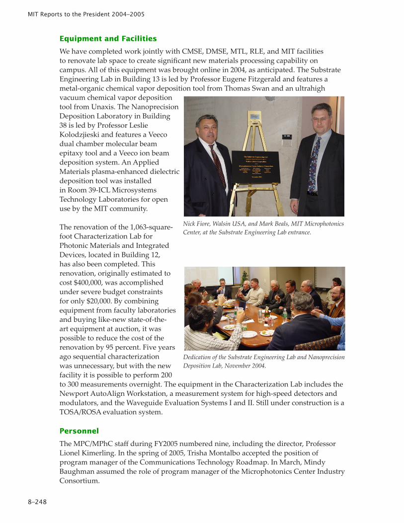
Dedication of the Substrate Engineering Lab and Nanoprecision Deposition Lab, November 2004.
Nick Fiore, Walsin USA, and Mark Beals, MIT Microphotonics Center, at the Substrate Engineering Lab entrance.
Materials Processing Center/Microphotonics Center
8–249
Outlook
The MPC/MPhC is expanding its collaborations with other materials-related centers across the campus to provide a common and guided gateway to the current maze of possibilities outside visitors face when approaching MIT with a materials problem. In addition, our moving closer to other centers—particularly CMSE—will create synergies both intellectually and administratively. Our strategy is to improve our position as an information resource for the campus community and portal for consortium/collegium member companies. Meanwhile, with our program sponsors and research alliance partners, we face the ongoing challenges of program and intellectual property management and are developing the tools and processes for meeting these challenges. We consider our key value to be our building of interdisciplinary faculty teams to develop new areas for intellectual activity and research.
Virtually every academic and industrial constituency is realizing the time for bo�om-up innovation is here. Materials innovation and process innovation, already interdisciplinary since the field’s inception, are at the center of even broader interdisciplinary activity. Specialists from the device and systems level experience difficulty in choosing and acquiring appropriate materials technologies and R&D pathways. Due to the new bo�om-up idea that system-level value can originate from atoms, molecules, and materials, there is a paucity of leaders who can comfortably and accurately plan “atoms-to-finance” visions. The emergence of vertically integrated thinkers on the revenue side (i.e., some traditional sources of research financing in government and industry) needs to be encouraged and placed on firmer pedagogical grounds.
The long-term strategic vision of the MPC must be to embrace these changes and create maximum opportunity for MPC students and professors. This requires MPC to continue to supply technology leadership and information consolidation to an even broader community. Traditionally, MPC has been an interface for industry to the MIT community. Today the MPC is becoming an interface for systems integrators (industrial and government) to gather information about bo�om-up opportunities in general. This is a significant shi� in role, and the MPC community is responding well. Recent programs have followed a new path in which the MPC is a consolidator of information and technology leadership not only across MIT, but across other universities, equipment suppliers, materials suppliers, and outsourced R&D contract facilities. Essentially, the trend appears to be the need for government and industry to have a “one-stop shop” for technology leadership in building system-level value through atoms, molecules, and solids.
The MPC must act as an intellectual leader in materials innovation and processing across the MIT community and the external community and interface with government and industrial systems integrators. The short-term plan is to continue building the relationship base to act as this central consolidator and leader in the materials community. In each sector of MPC research activity, system integrators must be identified and relationships established. This process in the defense sector is well under way, and the process has also started in the biomaterials/biotechnology area. With system integrator relationships growing, key community membership of individuals and resources outside the MIT community can also be folded into the MPC community.

MIT Reports to the President 2004–2005
8–250
There are five key trends for MPC over the next five years. The first—vanishing academic department boundaries—has resulted in dual appointments for some new faculty. Another key trend is a new sort of triangular industry-government-university partnership. More intellectual property creation, a third key trend, is related to the collaboration we help arrange. Industry expects more IP, so more collaboration means more IP creation. The application-rich nature of industry enables us to do what we do best—develop basic, fundamental research, then apply it when we get the opportunities. Other key trends are interdisciplinary research teams with vertical integration to applications and the materials innovation we see all around us in the 21st century.
One of the major challenges at MIT is the need for a be�er sense of community. The Materials Processing Center has provided, for the past quarter century, a successful means of achieving a be�er sense of community within the School of Engineering. Looking ahead, MPC anticipates that the next quarter century will be even more exciting than the first, as collaborative initiatives with other materials research organizations on and off campus take shape and take flight.
Lionel C. Kimerling Director Professor of Materials Science and Engineering
More information about the Materials Processing Center can be found online at h�p://mpc-web.mit.edu/.