materials - concordia universityusers.encs.concordia.ca/~mojtaba/elec...
TRANSCRIPT

Materials
• Almost all optoelectronic light source depend upon epitaxial crystal growth
techniques where a thin film (a few microns) of semiconductor alloys are
grown on single-crystal substrate; the film should have roughly the same
crystalline quality. It is necessary to make strain-free heterojunction with
good-quality substrate. The requirement of minimizing strain effects arises
from a desire to avoid interface states and to encourage long-term device
reliability, and this imposes a lattice-matching condition on the materials
used.

Schematic illustration of the the structure of a double heterojunction stripecontact laser diode
Oxide insulator
Stripe electrode
SubstrateElectrode
Active region where J > Jth.
(Emission region)
p-GaAs (Contacting layer)
n-GaAs (Substrate)
p-GaAs (Active layer)
Current
paths
L
W
Cleaved reflecting surfaceElliptical
laser
beam
p-AlxGa
1-xAs (Confining layer)
n-AlxGa
1-xAs (Confining layer)
12 3
Cleaved reflecting surface
Substrate
© 1999 S.O. Kasap, Optoelectronics (Prentice Hall)
Solid State Optoelectronic Devices
Optical Sources; Laser,
LED
Switches
Photodiodes
Photodetectors
Solar Cells

Materials
• The constraints of bandgap and lattice match force that more complex compound must be chosen.
These compounds include ternary (compounds that containing three elements) and quaternary
(consisting of four elements) semiconductors of the form AxB1-xCyD1-y; variation of x and y are
required by the need to adjust the band-gap energy (or desired wavelength) and for better lattice
matching. Quaternary crystals have more flexibility in that the band gap can be widely varied while
simultaneously keeping the lattice completely matched to a binary crystal substrate. The important
substrates that are available for the laser diode technology are GaAs, InP and GaP. A few
semiconductors and their alloys can match with these substrates. GaAs was the first material to
emit laser radiation, and its related to III-V compound alloys, are the most extensively studied
developed.

Materials
III-V semiconductors•Ternary Semiconductors; Mixture of binary-binary semiconductors; AxB1-xC; mole fraction, x, changes from 0 to 1(x will be adjusted for specific required wavelength). GaxAl1-xAs ; In0.53Ga0.47As; In0.52Al0.48As
-Vegard’s Law: The lattice constant of AxB1-xC varies linearly from the lattice constant of the semiconductor AC to that of the semiconductor BC.
-The bandgap energy changes as a quadratic function of x.
-The index of refraction changes as x changes.
•The above parameters cannot vary independently
•Quaternary Semiconductors; AxB1-xCyD1-y (x and y will be adjusted for specific wavelength and matching lattices).GaxIn1-xPyAs1-y ; (AlxGa1-x)yIn1-yP; AlxGa1-xAsySb1-y
2cxbxaEg

Materials
• II-VI Semiconductors
CdZnSe/ZnSe; visible blue lasers.Hard to dope p-type impurities at
concentration larger than 21018cm-3 (due to
self-compensation effect). Densities on this
order are required for laser operation.

Materials
• IV-VI semiconductors
PbSe; PbS; PbTe
• By changing the proportion of Pb atoms in these materials semiconductor changes from n- to p-type.
• Operate around 50 Ko
• PbTe/Pb1-xEuxSeyTe1-y operates at 174 Ko

Materials

Materials
• In the near infrared region, the most important and certainly the most
extensively characterized semiconductors are GaAs, AlAs and their
ternary derivatives AlxGa1-xAs.
• At longer wavelengths, the materials of importance are InP and ternary
and quaternary semiconductors lattice matched to InP. The smaller
band-gap materials are useful for application in the long wavelength
range.

Energy Band Structure of Semiconductors

Materials

0.2
0.4
0.6
0.8
1
1.2
1.4
1.6
1.8
2
2.2
2.4
2.6
0.54 0.55 0.56 0.57 0.58 0.59 0.6 0.61 0.62
Lattice constant, a (nm)
GaP
GaAs
InAs
InP
Direct bandgap
Indirect bandgap
In0.535Ga0.465AsX
Quaternary alloys
with direct bandgap
In1-xGaxAs
Quaternary alloys
with indirect bandgap
Eg (eV)
Bandgap energy Eg and lattice constant a for various III-V alloys ofGaP, GaAs, InP and InAs. A line represents a ternary alloy formed withcompounds from the end points of the line. Solid lines are for directbandgap alloys whereas dashed lines for indirect bandgap alloys.Regions between lines represent quaternary alloys. The line from X toInP represents quaternary alloys In1-xGaxAs1-yPy made fromIn0.535Ga0.465As and InP which are lattice matched to InP.
© 1999 S.O. Kasap, Optoelectronics (Prentice Hall)

Example:
III-V compound semiconductors in optoelectronics Figure in the
previous page represents the bandgap Eg and the lattice parameter a
in the quarternary III-V alloy system. A line joining two points
represents the changes in Eg and a with composition in a ternary alloy
composed of the compounds at the ends of that line. For example,
starting at GaAs point, Eg = 1.42 eV and a = 0.565 nm, Eg decreases
and a increases as GaAs is alloyed with InAs and we move along the
line joining GaAs to InAs. Eventually at InAs, Eg = 0.35 eV and a =
0.606 nm. Point X in Figure 3Q6 is composed of InAs and GaAs and
it is the ternary alloy InxGa1-xAs. It has Eg = 0.7 eV and a = 0.587
nm which is the same a as that for InP. InxGa1-xAs at X is therefore
lattice matched to InP and can hence be grown on an InP substrate
without creating defects at the interface.

Further, InxGa1-xAs at X can be alloyed with InP to obtain a quarternary alloy
InxGa1-xAsyP1-y whose properties lie on the line joining X and InP and therefore
all have the same lattice parameter as InP but different bandgap. Layers of
InxGa1-xAsyP1-y with composition between X and InP can be grown epitaxially
on an InP substrate by various techniques such as liquid phase epitaxy (LPE) or
molecular beam expitaxy (MBE) .
The shaded area between the solid lines represents the possible values
of Eg and a for the quarternary III-V alloy system in which the bandgap is direct
and hence suitable for direct recombination.
The compositions of the quarternary alloy lattice matched to InP follow
the line from X to InP.
a Given that the InxGa1-xAs at X is In0.535Ga0.465As show that quarternary
alloys In1-xGaxAsyP1-y are lattice matched to InP when y = 2.15x.
b The bandgap energy Eg, in eV for InxGa1-xAsyP1-y lattice matched to
InP is given by the empirical relation,
Eg (eV) = 1.35 - 0.72y + 0.12 y2
Find the composition of the quarternary alloy suitable for an emitter
operating at 1.55 mm.

Materials
y = 2.2 x
Basic Semiconductor Luminescent Diode Structures
LEDs (Light Emitting Diode)
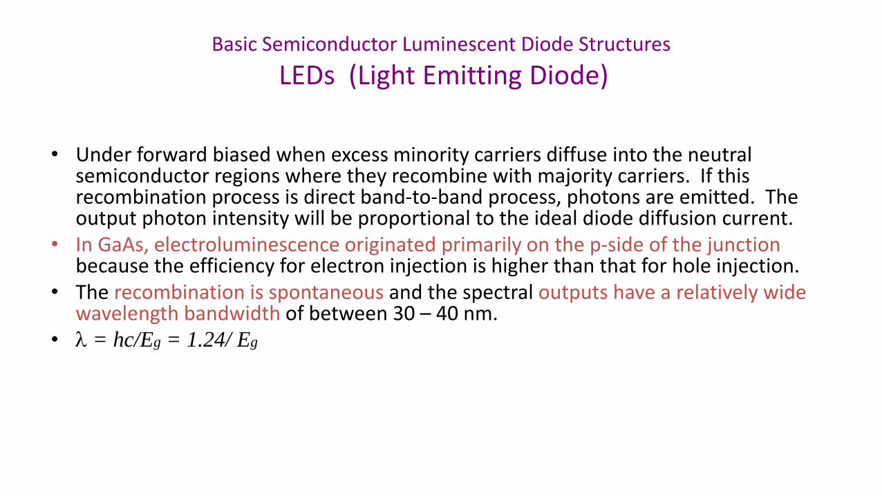
• Under forward biased when excess minority carriers diffuse into the neutral semiconductor regions where they recombine with majority carriers. If this recombination process is direct band-to-band process, photons are emitted. The output photon intensity will be proportional to the ideal diode diffusion current.
• In GaAs, electroluminescence originated primarily on the p-side of the junctionbecause the efficiency for electron injection is higher than that for hole injection.
• The recombination is spontaneous and the spectral outputs have a relatively wide wavelength bandwidth of between 30 – 40 nm.
• = hc/Eg = 1.24/ Eg

Photon Emission in Semiconductors
Light output
Insulator (oxide)p
n+ Epit axial layer
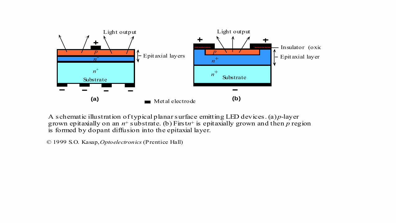
A schematic illustration of typical planar surface emitting LED devices . (a) p-layergrown epitaxially on an n+ substrate. (b) Firs t n+ is epitaxially grown and then p regionis formed by dopant diffusion into the epitaxial layer.
Light output
pEpit axial layers
(a) (b)
n+
Substrate Substrate
n+
n+
Met al electrode
© 1999 S.O. Kasap, Optoelectronics (Prentice Hall)

Basic Semiconductor Luminescent Diode Structures

Basic Semiconductor Luminescent Diode Structures
2 eV
2 eVeVo
Holes in VB
Electrons in CB
1.4 eVNo bias
With
forward
bias
Ec
EvEc
Ev
EFEF
(a)
(b)
(c)
(d)
pn+ p
Ec
GaAs AlGaAsAlGaAs
ppn+
~ 0.2 m
AlGaAsAlGaAs
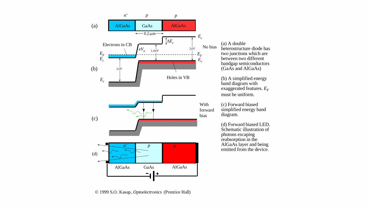
(a) A doubleheterostructure diode hastwo junctions which arebetween two differentbandgap semiconductors(GaAs and AlGaAs)
(b) A simplified energyband diagram withexaggerated features. EF
must be uniform.
(c) Forward biasedsimplified energy banddiagram.
(d) Forward biased LED.Schematic illustration ofphotons escapingreabsorption in theAlGaAs layer and beingemitted from the device.
© 1999 S.O. Kasap, Optoelectronics (Prentice Hall)
GaAs

Ec
Ev
E1
E1
h = E1 – E
1
E
In single quantum well (SQW) lasers electrons areinjected by the forward current into the thin GaAslayer which serves as the active layer. Populationinversion between E1 and E1 is reached even with a
small forward current which results in stimulatedemissions.
© 1999 S.O. Kasap, Optoelectronics (Prentice Hall)

0.4 0.5 0.6 0.7 0.8 0.9 1.0 1.1 1.2 1.3 1.4 1.5 1.6
Blu
e
Gre
en
Ora
nge
Yel
low
Red
1.7
Infrared
Vio
let
GaA
s
GaA
s 0.5
5P0.4
5
GaAs1-yPy
InP
In0.1
4Ga 0
.86A
s
In1-xGaxAs1-yPy
AlxGa1-xAs
x = 0.43G
aP(N
)
GaS
b
Indirect
bandgap
InG
aNS
iC(A
l)
In0.7G
a 0.3A
s 0.6
6P0.3
4
In0.5
7Ga 0
.43A
s 0.9
5P0.0
5
Free space wavelength coverage by different LED materials from the visible spectrum to theinfrared including wavelengths used in optical communications. Hatched region and dashedlines are indirect Eg materials.
In0.49AlxGa0.51-xP
© 1999 S.O. Kasap, Optoelectronics (Prentice Hall)


E
Ec
Ev
Carrier concentration
per unit energy
Electrons in CB
Holes in VB
h
1
0
Eg
h
h
h
CB
VB
Relative intensity
1
0
h
Relative intensity
(a) (b) (c) (d)
Eg + kBT
(2.5-3)kBT
1/2kBT
Eg
1 2 3
2kBT
(a) Energy band diagram with possible recombination paths. (b) Energy distribution ofelectrons in the CB and holes in the VB. The highest electron concentration is (1/2)kBT above
Ec . (c) The relative light intensity as a function of photon energy based on (b). (d) Relativeintensity as a function of wavelength in the output spectrum based on (b) and (c).
© 1999 S.O. Kasap, Optoelectronics (Prentice Hall)
LED Characteristics

V
2
1
(c)
0 20 40
I (mA)0
(a)
600 650 700
0
0.5
1.0
Relative
intensity
24 nm
655nm
(b)
0 20 40I (mA)0
Relative light intensity
(a) A typical output spectrum (relative intensity vs wavelength) from a red GaAsP LED.(b) Typical output light power vs. forward current. (c) Typical I-V characteristics of ared LED. The turn-on voltage is around 1.5V.
© 1999 S.O. Kasap, Optoelectronics (Prentice Hall)
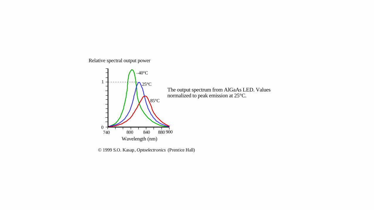
800 900
–40°C
25°C
85°C
0
1
740
Relative spectral output power
840 880
Wavelength (nm)
The output spectrum from AlGaAs LED. Valuesnormalized to peak emission at 25°C.
© 1999 S.O. Kasap, Optoelectronics (Prentice Hall)
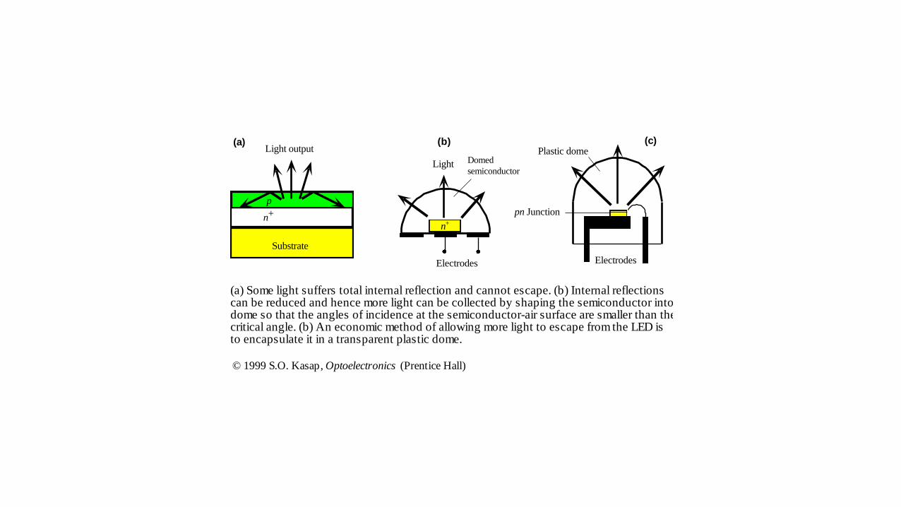
Light output
p
Electrodes
Light
Plastic dome
Electrodes
Domed
semiconductor
pn Junction
(a) (b) (c)
n+
n+
(a) Some light suffers total internal reflection and cannot escape. (b) Internal reflectionscan be reduced and hence more light can be collected by shaping the semiconductor into adome so that the angles of incidence at the semiconductor-air surface are smaller than thecritical angle. (b) An economic method of allowing more light to escape from the LED isto encapsulate it in a transparent plastic dome.
Substrate
© 1999 S.O. Kasap, Optoelectronics (Prentice Hall)
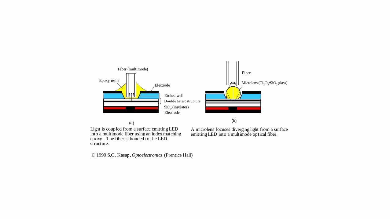
Electrode
SiO2 (insulator)
Electrode
Fiber (multimode)
Epoxy resin
Etched well
Double heterostructure
Light is coupled from a surface emitting LEDinto a multimode fiber using an index matchingepoxy. The fiber is bonded to the LEDstructure.
(a)
Fiber
A microlens focuses diverging light from a surfaceemitting LED into a multimode optical fiber.
Microlens (Ti2O3:SiO2 glass)
(b)
© 1999 S.O. Kasap, Optoelectronics (Prentice Hall)
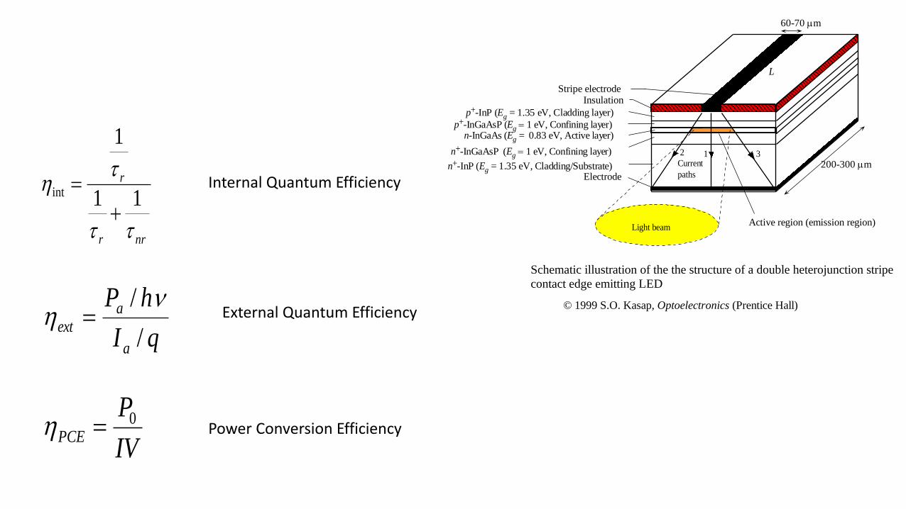
Schematic illustration of the the structure of a double heterojunction stripe
contact edge emitting LED
InsulationStripe electrode
SubstrateElectrode
Active region (emission region)
p+-InP (Eg = 1.35 eV, Cladding layer)
n+-InP (Eg = 1.35 eV, Cladding/Substrate)
n-InGaAs (Eg = 0.83 eV, Active layer)
Current
paths
L
60-70 m
Light beam
p+-InGaAsP (Eg 1 eV, Confining layer)
n+-InGaAsP (Eg 1 eV, Confining layer) 12 3
200-300 m
© 1999 S.O. Kasap, Optoelectronics (Prentice Hall)
qI
hP
a
aext
/
/
IV
PPCE
0
nrr
r
11
1
int
Internal Quantum Efficiency
External Quantum Efficiency
Power Conversion Efficiency

Active layer Barrier layer
Ec
Ev
E
A multiple quantum well (MQW) structure.Electrons are injected by the forward currentinto active layers which are quantum wells.
© 1999 S.O. Kasap, Optoelectronics (Prentice Hall)

Multimode fiberLens
(a)
ELED
Active layer
Light from an edge emitting LED is coupled into a fiber typically by using a lens or aGRIN rod lens.
GRIN-rod lens
(b)
Single mode fiberELED
© 1999 S.O. Kasap, Optoelectronics (Prentice Hall)

LASERS
• The sensitivity of most photosensitive material is greatly increased at wave-length < 0.7 m; thus, a laser with a short wave-length is desired for such applications as printers and image processing.
• The sensitivity of the human eye range between the wavelengths of 0.4 and 0.8m and the highest sensitivity occur at 0.555m or green so it is important to develop laser in this spectral regime for visual applications.
• Lasers with wavelength between 0.8 – 1.6 m are used in optical communication systems.

LASERS
• The semiconductor laser diode is a forward bias p-n junction. The structure appears to be similar to the LED as far as the electron and holes are concerned, but it is quite different from the point of view of the photons. Electrons and holes are injected into an active region by forward biasing the laser diode. At low injection,these electrons and holes recombine (radiative) via the spontaneous process to emit photons. However, the laser structure is so designed that at higher injections the emission process occurs by stimulated emission. As we will discuss, the stimulated emission process provides spectral purity to the photon output, provides coherent photons, and offers high-speed performance.
• The exact output spectrum from the laser diode depends both on the nature of the optical cavity and the optical gain versus wavelength characteristics.
• Lasing radiation is only obtained when optical gain in the medium can overcome the photon loss from the cavity, which requires the diode current I to exceed a threshold value Ith and gop>gth
• Laser-quality crystals are obtained only with lattice mismatches <0.01% relative to the substrate.

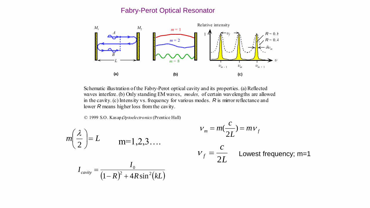
A
B
L
M1 M2 m = 1
m = 2
m = 8
Relative intensity
m
m m + 1m - 1
(a) (b) (c)
R ~ 0.4
R ~ 0.81 f
Schematic illus tration of the Fabry-Perot optical cavity and its properties. (a) Reflectedwaves interfere. (b) Only standing EM waves, modes, of certain wavelengths are allowed
in the cavity. (c) Intens ity vs. frequency for various modes. R is mirror reflectance and
lower R means higher loss from the cavity.
© 1999 S.O. Kasap, Optoelectronics (Prentice Hall)
Lm
2
m=1,2,3….
kLRR
IIcavity 22
0
sin41
fm mL
cm )
2(
L
cf
2 Lowest frequency; m=1
Fabry-Perot Optical Resonator

L
m
m - 1
Fabry-Perot etalon
Partially reflecting plates
Output lightInput light
Transmitted light
Transmitted light through a Fabry-Perot optical cavity.
© 1999 S.O. Kasap, Optoelectronics (Prentice Hall)
2
0
max1 R
II
kLRR
RII incidentdtransmitte 22
2
sin41
1
R
RF
1
2/1Finesse measures the loss in
the cavity, F increases as loss
decreases
It is maximum when kL=mπ
m
fF
=ratio of the mode separation to
spectral width

LASER Diode Modes of Threshold Conditions
Lasing Conditions:
Population Inversion
Fabry-Perot cavity
gain (of one or several modes) > optical loss
zhvhvg
eIzI
)(
)0()(
I – optical field intensity
g – gain coefficient in F.P. cavity
- effective absorption coefficient
Γ – optical field confinement factor. (the fraction of
optical power in the active layer)
In one round trip i.e. z = 2L gain
should be > loss for lasing;
During this round trip only R1 &
R2 fractions of optical radiation
are reflected from the two laser
ends 1 & 2.
2
21
21
nn
nnR

LASER Diode Modes of Threshold Conditions
From the laser conditions: ,)()2( oILI
)0()0()2(
_
2
21 IeRRILIgL
21
2 1_
RRe
gL
21
_ 1ln2
RRgL
endthRRL
g _
21
_ 1ln
2
1
Lasing threshold is the point at
which the optical gain is equal to the
total loss αt
endtthg _
thth Jgg β– is constant and depends on the
specific device construction.
Thus the gain

Laser Diode Rate Equations
Rate Equations govern the interaction of photons and electrons in
the active region.
ph
spRBndt
d
= stimulated emission + spontaneous emission - photon loss
Bnn
qd
J
dt
dn
sp
= injection - spontaneous recombination - stimulated emission
(shows variation of electron concentration n).
Variation of photon concentration:
The relationship between optical output and the diode drive current:
d - is the depth of carrier-confinement region
B - is a coefficient (Einstein’s) describing the strength of
the optical absorption and emission interactions,;
Rsp - is rate of spontaneous emission into the lasing mode;
τph
– is the photon lifetime;
τsp
– is the spontaneous recombination lifetime;
J – is the injection current density;

Laser Diode Rate Equations
Solving the above Equations for a steady-state condition yields an
expression for the output power.
0dt
d0
dt
dnSteady-state => and
n must exceed a threshold value nth in order for Φ to increase.
In other words J needs to exceed Jth in steady-state condition, when the number
of photons Φ=0.
sp
thth n
qd
J
No stimulating emission
This expression defines the current required to sustain an excess
electron density in the laser when spontaneous emission is the only
decay mechanism.

Laser Diode Rate Equations
0
0
qd
JnBn
RBn
sp
thsth
ph
sspsth
Now, under steady-state condition at the lasing threshold:
Фs is the steady-state photon density.
0qd
JnR
sp
th
ph
ssp
phph
sp
thphsps
qd
JnR
qd
Jn th
sp
th
phspth
ph
s RJJqd
# of photon resulting from stimulated emission
Adding these two equations: but
The power from the first term is generally concentrated in one or few modes;
The second term generates many modes, in order of 108 modes.

Laser Diode Rate Equations
To find the optical power P0:
c
nLt time for photons to cross cavity length L.
s2
1- is the part travels to right or left (toward output
face)
R is part of the photons reflected and 1-R
part will escape the facet
t
Rhvvolume
Ps
12
1
0
th
phJJ
qn
RWhcP
2
)1(2
0
W is the width of active layer

Laser Characteristics
P0
J
Jth
nth
P0 lasing output power ≡ Фs
Threshold
population
inversion
n

Typical output optical power vs. diode current (I) characteristics and the correspondingoutput spectrum of a laser diode.
Laser
LaserOptical Power
Optical Power
I0
LEDOptical Power
Ith
Spontaneous
emission
Stimulated
emission
Optical Power
© 1999 S.O. Kasap, Optoelectronics (Prentice Hall)

Laser CharacteristicsResonant Frequency
mL 22 /2 n
mLn
2
22
c
nLv2
nLm
2
So:
n
Lm
2
This states that the cavity resonates (i.e. a standing wave pattern exists
within it) when an integer number m of λ/2 spans the region between the
mirrors. Depending on the laser structures, any number of freq. can satisfy
1&)0()2( 2 LjeILI
Thus some lasers are single - & some are multi-modes.
The relationship between gain & freq. can be assumed
to have Gaussian form:
2
20
2)0()(
egg
where λ0 is the wavelength at the center of spectrum;
σ is the spectrum width of gain & maximum g(0) is
proportional to the population inversion.
Remember that inside the
optical cavity for
zero phase difference :
12 Lje ; ;

Laser CharacteristicsSpacing between the modes:
mvc
Lnm
2 L
n
m
2
1
21 mv
c
Lnm
Lnm
Ln
m
Ln
m
Lnm
2
2
1
22 2
2
122
1 vc
Lnvv
c
Lnmm
Ln
cv
2
vc 2
cv
cv
LnLn
cc
22
2
2
m
Ln2or

Laser CharacteristicsInternal & External Quantum Efficiency
Quantum Efficiency (QE) = # of photons generated for each EHP
injected into the semiconductor junction a measure of the efficiency
of the electron-to-photon conversion process.
If photons are counted at the junction region, QE is called internal
QE (int
), which depends on the materials of the active junction and
the neighboring regions. For GaAs int
= 65% to 100%.
If photons are counted outside the semiconductor diode QE is
external QE(ext
).
Consider an optical cavity of length L , thickness W and width S. Defining a
threshold gain gth as the optical gain needed to balance the total power loss,
due to various losses in the cavity, and the power transmission through the
mirrors .
Laser CharacteristicsInternal & External Quantum Efficiency
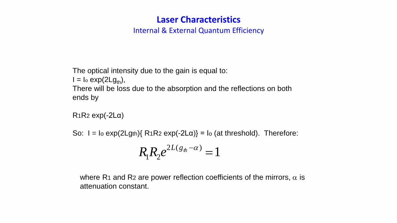
The optical intensity due to the gain is equal to:
I = Io exp(2Lgth),
There will be loss due to the absorption and the reflections on both
ends by
R1R2 exp(-2Lα)
So: I = Io exp(2Lgth){ R1R2 exp(-2Lα)} = Io (at threshold). Therefore:
1)(2
21 thgL
eRR
where R1 and R2 are power reflection coefficients of the mirrors, is
attenuation constant.

Laser CharacteristicsInternal & External Quantum Efficiency
21
1ln
2
1
RRLg th
g is gain constant of the active
region and is roughly
proportional to current density (g
= J). is a constant.
21
1ln
2
1)/1(
RRLJ th
By measuring Jth, , L, R1 and R2 one
can calculate (dependent upon the
materials and the junction structure).
The ratio of the power radiated
through mirrors to the total power
generated by the semiconductor
junction istotal
ra
P
P
RRL
RRL
21
21
1ln
2
1
1ln
2
1

nrr
r
RR
R
int
q
IRR nrr
q
IR
q
I
Rr
rintint
h
PRr
int
hq
IP intint
th
thext
g
g
)(int
Internal efficiencyI is the current in diode
Pint is internal optical power
External effeciency

Laser CharacteristicsInternal & External Quantum Efficiency
Therefore ext= int(Pra/Ptotal) which can be determined
experimentally from PI characteristic.
For a given Ia (in PI curve current at point a) the number of
electrons injected into the active area/sec = Ia /q and the number
of photons emitted /second = Pa /h
qI
hP
a
aext
/
/
qI
hP
b
bext
/
/
I
P
h
q
hII
PPq
ba
baext
)(
)(
i.e. ext is proportional to slope of PI curve in the region of I >
Ith.
th
extII
P
h
q
If we choose Ib = Ith , Pb0 and
h Eg and h/q = Eg /q gives voltage
across the junction in volts.

Laser CharacteristicsPower Efficiency
At dc or low frequency the equivalent circuit to a LASER diode may be
viewed as an ideal diode in series with rs.
Therefore the power efficiency =
p =(optical power output)/ (dc electrical power input)
sg
prIqEI
P2)/(
extthIIq
hP
)(
sg
gthext
prIqEI
qEII2)/(
/)(

LElectrode
Current
GaAs
GaAsn+
p+
Cleaved surface mirror
Electrode
Active region(stimulated emission region)
A schematic illustration of a GaAs homojunction laserdiode. The cleaved surfaces act as reflecting mirrors.
L
© 1999 S.O. Kasap, Optoelectronics (Prentice Hall)
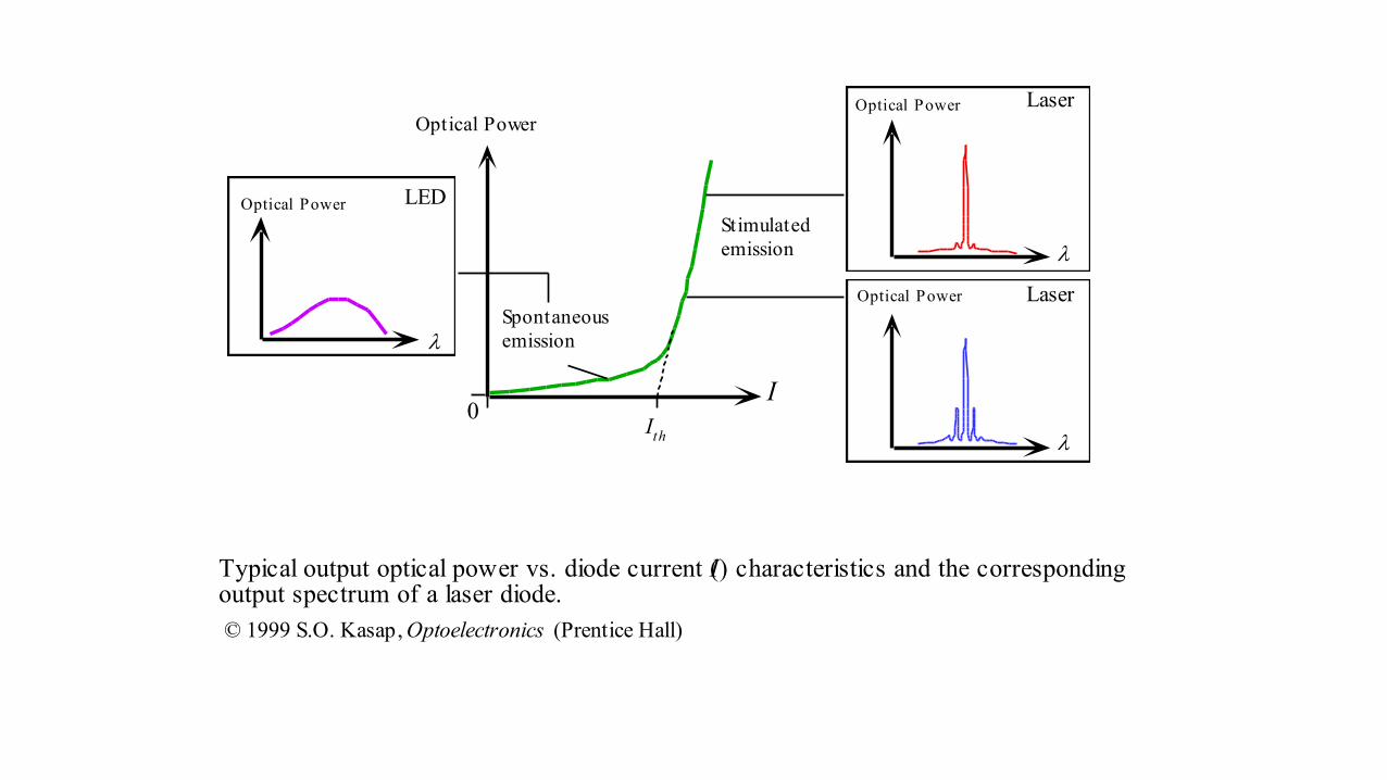
Typical output optical power vs. diode current (I) characteristics and the correspondingoutput spectrum of a laser diode.
Laser
LaserOptical Power
Optical Power
I0
LEDOptical Power
Ith
Spontaneous
emission
Stimulated
emission
Optical Power
© 1999 S.O. Kasap, Optoelectronics (Prentice Hall)

Refractiveindex
Photondensity
Active
region
n ~ 5%
2 eV
Holes in VB
Electrons in CB
AlGaAsAlGaAs
1.4 eV
Ec
Ev
Ec
Ev
(a)
(b)
pn p
Ec
(a) A doubleheterostructure diode hastwo junctions which arebetween two differentbandgap semiconductors(GaAs and AlGaAs).
2 eV
(b) Simplified energyband diagram under alarge forward bias.Lasing recombinationtakes place in the p-GaAs layer, theactive layer
(~0.1 m)
(c) Higher bandgapmaterials have alower refractiveindex
(d) AlGaAs layersprovide lateral opticalconfinement.
(c)
(d)
© 1999 S.O. Kasap, Optoelectronics (Prentice Hall)
GaAs

Schematic illustration of the the structure of a double heterojunction stripecontact laser diode
Oxide insulator
Stripe electrode
SubstrateElectrode
Active region where J > Jth.
(Emission region)
p-GaAs (Contacting layer)
n-GaAs (Substrate)
p-GaAs (Active layer)
Current
paths
L
W
Cleaved reflecting surfaceElliptical
laser
beam
p-AlxGa
1-xAs (Confining layer)
n-AlxGa
1-xAs (Confining layer)
12 3
Cleaved reflecting surface
Substrate
© 1999 S.O. Kasap, Optoelectronics (Prentice Hall)

Oxide insulation
n-AlGaAs
p+-AlGaAs (Contacting layer)
n-GaAs (Substrate)
p-GaAs (Active layer)
n-AlGaAs (Confining layer)
p-AlGaAs (Confining layer)
Schematic illustration of the cross sectional structure of a buriedheterostructure laser diode.
Electrode
© 1999 S.O. Kasap, Optoelectronics (Prentice Hall)

Height, HWidth W
Length, L
The laser cavity definitions and the output laser beamcharacteristics.
Fabry-Perot cavity
Dielectric mirror
Diffraction
limited laser
beam
© 1999 S.O. Kasap, Optoelectronics (Prentice Hall)
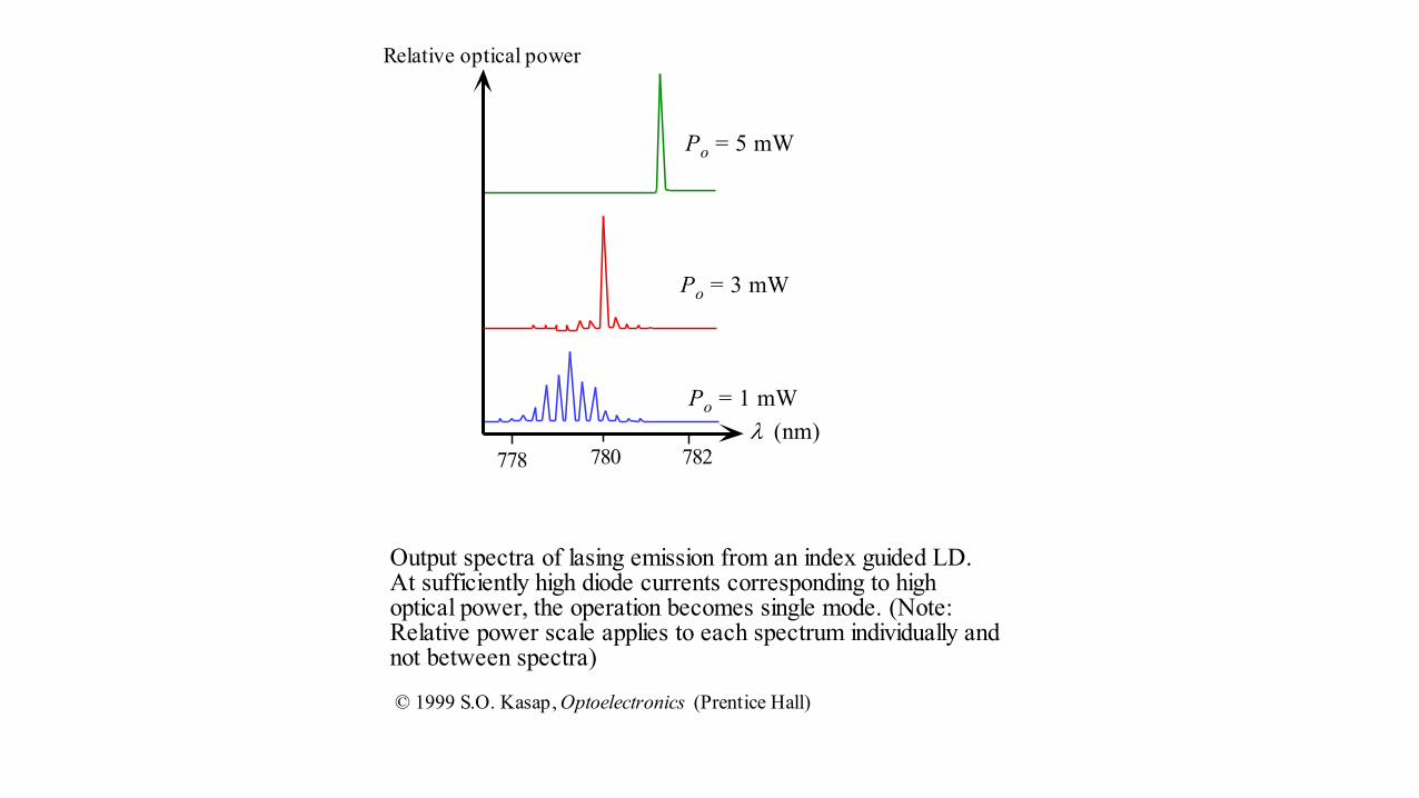
778 780 782
Po = 1 mW
Po = 5 mW
Relative optical power
(nm)
Po = 3 mW
Output spectra of lasing emission from an index guided LD.At sufficiently high diode currents corresponding to highoptical power, the operation becomes single mode. (Note:Relative power scale applies to each spectrum individually andnot between spectra)
© 1999 S.O. Kasap, Optoelectronics (Prentice Hall)

Typical optical power output vs. forward currentfor a LED and a laser diode.
Current0
Light powerLaser diode
LED
100 mA50 mA
5 mW
10 mW
© 1999 S.O. Kasap, Optoelectronics (Prentice Hall)

Corrugated
dielectric structure
Distributed Bragg
reflector
(a) (b)
A
B
q(B/2n) =
Active layer
(a) Distributed Bragg reflection (DBR) laser principle. (b) Partially reflected wavesat the corrugations can only constitute a reflected wave when the wavelengthsatisfies the Bragg condition. Reflected waves A and B interfere constructive when
q(B/2n) = .
© 1999 S.O. Kasap, Optoelectronics (Prentice Hall)

Active layer
Corrugated grating
Guiding layer
(a)
(a) Distributed feedback (DFB) laser structure. (b) Ideal lasing emission output. (c)Typical output spectrum from a DFB laser.
Optical power
(nm)
0.1 nm
Ideal lasing emission
B(b) (c)
© 1999 S.O. Kasap, Optoelectronics (Prentice Hall)

Fiber Bragg grating
Bowei Zhang, Presentation for the
Degree of Master of Applied Science
Department of Electrical
and Computer Engineering
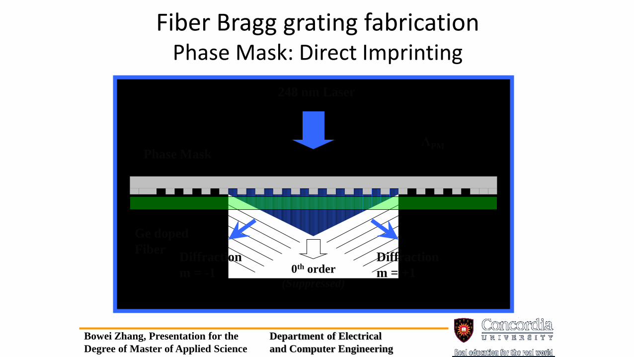
Fiber Bragg grating fabricationPhase Mask: Direct Imprinting
Bowei Zhang, Presentation for the
Degree of Master of Applied Science
Department of Electrical
and Computer Engineering
0th order
(Suppressed)
Diffraction
m = -1
Diffraction
m = +1
Phase MaskΛPM
Ge doped
Fiber
248 nm Laser

Active
layer
L D
(a)
Cleaved-coupled-cavity (C3) laser
Cavity Modes
In L
In D
In both
L and D
(b)
© 1999 S.O. Kasap, Optoelectronics (Prentice Hall)

A quantum well (QW) device. (a) Schematic illustrat ion of a quantum well (QW) structure in which athin layer of GaAs is sandwiched between two wider bandgap semiconductors (AlGaAs). (b) Theconduction electrons in the GaAs layer are confined (by ² Ec) in the x-direction to a small length d so
that their energy is quantized. (c) The density of stat es of a two-dimensional QW. The density of statesis constant at each quantized energy level.
AlGaAs AlGaAs
GaAs
y
z
x
d
Ec
Ev
d
E1
E2
E3
g(E)Density of states
E
BulkQW
n = 1
Eg2Eg1
E n = 2² Ec
BulkQW
² Ev
(a) (b) (c)
Dy
Dz
© 1999 S.O. Kasap, Optoelectronics (Prentice Hall)

Ec
Ev
E1
E1
h = E1 – E
1
E
In single quantum well (SQW) lasers electrons areinjected by the forward current into the thin GaAslayer which serves as the active layer. Populationinversion between E1 and E1 is reached even with a
small forward current which results in stimulatedemissions.
© 1999 S.O. Kasap, Optoelectronics (Prentice Hall)

Active layer Barrier layer
Ec
Ev
E
A multiple quantum well (MQW) structure.Electrons are injected by the forward currentinto active layers which are quantum wells.
© 1999 S.O. Kasap, Optoelectronics (Prentice Hall)