material selection & technology processes for 5g systems
TRANSCRIPT

Material Selection & Technology Processes for 5G
Systems
Vitaly Bensman
Senior Process Engineer at Eltek Ltd.
17 June 2020

The Mobile Wireless Communication Technology
1
10,000Mbit/sec 1,000Mbit/sec 42Mbit/sec 0.064Mbit/sec 0.0024Mbit/sec
Era of IoT Era of mobile Internet
Brought mobile data
Introduced digital voice
Delivered analog voice
2020 2010 2000 1990 1980
0G 1946
[2]

5G is the 5th generation mobile network. It will take a much larger role than previous generations.
5G will elevate the mobile network to not only interconnect people, but also interconnect and control machines, objects, and devices.
What is 5G ?
2
5G benefits: deliver multi-Gbps
peak rates ultra-low latency massive capacity
[7]
5G and PCB Materials
Overall, 5G is a complex system and PCB is necessary in every constituent hardware part.
The main development directions of PCB in the 5G era are multilayer applications, high frequency, high speed, high density, rigid-flex and mixed high and low frequencies.
Traditional epoxy resin copper clad laminate (CCL) cannot meet the high frequency requirement of 5G environments.
In the 5G era millimeter-wave band between 30 GHz and 300 GHz will be put into use to improve the wireless data capacity.[4]
The PTFE CCL is an excellent dielectric material with a low dielectric constant and minimal dielectric loss and has many applications. It can be widely used in mobile communication equipment, radio receivers, transfer devices, base station antennae, and consumers electronics.
3

Selection PCB Materials for 5G
4
Choosing a circuit material for a high-frequency PCB is generally a tradeoff, often between price and performance.
But PCB materials are also selected by two key factors:
how well they meet the needs of an end-use application
what kind of effort is required to fabricate a desired circuit with a particular material. [3]
Choosing Materials Based on Circuit Fabrication Issues
5
A number of different mechanical processes are required as part of high-frequency PCB fabrication. In general, the most critical of these would be:
Multilayer Lamination
Drilling
Plated-Through-Hole (PTH) Preparation
Assembly

Choosing Materials Based on Circuit Fabrication Issues
6
Drilling and PTH Preparation
The drilling process is typically concerned with creating clean
holes, which will later be metalized to form VIA-holes for electrical connections from one conductive layer to another.
Some concerns with the drilling process include:
Smear - smearing can be lethal to PCB fabrication using a PTFE based material, since there is no way to remove the smear.
Burring- can lead to reduce hole diameter and could be a trigger to mechanical and electrical falls in thermal cycles.
Fracturing of the material - fracturing can be fatal for some of the nonwoven glass and hydrocarbon materials.

Choosing Materials Based on Circuit Fabrication Issues
7
Multilayer Lamination and Assembly
Fabricating multilayer PCBs presents many challenges.
One is the fact that dissimilar materials are often being bonded together, and these dissimilar materials can have properties which complicate drilling and PTH preparation processes.
Also, a mismatch between certain material properties, such as coefficient of thermal expansion (CTE), can lead to reliability problems when the circuit is thermally stressed during assembly.
A goal of the material selection process is to find a good combination of circuit materials for a multilayer PCB which enable practical fabrication processing while also meeting end-use requirements. [3]

Choosing Materials Based on Circuit Fabrication Issues
8
Designers and fabricators have many choices of materials used to bond together the copper-clad laminates that ultimately form a multilayer PCB. [3]
Re-melting Temperature [ºC]
Preparation for PTH
Lamination Temperature [ºC]
Df Dk Bonding Materials
337 Special 390 0.0009 2.2 Glass Microfiber Reinforced PTFE
271 Special 296 0.0010 2.1 FEP (Fluorinated
ethylene propylene)
337 Special 371 0.0013 3.00 Ceramic-filled PTFE,
Dk=3
337 Special 371 0.0020 6.15 Ceramic-filled PTFE,
Dk=6
337 Special 371 0.0023 10.80 Ceramic-filled PTFE,
Dk=10
271 Special 290 0.0025 2.90 LCP
176 Special 218 0.0030 2.30 3001
N/A Standard 176 0.0040 3.90 Thermoset Hydrocarbo
N/A Standard 182 0.0180 4.50 FR-4

Choosing Materials Based on Circuit Fabrication Issues
9
The greatest concern during PCB assembly is due to the effects of thermal stress from soldering.
In terms of circuit materials, effects from thermal stress can typically be projected by comparing the CTE values for different materials. [3]
In general, a circuit material with a lower CTE will be more robust and handle the thermal stress better than a material with a higher overall CTE.

Choosing Materials Based on Circuit Fabrication Issues
10
Thermal Conductivity
The heat generated by the 5G PCB is often related to insertion loss. Basically , a circuit with higher insertion loss will generate more heat.
Using a high-frequency materials that has a high thermal conductivity can be very beneficial to the thermal management 5G application. [8]
Water Absorption
50 %
Thermal Conductivi
ty W/(m•K)
(50°C)
Coefficient of Thermal
Expansion -55° to 288°C
ppm/°C (X/Y/Z)
Thermal Coefficient of
Dk -50°C to 150°C
ppm/°C
Df @ 10 GHz
Dk, @ 10 GHz
Product
0.04 0.50 10/12/34 -9 0.0023 2.98±0.04 CLTE™
Woven Glass Reinforced PTFE
0.03 0.42 8/8/30 NA 0.0017 3.05±0.10 RO1200™
PTFE Ceramic Woven Glass Reinforced
0.04 0.50 17/16/25 -3 0.0010 3.00±0.04 RO3003™
PTFE Ceramic
0.02 0.20 31/48/237 -125 0.0009 2.20±0.02 RT/duroid 5880
PTFE Random Glass Fiber
0.05 0.69 10/12/32 +50 0.0037 3.48±0.05 RO4350B™
Hydrocarbon Ceramic Woven Glass

Environment Changes Affect on Dk and Df
11 Dk vs. ºC
Data from Rogers Corporation ®

High Electrical Performance Compare to Other Lamination Methods
12
Pri
ce
[6]
The fabricating PTFE-based multilayer circuits can require special handling of the circuit materials for optimum results. [1]
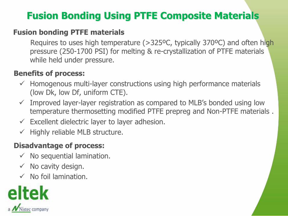
Fusion Bonding Using PTFE Composite Materials
13
Fusion bonding PTFE materials
Requires to uses high temperature (>325ºC, typically 370ºC) and often high pressure (250-1700 PSI) for melting & re-crystallization of PTFE materials while held under pressure.
Benefits of process:
Homogenous multi-layer constructions using high performance materials (low Dk, low Df, uniform CTE).
Improved layer-layer registration as compared to MLB’s bonded using low temperature thermosetting modified PTFE prepreg and Non-PTFE materials .
Excellent dielectric layer to layer adhesion.
Highly reliable MLB structure.
Disadvantage of process:
No sequential lamination.
No cavity design.
No foil lamination.
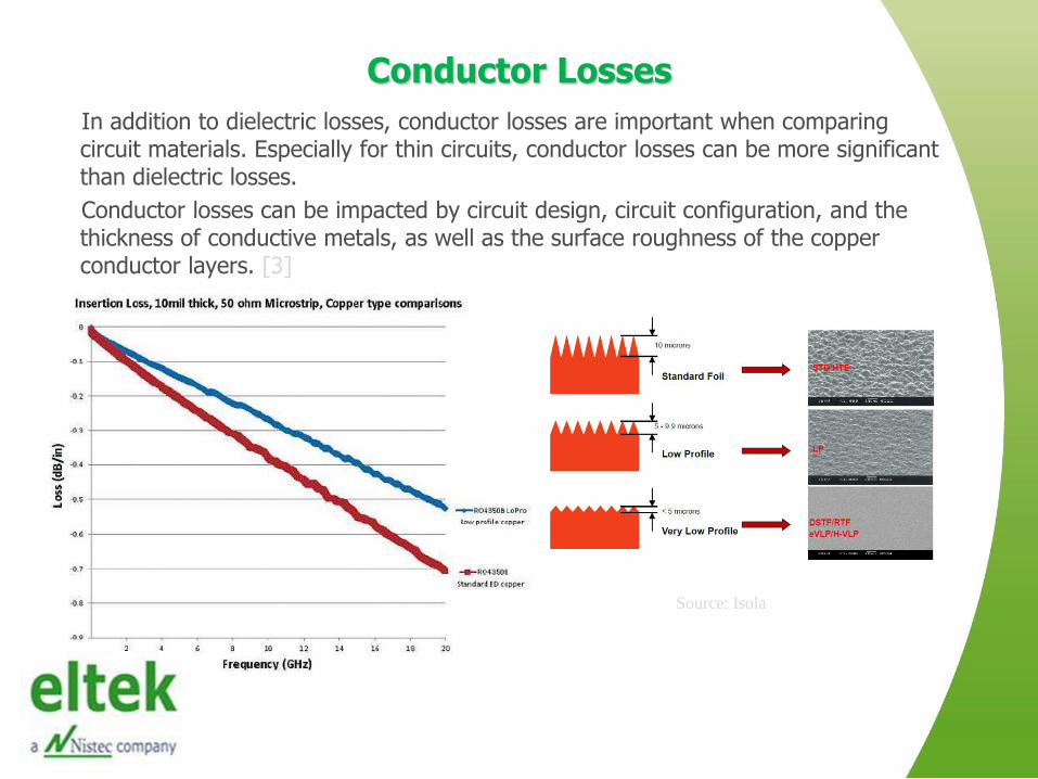
Conductor Losses
14
In addition to dielectric losses, conductor losses are important when comparing circuit materials. Especially for thin circuits, conductor losses can be more significant than dielectric losses.
Conductor losses can be impacted by circuit design, circuit configuration, and the thickness of conductive metals, as well as the surface roughness of the copper conductor layers. [3]
Source: Isola

Fusion Bonding Using PTFE Composite Materials
Direct Bonding:
Bonding together pressed (densified) cores (require to use high pressure as 1000-1700 PSI)
Requires use of fully etched surfaces against copper-pattern inner-layer (prohibited vertical stacking of copper on opposing layers)
May require fully etched “spacer” core between opposing copper layers
15

Fusion Bonding Using PTFE Composite Materials
Bondply Bonding:
Uses undensified (“unpressed”) layers of RT/duroid 6002™ or RO3000® materials between opposing core layers
Traditional core/adhesive/core MLB stack-up (Bondply layers used similar to core layers during fusion bond process. Bondply ply bonding make better fill and therefore require lower pressure such 400-500 PSI)
16
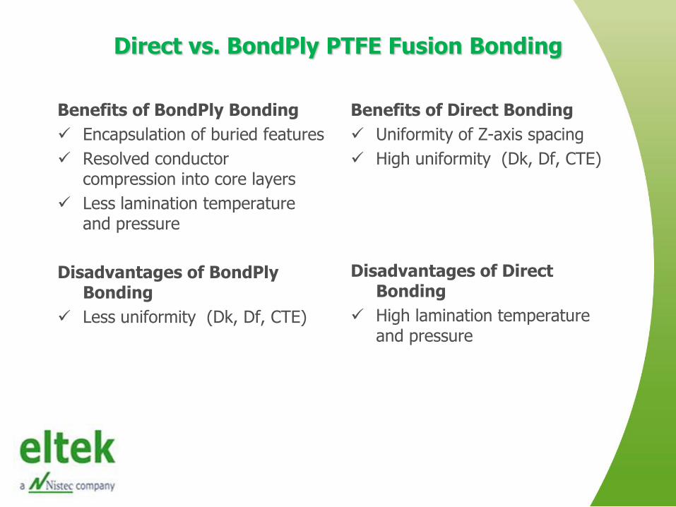
Direct vs. BondPly PTFE Fusion Bonding
Benefits of BondPly Bonding
Encapsulation of buried features
Resolved conductor compression into core layers
Less lamination temperature and pressure
Disadvantages of BondPly Bonding
Less uniformity (Dk, Df, CTE)
Benefits of Direct Bonding
Uniformity of Z-axis spacing
High uniformity (Dk, Df, CTE)
Disadvantages of Direct Bonding
High lamination temperature and pressure
17

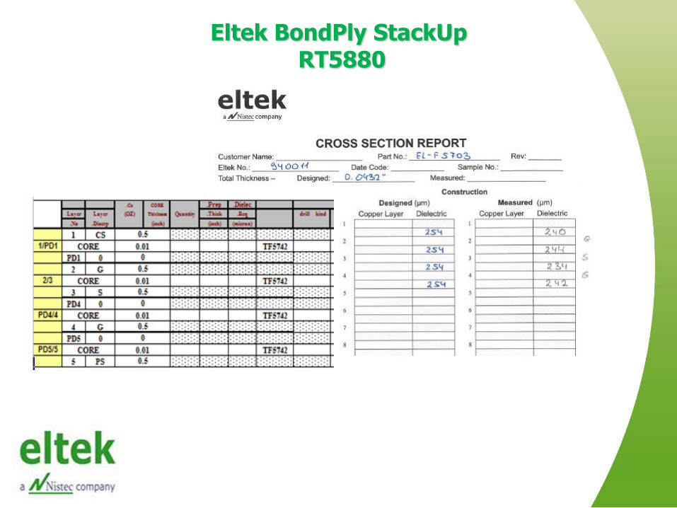
Eltek BondPly StackUp RT6002+RO3003
18
RT6002 @10GHz Dk 2.94±0.04; Df 0.0012
RO3003@10GHz Dk 3.00±0.04; Df 0.0010
Press temperature 370ºC
Pressure 500 PSI

Eltek BondPly StackUp RT6002+RO3003
19

Registration RT6002+RO3003
20

Registration RT6002+RO3003
21
Good centering position
Good layer to layer registration

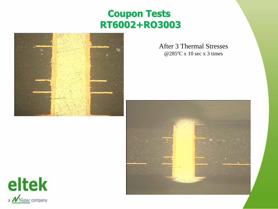
Coupon Tests RT6002+RO3003
22
After Press Core RT6002
Bond Ply RO3003
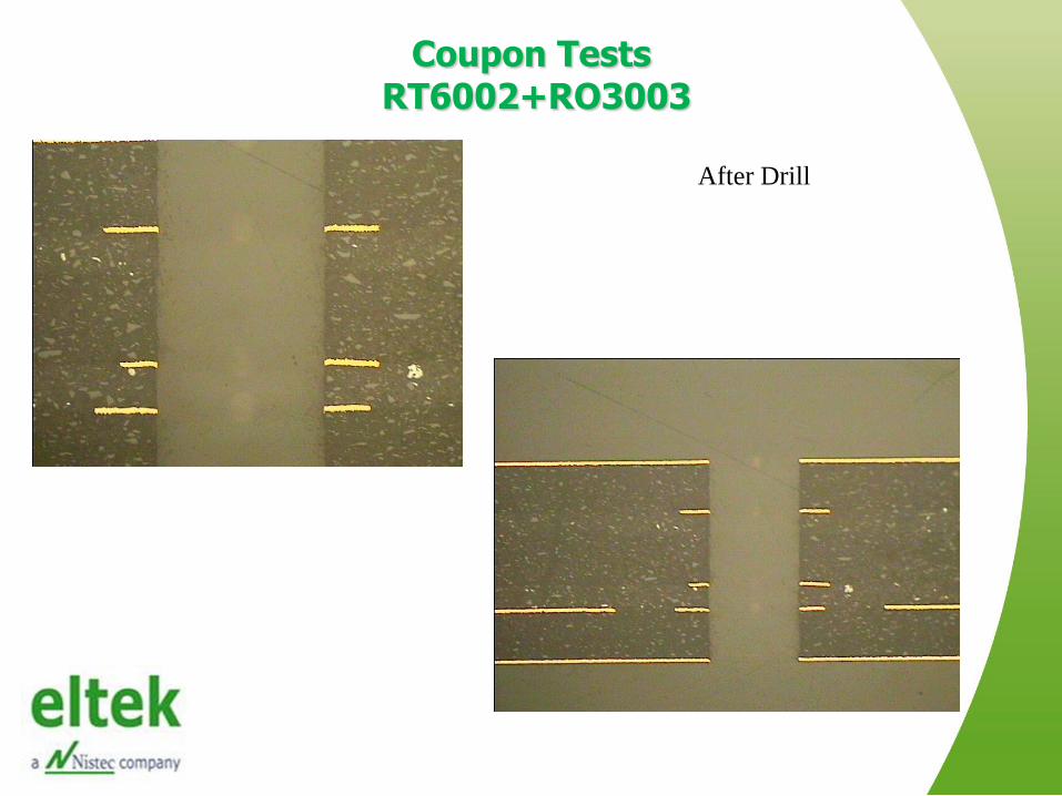
Coupon Tests RT6002+RO3003
23
After Drill
Coupon Tests RT6002+RO3003
24
After 3 Thermal Stresses @285ºC x 10 sec x 3 times

Coupon Tests RT6002+RO3003
25
After 6 Thermal Stresses @285ºC x 10 sec x 6 times

Eltek Direct Bonding StackUp RT5880
26
RT5880 @10GHz Dk 2.20±0.02; Df 0.0009
Press temperature 370ºC
Pressure 500 PSI
Eltek BondPly StackUp RT5880
27

Registration RT5880
28

Registration RT5880
29
Good centering position
Good layer to layer registration

Coupon Tests RT5880
30
After Press

Coupon Tests RT5880
31
After Cu Plating

Coupon Tests RT5880
32
After 3 Thermal Stresses @285ºC x 10 sec x 3 times

Coupon Tests RT5880
33
After 6 Thermal Stresses @285ºC x 10 sec x 6 times
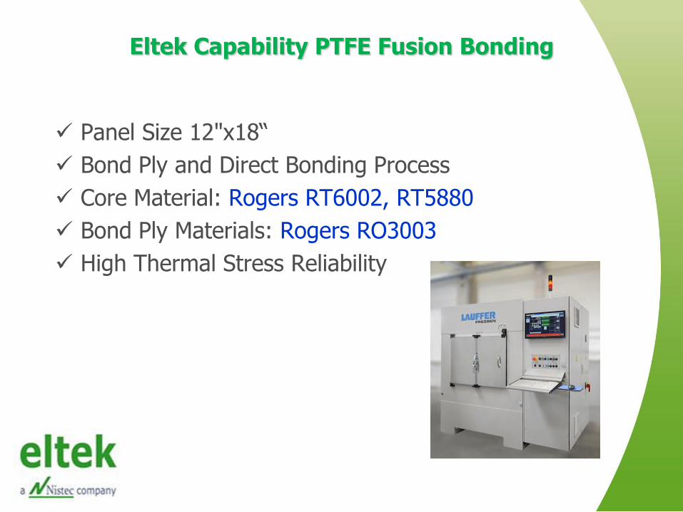
Eltek Capability PTFE Fusion Bonding
Panel Size 12"x18“
Bond Ply and Direct Bonding Process
Core Material: Rogers RT6002, RT5880
Bond Ply Materials: Rogers RO3003
High Thermal Stress Reliability
34
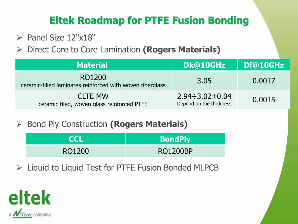
Eltek Roadmap for PTFE Fusion Bonding
Panel Size 12"x18“
Direct Core to Core Lamination (Rogers Materials)
Bond Ply Construction (Rogers Materials)
Liquid to Liquid Test for PTFE Fusion Bonded MLPCB
35
Df@10GHz Dk@10GHz Material
0.0017 3.05 RO1200 ceramic-filled laminates reinforced with woven fiberglass
0.0015 2.94÷3.02±0.04 Depend on the thickness
CLTE MW ceramic filed, woven glass reinforced PTFE
BondPly CCL
RO1200BP RO1200
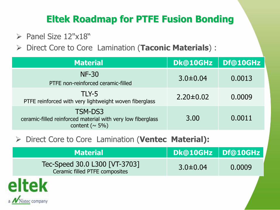
Eltek Roadmap for PTFE Fusion Bonding
Panel Size 12"x18“
Direct Core to Core Lamination (Taconic Materials) :
36
Df@10GHz Dk@10GHz Material
0.0013 3.0±0.04 NF-30
PTFE non-reinforced ceramic-filled
0.0009 2.20±0.02 TLY-5 PTFE reinforced with very lightweight woven fiberglass
0.0011 3.00 TSM-DS3
ceramic-filled reinforced material with very low fiberglass content (~ 5%)
Df@10GHz Dk@10GHz Material
0.0009 3.0±0.04 Tec-Speed 30.0 L300 [VT-3703] Ceramic filled PTFE composites
Direct Core to Core Lamination (Ventec Material):
37
Sources of Information
1. www.microwavejournal.com/blogs/1-rog-blog/post/20670-fusion-bonding-forms-reliable-multilayer-circuits.
2. https://www.linkedin.com/pulse/mobile-wireless-communication-technology-journey-0g-mutabazi
3. HTTPS://WWW.EDN.COM/SELECTING-PCBMATERIALS-FOR-HIGH-FREQUENCY-APPLICATIONS
4. Copper Clad Laminate for High Frequency Printed-circuit Board in 5G era. Shuchang Feng.
University of York 2018.
5. Opportunities for High Frequency Materials in 5G and the IoT. Art Aguayo Rogers Corp., Chandler,
Ariz.
6. Optimizing PCB Performance and Cost through Lamination. Judy Warner. Chris Savalia.
Transline Technology Incorporated.
7. www.samsung.com
8. Material Choices for 5G PCB Applications. John Coonrod, Rogers Corporation.
Fusion Bonding Using Rogers PTFE Composite Materials. Rogers Corporation®
http://all4-pcb.us/lauffer/
38