material characterisation technique transmission electron ... · the use of optical microscope...
TRANSCRIPT

MATERIAL CHARACTERISATION TECHNIQUE
“TRANSMISSION ELECTRON MICROSCOPE”
Under Guidance of:
Prof. M.S. Bobji
Submitted by:
Nitin Kumar (09266)
Uttiya Mukherjee (09372)
Deep Shekhar Dewangan (09437)

CONTENTS
1. INTRODUCTION
2. WORKING PRINCIPLE
3. CONSTRUCTION
4. SAMPLE PREPARATION
5. CHEMICAL ANALYSIS BY EDS
6. ELECTRON SCATTERING: FROM DIFFUSION
TO DIFFRACTION
7. LIMITATIONS
8. MODIFICATIONS
9. CONCLUSION
10. REFERENCES

Introduction
The use of optical microscope limited the ability to resolve an object because of it’s
wavelength. TEM stands for Transmission Electron Microscopy was technique developed to
obtain magnification and hence details of a specimen, to a much better level than the
conventional optical microscopes. In TEM a beam of electrons is passed through an ultra-thin
specimen interacting with the specimen as it passes through. When electrons are accelerated
up to high energy levels (few hundreds keV) and focused on a material, they can scatter or
backscatter elastically or inelastically, or produce many interactions, source of different
signals such as X-rays, Auger electrons or light. Some of them are used in transmission
electron microscopy (TEM). An image is formed from the interaction of the electrons
transmitted through the specimen; the image is magnified and focused onto an imaging
device, such as a fluorescent screen, on a layer of photographic film, or to be detected by a
sensor such as a CCD camera.
The probable interaction between an electron and a specimen is given as below
The development of TEM took into consideration the quantum mechanical behaviour of
electron. The interaction of electron with the material was obtained due to the inherent nature
of electron which is a quantum mechanical object. Since the electrons have both wave and
particle nature and the de Broglie wavelength of electrons are significantly smaller than that
of light and so they have higher resolution capability. This enables the instrument's user to
examine fine detail—even as small as a single column of atoms, which is tens of thousands
times smaller than the smallest resolvable object in a light microscope. TEM forms a major
analysis method in a range of scientific fields, in both physical and biological sciences. TEMs
find application in cancer research, virology, materials science as well
as pollution, nanotechnology, and semiconductor research.
The major purpose of this project is to comprehensively cover the aspects of TEM. The
history behind successful development of first TEM is described next.

Working Principle
TEM works like a slide projector. A projector shines a beam of light which transmits through
the slide. The patterns painted on the slide only allow certain parts of the light beam to pass
through. Thus the transmitted beam replicates the patterns on the slide, forming an enlarged
image of the slide when falling on the screen.
TEMs work the same way except that they shine a beam of electrons (like the light in a slide
projector) through the specimen (like the slide). However, in TEM, the transmission of
electron beam is highly dependent on the properties of material being examined. Such
properties include density, composition, etc. For example, porous material will allow more
electrons to pass through while dense material will allow less. As a result, a specimen with a
non-uniform density can be examined by this technique. Whatever part is transmitted is
projected onto a phosphor screen for the user to see.
Construction

1) ELECTRON SOURCE (GUN):-
The first and basic part of the transmission electron microscope is the source of
electrons. It is usually a V-shaped filament made of LaB6 or W (tungsten) that is
wreathed with Wehnelt electrode (Wehnelt Cap). Due to negative potential of the
electrode, the electrons are emitted from a small area of the filament (point source). A
point source is important because it emits monochromatic electrons (with similar
energy).
In this, a positive electrical potential is applied to the anode, and the filament
(cathode) is heated until a stream of electrons is produced. The electrons are
accelerated by the positive potential down the column, and because of the negative
potential of cap, all electrons are repelled toward the optic axis. A collection of
electrons occurs in the space between the
Filament tip and Cap , which is called a space charge. Those electrons at the bottom of
the space charge (nearest to the anode) can exit the gun area through the small (<1
mm) hole in the Wehnelt Cap and then move down the column to be later used in
imaging.
2) CONDENSER LENS:- The stream of the electron from the electron gun is then focussed to a small, thin,
coherent beam by the use of condenser lenses.
The first lens determines the “spot size”; the general size range of the final spot that
strikes the sample.
The second lens actually changes the size of the spot on the sample.

3) CONDENSER APERTURE:- A condenser aperture is a thin disk or strip of metal with a small circular through-hole.
It is used to restrict the electron beams and filter out unwanted scattered electrons
before image formation.
4) SAMPLE: - The beam from the condenser aperture strikes the sample and the electron-sample
interaction takes place in three different ways. One is unscattered electrons
(transmitted beam), elastically scattered electrons (diffracted beam) and inelastically
scattered electrons.
5) OBJECTIVE LENS: -
The main function of the objective lens is to focuses the transmitted electron from the
sample into an image.
6) OBJECTIVE APERTURE:- Objective aperture enhances the contrast by blocking out high-angle diffracted
electrons.
7) SELECTED APERTURE:- It enables the user to examine the periodic diffraction of electron by ordered
arrangements of atoms in the sample.
8) PROJECTOR LENS:- The projector lens are used to expand the beam onto the phosphor screen.
9) SCREEN:- Imaging systems in a TEM consists of a phosphor screen, which may be made of fine
(10-100 micro meter) particulate zinc sulphide, for direct observation by the operator.
10) IMAGE PATTERN:- The image strikes the phosphor screen and light is generated, allowing the users to see
the image.
The darker areas of the image represent those areas of the sample that fewer electrons
are transmitted.
The lighter areas of the image represent those areas of the sample that more electrons
were transmitted.

Sample Preparation
The TEM sample should be thin (due to the absorption of the electron in the material),
so special care must be taken while cutting a thin slice of the metal so that the
specimen is not deformed during its preparation. This is because plastic deformation
can introduce unwanted structural defects in the microstructure that are visible in
TEM images. The various techniques are:-
a) SPARK CUTTER: - In this, electric discharge between a wire and the specimen
are used to cut the metal by removing small particles of metal from the surface of the
specimen.
b) FOCUSED ION BEAM (FIB):- A thin slice of the sample was cut by an ion
beam on a scanning ion microscope. The main advantage of this method is that it
allows for selective thinning at desired locations by cutting trenchies in the sample.
c) TEM SAMPLE PREPARATION OF AMCs:-

For AMCs, the following mechanical method is used: TEM foil specimens are prepared by
mechanical dimpling down to 20 μm, followed by argon ion milling on a Gatan Duo-Mill
machine, operating at an accelerating voltage of 5 kV and 10° incidence angle, with a liquid
nitrogen cooling stage to avoid sample heating and
Micro structural changes associated with the annealing effect. Such effects are generally
Experienced on first samples prepared on an ion mill without cooling stage (PIPS), resulting
in an unexpected and substantial coarsening of the precipitation state.
Chemical Analyses by EDS
The first step in phase identification before the analysis of the diffraction patterns is a
chemical analysis that can been done in a TEM microscope by X-rays energy dispersive
spectrometry EDS, or electron energy loss spectrometry EELS. In addition to many other
advantages such as the possibility of obtaining information on the chemical bonding and its
good spatial resolution, EELS is particularly appropriated for light elements (Z < ZAl), but
the identification of the chemical elements and the interpretation of the spectra are not as
straightforward as in EDS which remains a quick method for identifying and quantifying the
elements due to a user-friendly software.
Inelastic interactions between electrons and matter give different kinds of signals secondary
electrons, Auger electrons, X-rays, light and lattice vibrations. The X-ray energy corresponds
to a difference between two energy levels of the electron cloud of an atom. Since these levels
are quantified, the X-ray energy spectrum represents the signature
of the atom. The X-rays are detected by a semi-conductor and processed by a
detector protected by a ultrathin window and cooled at liquid nitrogen temperature
to avoid the thermal noise and the diffusion of the dopant in the semi-conductor. An EDS
spectrum is constituted by a background produced by the Bremsstrahlung X-rays and by
peaks characteristic to the chemical elements of the material.

Electron Scattering: From Diffusion to Diffraction
Diffusion
The electrons are quantum relativistic particles, by consequence their behaviour is
described by the Dirac equation which time independent Schrodinger equation of classic
quantum mechanic (with relativist corrections in the mass of the electron) constitutes a good
approximation . Neglecting the interactions between the electrons, the equation for an
electron before its interaction with the crystal is
,where is is the wave function associated to the electron and k the wave vector of the
electron which is linked to the tension of acceleration U by
The solution to the Schrodinger equation is a plane wave equation (non-localisation plane of
the electron) given by
During the interaction of the electron with the crystal the equation is
, where V(r) is the potential of the crystal. This differential equation can be expressed as an
integral form in the entire volume of the crystal by using the Green’s function which is
given by
The new equation formed is called the diffusion equation and is given by
where k is vector respecting |k| = |k(0)|. With this equation, one can see that the crystal
potential in r’ makes diffuse the electron wave in the k direction by the intermediate of a
spherical wave and a transmission factor given by (2πme/h2)V(r). This is closely akin to the
optical Huygens approach and its general Kirchhoff’s formulation . This equation can
be solved with some approximations on the form of the electron wave function under the
integral (Born approximations).
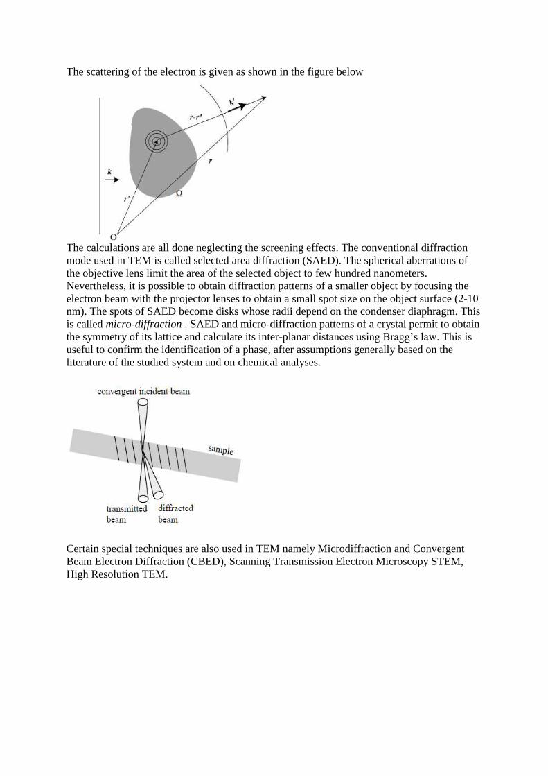
The scattering of the electron is given as shown in the figure below
The calculations are all done neglecting the screening effects. The conventional diffraction
mode used in TEM is called selected area diffraction (SAED). The spherical aberrations of
the objective lens limit the area of the selected object to few hundred nanometers.
Nevertheless, it is possible to obtain diffraction patterns of a smaller object by focusing the
electron beam with the projector lenses to obtain a small spot size on the object surface (2-10
nm). The spots of SAED become disks whose radii depend on the condenser diaphragm. This
is called micro-diffraction . SAED and micro-diffraction patterns of a crystal permit to obtain
the symmetry of its lattice and calculate its inter-planar distances using Bragg’s law. This is
useful to confirm the identification of a phase, after assumptions generally based on the
literature of the studied system and on chemical analyses.
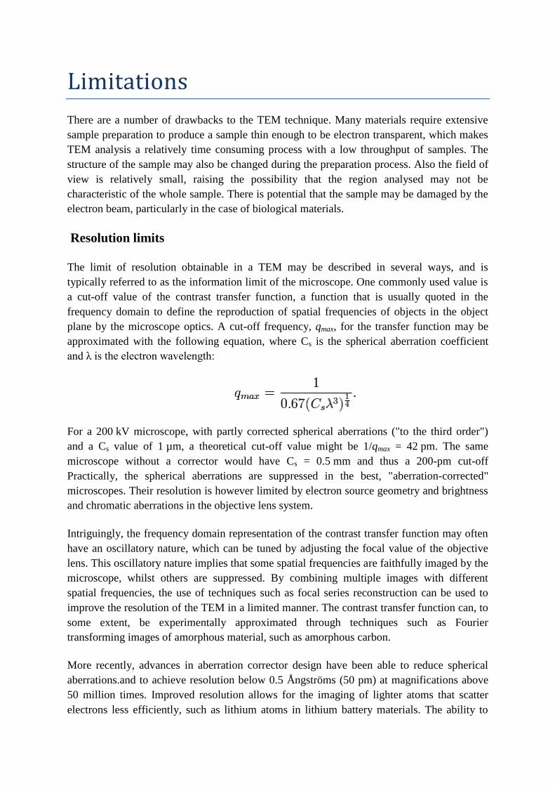
Certain special techniques are also used in TEM namely Microdiffraction and Convergent
Beam Electron Diffraction (CBED), Scanning Transmission Electron Microscopy STEM,
High Resolution TEM.
Limitations
There are a number of drawbacks to the TEM technique. Many materials require extensive
sample preparation to produce a sample thin enough to be electron transparent, which makes
TEM analysis a relatively time consuming process with a low throughput of samples. The
structure of the sample may also be changed during the preparation process. Also the field of
view is relatively small, raising the possibility that the region analysed may not be
characteristic of the whole sample. There is potential that the sample may be damaged by the
electron beam, particularly in the case of biological materials.
Resolution limits
The limit of resolution obtainable in a TEM may be described in several ways, and is
typically referred to as the information limit of the microscope. One commonly used value is
a cut-off value of the contrast transfer function, a function that is usually quoted in the
frequency domain to define the reproduction of spatial frequencies of objects in the object
plane by the microscope optics. A cut-off frequency, qmax, for the transfer function may be
approximated with the following equation, where Cs is the spherical aberration coefficient
and λ is the electron wavelength:
For a 200 kV microscope, with partly corrected spherical aberrations ("to the third order")
and a Cs value of 1 µm, a theoretical cut-off value might be 1/qmax = 42 pm. The same
microscope without a corrector would have Cs = 0.5 mm and thus a 200-pm cut-off
Practically, the spherical aberrations are suppressed in the best, "aberration-corrected"
microscopes. Their resolution is however limited by electron source geometry and brightness
and chromatic aberrations in the objective lens system.
Intriguingly, the frequency domain representation of the contrast transfer function may often
have an oscillatory nature, which can be tuned by adjusting the focal value of the objective
lens. This oscillatory nature implies that some spatial frequencies are faithfully imaged by the
microscope, whilst others are suppressed. By combining multiple images with different
spatial frequencies, the use of techniques such as focal series reconstruction can be used to
improve the resolution of the TEM in a limited manner. The contrast transfer function can, to
some extent, be experimentally approximated through techniques such as Fourier
transforming images of amorphous material, such as amorphous carbon.
More recently, advances in aberration corrector design have been able to reduce spherical
aberrations.and to achieve resolution below 0.5 Ångströms (50 pm) at magnifications above
50 million times. Improved resolution allows for the imaging of lighter atoms that scatter
electrons less efficiently, such as lithium atoms in lithium battery materials. The ability to

determine the position of atoms within materials has made the HRTEM an indispensable tool
for nanotechnology research and development in many fields, including heterogeneous
catalysis and the development of semiconductor devices for electronics and photonics.
Modifications
The capabilities of the TEM can be further extended by additional stages and detectors,
sometimes incorporated on the same microscope. An electron cryomicroscope (CryoTEM) is
a TEM with a specimen holder capable of maintaining the specimen at liquid nitrogen or
liquid helium temperatures. This allows imaging specimens prepared in vitreous ice, the
preferred preparation technique for imaging individual molecules or macromolecular
assemblies.
A TEM can be modified into a scanning transmission electron microscope (STEM) by the
addition of a system that rasters the beam across the sample to form the image, combined
with suitable detectors. Scanning coils are used to deflect the beam, such as by an
electrostatic shift of the beam, where the beam is then collected using a current detector such
as a faraday cup, which acts as a direct electron counter. By correlating the electron count to
the position of the scanning beam (known as the "probe"), the transmitted component of the
beam may be measured. The non-transmitted components may be obtained either by beam
tilting or by the use of annular dark field detectors.
In-situ experiments may also be conducted with experiments such as in-situ reactions or
material deformation testing.
Modern research TEMs may include aberration correctors, to reduce the amount of distortion
in the image. Incident beam Monochromators may also be used which reduce the energy
spread of the incident electron beam to less than 0.15 eV. Major TEM makers include JEOL,
Hitachi High-technologies, FEI Company (from merging with Philips Electron Optics), Carl
Zeiss and NION.
Low voltage electron microscope (LVEM)
The low voltage electron microscope (LVEM) is a combination of SEM, TEM and STEM in
one instrument, which operated at relatively low electron accelerating voltage of 5 kV. Low
voltage increases image contrast which is especially important for biological specimens. This
increase in contrast significantly reduces, or even eliminates the need to stain. Sectioned
samples generally need to be thinner than they would be for conventional TEM (20-65 nm).
Resolutions of a few nm are possible in TEM, SEM and STEM modes.

Conclusion
TEM has been used for several purposes in several fields and offers many distinct advantages
in comparison to SEM and older optical methods as has been discussed earlier. However
there are many disadvantages and scope of improvement in TEM. Many materials require
extensive sample preparation to produce a sample thin enough to be electron transparent,
which makes TEM analysis a relatively time consuming process with a low throughput of
samples. The structure of the sample may also be changed during the preparation process.
Also the field of view is relatively small, raising the possibility that the region analysed may
not be characteristic of the whole sample. There is potential that the sample may be damaged
by the electron beam, particularly in the case of biological materials.
TEM is however a significant achievement of quantum mechanical understanding of
electron. It was a major step in magnification studies and obtaining better resolution than
optical microscopes and hence is a very important building block in study of application of
quantum mechanics. Moreover it is very commonly used in studies of material structures and
properties and for other experimental purposes.
References
[1] William R. Herguth, President, Guy Nadeau.Applications of Scanning
Electron Microscopy and Energy Dispersive Spectroscopy (SEM/EDS)
To Practical Tribology Problems. Senior Technical Associate Herguth
Laboratories, Inc.
[2] R.F. Egerton. Electron Energy-Loss Spectroscopy in the Electron
Microscope.
[3] M.Von Heimendahl, W.Bell, G.Thomas. Applications of Kikuchi line
Analyses in Electron Microscopy. Journal of Applied Physics 35 (1964)
3614.
[4] C. Richard Brundle, Charles A. Evans Jr, Shaun Wilson. Encyclopedia of
materials characterization, Butterworth-Heinemann publications, 1992.
[5] Joachim Mayer, Lucille A. Giannuzzi, Takeo Kamino, and Joseph Michael.
TEM Sample Preparation and FIB-Induced Damage. Mrs Bulletin, volume 32,
May 2007.