mat sci datas
TRANSCRIPT
8/4/2019 Mat Sci Datas
http://slidepdf.com/reader/full/mat-sci-datas 1/11
Atomic Structure of Semiconductors
Semiconductors are materials that have electrical properties halfway between conductorsand insulators. Pure semiconductor materials can be enhanced by adding small amounts of impurities, known as doping, to alter their conductivity. This ability to control the amount of
conductivity makes semiconductors useful in the manufacture of electronic devices.
Valence Electrons
o The number of electrons that occupy the outermost shell of an atom's orbitdetermine whether that element is a conductor, insulator or semiconductor. These
outermost electrons are called valence electrons.
Electrical Properties
o If a shell is filled, the element is an insulator. If the shell is mostly empty, it is a
conductor. Semiconductors have valence shells that are half-full. The elementsilicon has only four electrons in its valence shell, but can accommodate a total of
eight electrons.
The Crystal Lattice Structure
o Elements such as silicon form crystals. A crystal forms a regular arrangement of atoms, and the three-dimensional arrangement of atoms is called the latticestructure. Silicon and germanium both have diamond-cubic crystal structure.
Natural Semiconductors
o The elements silicon, germanium and tin are natural semiconductors. Silicon is
the most widely-known semiconductor. Because it is the second-most abundantelement on Earth, making up just over one-quarter of the planet's crust, using
silicon for electronic production is cost-effective. Silicon and germanium are
frequently used in electronics manufacturing. Tin is also used, but not asfrequently.
Compound Semiconductors
o Gallium arsenide is a compound semiconductor and is an important material inproduction of integrated circuits, solar cells, and light-emitting diodes (LEDs).
8/4/2019 Mat Sci Datas
http://slidepdf.com/reader/full/mat-sci-datas 2/11
Gallium arsenide transistors can operate at higher frequencies than those made
from silicon.
http://www.ehow.com/facts_5802531_atomic-structure-semiconductors.html
DISCUSSION TYPE
http://ecee.colorado.edu/~bart/book/book/chapter2/ch2_2.htm#2_2_3
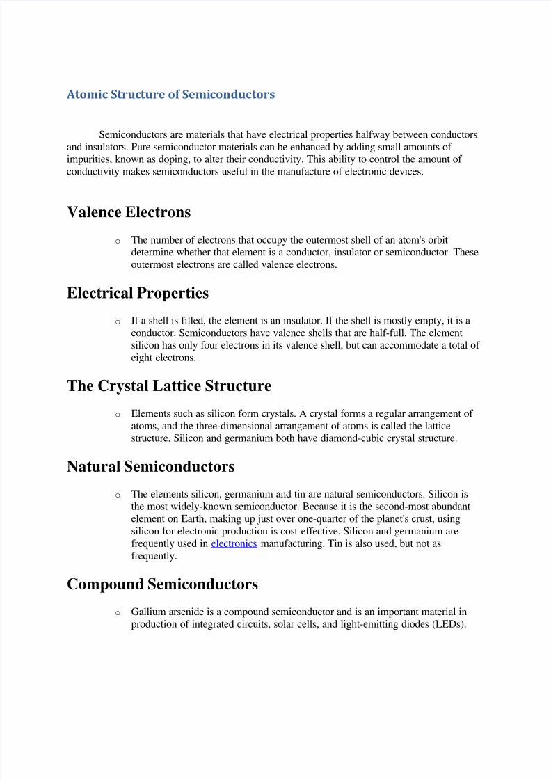
Basic Semiconductor Crystal Structure
To understand how diodes, transistors, and other semiconductor devices can do what they do, itis first necessary to understand the basic structure of all semiconductor devices. Early
semiconductors were fabricated from the element Germanium, but Silicon is preferred in most
modern applications.
The crystal structure of pure silicon is of course 3-dimensional, but that is difficult to display or
to see, so the image to the left is often used to represent the crystal structure of silicon. For you
physics types, silicon (and germanium) falls in column IVa of the Periodic Table. This is thecarbon family of elements. The essential characteristic of these elements is that each atom has
four electrons to share with adjacent atoms in forming bonds.
While this is an oversimplified description, the nature of a bond between two silicon atoms is
such that each atom provides one electron to share with the other. The two electrons thus sharedare in fact shared equally between the two atoms. This type of sharing is known as a covalent
bond . Such a bond is very stable, and holds the two atoms together very tightly, so that itrequires a lot of energy to break this bond.
For those who are interested, the actual bonds in a 3-dimensional silicon crystal are arranged at
equal angles from each other. If you visualize a tetrahedron (a pyramid with three points on the

8/4/2019 Mat Sci Datas
http://slidepdf.com/reader/full/mat-sci-datas 3/11
ground and a fourth point sticking straight up) with the atom centered inside, the four bonds will
be directed towards the points of the tetrahedron.
Now we have our silicon crystal, but we still don't have a semiconductor. In the crystal we saw
above, all of the outer electrons of all silicon atoms are used to make covalent bonds with other
atoms. There are no electrons available to move from place to place as an electrical current.Thus, a pure silicon crystal is quite a good insulator. In fact, it is almost glass, which is silicon
dioxide. A crystal of pure silicon is said to be an intrinsic crystal.
N-type
To allow our silicon crystal to conduct electricity, we must find a way to allow some electrons to
move from place to place within the crystal, in spite of the covalent bonds between atoms. One
way to accomplish this is to introduce an impurity such as Arsenic or Phosphorus into the crystalstructure, as shown to the right. These elements are from column Va of the Periodic Table, and
have five outer electrons to share with other atoms. In this application, four of these five
electrons bond with adjacent silicon atoms as before, but the fifth electron cannot form a bond.
This electron can easily be moved with only a small applied electrical voltage. Because theresulting crystal has an excess of current-carrying electrons, each with a negative charge, it is
known as "N-type" silicon.
This construction does not conduct electricity as easily and readily as, say, copper or silver. It
does exhibit some resistance to the flow of electricity. It cannot properly be called a conductor,
but at the same time it is no longer an insulator. Therefore, it is known as a semiconductor .
While this effect is interesting, it still isn't particularly useful by itself. A plain carbon resistor is
easier and cheaper to manufacture than a silicon semiconductor one. We still don't have any way
to actually control an electrical current.
p-type

8/4/2019 Mat Sci Datas
http://slidepdf.com/reader/full/mat-sci-datas 4/11
But wait a moment! We obtained a semiconductor material by introducing a 5-electron impurityinto a matrix of 4-electron atoms. (For you physics types, we're only looking at the outer
electrons that are available for bonding -- electrons in inner shells are not included in the process
or in this discussion.) What happens if we go the other way, and introduce a 3-electron impurity
into such a crystal? Suppose we introduce some Aluminum (from column IIIa in the PeriodicTable) into the crystal, as shown to the left? We could also try Gallium, which is also in column
IIIa right under aluminum. Now what?
These elements only have three electrons available to share with other atoms. Those three
electrons do indeed form covalent bonds with adjacent silicon atoms, but the expected fourth
bond cannot be formed. A complete connection is impossible here, leaving a "hole" in thestructure of the crystal.
Experimentation shows that there is an empty place where an electron should logically go, andoften an electron will try to move into that space to fill it. However, the electron filling the hole
had to leave a covalent bond behind to fill this empty space, and therefore leaves another hole
behind as it moves. Yet another electron may move into that hole, leaving another hole behind,
and so forth. In this manner, holes appear to move as positive charges through the crystal.
Therefore, this type of semiconductor material is designated "P-type" silicon.
http://www.play-hookey.com/semiconductors/basic_structure.html
ANIMATED intrinsic and extrinsic
http://www.tutorvista.com/content/physics/physics-iv/semiconductor-devices/intrinsic-and-extrinsic-
semiconductors.php
In the solid state physics field of semiconductors and insulators, the conduction band is therange of electron energies, higher than that of the valence band, sufficient to free an electron
from binding with its individual atom and allow it to move freely within the atomic lattice of thematerial. Electrons within the conduction band are mobile charge carriers in solids, responsible
for conduction of electric currents in metals and other good electrical conductors.

8/4/2019 Mat Sci Datas
http://slidepdf.com/reader/full/mat-sci-datas 5/11
Semiconductor band structure
http://en.wikipedia.org/wiki/Conduction_band
Semiconductor Materials
Whereas polymers are highly visible engineering materials with a major impact on contemporarysociety, semiconductors are relatively invisible but have a comparable social impact. Technology
has clearly revolutionized society, but solid-state electronics is revolutionizing technology itself.A relatively small group of elements and compounds has an important electrical property, semi-
conduction , in which they are neither good electrical conductors nor good electrical insulators.
Instead, their ability to conduct electricity is intermediate. These materials are called
semiconductors, and in general, they do not fit into any of the four structural materials
categories based on atomic bonding. Metals are inherently good electrical conductors. Ceramics
and polymers (non-metals) are generally poor conductors but good insulators. The three
semiconducting elements (Si, Ge, and Sn) from column IVA of the periodic table serve as a kindof boundary between metallic and nonmetallic elements. Silicon (Si) and germanium (Ge),
widely used elemental semiconductors, are excellent examples of this class of materials.[Another important semiconductor material is GaAs, a compound of the group IIIA element Ga;
and the group V element, As.]
Taken from Introduction to Materials Science for Engineers, James F. Shackelford, Pearson, Higher Education.
8/4/2019 Mat Sci Datas
http://slidepdf.com/reader/full/mat-sci-datas 6/11
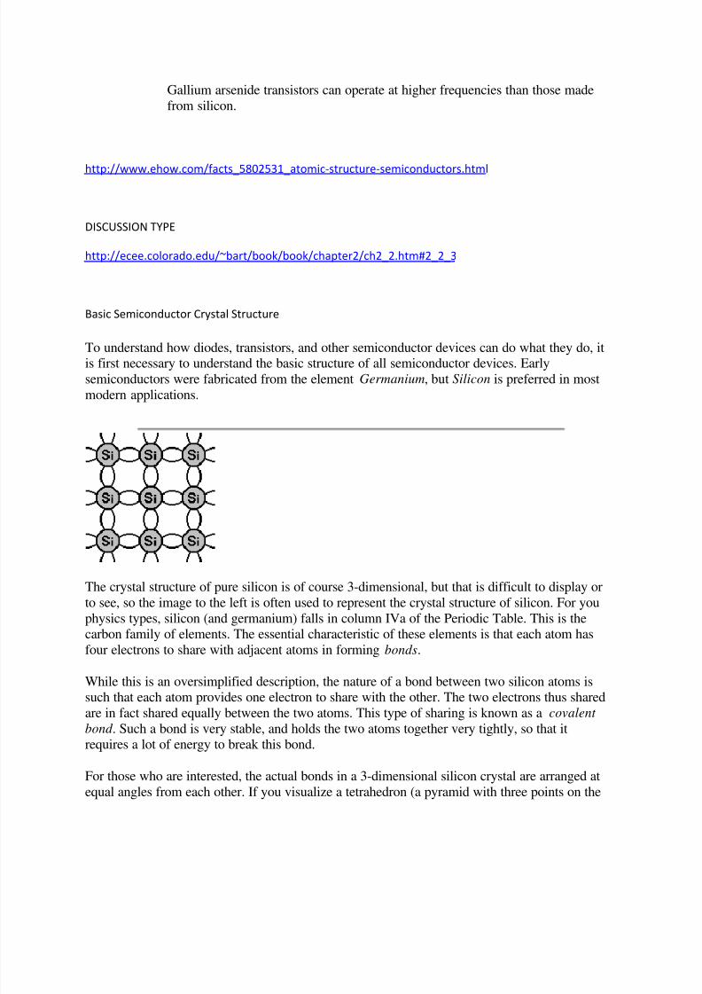
One area of materials engineering is
called "process engineering". It is
perhaps best illustrated by the
production of integrated circuitdevices. An excellent montage
representing IC processing is
illustrated in the following IBM gif.Behind the Process Engineer, one
see's a blow-up of the three-
dimensional array of metallizationlines that interconnect the various
device regions on an integrated
circuit. The gray substrate under the
pink, white, yellow and green metallization pattern, is the silicon wafer, which is a
semiconductor material. These interconnects are typically less than a micro-meter in thickness!The reference source URL is IBM chip technology
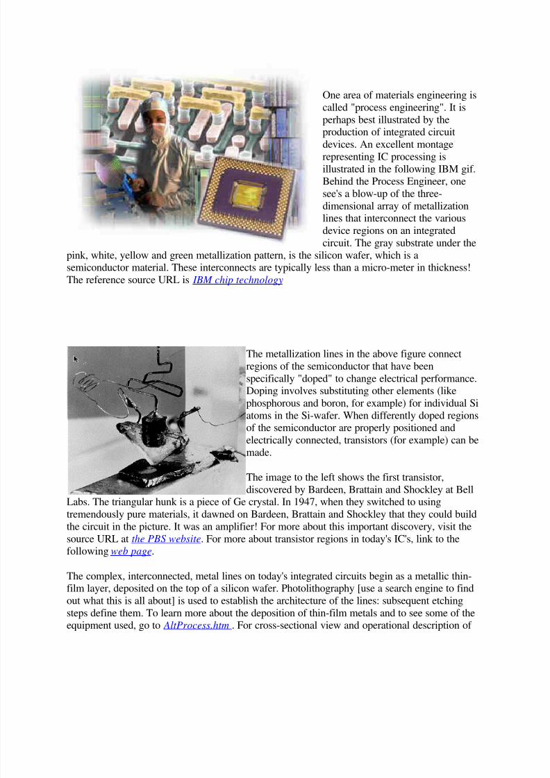
The metallization lines in the above figure connect
regions of the semiconductor that have been
specifically "doped" to change electrical performance.Doping involves substituting other elements (like
phosphorous and boron, for example) for individual Si
atoms in the Si-wafer. When differently doped regionsof the semiconductor are properly positioned and
electrically connected, transistors (for example) can be
made.
The image to the left shows the first transistor,
discovered by Bardeen, Brattain and Shockley at BellLabs. The triangular hunk is a piece of Ge crystal. In 1947, when they switched to using
tremendously pure materials, it dawned on Bardeen, Brattain and Shockley that they could build
the circuit in the picture. It was an amplifier! For more about this important discovery, visit the
source URL at the PBS website. For more about transistor regions in today's IC's, link to thefollowing web page.
The complex, interconnected, metal lines on today's integrated circuits begin as a metallic thin-film layer, deposited on the top of a silicon wafer. Photolithography [use a search engine to find
out what this is all about] is used to establish the architecture of the lines: subsequent etching
steps define them. To learn more about the deposition of thin-film metals and to see some of theequipment used, go to AltProcess.htm . For cross-sectional view and operational description of

8/4/2019 Mat Sci Datas
http://slidepdf.com/reader/full/mat-sci-datas 7/11
six different IC (Integrated Circuits) devices, visit these International Rectifier web pages. To see
detail of IC architecture, visit the Materials Characterization web pages of the WofMatE. The
pbs transistor web pages offer further detail of typical IC device concepts and architecture.
The products of the process engineer in the microelectronics industry are represented in this
montage (left), also from IBM . A typical IC (full die shot of the HP PA-8000 microprocessorusing oblique illumination with blue and red gels) is shown on the right. For more
photomicrographs of IC dies, visit these Florida State University web pages.
One step in the production of semiconductor devices involves the growth of a large (10 or more
inches in diameter!) single crystal of silicon by the Czochralski process. In this process, a solidseed crystal is rotated and slowly extracted from a pool of molten Si. This is shown above. The
various steps in the production of semiconductor devices are clearly illustrated on the web pages
of Fullman-Kinetics, the source of the Czochralski image-sequence, above. This is only an
example of he Fullman-Kinetics series "The Semiconductor Manufacturing Process". [The
Fullman-Kinetics web pages appear to no longer be available on the Internet, and this is a shame.They were excellent!] However, please visit the chip fabrication processing pages at this German
website. You may also wish to visit this San Jose State University link which outlines the basicstep of photolithography, an integral part of integrated circuit production.
In another IC processing step, after wafers of silicon are sliced from the single crystal and thenpolished, they are thermal-annealed in an oven. Below (left) we see Si wafers entering an oven
for an annealing treatment. This is taken from the Intel web pages.

8/4/2019 Mat Sci Datas
http://slidepdf.com/reader/full/mat-sci-datas 8/11
In a vacuum chamber, fine, intricate patterns are etched into silicon wafers with an ion discharge(above, right). This is another critical step in the production of integrated circuits. The violet
glow is emitted by the ion plasma. The plasma etching process makes possible the smallgeometries need for very large scale integration in silicon chips. This image is taken from the
Lucent Technologies web pages.
A really neat overview of the layer-by-layer creation of a solid state mircro-electronic device is
included on the FSU Molecular Expressions web pages at the following URL . You are highlyencouraged to visit and explore the Molecular Expressions web site!
The above images illustrate methods applicable to the fabrication of integrated circuits (IC's)[also termed "chips"] used in the production of microelectronic devices. The process engineer
plays a key role in the production of IC's. But the process engineer too is involved in the
packaging of these microelectronic devices; and in the assembly of packaged device on to theprinted circuit board (PCB). The whole sequence is quite elaborate and a comprehensive
treatment is well outside the scope of these web pages. However, I would like to introduce you to
one facet of IC packaging and that is the bonding of the IC chip to a suitable substrate. For this
example, consider "flip chip" technology. The respective images presented below have beenextracted from the flip chip, MEMS web pages of the MEMS Technology Application Center
which no longer exists. A brief overview of flip-chip packaging is presented in the following ,
now Maxtek link. Maxtek is a full-service custom microelectronics packaging provider.
'Flip chip' is a general term that describes a method of attaching an integrated circuit (ie, IC) to a
substrate. The substrate can be another chip, a PC board, a special carrier or a multichip module.
More specifically, flip chip is a technology in which one chip is placed face down (flip chipped)on to the substrate and attached through solder bumps that provide both mechanical and
electrical connection. Flip chip provides a much higher interconnection density than traditional
methods (i.e. wire bonding) because the interconnections are distributed across the entire chipsurface rather than being restricted to the periphery of the chip.
8/4/2019 Mat Sci Datas
http://slidepdf.com/reader/full/mat-sci-datas 9/11
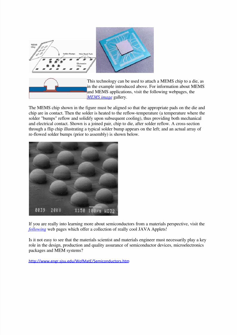
This technology can be used to attach a MEMS chip to a die, as
in the example introduced above. For information about MEMS
and MEMS applications, visit the following webpages, the
MEMS image gallery.
The MEMS chip shown in the figure must be aligned so that the appropriate pads on the die and
chip are in contact. Then the solder is heated to the reflow-temperature (a temperature where the
solder "bumps" reflow and solidify upon subsequent cooling), thus providing both mechanicaland electrical contact. Shown is a joined pair, chip to die, after solder reflow. A cross-section
through a flip chip illustrating a typical solder bump appears on the left; and an actual array of
re-flowed solder bumps (prior to assembly) is shown below.
If you are really into learning more about semiconductors from a materials perspective, visit the
following web pages which offer a collection of really cool JAVA Applets!
Is it not easy to see that the materials scientist and materials engineer must necessarily play a key
role in the design, production and quality assurance of semiconductor devices, microelectronicspackages and MEM systems?
http://www.engr.sjsu.edu/WofMatE/Semiconductors.htm
8/4/2019 Mat Sci Datas
http://slidepdf.com/reader/full/mat-sci-datas 10/11
Doping (semiconductor)
n semiconductor production, doping intentionally introduces impurities into an extremely pure
(also referred to as intrinsic) semiconductor for the purpose of modulating its electrical
properties. The impurities are dependent upon the type of semiconductor. Lightly and moderately
doped semiconductors are referred to as extrinsic. A semiconductor doped to such high levelsthat it acts more like a conductor than a semiconductor is referred to as degenerate.
In the context of phosphors and scintillators, doping is better known as activation.
History
Its effects were long known empirically in such devices as crystal radio detectors and selenium rectifiers.
However, semiconductor doping was formally first developed by John Robert Woodyard working at
Sperry Gyroscope Company during World War II.[1] The demands of his work on radar denied Woodyard
the opportunity to pursue research on semiconductor doping. However, after the war ended, his patent proved the grounds of extensive litigation by Sperry Rand.
[2] Related work was performed at Bell Labs by
Gordon K. Teal and Morgan Sparks.[3]
Process
Some dopants are added as the (usually silicon) boule is grown, giving each wafer an almost
uniform initial doping.[4]
To define circuit elements, selected areas — typically controlled by
photolithography[5] — are further doped by such processes as diffusion
[6] and ion implantation, the
latter method being more popular in large production runs because of increased controllability.
Small numbers of dopant atoms can change the ability of a semiconductor to conduct electricity.
When on the order of one dopant atom is added per 100 million atoms, the doping is said to be
low or light . When many more dopant atoms are added, on the order of one per ten thousandatoms, the doping is referred to as heavy or high. This is often shown as n+ for n-type doping or
p+ for p-type doping. (See the article on semiconductors for a more detailed description of the
doping mechanism.)
Dopant elements
(Note: When discussing periodic table groups, semiconductor physicists always use an older
notation, not the current IUPAC group notation. For example, the carbon group is called "GroupIV", not "Group 14".)
For the Group IV semiconductors such as silicon, germanium, and silicon carbide, the most
common dopants are acceptors from Group III or donors from Group V elements. Boron,
arsenic, phosphorus, and occasionally gallium are used to dope silicon. Boron is the p-type
dopant of choice for silicon integrated circuit production because it diffuses at a rate that makes junction depths easily controllable. Phosphorus is typically used for bulk-doping of silicon

8/4/2019 Mat Sci Datas
http://slidepdf.com/reader/full/mat-sci-datas 11/11
wafers, while arsenic is used to diffuse junctions, because it diffuses more slowly than
phosphorus and is thus more controllable.
By doping pure silicon with Group V elements such as phosphorus, extra valence electrons are
added that become unbonded from individual atoms and allow the compound to be an
electrically conductive n-type semiconductor. Doping with Group III elements, which aremissing the fourth valence electron, creates "broken bonds" (holes) in the silicon lattice that are
free to move. The result is an electrically conductive p-type semiconductor. In this context, aGroup V element is said to behave as an electron donor, and a group III element as an acceptor.
This is a key concept in the physics of a diode.
Very heavily doped semiconductor behaves more like a good conductor (metal) and thus exhibits
more linear positive thermal coefficient. Such effect is used for instance in sensistors.[7]
Lower
dosage of doping is used in other types (NTC or PTC) thermistors.
Compensation
In most cases many types of impurities will be present in the resultant doped semiconductor. If an equal number of donors and acceptors are present in the semiconductor, the extra core
electrons provided by the former will be used to satisfy the broken bonds due to the latter, so that
doping produces no free carriers of either type. This phenomenon is known as compensation, andoccurs at the p-n junction in the vast majority of semiconductor devices. Partial compensation,
where donors outnumber acceptors or vice versa, allows device makers to repeatedly reverse the
type of a given portion of the material by applying successively higher doses of dopants.
Although compensation can be used to increase or decrease the number of donors or acceptors,
the electron and hole mobility is always decreased by compensation because mobility is affected
by the sum of the donor and acceptor ions.
http://en.wikipedia.org/wiki/Doping_%28semiconductor%29