master's thesis · 2011-06-05 · master's thesis 액정 디스플레이를 이용한...
TRANSCRIPT
석 사 학 위 논 문석 사 학 위 논 문석 사 학 위 논 문석 사 학 위 논 문
Master's Thesis
액정액정액정액정 디스플레이를디스플레이를디스플레이를디스플레이를 이용한이용한이용한이용한 미세입자미세입자미세입자미세입자 및및및및
혈액세포의혈액세포의혈액세포의혈액세포의 광전자적광전자적광전자적광전자적 구동구동구동구동에에에에 관한관한관한관한 연구연구연구연구
Optoelectronic manipulation of microparticles and blood cells using
a liquid crystal display
황황황황 현현현현 두두두두 ( ( ( (黃黃黃黃 炫炫炫炫 斗斗斗斗 Hyundoo Hwang))))
바이오및뇌공학바이오및뇌공학바이오및뇌공학바이오및뇌공학과과과과 Department of Bio and Brain Engineering
한 국 과 학 기 술 원한 국 과 학 기 술 원한 국 과 학 기 술 원한 국 과 학 기 술 원
Korea Advanced Institute of Science and Technology
2007
액정액정액정액정 디스플레이를디스플레이를디스플레이를디스플레이를 이용한이용한이용한이용한 미세입자미세입자미세입자미세입자 및및및및
혈액세포의혈액세포의혈액세포의혈액세포의 광전자적광전자적광전자적광전자적 구동구동구동구동에에에에 관한관한관한관한 연구연구연구연구
Optoelectronic manipulation of
microparticles and blood cells using a
liquid crystal display
Optoelectronic manipulation of
microparticles and blood cells using a
liquid crystal display
Advisor: Professor Je-Kyun Park
by Hyundoo Hwang
Department of Bio and Brain Engineering
Korea Advanced Institute of Science and Technology
A thesis submitted to the faculty of the Korea Advanced Institute
of Science and Technology in partial fulfillment of the requirements
for the degree of Master of Science in the Department of Bio and
Brain Engineering
Daejeon, Korea
2007. 6. 26.
Approved by
Professor Je-Kyun Park

액정액정액정액정 디스플레이를디스플레이를디스플레이를디스플레이를 이용한이용한이용한이용한 미세입자미세입자미세입자미세입자 및및및및
혈액세포의혈액세포의혈액세포의혈액세포의 광전자적광전자적광전자적광전자적 구동에구동에구동에구동에 관한관한관한관한 연구연구연구연구
황황황황 현현현현 두두두두
위위위위 논문은논문은논문은논문은 한국과학기술원한국과학기술원한국과학기술원한국과학기술원 석사석사석사석사 학위논문으로학위논문으로학위논문으로학위논문으로 학위논문학위논문학위논문학위논문
심사위원회에서심사위원회에서심사위원회에서심사위원회에서 심사심사심사심사 통과하였음통과하였음통과하였음통과하였음....
2002002002007777 년년년년 6666 월월월월 22226666 일일일일
심사위원장심사위원장심사위원장심사위원장 박박박박 제제제제 균균균균 ((((인인인인))))
심사심사심사심사 위원위원위원위원 남남남남 윤윤윤윤 기기기기 ((((인인인인))))
심사심사심사심사 위원위원위원위원 정정정정 기기기기 훈훈훈훈 ((((인인인인))))
i
MBiS 20063643
황 현 두. Hyundoo Hwang. Optoelectronic Manipulation of Microparticles and Blood Cells using a Liquid Crystal Display. 액정 디스플레이를
이용한 미세입자 및 혈액세포의 광전자적 구동에 관한 연구. Department of Bio and Brain Engineering. 2007. 90p. Advisor Prof. Je-Kyun Park. Text in English.
Abstract
This thesis presents two types of approaches for enhancement of a typical optoelectronic
tweezers (OET). OET has been a powerful tool for cellular-scale manipulation of
microparticles in medical and biological applications. However, in a typical OET, non-specific
interactions between particles and device surfaces interfere with the effective particle
manipulation. Under applied electric fields, some attached particles induce strong dipole forces
and pull other particles around them. In order to overcome these problems, we suggest a novel
platform called three dimensional optoelectronic tweezers (3D OET) composed of double
photoconductive layers to focus microparticles vertically, providing adsorption-free
microparticle manipulation. The 3D OET was successfully applied to focus and manipulate
polystyrene microbeads in a channel-less microenvironment without adsorptions. It showed
higher particle trapping efficiency and stability than a typical OET.
There are three types of OET platforms; digital micro-mirror display (DMD) OET, image
DEP and lab-on-a-display. DMD OET and image DEP, which uses a DMD and a projector for
image generation respectively, require complex optical structures constructed with lens and
mirror for reflecting and focusing the light. In the case of a lab-on-a-display, it has the simplest
structure for portable application because it uses a direct light transfer of LCD without any
optical components. However, the lab-on-a-display has lower performances than others. To
overcome the limitations and to harmonize the advantages of each platform, we report a LCD-
based OET system integrated with a condenser lens and an interactive control system. The
LCD OET provides much higher performances than lab-on-a-display and simpler structures
than DMD OET and image DEP. The well-integrated system is successfully utilized for
interactive manipulation of red and white blood cells. This new LCD-based OET system using
a condenser lens and an LCD may be a usable integrated system for optoelectronic
manipulation of microparticles in many biological applications.
ii
Contents Abstract ⋅⋅⋅⋅⋅⋅⋅⋅⋅⋅⋅⋅⋅⋅⋅⋅⋅⋅⋅⋅⋅⋅⋅⋅⋅⋅⋅⋅⋅⋅⋅⋅⋅⋅⋅⋅⋅⋅⋅⋅⋅⋅⋅⋅⋅⋅⋅⋅⋅⋅⋅⋅⋅⋅⋅⋅⋅⋅⋅⋅⋅⋅⋅⋅⋅⋅⋅⋅⋅⋅⋅⋅⋅⋅⋅⋅⋅⋅⋅⋅⋅⋅⋅⋅⋅⋅⋅⋅⋅⋅⋅⋅⋅⋅⋅⋅⋅⋅⋅⋅⋅⋅⋅⋅⋅⋅⋅⋅⋅ i
Nomenclature ⋅⋅⋅⋅⋅⋅⋅⋅⋅⋅⋅⋅⋅⋅⋅⋅⋅⋅⋅⋅⋅⋅⋅⋅⋅⋅⋅⋅⋅⋅⋅⋅⋅⋅⋅⋅⋅⋅⋅⋅⋅⋅⋅⋅⋅⋅⋅⋅⋅⋅⋅⋅⋅⋅⋅⋅⋅⋅⋅⋅⋅⋅⋅⋅⋅⋅⋅⋅⋅⋅⋅⋅⋅⋅⋅⋅⋅⋅⋅⋅⋅⋅⋅⋅⋅⋅⋅⋅⋅⋅⋅⋅⋅⋅⋅⋅⋅⋅ iv
List of Tables ⋅⋅⋅⋅⋅⋅⋅⋅⋅⋅⋅⋅⋅⋅⋅⋅⋅⋅⋅⋅⋅⋅⋅⋅⋅⋅⋅⋅⋅⋅⋅⋅⋅⋅⋅⋅⋅⋅⋅⋅⋅⋅⋅⋅⋅⋅⋅⋅⋅⋅⋅⋅⋅⋅⋅⋅⋅⋅⋅⋅⋅⋅⋅⋅⋅⋅⋅⋅⋅⋅⋅⋅⋅⋅⋅⋅⋅⋅⋅⋅⋅⋅⋅⋅⋅⋅⋅⋅⋅⋅⋅⋅⋅⋅⋅⋅⋅⋅ vii
List of Figures ⋅⋅⋅⋅⋅⋅⋅⋅⋅⋅⋅⋅⋅⋅⋅⋅⋅⋅⋅⋅⋅⋅⋅⋅⋅⋅⋅⋅⋅⋅⋅⋅⋅⋅⋅⋅⋅⋅⋅⋅⋅⋅⋅⋅⋅⋅⋅⋅⋅⋅⋅⋅⋅⋅⋅⋅⋅⋅⋅⋅⋅⋅⋅⋅⋅⋅⋅⋅⋅⋅⋅⋅⋅⋅⋅⋅⋅⋅⋅⋅⋅⋅⋅⋅⋅⋅⋅⋅⋅⋅⋅⋅⋅⋅⋅ viii
Chapter 1. Introduction ⋅⋅⋅⋅⋅⋅⋅⋅⋅⋅⋅⋅⋅⋅⋅⋅⋅⋅⋅⋅⋅⋅⋅⋅⋅⋅⋅⋅⋅⋅⋅⋅⋅⋅⋅⋅⋅⋅⋅⋅⋅⋅⋅⋅⋅⋅⋅⋅⋅⋅⋅⋅⋅⋅⋅⋅⋅⋅⋅⋅⋅⋅⋅⋅⋅⋅⋅⋅⋅⋅⋅⋅⋅⋅⋅⋅⋅⋅⋅⋅⋅⋅ 1
1.1. Tools for microparticle manipulation ⋅⋅⋅⋅⋅⋅⋅⋅⋅⋅⋅⋅⋅⋅⋅⋅⋅⋅⋅⋅⋅⋅⋅⋅⋅⋅⋅⋅⋅⋅⋅⋅⋅⋅⋅⋅⋅⋅⋅⋅⋅⋅⋅⋅⋅⋅⋅⋅⋅⋅⋅⋅⋅⋅⋅⋅⋅⋅⋅⋅⋅⋅⋅⋅⋅⋅⋅ 1
1.2. Dielectrophoresis ⋅⋅⋅⋅⋅⋅⋅⋅⋅⋅⋅⋅⋅⋅⋅⋅⋅⋅⋅⋅⋅⋅⋅⋅⋅⋅⋅⋅⋅⋅⋅⋅⋅⋅⋅⋅⋅⋅⋅⋅⋅⋅⋅⋅⋅⋅⋅⋅⋅⋅⋅⋅⋅⋅⋅⋅⋅⋅⋅⋅⋅⋅⋅⋅⋅⋅⋅⋅⋅⋅⋅⋅⋅⋅⋅⋅⋅⋅⋅⋅⋅⋅⋅⋅⋅⋅⋅⋅⋅⋅⋅⋅⋅⋅⋅⋅⋅ 5
1.3. Optoelectronic tweezers ⋅⋅⋅⋅⋅⋅⋅⋅⋅⋅⋅⋅⋅⋅⋅⋅⋅⋅⋅⋅⋅⋅⋅⋅⋅⋅⋅⋅⋅⋅⋅⋅⋅⋅⋅⋅⋅⋅⋅⋅⋅⋅⋅⋅⋅⋅⋅⋅⋅⋅⋅⋅⋅⋅⋅⋅⋅⋅⋅⋅⋅⋅⋅⋅⋅⋅⋅⋅⋅⋅⋅⋅⋅⋅⋅⋅⋅⋅⋅⋅⋅⋅⋅⋅⋅⋅⋅ 8
1.4. Research objectives ⋅⋅⋅⋅⋅⋅⋅⋅⋅⋅⋅⋅⋅⋅⋅⋅⋅⋅⋅⋅⋅⋅⋅⋅⋅⋅⋅⋅⋅⋅⋅⋅⋅⋅⋅⋅⋅⋅⋅⋅⋅⋅⋅⋅⋅⋅⋅⋅⋅⋅⋅⋅⋅⋅⋅⋅⋅⋅⋅⋅⋅⋅⋅⋅⋅⋅⋅⋅⋅⋅⋅⋅⋅⋅⋅⋅⋅⋅⋅⋅⋅⋅⋅⋅⋅⋅⋅⋅⋅⋅⋅⋅ 13
1.5. Thesis outline ⋅⋅⋅⋅⋅⋅⋅⋅⋅⋅⋅⋅⋅⋅⋅⋅⋅⋅⋅⋅⋅⋅⋅⋅⋅⋅⋅⋅⋅⋅⋅⋅⋅⋅⋅⋅⋅⋅⋅⋅⋅⋅⋅⋅⋅⋅⋅⋅⋅⋅⋅⋅⋅⋅⋅⋅⋅⋅⋅⋅⋅⋅⋅⋅⋅⋅⋅⋅⋅⋅⋅⋅⋅⋅⋅⋅⋅⋅⋅⋅⋅⋅⋅⋅⋅⋅⋅⋅⋅⋅⋅⋅⋅⋅⋅⋅⋅⋅⋅⋅⋅ 14
Chapter 2. Three-Dimensional Optoelectronic Tweezers ⋅⋅⋅⋅⋅⋅⋅⋅⋅⋅⋅⋅⋅⋅⋅⋅⋅⋅⋅⋅⋅⋅⋅⋅⋅⋅ 15
2.1. Introduction ⋅⋅⋅⋅⋅⋅⋅⋅⋅⋅⋅⋅⋅⋅⋅⋅⋅⋅⋅⋅⋅⋅⋅⋅⋅⋅⋅⋅⋅⋅⋅⋅⋅⋅⋅⋅⋅⋅⋅⋅⋅⋅⋅⋅⋅⋅⋅⋅⋅⋅⋅⋅⋅⋅⋅⋅⋅⋅⋅⋅⋅⋅⋅⋅⋅⋅⋅⋅⋅⋅⋅⋅⋅⋅⋅⋅⋅⋅⋅⋅⋅⋅⋅⋅⋅⋅⋅⋅⋅⋅⋅⋅⋅⋅⋅⋅⋅⋅⋅⋅⋅⋅⋅⋅ 15
2.2. Design and fabrication ⋅⋅⋅⋅⋅⋅⋅⋅⋅⋅⋅⋅⋅⋅⋅⋅⋅⋅⋅⋅⋅⋅⋅⋅⋅⋅⋅⋅⋅⋅⋅⋅⋅⋅⋅⋅⋅⋅⋅⋅⋅⋅⋅⋅⋅⋅⋅⋅⋅⋅⋅⋅⋅⋅⋅⋅⋅⋅⋅⋅⋅⋅⋅⋅⋅⋅⋅⋅⋅⋅⋅⋅⋅⋅⋅⋅⋅⋅⋅⋅⋅⋅⋅⋅⋅⋅⋅ 17
2.3. Simulation of electric field distribution ⋅⋅⋅⋅⋅⋅⋅⋅⋅⋅⋅⋅⋅⋅⋅⋅⋅⋅⋅⋅⋅⋅⋅⋅⋅⋅⋅⋅⋅⋅⋅⋅⋅⋅⋅⋅⋅⋅⋅⋅⋅⋅⋅⋅⋅⋅⋅⋅⋅⋅⋅⋅⋅⋅⋅⋅⋅⋅⋅⋅⋅ 22
2.4. Experimental ⋅⋅⋅⋅⋅⋅⋅⋅⋅⋅⋅⋅⋅⋅⋅⋅⋅⋅⋅⋅⋅⋅⋅⋅⋅⋅⋅⋅⋅⋅⋅⋅⋅⋅⋅⋅⋅⋅⋅⋅⋅⋅⋅⋅⋅⋅⋅⋅⋅⋅⋅⋅⋅⋅⋅⋅⋅⋅⋅⋅⋅⋅⋅⋅⋅⋅⋅⋅⋅⋅⋅⋅⋅⋅⋅⋅⋅⋅⋅⋅⋅⋅⋅⋅⋅⋅⋅⋅⋅⋅⋅⋅⋅⋅⋅⋅⋅⋅⋅⋅⋅⋅ 24
2.5. Results and discussion ⋅⋅⋅⋅⋅⋅⋅⋅⋅⋅⋅⋅⋅⋅⋅⋅⋅⋅⋅⋅⋅⋅⋅⋅⋅⋅⋅⋅⋅⋅⋅⋅⋅⋅⋅⋅⋅⋅⋅⋅⋅⋅⋅⋅⋅⋅⋅⋅⋅⋅⋅⋅⋅⋅⋅⋅⋅⋅⋅⋅⋅⋅⋅⋅⋅⋅⋅⋅⋅⋅⋅⋅⋅⋅⋅⋅⋅⋅⋅⋅⋅⋅⋅⋅⋅⋅⋅ 26
2.6. Conclusion ⋅⋅⋅⋅⋅⋅⋅⋅⋅⋅⋅⋅⋅⋅⋅⋅⋅⋅⋅⋅⋅⋅⋅⋅⋅⋅⋅⋅⋅⋅⋅⋅⋅⋅⋅⋅⋅⋅⋅⋅⋅⋅⋅⋅⋅⋅⋅⋅⋅⋅⋅⋅⋅⋅⋅⋅⋅⋅⋅⋅⋅⋅⋅⋅⋅⋅⋅⋅⋅⋅⋅⋅⋅⋅⋅⋅⋅⋅⋅⋅⋅⋅⋅⋅⋅⋅⋅⋅⋅⋅⋅⋅⋅⋅⋅⋅⋅⋅⋅⋅⋅⋅⋅⋅⋅ 34
Chapter 3. Lens-integrated LCD-based Optoelectronic Tweezers ⋅⋅⋅⋅⋅⋅⋅⋅⋅⋅⋅ 35
3.1. Introduction ⋅⋅⋅⋅⋅⋅⋅⋅⋅⋅⋅⋅⋅⋅⋅⋅⋅⋅⋅⋅⋅⋅⋅⋅⋅⋅⋅⋅⋅⋅⋅⋅⋅⋅⋅⋅⋅⋅⋅⋅⋅⋅⋅⋅⋅⋅⋅⋅⋅⋅⋅⋅⋅⋅⋅⋅⋅⋅⋅⋅⋅⋅⋅⋅⋅⋅⋅⋅⋅⋅⋅⋅⋅⋅⋅⋅⋅⋅⋅⋅⋅⋅⋅⋅⋅⋅⋅⋅⋅⋅⋅⋅⋅⋅⋅⋅⋅⋅⋅⋅⋅⋅⋅⋅ 35
3.2. Design and fabrication ⋅⋅⋅⋅⋅⋅⋅⋅⋅⋅⋅⋅⋅⋅⋅⋅⋅⋅⋅⋅⋅⋅⋅⋅⋅⋅⋅⋅⋅⋅⋅⋅⋅⋅⋅⋅⋅⋅⋅⋅⋅⋅⋅⋅⋅⋅⋅⋅⋅⋅⋅⋅⋅⋅⋅⋅⋅⋅⋅⋅⋅⋅⋅⋅⋅⋅⋅⋅⋅⋅⋅⋅⋅⋅⋅⋅⋅⋅⋅⋅⋅⋅⋅⋅⋅⋅⋅ 37
3.3. Simulation of electric field distribution ⋅⋅⋅⋅⋅⋅⋅⋅⋅⋅⋅⋅⋅⋅⋅⋅⋅⋅⋅⋅⋅⋅⋅⋅⋅⋅⋅⋅⋅⋅⋅⋅⋅⋅⋅⋅⋅⋅⋅⋅⋅⋅⋅⋅⋅⋅⋅⋅⋅⋅⋅⋅⋅⋅⋅⋅⋅⋅⋅⋅⋅ 40
3.4. Experimental ⋅⋅⋅⋅⋅⋅⋅⋅⋅⋅⋅⋅⋅⋅⋅⋅⋅⋅⋅⋅⋅⋅⋅⋅⋅⋅⋅⋅⋅⋅⋅⋅⋅⋅⋅⋅⋅⋅⋅⋅⋅⋅⋅⋅⋅⋅⋅⋅⋅⋅⋅⋅⋅⋅⋅⋅⋅⋅⋅⋅⋅⋅⋅⋅⋅⋅⋅⋅⋅⋅⋅⋅⋅⋅⋅⋅⋅⋅⋅⋅⋅⋅⋅⋅⋅⋅⋅⋅⋅⋅⋅⋅⋅⋅⋅⋅⋅⋅⋅⋅⋅⋅ 44
3.5. Results and discussion ⋅⋅⋅⋅⋅⋅⋅⋅⋅⋅⋅⋅⋅⋅⋅⋅⋅⋅⋅⋅⋅⋅⋅⋅⋅⋅⋅⋅⋅⋅⋅⋅⋅⋅⋅⋅⋅⋅⋅⋅⋅⋅⋅⋅⋅⋅⋅⋅⋅⋅⋅⋅⋅⋅⋅⋅⋅⋅⋅⋅⋅⋅⋅⋅⋅⋅⋅⋅⋅⋅⋅⋅⋅⋅⋅⋅⋅⋅⋅⋅⋅⋅⋅⋅⋅⋅⋅ 47
3.5.1. Simulation of Clausius-Mossotti factors⋅⋅⋅⋅⋅⋅⋅⋅⋅⋅⋅⋅⋅⋅⋅⋅⋅⋅⋅⋅⋅⋅⋅⋅⋅⋅⋅⋅⋅⋅⋅⋅⋅⋅⋅⋅⋅⋅⋅⋅⋅⋅ 47
iii
3.5.2. Condensation of LCD image ⋅⋅⋅⋅⋅⋅⋅⋅⋅⋅⋅⋅⋅⋅⋅⋅⋅⋅⋅⋅⋅⋅⋅⋅⋅⋅⋅⋅⋅⋅⋅⋅⋅⋅⋅⋅⋅⋅⋅⋅⋅⋅⋅⋅⋅⋅⋅⋅⋅⋅⋅⋅⋅⋅⋅⋅⋅⋅ 51
3.5.3. Polystyrene bead manipulation ⋅⋅⋅⋅⋅⋅⋅⋅⋅⋅⋅⋅⋅⋅⋅⋅⋅⋅⋅⋅⋅⋅⋅⋅⋅⋅⋅⋅⋅⋅⋅⋅⋅⋅⋅⋅⋅⋅⋅⋅⋅⋅⋅⋅⋅⋅⋅⋅⋅⋅⋅⋅⋅⋅⋅ 52
3.5.4. Blood cell manipulation ⋅⋅⋅⋅⋅⋅⋅⋅⋅⋅⋅⋅⋅⋅⋅⋅⋅⋅⋅⋅⋅⋅⋅⋅⋅⋅⋅⋅⋅⋅⋅⋅⋅⋅⋅⋅⋅⋅⋅⋅⋅⋅⋅⋅⋅⋅⋅⋅⋅⋅⋅⋅⋅⋅⋅⋅⋅⋅⋅⋅⋅⋅⋅⋅⋅⋅ 57
3.6. Conclusion ⋅⋅⋅⋅⋅⋅⋅⋅⋅⋅⋅⋅⋅⋅⋅⋅⋅⋅⋅⋅⋅⋅⋅⋅⋅⋅⋅⋅⋅⋅⋅⋅⋅⋅⋅⋅⋅⋅⋅⋅⋅⋅⋅⋅⋅⋅⋅⋅⋅⋅⋅⋅⋅⋅⋅⋅⋅⋅⋅⋅⋅⋅⋅⋅⋅⋅⋅⋅⋅⋅⋅⋅⋅⋅⋅⋅⋅⋅⋅⋅⋅⋅⋅⋅⋅⋅⋅⋅⋅⋅⋅⋅⋅⋅⋅⋅⋅⋅⋅⋅⋅⋅⋅⋅⋅ 62
Chapter 4. Conclusions ⋅⋅⋅⋅⋅⋅⋅⋅⋅⋅⋅⋅⋅⋅⋅⋅⋅⋅⋅⋅⋅⋅⋅⋅⋅⋅⋅⋅⋅⋅⋅⋅⋅⋅⋅⋅⋅⋅⋅⋅⋅⋅⋅⋅⋅⋅⋅⋅⋅⋅⋅⋅⋅⋅⋅⋅⋅⋅⋅⋅⋅⋅⋅⋅⋅⋅⋅⋅⋅⋅⋅⋅⋅⋅⋅⋅⋅⋅⋅⋅⋅ 63
Summary in Korean ⋅⋅⋅⋅⋅⋅⋅⋅⋅⋅⋅⋅⋅⋅⋅⋅⋅⋅⋅⋅⋅⋅⋅⋅⋅⋅⋅⋅⋅⋅⋅⋅⋅⋅⋅⋅⋅⋅⋅⋅⋅⋅⋅⋅⋅⋅⋅⋅⋅⋅⋅⋅⋅⋅⋅⋅⋅⋅⋅⋅⋅⋅⋅⋅⋅⋅⋅⋅⋅⋅⋅⋅⋅⋅⋅⋅⋅⋅⋅⋅⋅⋅⋅⋅⋅⋅ 69
References
Acknowledgements
Curriculum Vitae

iv
Nomenclature
Alphabetic letters
E Local electric field
fCM Clausius-Mossotti factor
Re(fCM) Real part of Clausius-Mossotti factor
FDEP Dielectrophoretic force
r Radius of a particle

v
Greek letters
δ Thickness of the cell membrane
εm Absolute permittivity of the suspending medium
εp Absolute permittivity of the particle
ε* Complex permittivity
εr Relative permittivity
σ Electrical conductivity
ω Natural frequency of AC voltage signal
vi
Abbreviations
CFD Computational Fluid Dynamics
CMOS Complementary Metal-Oxide Semiconductor
DEP Dielectrophoresis
DMD Digital Micro-mirror Device
iDEP Image Dielectrophoresis
ITO Indium Tin Oxide
LCD Liquid Crystal Display
MACS Magnetic-Activated Cell Sorter
N.A. Numerical Aperture
OET Optoelectronic Tweezers
PECVD Plasma Enhanced Chemical Vapor Deposition
PBS Phosphate Buffered Saline
PR Photoresist
TFT Thin Film Transistor
vii
List of Tables
Table 1. Different types of typical optoelectronic tweezers. ························12
viii
List of Figures
Figure 1. Dielectrophoretic movements of microparticles exposed to non-
uniform electric fields. ························································································7
Figure 2. Energy conversion process in optoelectronic tweezers. ····················10
Figure 3. Particle adsorptions in a typical OET device. ···································16
Figure 4. Schematic diagram of (a) optoelectronic tweezers (OET) and (b)
three-dimensional optoelectronic tweezers (3D OET).····································19
Figure 5. Fabrication process of OET device (left) and 3D OET device (right).
··························································································································21
Figure 6. Fabricated photoconductive layer.·····················································21
Figure 7. Simulated electric distributions in the liquid chamber of (a) OET and
(b) 3D OET. ······································································································23
Figure 8. Experimental setup for characterization of 3D OET. ························26
Figure 9. Microscopic photographs according to the heights of the liquid layer
of (a) OET and (b) 3D OET devices. ································································27

ix
Figure 10. Percentages of moving beads by several LCD images in OET and
3D OET devices (mean±standard deviation, n≥5).···········································29
Figure 11. Microscopic photographs of polystyrene beads (45 µm diameter)
concentrated by (a) OET and (b) 3D OET devices.··········································29
Figure 12. Percentages of moving beads according to their sizes in OET and
3D OET devices (mean±standard deviation, n≥5).···········································31
Figure 13. Bead velocities according to their sizes in OET and 3D OET devices.
(a) Bead velocities of moving beads (mean±standard deviation, n≥20). (b)
Average velocities of all beads including adsorbed beads.·······························32
Figure 14. Percentages of moving beads according to the time in OET and 3D
OET devices (mean±standard deviation, n≥5).·················································33
Figure 15. Microscopic photographs of (a) an original LCD image and (b) a
blurred image on a photoconductive layer. ·······················································36
Figure 16. Configuration of (a) a typical lab-on-a-display and (b) a new LCD-
based OET system integrated with a condenser lens. ·······································38
Figure 17. Fabrication process for the OET device. ·········································39
x
Figure 18. Microscopic photograph of the edge region of the blurred virtual
electrode and the measured light intensity of the image (thin line). The applied
voltages estimated based on the measured light intensity are described (thick
line) in the condition of 10 V bias.····································································41
Figure 19. Simulated distributions of electric field induced from (a) a clear
virtual electrode formed by condensed light and from (b) a blurred virtual
electrode formed by diffracted light in the condition of 10 V at 100 kHz.·······43
Figure 20. Plot of the square of electric field generated by a clear virtual
electrode (blue, solid) and a blurred virtual electrode (red, dotted) in the middle
of the liquid chamber. ·······················································································43
Figure 21. Schematic diagram of experimental setup for new LCD-based OET
system integrated with a condenser lens.··························································45
Figure 22. The simulated real part of Clausius-Mossotti factor of a 15 µm
diameter size polystyrene bead in mediums with conductivities of 1 S/m, 100
mS/m, 10 mS/m, 1 mS/m, and 0.1 mS/m. ························································48
Figure 23. The simulated real part of Clausius-Mossotti factor of a red blood
cell in mediums with conductivities of 1 S/m, 100 mS/m, 10 mS/m, 1 mS/m,
xi
and 0.1 mS/m. ···································································································50
Figure 24. Microscopic photographs of (a) an original LCD image and (b) a
condensed image on a photoconductive layer.··················································52
Figure 25. Bead velocities according to their sizes in a new LCD-based OET
system and a lab-on-a-display (mean±standard deviation, n≥20). ···················53
Figure 26. The captured photographs after parallel manipulation of 15 µm
polystyrene beads.·····························································································53
Figure 27. Bead velocities according to their sizes in 20 µm and 120 µm height
liquid chambers of OET device (mean±standard deviation, n≥20). ·················55
Figure 28. Interactive manipulation of a polystyrene bead for threading a maze
constructed by optically-induced virtual electrodes. ········································56
Figure 29. Concentration of red blood cells using a LCD image forming a word
“KAIST” during 60 seconds. (a) Voltage is not applied. (b) Voltage is applied.
··························································································································58
Figure 30. Parallel manipulation of red blood cells trapped in a virtual
electrodes array. ································································································58
xii
Figure 31. Single red blood cell manipulation.·················································59
Figure 32. Selection and manipulation of a single white blood cell among many
red blood cells in the condition of 7 V bias at 200 kHz.···································61

1
Chapter 1 Introduction
1.1. Tools for microparticle manipulation
The cellular-scale manipulation of microparticles plays important roles
in many fields of biological and medical applications[1, 2]. Functions such as
transporting, trapping and sorting of microscopic particles and cells are
essential to perform several biological and chemical applications including
bead-based chemical analysis, cell analysis, cell culture, and diagnostics in
clinical fields. For these purposes, several mechanisms such as optical[3],
magnetic[4], electrokinetic[5], acoustic[6] and hydrodynamic[7] forces have
been applied.
Optical tweezers which uses the optical force induced by the photon
momentum transferred from the incident light beam to the target particle was
first reported by Ashkin and his coworkers at AT&T Bell Laboratories in
1970[8, 9]. It has become a powerful tool for trapping cells and probing the
physical properties of biological polymers. A focused laser beam can generate
two forces; the scattering force which is proportional to the light intensity and
points in the direction of the incident light, and the gradient force which is
proportional to the gradient of intensity and points in the direction of the
2
intensity gradient. In practice, the gradient force needs to be more dominant
than the scattering force for stable particle trapping. For that condition, the
beam should diverge rapidly enough away from the focal point via a
microscope objective lens, whose high numerical aperture (N.A.) and well
corrected aberration focus light as tightly as possible[3]. Single cells, viruses
and bacteria were also trapped and manipulated by a tightly focused laser beam
with wavelength at the near infrared window without optical damages due to
the heat generated from adsorption of the strong incident laser beam[10, 11].
However, the small field of view of the high N.A. objective lens limits
the effective manipulation area less than 100 × 100 µm2. Because of the small
effective area for particle manipulation, the capability of parallel manipulation
is limited to a small number of cells. The manipulation area can be increased
by using a low N.A. objective lens, but the strength of the gradient force
decreases, resulting in a less stable particle trapping. A requirement of the high
light intensity for stable and multiple optical traps is also limitation of the
optical tweezers. The optical power required for multiple traps is proportional
to the number of traps[12, 13]. The maximum power of laser beam is limited
by the photo-damage threshold of light-sensitive components, limiting the
number of traps.
3
Magnetic forces are frequently used for the cell sorting, because
magnetic fields affect the target cells less than the other fields such as optical
and electrical field. Functionalized magnetic beads containing a large number
of superparamagnetic nanoparticles are used to attach to the target cells and
sort them out by applying a magnetic field in the magnetic-activated cell sorter
(MACS)[14-17]. For the single cell manipulation using a high resolution
magnetic field, microelectromagnetic matrix has been developed[18]. Recently,
a magnetic force microscope constructed with magnetic tip and trap platform
has been proposed for manipulation and sorting of single cells[4].
However, magnetic tweezers also has some limitations. We should
attach magnetic beads to the target cells for magnetic manipulation. The
magnetic bead attachment may affect the properties of the cells and interfere
with the observation. Although the magnetic force microscope and the
microelectromagnetic matrix may be used to manipulate single cells, the
requirement of a complex and expensive system and low density condition of
the cells makes them less attractive for the biological applications. In addition,
parallel manipulation of multiple cells using a magnetic field still remains
challenging.
Electrokinetic mechanisms are also widely used for microparticle
4
manipulation in a microfluidic device. There are three frequently used
electrokinetic mechanisms: electrophoresis[19, 20], dielectrophoresis[5, 21],
and electro-osmosis[5, 22]. Electrophoresis refers to the migration of an
electrically charged substance such as DNA and protein under the influence of
an electric field. In the electrophoresis, the target particles or molecules are
sorted by their own electrophoretic mobility under the same electric field
strength. Dielectrophoresis (DEP) is a phenomenon in which a force is exerted
on a dielectric particle when it is subjected to a non-uniform electric field. The
dielectrophoretic force does not require the particle to be charged differently
from the electrophoresis. It is proportional to the volume of the target particles
and the square of electric field gradient. Electo-osmosis is the motion of polar
liquid under the influence of an applied electric field. Since the electro-osmotic
drag force acting on nanoparticles is significantly larger than the
dielectrophoretic forces on them, the concentration of nanoparticles using the
electro-osmotic fluids is more effective than that using the dielectrophoresis.
These electrokinetic mechanisms are the most favorable tools for the
microparticle manipulation because any modification of target particle is not
needed and the construction of patterned electrode array for the parallel
manipulation with lower power consumption and larger manipulation area is
5
possible.
However, when we use an electrokinetic mechanism for manipulating
microparticles, relative permittivity and conductivity of the target particles and
the media need to be considered. The AC frequency-dependant properties of
AC electrokinetic manipulation techniques also limit the applicable ranges of
the electrokinetic mechanisms in biological applications.
1.2. Dielectrophoresis
Dielectrophoresis(DEP) is the movement of dielectric particles under a
non-uniform electric field driven by forces arising from the interaction between
the induced electric dipole of the particle and the applied electric field[23]. The
dielectrophoretic force is[24, 25]:
FDEP = 2πr3εmRe(fCM)∇E2
(1)
where is the radius of the particles, εm is the permittivity of media, E is the
local electric field, and Re(fCM) is the real part of the Clausius-Mossotti factor
which is described as below:
6
(2)
where ε* is the complex permittivity (ε* = ε-jσ/ω); σ is the conductivity, and ω
is the electric field frequency.
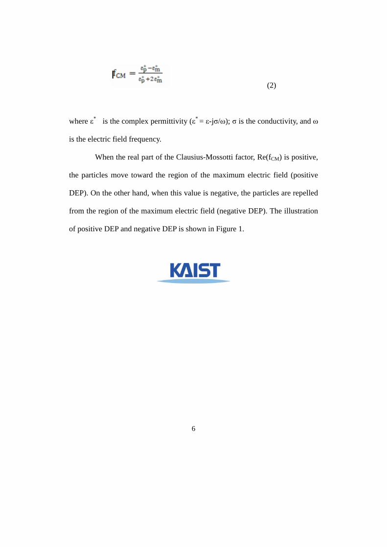
When the real part of the Clausius-Mossotti factor, Re(fCM) is positive,
the particles move toward the region of the maximum electric field (positive
DEP). On the other hand, when this value is negative, the particles are repelled
from the region of the maximum electric field (negative DEP). The illustration
of positive DEP and negative DEP is shown in Figure 1.
7
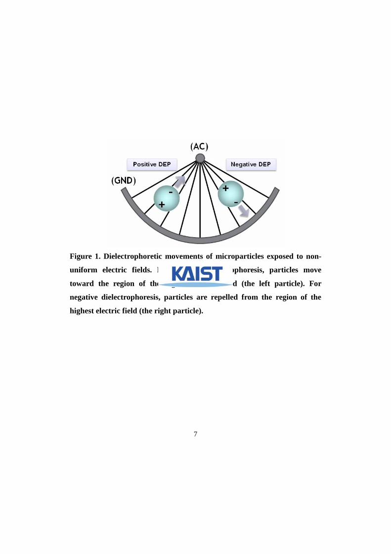
Figure 1. Dielectrophoretic movements of microparticles exposed to non-
uniform electric fields. For positive dielectrophoresis, particles move
toward the region of the highest electric field (the left particle). For
negative dielectrophoresis, particles are repelled from the region of the
highest electric field (the right particle).
8
1.3. Optoelectronic Tweezers
Electrokinetics, especially DEP, has become one of the most attractive
techniques for microparticle manipulation in a microfluidic device or a lab-on-
a-chip due to its ability to handle microparticles without any modification of
them. Many research groups have revealed the dielectric properties of
polystyrene microbeads[26-28], nanoparticles[29], carbon nanotubes[30, 31],
DNA[32, 33], bacteria[34], viruses[35], leukocytes[36], erythrocytes[37], liver
cells[38], and tumor cells[39].
Recently, a programmable lab-on-a-chip system using DEP electrode
array has been a key issue for parallel manipulation of individual cells or
particles[39, 40]. Manaresi and his colleagues reported a programmable DEP
technique which uses complementary metal-oxide semiconductor (CMOS)
circuit[41]. It was demonstrated that the programmable DEP manipulator with
individually addressable two-dimensional electrode array could be used for the
parallel manipulations of biological cells and microparticles. Since the
activated electrode patterns are movable and reconfigurable, it has many
advantages such as single particle addressing and selection, parallel
manipulation, and channel-less structure. However, it has a potential drawback
for disposable applications due to high manufacturing cost. Integration of on-
9
chip circuits increases the cost of the device, making it less attractive for
disposable applications. The wiring and interconnecting of the large number of
electrode array are also remained challenging issues.
To deal with these problems, optoelectronic tweezers (OET) was
proposed by Chiou and his colleagues in 2005[42]. In their study, replacing the
patterned electrodes with a pattern-less photoconductive layer, light-induced
virtual electrodes were formed on the photoconductive layer by using the
transmitted dynamic images generated from a digital micro-mirror device
(DMD). The conversion process among optical, electrical and mechanical
energy in OET is illustrated in Figure 2. In OET, the optical energy is
converted to the electrical energy via photoconductive material, triggering
virtual electrodes on the photoconductive surface. The virtual electrodes induce
the mechanical forces for microparticle manipulation via electrokinetic
mechanisms such as electrophoresis, dielectrophoresis, and electro-osmosis.
10
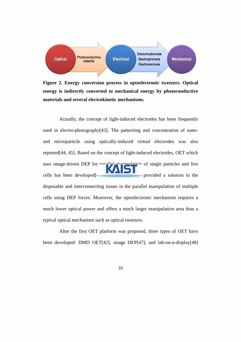
Figure 2. Energy conversion process in optoelectronic tweezers. Optical
energy is indirectly converted to mechanical energy by photoconductive
materials and several electrokinetic mechanisms.
Actually, the concept of light-induced electrodes has been frequently
used in electro-photography[43]. The patterning and concentration of nano-
and microparticle using optically-induced virtual electrodes was also
reported[44, 45]. Based on the concept of light-induced electrodes, OET which
uses image-driven DEP for parallel manipulation of single particles and live
cells has been developed[42, 46]. This concept provided a solution to the
disposable and interconnecting issues in the parallel manipulation of multiple
cells using DEP forces. Moreover, the optoelectronic mechanism requires a
much lower optical power and offers a much larger manipulation area than a
typical optical mechanism such as optical tweezers.
After the first OET platform was proposed, three types of OET have
been developed: DMD OET[42], image DEP[47], and lab-on-a-display[48]
11
(Table 1). The DMD OET is the first reported OET technique proposed by
Chiou and his colleagues as we mentioned. The DMD and optical lens
constructions offer the high resolution images to induce a virtual electrode.
However, the optical constructions for DMD projection lead to difficulties in
portable applications. The reflective structure resulted in complex structure.
Additionally, the optical lens between DMD and OET requires optical
alignment to focus the projected image on the photoconductive layer.
An OET system called image DEP (iDEP) uses a TFT-LCD projector
for image projection. This platform also needs a complex optical structure. In
addition, the images from the projector are diffracted more than DMD OET,
resulting in the lower-resolution virtual electrodes for particle manipulation.
The concept of an effective radius which is the maximum distance from a light
spot to manipulating particles is presented in their approach.
A lab-on-a-display, reported by Choi and his colleagues in 2007, is
constructed with an OET device and an LCD. The direct image transfer on
LCD is utilized. There is no optical component between LCD and OET, thus
the OET part is just placed on the display device. It offers the simplest structure
and the largest manipulation area among three types of OET platforms. In
addition, due to the elimination of lens and optical alignment, this platform is
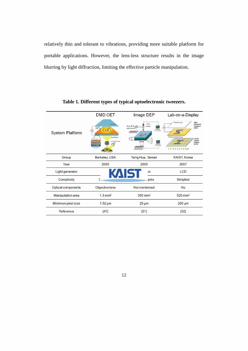
12
relatively thin and tolerant to vibrations, providing more suitable platform for
portable applications. However, the lens-less structure results in the image
blurring by light diffraction, limiting the effective particle manipulation.
Table 1. Different types of typical optoelectronic tweezers.
13
1.4. Research Objectives
In this paper, we have developed a new platform for optoelectronic
particle manipulation called three-dimensional optoelectronic tweezers (3D
OET) composed of two photoconductive layers. The 3D OET was successfully
applied to focus polystyrene beads vertically and to manipulate them without
adsorptions. This work demonstrates that vertical focusing of microbeads
prevents non-specific interactions between the particles and the surfaces of the
OET device, and provides increased trapping efficiency and adsorption-free
manipulation of the particles. The performance of 3D OET is also compared
with that of a typical OET.
Here, we also propose a new LCD-based OET platform integrated with
a condenser lens for condensing LCD images to prevent image blurring by
light diffraction. A simple experimental setup and high performances of new
LCD OET are demonstrated. Simulation studies for electric field distribution in
liquid chamber by blurred virtual electrodes in lab-on-a-display and clear
virtual electrodes in new LCD OET are also performed. The microbead
velocities according to their sizes and gap heights of liquid chamber in LCD-
condenser OET are measured and compared with those in a typical lab-on-a-
display. We also manipulated blood cells using this new LCD OET system.
14
1.5. Thesis outline
The thesis consists of four chapters. In Chapter 1, backgrounds and
research objectives are mentioned. Chapter 2 describes design, fabrication,
simulation, and experimental demonstration of 3D OET comparing with
conventional OET. Chapter 3 describes a new LCD-based OET system using a
condenser lens. The last chapter is the conclusions of this thesis.

15
Chapter 2 Three-Dimensional Optoelectronic Tweezers
2.1. Introduction
In a typical OET device, not only lateral forces but also vertical forces
act on the particles. The vertical forces make the particles move upward when a
negative DEP is induced. Consequently, the particles positioned at the upper
region of the liquid layer are frequently attached to the top ground layer by
surface-particle electrostatic interactions, interfering with the effective and
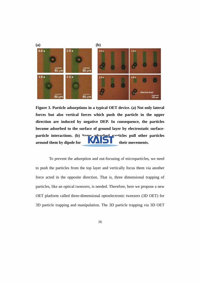
non-contact particle manipulation using OET. The attachment of microparticle
is shown in Figure 3(a). Some attached particles pull other nearby particles
around them by dipole forces and interfere with their smooth movements
(Figure 3(b)). Additionally, some relatively small particles are sometimes put
out of focus, limiting the particle trapping efficiency to be low. These problems
become intensified when we need to freely handle a microparticle in the
channel-less environments. In the case of the biological samples which can be
contaminated or damaged by an external stimulation easily, the interactions
with surfaces may exert fatal influences on them. Nevertheless, the particle-
surface interactions are unavoidable if we use a conventional OET which uses
DEP forces acted on only one direction.
16
(a) (b)
Figure 3. Particle adsorptions in a typical OET device. (a) Not only lateral
forces but also vertical forces which push the particle in the upper
direction are induced by negative DEP. In consequence, the particles
become adsorbed to the surface of ground layer by electrostatic surface-
particle interactions. (b) Some adsorbed particles pull other particles
around them by dipole forces and interfere with their movements.
To prevent the adsorption and out-focusing of microparticles, we need
to push the particles from the top layer and vertically focus them via another
force acted in the opposite direction. That is, three dimensional trapping of
particles, like an optical tweezers, is needed. Therefore, here we propose a new
OET platform called three-dimensional optoelectronic tweezers (3D OET) for
3D particle trapping and manipulation. The 3D particle trapping via 3D OET

17
allows an adsorption-free particle manipulation to be possible. In addition, the
3D focused particles or live cells become free from a shear stress and other
external stimuli.
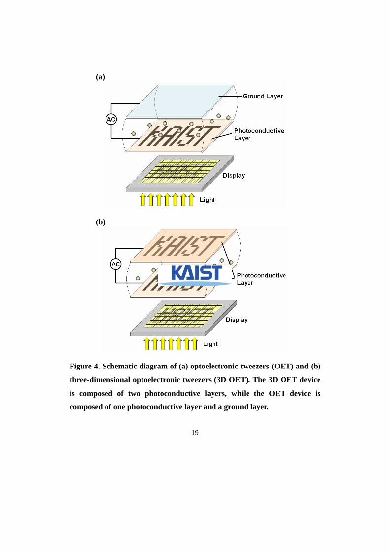
2.2. Design and fabrication
In the 3D OET device, the liquid layer containing microparticles is
sandwiched between two photoconductive layers (Figure 4(b)) differently from
the OET device composed of a photoconductive and a ground layer (Figure
4(a)). When an AC bias voltage is applied between two photoconductive layers,
the transmitted light beam forms virtual electrodes on the surfaces of the top
and the bottom photoconductive layer, resulting in an electric field gradient in
the liquid. This electric field gradient generates dipole moments of neutral
particles, which causes a DEP force for microparticle manipulation. The virtual
electrodes in 3D OET generate a 3-dimensional DEP cage to trap the particles
and focus them vertically using DEP forces. Consequently, we can manipulate
the vertically focused microparticles under the perfectly non-contact and
adsorption-free environments.
We used an indium tin oxide (ITO) layer as the transparent and
conductive layer for the ground. The photoconductive layer was comprised of
18
four layers: a 180 nm thick ITO layer, a 50 nm thick n+ doped hydrogenated
amorphous silicon (n+ a-Si:H) layer, a 800 nm thick intrinsic hydrogenated
amorphous silicon (intrinsic a-Si:H) layer, and a 20 nm thick silicon nitride
(SiNx) layer. Since the intrinsic a-Si:H has shorter carrier diffusion length and
higher optical absorption coefficient than crystalline silicon, it is a good
photoconductive material to make virtual electrode patterns of higher-
resolution[49, 50]. The 50 nm thick n+ a-Si:H layer was used to reduce the
contact resistance between the ITO layer and the intrinsic a-Si:H layer. The 20
nm thick SiNx layer was used to prevent electrolysis.
19
(a)
(b)
Figure 4. Schematic diagram of (a) optoelectronic tweezers (OET) and (b)
three-dimensional optoelectronic tweezers (3D OET). The 3D OET device
is composed of two photoconductive layers, while the OET device is
composed of one photoconductive layer and a ground layer.
20
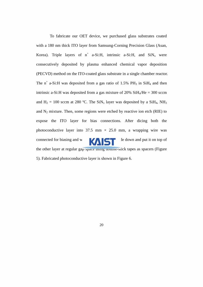
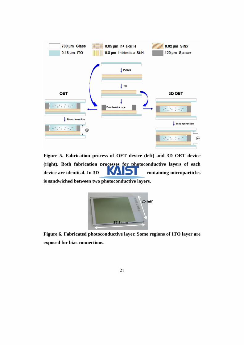
To fabricate our OET device, we purchased glass substrates coated
with a 180 nm thick ITO layer from Samsung-Corning Precision Glass (Asan,
Korea). Triple layers of n+ a-Si:H, intrinsic a-Si:H, and SiNx were
consecutively deposited by plasma enhanced chemical vapor deposition
(PECVD) method on the ITO-coated glass substrate in a single chamber reactor.
The n+ a-Si:H was deposited from a gas ratio of 1.5% PH3 in SiH4 and then
intrinsic a-Si:H was deposited from a gas mixture of 20% SiH4/He = 300 sccm
and H2 = 100 sccm at 280 ºC. The SiNx layer was deposited by a SiH4, NH3
and N2 mixture. Then, some regions were etched by reactive ion etch (RIE) to
expose the ITO layer for bias connections. After dicing both the
photoconductive layer into 37.5 mm × 25.0 mm, a wrapping wire was
connected for biasing and we turned one layer upside down and put it on top of
the other layer at regular gap space using double-stick tapes as spacers (Figure
5). Fabricated photoconductive layer is shown in Figure 6.
21
Figure 5. Fabrication process of OET device (left) and 3D OET device
(right). Both fabrication processes for photoconductive layers of each
device are identical. In 3D OET, the liquid layer containing microparticles
is sandwiched between two photoconductive layers.
Figure 6. Fabricated photoconductive layer. Some regions of ITO layer are
exposed for bias connections.
22
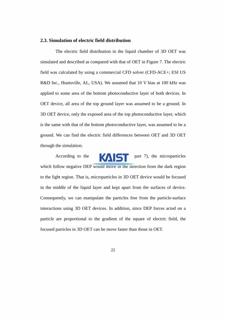
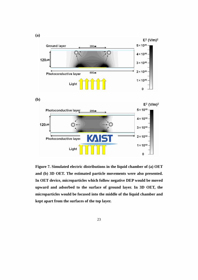
2.3. Simulation of electric field distribution
The electric field distribution in the liquid chamber of 3D OET was
simulated and described as compared with that of OET in Figure 7. The electric
field was calculated by using a commercial CFD solver (CFD-ACE+; ESI US
R&D Inc., Huntsville, AL, USA). We assumed that 10 V bias at 100 kHz was
applied to some area of the bottom photoconductive layer of both devices. In
OET device, all area of the top ground layer was assumed to be a ground. In
3D OET device, only the exposed area of the top photoconductive layer, which
is the same with that of the bottom photoconductive layer, was assumed to be a
ground. We can find the electric field differences between OET and 3D OET
through the simulation.
According to the simulation results (Figure 7), the microparticles
which follow negative DEP would move in the direction from the dark region
to the light region. That is, microparticles in 3D OET device would be focused
in the middle of the liquid layer and kept apart from the surfaces of device.
Consequently, we can manipulate the particles free from the particle-surface
interactions using 3D OET devices. In addition, since DEP forces acted on a
particle are proportional to the gradient of the square of electric field, the
focused particles in 3D OET can be move faster than those in OET.
23
(a)
(b)
Figure 7. Simulated electric distributions in the liquid chamber of (a) OET
and (b) 3D OET. The estimated particle movements were also presented.
In OET device, microparticles which follow negative DEP would be moved
upward and adsorbed to the surface of ground layer. In 3D OET, the
microparticles would be focused into the middle of the liquid chamber and
kept apart from the surfaces of the top layer.
24
2.4. Experimental
Experimental setup for 3D OET is shown in Figure 8. A 1.3 in
monochromatic LCD module (26.4 mm × 19.6 mm image area) from the
conventional projector (EMP-5300; Epson, Japan) was used in this research. It
was consisted of 800 × 600 pixel array with 33 µm pixel pitch. Its dimensions
were 42 mm in length, 40 mm in width, and 5 mm in thickness. The LCD
module was operated by the LCD driver circuit of the projector. The LCD
images were drawn by a standard presentation software program (Microsoft
PowerPointTM) or an interactive program we developed on a computer.
Plain polystyrene beads (PolySciences, PA, USA) were used for
particle manipulation in the condition of 20 V bias at 100 kHz. The sample was
prepared by dilution with deionized water (σ = 0.23 mS/m) to the final
concentration of about 2.5 × 10⁵ particles/mL. A sample droplet of 5-7 µL was
sandwiched between two photoconductive layers using double-stick tape as a
spacer, ensuring the liquid chamber of 120 µm thick. The bias voltage
produced from a function generator (MXG-9802A; Seowon Family Co., Korea
or AGF3022; Tektronix, USA) was applied.
We used two illuminations of the microscope: one for actuation and the
other for observation. The downside illumination with high intensity was used
25
for actuation, i.e., to create the image for virtual electrodes. The upside
illumination with low intensity was used for observation, because it was
difficult to see particles in a dark region without this upside illumination. The
movements of beads were observed and recorded using upright microscope
(Zeiss Axioskop 40; Carl Zeiss, Germany) with a digital camera (Coolpix5400;
Nikon, Japan). To investigate the effects of bias voltage and bead size on the
bad velocity, we recorded the bead movements and analyzed the video images
frame by frame using a analysis program that we made using MATLAB.
The microscopic pictures were taken without any image patterns of
LCD, because the optical observation of the beads in the dark region was
limited in the 3D OET device. To observe and capture the moved particles in
the dark region, we brightened whole area of LCD with a white full screen
after all manipulation experiments were finished.

26
Figure 8. Experimental setup for characterization of 3D OET. This
experimental setup was also utilized to OET device for comparing two
platforms (OET and 3D OET) with each other.
2.5. Results and discussion
Microscopic pictures on three different heights – bottom, middle, and
top – of the liquid chamber are shown in Figure 9. In the 3D OET device, the
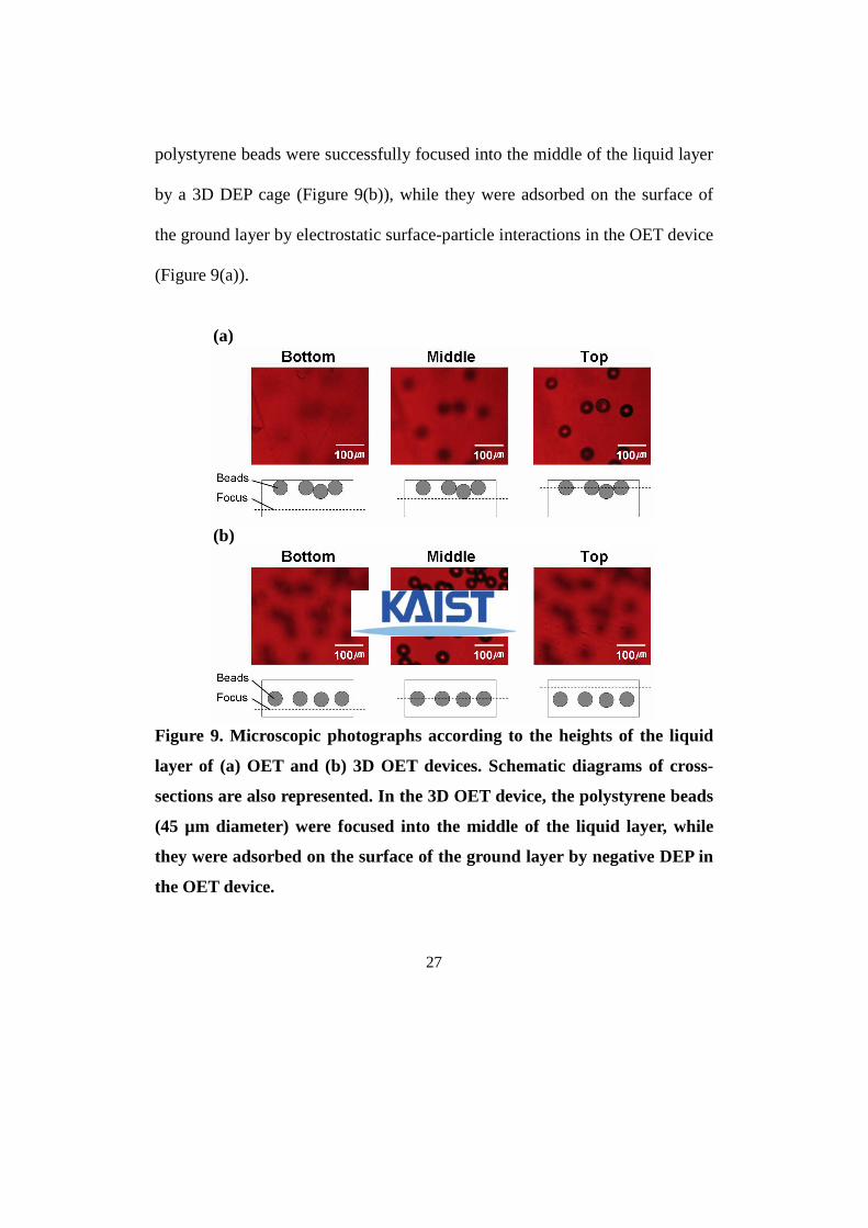
27
polystyrene beads were successfully focused into the middle of the liquid layer
by a 3D DEP cage (Figure 9(b)), while they were adsorbed on the surface of
the ground layer by electrostatic surface-particle interactions in the OET device
(Figure 9(a)).
(a)
(b)
Figure 9. Microscopic photographs according to the heights of the liquid
layer of (a) OET and (b) 3D OET devices. Schematic diagrams of cross-
sections are also represented. In the 3D OET device, the polystyrene beads
(45 µm diameter) were focused into the middle of the liquid layer, while
they were adsorbed on the surface of the ground layer by negative DEP in
the OET device.

28
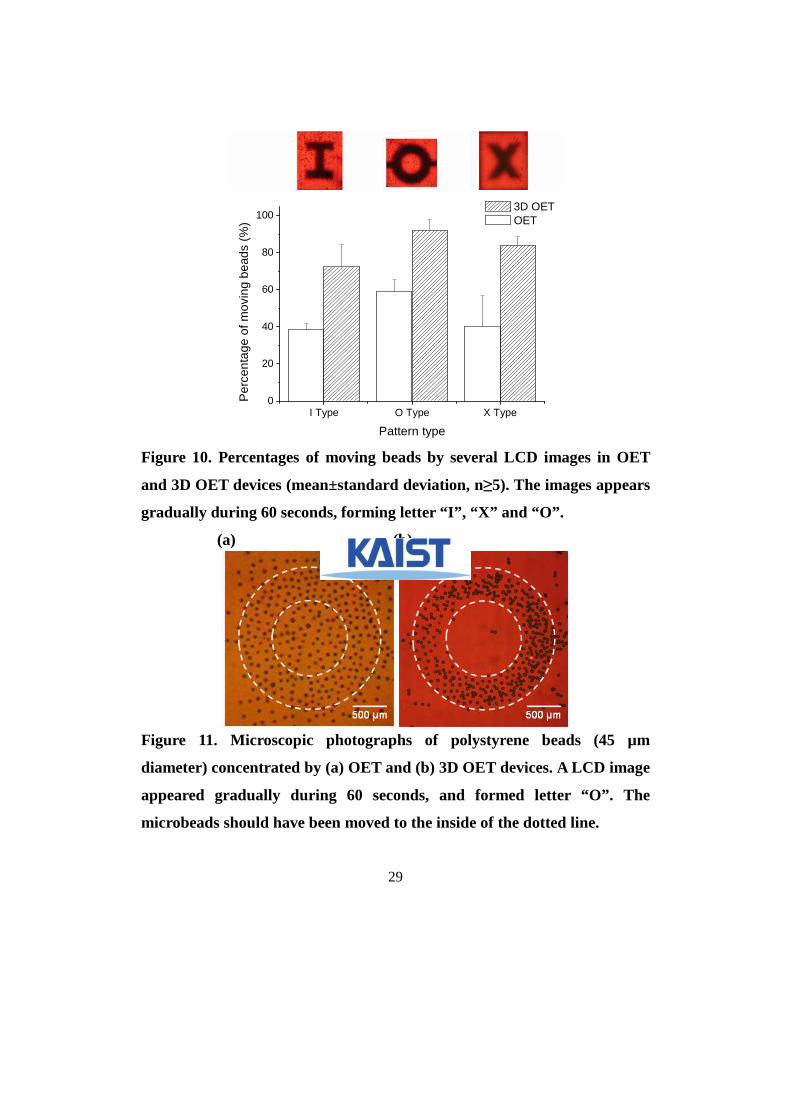
Since the number of moving particles speaks well for higher trapping
efficiency and adsorption-free particle manipulation of 3D OET, we have
compared the number of moving particles in 3D OET device with that in OET
device according to LCD images, bead sizes, and manipulation times. The
manipulation of 45 µm diameter size polystyrene beads was performed in the
condition of 20 V bias at 100 kHz. DI water whose measured electrical
conductivity is 0.23 mS/m was used as a buffer solution.
Figure 10 shows the number of moving particles by several LCD
images in OET and 3D OET devices. The image appears gradually during 60
seconds, forming letter “I”, “X” and “O”. We assumed that the microparticles
were uniformly spread out at the initial state, and calculated the percentages
using the number of particles moved by the images and the total number of
particles. The number of particles successfully moved by 3D OET was about
two times more than that of particles moved by OET. The microscopic
photographs of moved particles by LCD images forming letter “O” (the inside
of dotted lines is dark region) in OET and 3D OET devices are shown in Figure
11(a) and 11(b), respectively. The increased particle trapping efficiency of 3D
OET is shown.
29
I Type O Type X Type0
20
40
60
80
100 3D OET OET
Per
cent
age
of m
ovin
g be
ads
(%)
Pattern type
Figure 10. Percentages of moving beads by several LCD images in OET
and 3D OET devices (mean±standard deviation, n≥5). The images appears
gradually during 60 seconds, forming letter “I”, “X ” and “O”.
(a) (b)
Figure 11. Microscopic photographs of polystyrene beads (45 µm
diameter) concentrated by (a) OET and (b) 3D OET devices. A LCD image
appeared gradually during 60 seconds, and formed letter “O”. The
microbeads should have been moved to the inside of the dotted line.
30
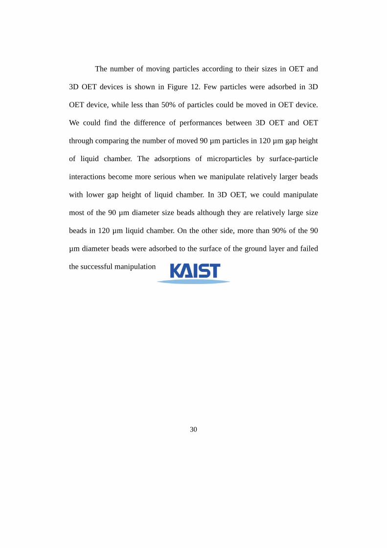
The number of moving particles according to their sizes in OET and
3D OET devices is shown in Figure 12. Few particles were adsorbed in 3D
OET device, while less than 50% of particles could be moved in OET device.
We could find the difference of performances between 3D OET and OET
through comparing the number of moved 90 µm particles in 120 µm gap height
of liquid chamber. The adsorptions of microparticles by surface-particle
interactions become more serious when we manipulate relatively larger beads
with lower gap height of liquid chamber. In 3D OET, we could manipulate
most of the 90 µm diameter size beads although they are relatively large size
beads in 120 µm liquid chamber. On the other side, more than 90% of the 90
µm diameter beads were adsorbed to the surface of the ground layer and failed
the successful manipulation in OET device.
31
15um 45um 75um 90um0
20
40
60
80
100 3D OET OET
Per
cent
age
of m
ovin
g be
ads
(%)
Bead diameter (µm)
Figure 12. Percentages of moving beads according to their sizes in OET
and 3D OET devices (mean±standard deviation, n≥5). The gap height of
liquid chamber was 120 µm and 20 V bias at 100 kHz was applied.
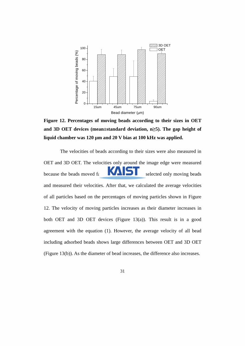
The velocities of beads according to their sizes were also measured in
OET and 3D OET. The velocities only around the image edge were measured
because the beads moved fastest there. Firstly, we selected only moving beads
and measured their velocities. After that, we calculated the average velocities
of all particles based on the percentages of moving particles shown in Figure
12. The velocity of moving particles increases as their diameter increases in
both OET and 3D OET devices (Figure 13(a)). This result is in a good
agreement with the equation (1). However, the average velocity of all bead
including adsorbed beads shows large differences between OET and 3D OET
(Figure 13(b)). As the diameter of bead increases, the difference also increases.
32
(a)
15 30 45 60 75 90
0
10
20
30
40
50 3D OET OET
Bea
d ve
loci
ty (
µm/s
)
Bead diameter (µm)
(b)
15 30 45 60 75 90
0
10
20
30
40
50 3D OET OET
Bea
d ve
loci
ty (
µm/s
)
Bead diameter (µm)
Figure 13. Bead velocities according to their sizes in OET and 3D OET
devices. (a) Bead velocities of moving beads (mean±standard deviation,
n≥20). (b) Average velocities of all beads including adsorbed beads. The
average velocities of all beads were calculated based on the percentages of
moving particles.
33
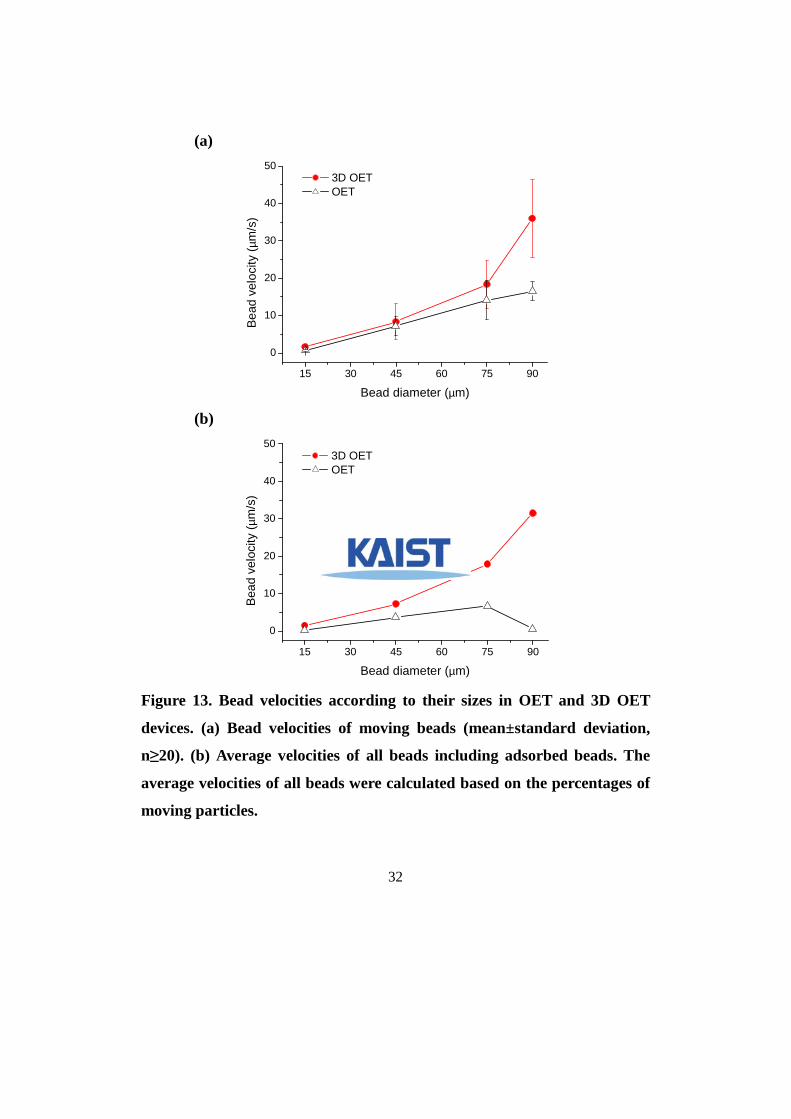
The result of time domain analysis is also described in Figure 14.
While the number of moving beads in OET decreases as time goes by, most of
the particles in 3D OET device were moved continuously without attachments.
The attached particles in OET induced strong electrostatic particle-particle
interactions and pulled other particles around them. This phenomenon
interferes with a continuous particle manipulation for a long time. It becomes a
very serious problem when a long-term particle manipulation is required.
0 90 180 270 360 4500
20
40
60
80
100
Per
cent
age
of m
ovin
g be
ads
(%)
Time (s)
3D OET OET
Figure 14. Percentages of moving beads according to the time in OET and
3D OET devices (mean±standard deviation, n≥5). While the number of
moving beads in OET decreases as time goes by, most of the particles in 3D
OET device were moved continuously without adsorptions.
34
Our 3D OET device is adapt to the lab-on-a-display platform which
uses no optical components. If a light is transmitted through a high N.A. lens
like a DMD OET and an iDEP platform, the light cannot be transmitted to both
two photoconductive layers since the lens can focus the light into only one
photoconductive layer. Consequently, the optical components such as objective
lens interfere with the normal operation of 3D OET. So, we used only lab-on-a-
display platform which uses an OET device on a LCD, resulting in direct light
transfer, for operating 3D OET.
2.6. Conclusion
In this work, 3D OET, which contains two photoconductive layers as a
pair, for 3D trapping and manipulation of microparticles has been developed.
We have successfully manipulated the polystyrene beads without attachments
using 3D OET on a LCD. The performances of 3D OET were compared with
those of OET according to several parameters; LCD images, bead sizes, and
manipulation times. The 3D OET shows higher particle trapping efficiency and
less particle adsorptions than a typical OET. However, the optical observation
of the beads in a dark region was limited when a thick photoconductive layer is
used as the upper photoconductive layer.
35
Chapter 3 Lens-integrated LCD-based Optoelectronic Tweezers
3.1. Introduction
Several types of OET platforms have been proposed since the
optoelectronic principles were reported in 2005[42, 47, 48]. The OET can be
classified in three categories based on the device for image generation: a DMD,
a projector and a LCD. Another classificatory criterion is whether optical
components such as objective lens and mirror structures need to be applied or
not (Table 1).
Since the DMD should reflect a light using micro-mirror array to make
an image and the projector, in general, flashes a largely diffracted image to
project on a large screen, the DMD OET and the image DEP applied a
projector ought to use the optical components for condensing, reflecting and
focusing an image. These optical components provide higher optical power and
smaller minimum pixel sizes by condensing original images, resulting in higher
manipulation performances. However, the optical components make their
practical usage difficult, and limit the portability because of their complex and
large structures. In lab-on-a-display which utilized a LCD for image generation,
no optical structures were constructed and the direct image transfer from LCD

36
to an OET device was used to obtain a large manipulation area, a simple
structure, and portability. However, the LCD images directly transmitted into
an OET device were diffracted and induced the blurred virtual electrodes on a
photoconductive layer, limiting its performances of microparticle manipulation
(Figure 15).
To overcome the limitations of each platform and to harmonize their
own advantages, here we propose a new OET platform using a LCD and a
condenser lens. In this study, we could construct a new LCD-based OET
system integrated with a condenser lens which offers a well-packaged structure.
This new platform is much simpler and easier to use than DMD OET and iDEP.
Additionally, it has much higher manipulation performances than lab-on-a-
display platform, comparable to DMD OET.
(a) (b)
Figure 15. Microscopic photographs of (a) an original LCD image and (b)
a blurred image on a photoconductive layer. The image blurring is
occurred by diffraction of the light.
37
3.2. Design and fabrication
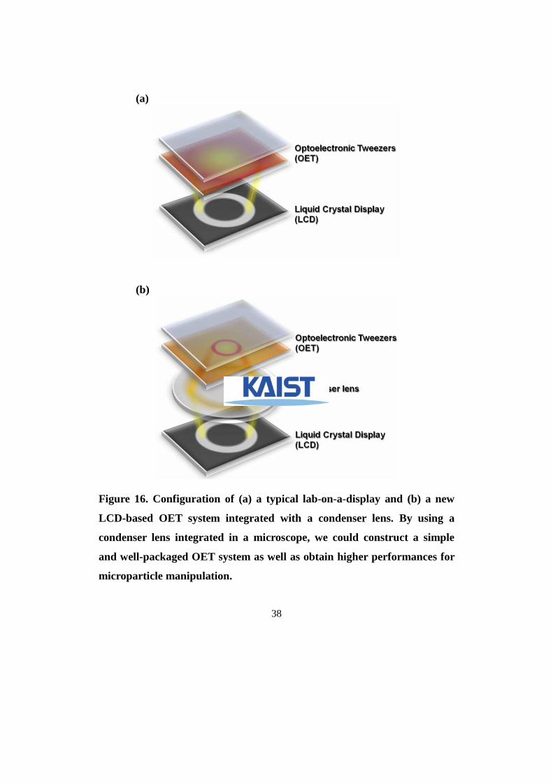
To prevent the diffraction of light in the lab-on-a-display, we utilized a
condenser lens positioned between an LCD and an OET device (Figure 16).
Although the optical component makes the OET system have higher
complexity in a general way, an integrated system which is thinner and simpler
than a typical OET system was constructed by using the direct light penetration
through LCD and the condenser lens integrated in a microscope. Through this
novel approach, we could obtain a high manipulation performance comparable
to a typical DMD OET platform as well as a well-integrated system as simple
as a typical lab-on-a-display platform.
The fabrication process of a photoconductive layer is the same with
Figure 5. In this study, we additionally fabricated a spacer using a
photolithography process for lower gap height (20 µm) of liquid chamber. The
device which has lower gap height was used for manipulation of smaller beads
or blood cells. Fabrication process of whole device including a
photoconductive layer and a spacer-patterned ground layer are shown in Figure
17.
38
(a)
(b)
Figure 16. Configuration of (a) a typical lab-on-a-display and (b) a new
LCD-based OET system integrated with a condenser lens. By using a
condenser lens integrated in a microscope, we could construct a simple
and well-packaged OET system as well as obtain higher performances for
microparticle manipulation.
39
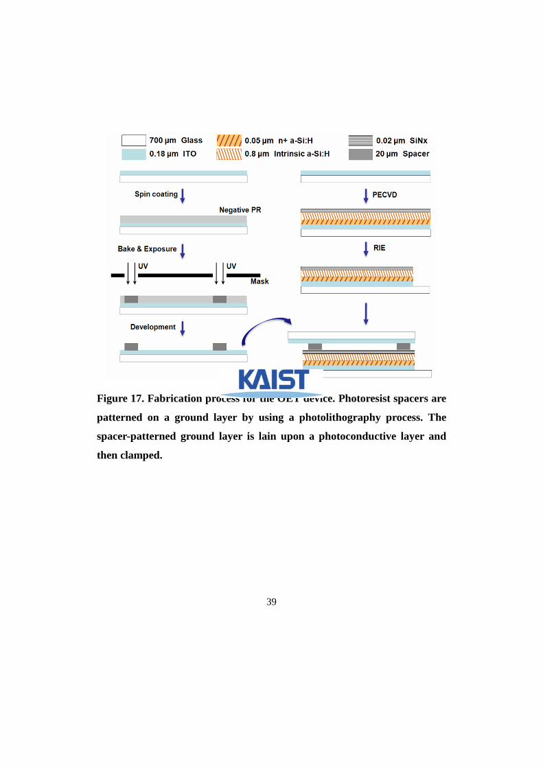
Figure 17. Fabrication process for the OET device. Photoresist spacers are
patterned on a ground layer by using a photolithography process. The
spacer-patterned ground layer is lain upon a photoconductive layer and
then clamped.
40
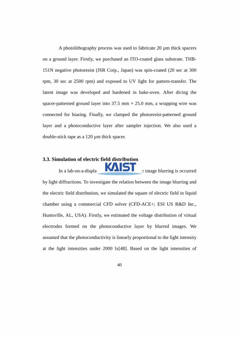
A photolithography process was used to fabricate 20 µm thick spacers
on a ground layer. Firstly, we purchased an ITO-coated glass substrate. THB-
151N negative photoresist (JSR Corp., Japan) was spin-coated (20 sec at 300
rpm, 30 sec at 2500 rpm) and exposed to UV light for pattern-transfer. The
latent image was developed and hardened in bake-oven. After dicing the
spacer-patterned ground layer into 37.5 mm × 25.0 mm, a wrapping wire was
connected for biasing. Finally, we clamped the photoresist-patterned ground
layer and a photoconductive layer after sampler injection. We also used a
double-stick tape as a 120 µm thick spacer.
3.3. Simulation of electric field distribution
In a lab-on-a-display and iDEP systems, the image blurring is occurred
by light diffractions. To investigate the relation between the image blurring and
the electric field distribution, we simulated the square of electric field in liquid
chamber using a commercial CFD solver (CFD-ACE+; ESI US R&D Inc.,
Huntsville, AL, USA). Firstly, we estimated the voltage distribution of virtual
electrodes formed on the photoconductive layer by blurred images. We
assumed that the photoconductivity is linearly proportional to the light intensity
at the light intensities under 2000 lx[48]. Based on the light intensities of
41
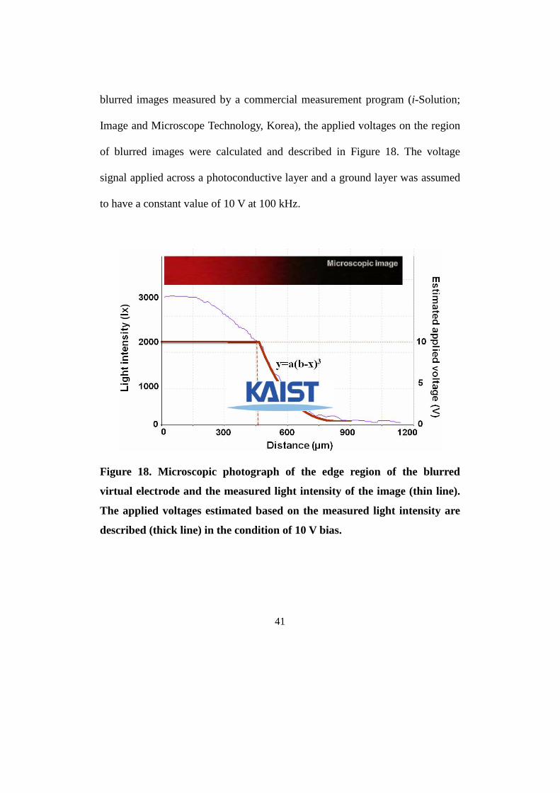
blurred images measured by a commercial measurement program (i-Solution;
Image and Microscope Technology, Korea), the applied voltages on the region
of blurred images were calculated and described in Figure 18. The voltage
signal applied across a photoconductive layer and a ground layer was assumed
to have a constant value of 10 V at 100 kHz.
Figure 18. Microscopic photograph of the edge region of the blurred
virtual electrode and the measured light intensity of the image (thin line).
The applied voltages estimated based on the measured light intensity are
described (thick line) in the condition of 10 V bias.
42
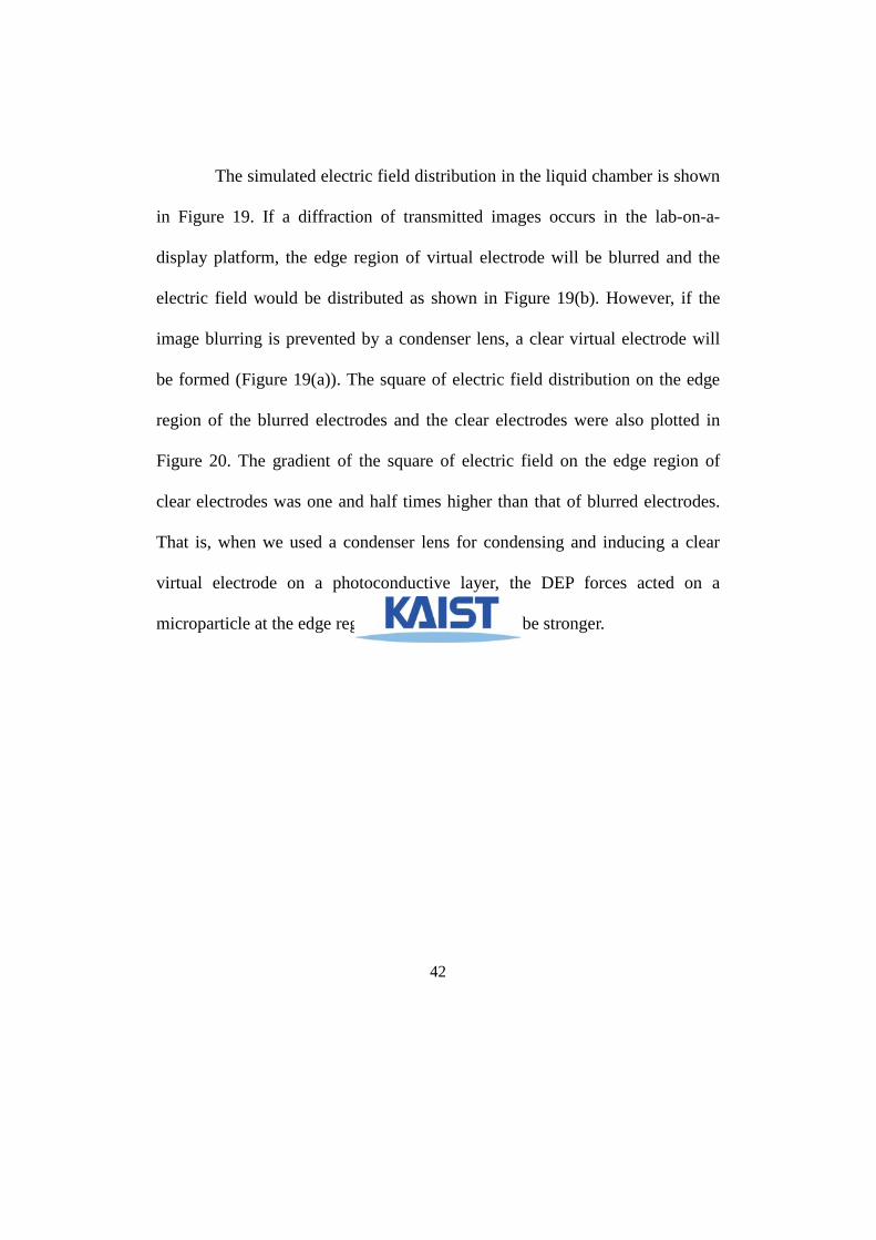
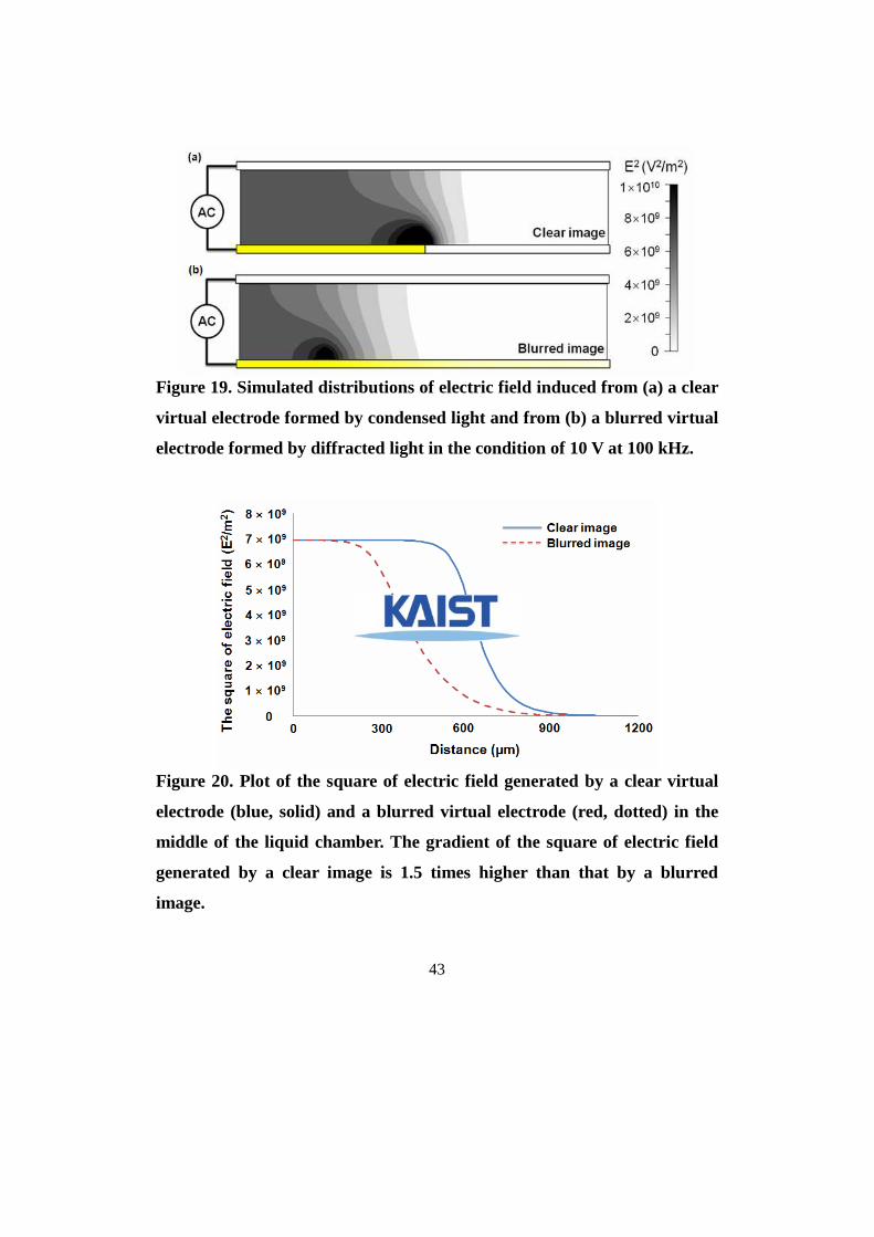
The simulated electric field distribution in the liquid chamber is shown
in Figure 19. If a diffraction of transmitted images occurs in the lab-on-a-
display platform, the edge region of virtual electrode will be blurred and the
electric field would be distributed as shown in Figure 19(b). However, if the
image blurring is prevented by a condenser lens, a clear virtual electrode will
be formed (Figure 19(a)). The square of electric field distribution on the edge
region of the blurred electrodes and the clear electrodes were also plotted in
Figure 20. The gradient of the square of electric field on the edge region of
clear electrodes was one and half times higher than that of blurred electrodes.
That is, when we used a condenser lens for condensing and inducing a clear
virtual electrode on a photoconductive layer, the DEP forces acted on a
microparticle at the edge region of electrode would be stronger.
43
Figure 19. Simulated distributions of electric field induced from (a) a clear
virtual electrode formed by condensed light and from (b) a blurred virtual
electrode formed by diffracted light in the condition of 10 V at 100 kHz.
Figure 20. Plot of the square of electric field generated by a clear virtual
electrode (blue, solid) and a blurred virtual electrode (red, dotted) in the
middle of the liquid chamber. The gradient of the square of electric field
generated by a clear image is 1.5 times higher than that by a blurred
image.
44
3.4. Experimental
A 0.5 in monochromatic LCD module (11.3 mm × 8.5 mm) from the
conventional projector (EMP-S4; Epson, Japan) was used in this research. It
was consisted of 800 × 600 pixel array with 14 µm pixel pitch. Its dimensions
were 19.2 mm in length, 21.8 mm in width, and 5 mm in thickness. The LCD
module was operated by the LCD driver circuit of the projector. The LCD
images were drawn by using an interactive control program we developed on a
computer.
We used two illuminations of the microscope: one for actuation and the
other for observation. The downside illumination with high intensity was used
for actuation, i.e., to create the image for virtual electrodes. The upside
illumination with low intensity was used for observation, because it was
difficult to see particles in a dark region without this upside illumination. The
maximum light intensity from the LCD was measured using an illuminance
meter (Illuminance Meter T-10M; Konica Minola Inc., Japan).
The LCD module was installed on the downside illumination of
upright microscope (Zeiss Axioskop 40; Carl Zeiss, Germany). The light
passed through LCD module was transmitted to a condenser lens (N.A. = 0.9)
of the microscope, condensing and focusing into a photoconductive layer of
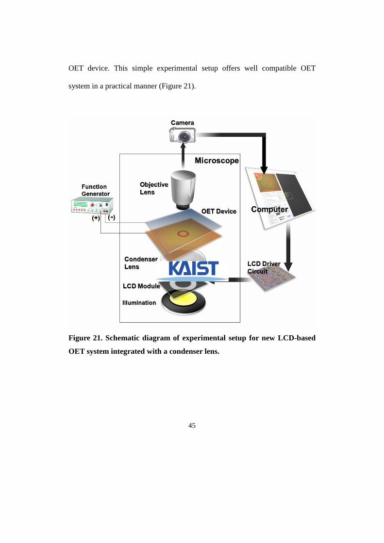
45
OET device. This simple experimental setup offers well compatible OET
system in a practical manner (Figure 21).
Figure 21. Schematic diagram of experimental setup for new LCD-based
OET system integrated with a condenser lens.
46
Plain polystyrene beads (PolySciences, PA, USA) were used for
particle manipulation in the condition of 20 V bias at 100 kHz. The sample was
prepared by diluting with deionized water (σ = 0.23 mS/m) to the final
concentration of about 2.5 × 10⁵ particles/mL. A sample droplet of 5-7 µL was
sandwiched between a photoconductive layer and a ground layer. When a 120
µm thick liquid chamber was required, we used a double-stick tape as a spacer.
If a 20 µm thick liquid chamber is needed to manipulate smaller beads (~15
µm), we used a ground layer that a photoresist spacer is fabricated on it.
We used fresh whole blood of a Sprague-Dawley rat as a blood sample.
Firstly, a 0.5 mL whole blood sample was taken from a healthy rat and kept in a
heparin-coated tube. To avoid coagulation of blood, we completed the
following procedure in a short period. After an isotonic glucose solution (8.5%
dextrose, 0.3% sucrose) was added to the blood sample, it was centrifuged and
the supernatant fluid was removed. The process was repeated two times for
washing and changing buffer solution. Finally, we obtained the blood cells 10:1
diluted with isotonic glucose solution (σ = 0.23 mS/m). In the condition of 7 V
bias at 200 kHz, we used the prepared blood sample for blood cell
manipulation.
47
3.5. Results and discussion
3.5.1. Simulation of Clausius-Mossotti factors
The simulation of Clausius-Mossotti factor should be performed before
the DEP experiment to acquire a proper AC voltage condition. The simulated
Clausius-Mossotti factors of polystyrene beads according to the AC frequency
are shown in Figure 22. The real part of Clausius-Mossotti factor of
polystyrene beads was simulated by using equation (2). The electrical relative
permittivity and conductivity of 15 µm polystyrene beads is 2.56 and 1.15
mS/m, respectively. When the AC frequency is higher than 200 kHz, the
polystyrene beads move by negative dielectrophoretic forces. On the other
hands, when the AC frequency is lower than 200 kHz, the polystyrene beads
show positive dielectrophoretic motions with the media conductivity larger
than 100 mS/m.

48
Figure 22. The simulated real part of Clausius-Mossotti factor of a 15 µm
diameter size polystyrene bead in mediums with conductivities of 1 S/m,
100 mS/m, 10 mS/m, 1 mS/m, and 0.1 mS/m. The relative permittivity and
conductivity of the polystyrene bead is assumed to be 2.56 and 1.15 mS/m,
respectively.
49
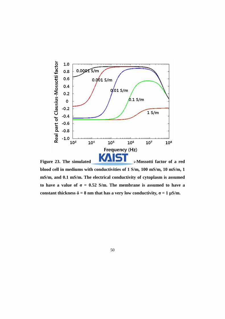
The simulation of frequency-dependent Clusius-Mossotti factors of
erythrocytes was also performed (Figure 23). In the case of the erythrocytes,
they were represented by a single-shell model[51]. In practice, the biconcave
erythrocyte model has been used, but the spherical model with an effective
radius of erythrocytes used in this work for simplification. The electrical values
of erythrocytes which have been extensively used in the literature were
utilized[52-55]. The cytoplasm is a physiological saline solution with a protein
volume fraction of 0.26, relative electrical permittivity εr = 50 and conductivity
σ = 0.52 S/m. The membrane is represented by a shell of constant thickness δ =
8 nm that has a very low conductivity σ = 1 µS/m and a relative permittivity εr
= 5. The cell is immersed in an external media whose relative permittivity εr =
78.
The real part of Clausius-Mossotti factor of erythrocytes is switched
from negative to positive at the AC frequency less than 10 MHz. The switching
frequency increases as the AC frequency increases. However, when the
conductivity of media is larger than 1 S/m, the negative dielectrophoretic
forces are acted on the erythrocytes at the all frequency ranges. On the other
hands, the conductivity of media is smaller than 1 mS/m, the positive DEP is
always shown.
50
Figure 23. The simulated real part of Clausius-Mossotti factor of a red
blood cell in mediums with conductivities of 1 S/m, 100 mS/m, 10 mS/m, 1
mS/m, and 0.1 mS/m. The electrical conductivity of cytoplasm is assumed
to have a value of σ = 0.52 S/m. The membrane is assumed to have a
constant thickness δ = 8 nm that has a very low conductivity, σ = 1 µS/m.
51
3.5.2. Condensation of LCD image
Figure 24 shows two LCD images; one is an original LCD image and
the other is a condensed image focused on a photoconductive layer. We could
prevent the image blurring by light diffraction using a condenser lens. The
magnification and N.A. of the condenser lens are ×5 and 0.9, respectively.
Consequently, we could get five times smaller minimum pixel size (2.8 µm)
than original LCD pixel size (14 µm). The minimum pixel size can be smaller
if we use another LCD module which has smaller pixels or another lens
structure which has higher magnification. However, the manipulation area of
this lens-integrated LCD OET system (3.8 mm2) became much smaller than
that of a lab-on-a-display which directly uses transferred images from LCD
without any optical components. We cannot get a wide manipulation area with
smaller minimum pixel size because the manipulation area decreases as the
minimum pixel size decreases.

52
Figure 24. Microscopic photographs of (a) an original LCD image and (b)
a condensed image on a photoconductive layer. The image blurring is
prevented by a condenser lens.
3.5.3. Polystyrene bead manipulation
The bead velocities according to their diameter in our new LCD OET
system and in a typical lab-on-a-display system are shown in Figure 25. The
measured bead velocity in new LCD OET platform integrated with a condenser
lens was much higher than that in a typical lab-on-a-display platform. In a
typical LCD OET platform, lab-on-a-display, manipulation of microbeads
smaller than 18 µm diameter size was almost impossible in the conditions of 20
V bias at 100 kHz. On the other hand, we could successfully trap and
manipulate 15 µm diameter size beads using a new LCD-based OET platform
integrated with a condenser lens to prevent a blurring effect by light
diffractions (Figure 26). The maximum velocity of 15 µm diameter size beads
was about 8 µm/s in 120 µm height liquid chamber.

53
15 30 45 60 75 90
0
30
60
90
120 Gap height : 120 µm Condenser-LCD Only LCD
Bea
d ve
loci
ty (
µm/s
)
Bead diameter (µm)
Figure 25. Bead velocities according to their sizes in a new LCD-based
OET system and a lab-on-a-display (mean±standard deviation, n≥20). The
LCD-Condenser OET system shows higher manipulation performances
than the lab-on-a-display platform which uses only LCD without any lens
structures.
Figure 26. The captured photographs after parallel manipulation of 15 µm
polystyrene beads. The maximum velocity of the microbeads is 8 µm/s in
the condition of 20 V at 100 kHz.
54
According to those experimental results, we could find that the blurred
virtual electrodes induced from the diffracted LCD image in lab-on-a-display
limit the effective microparticle manipulation. We already confirmed that the
square of electric field gradient induced from a clear virtual electrode is one
and a half times larger than that induced from a blurred virtual electrode
through the simulation study (Figure 22). We also measured the maximum light
intensity of images transmitted to a photoconductive layer in each case. When
we used a lens to condense the light from LCD, the optical power was
measured ten times stronger than when we did not use any optical components
for condensing LCD images. These factors would affect the improvement of
performances of the new LCD OET system.
However, the polystyrene beads smaller than 10 µm (diameter) did not
move even when we used the new LCD OET for particle manipulation. To
solve this problem, we lowered the gap height of liquid chamber of OET
device from 120 µm to 20 µm. To investigate the relation between the height of
liquid chamber and the induced dielectrophoretic forces, other experimental
conditions were fixed and only the ground layer was changed to the 20 µm
thickness spacer-patterned ground layer. The measured bead velocities are
shown in Figure 27. We could successfully manipulate 8 µm diameter size

55
polystyrene beads with 11 µm/s average velocity in 20 µm height liquid
chamber. Larger dielectrophoretic force would be generated since the electric
field gradient increases as the gap height of liquid chamber decreases.
Accordingly, smaller beads may also be trapped and manipulated if an OET
device which has lower liquid chamber is used.
8 10 12 14 16
0
10
20
30
Gap height 20 µm 120 µm
Bead diameter (µm)
Bea
d ve
loci
ty (
µm/s
)
Figure 27. Bead velocities according to their sizes in 20 µm and 120 µm
height liquid chambers of OET device (mean±standard deviation, n≥20).
As the height of liquid chamber decreases, the optically-induced
dielectrophoretic force increases.
56
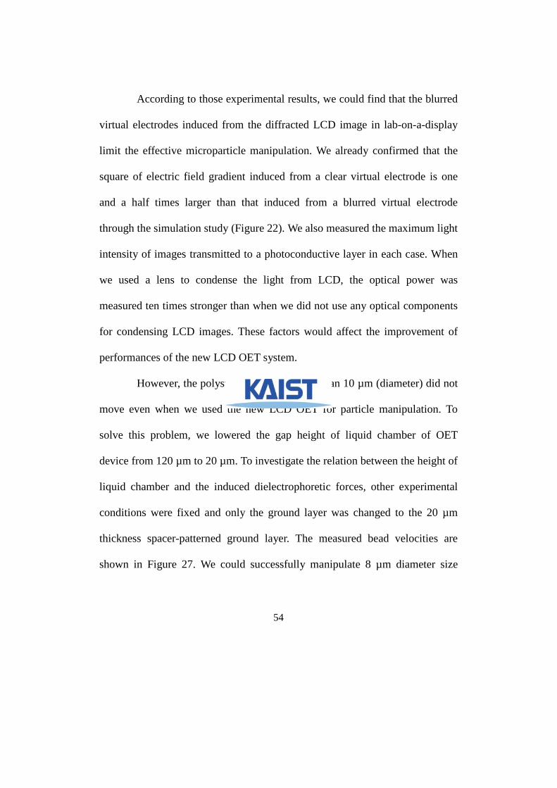
We trapped a 10 µm diameter size bead using a virtual DEP cage and
go through a maze constructed by virtual electrodes (Figure 28). The gap
height of liquid chamber was 20 µm and the applied voltage was 20 V bias at
100 kHz. The measured maximum velocity of the bead was 16 µm/s. After 3
minutes, we could find the way to thread the maze. This interactive
manipulation of polystyrene beads was performed by using an interactive
control program we developed. We can interactively draw and move an image,
namely a virtual electrode, as seeing a real-time microscopic movie through the
interactive control program.
Figure 28. Interactive manipulation of a polystyrene bead for threading a
maze constructed by optically-induced virtual electrodes.
57
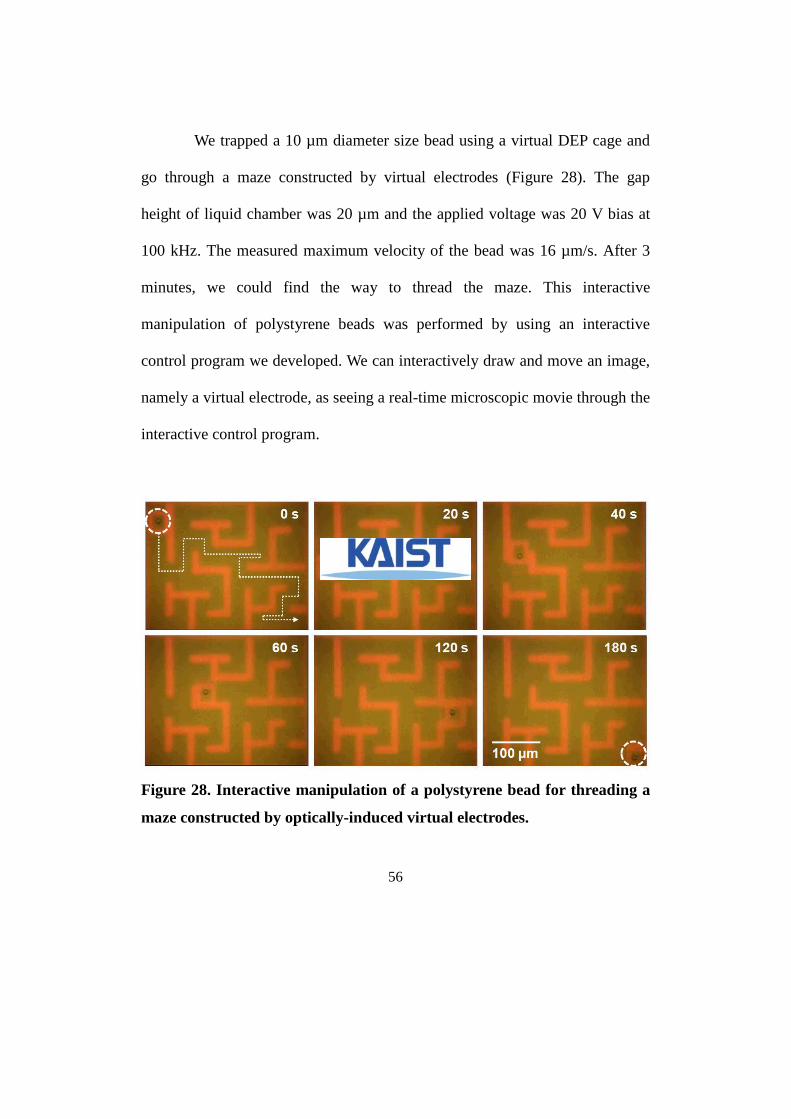
3.5.4. Blood cell manipulation
We have successfully concentrate blood cells using optically-induced
positive DEP (Figure 29). A number of blood cells were transported to the
bright (red) area of the LCD image forming a word “KAIST” during 60
seconds. When operating voltage was applied, red blood cells were arranged in
the direction of parallel to the electric field direction. Some red blood cells
were aggregated by dipole interactions.
Figure 30 demonstrates the trapping and transporting of individual red
blood cells using optically-induced virtual electrode array. One to three red
blood cells were trapped in each light spot by positive DEP under the voltage
condition of 7 V at 200 kHz. By programming the LCD image, a column of the
array could be selected and moved. The moving column successfully
transported the trapped red blood cells individually in the upper direction.
58
(a) (b)
Figure 29. Concentration of red blood cells using a LCD image forming a
word “KAIST” during 60 seconds. (a) Voltage is not applied. (b) Voltage is
applied.
Figure 30. Parallel manipulation of red blood cells trapped in a virtual
electrodes array. One to three cells are trapped in each light spot by
positive DEP. A selected column of the array moves in the upper direction,
transporting red blood cells.
59
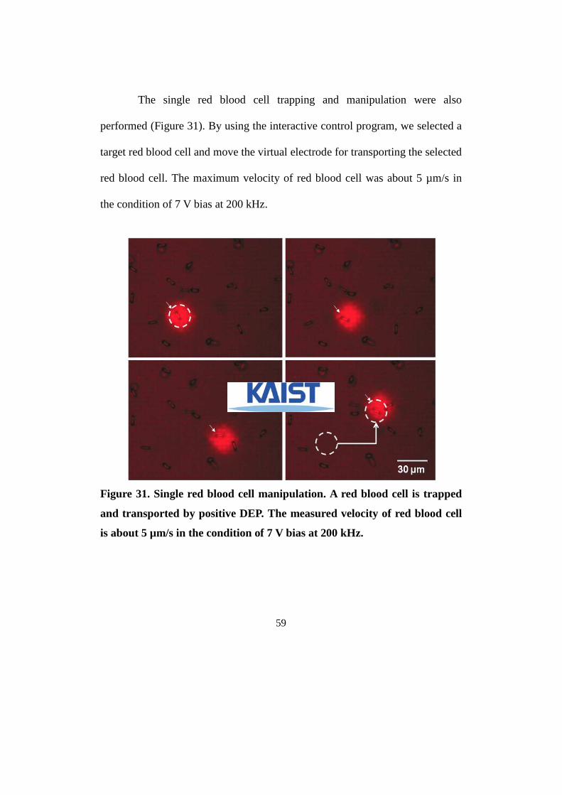
The single red blood cell trapping and manipulation were also
performed (Figure 31). By using the interactive control program, we selected a
target red blood cell and move the virtual electrode for transporting the selected
red blood cell. The maximum velocity of red blood cell was about 5 µm/s in
the condition of 7 V bias at 200 kHz.
Figure 31. Single red blood cell manipulation. A red blood cell is trapped
and transported by positive DEP. The measured velocity of red blood cell
is about 5 µm/s in the condition of 7 V bias at 200 kHz.
60
Figure 32 demonstrates selection and manipulation of single white
blood cell. We could find a target white blood cell among many red blood cells
through real-time movie on a monitor. After finding and selecting the target
white blood cell, a virtual dielectrophoretic tweezers was generated and we
dragged the selected white blood cell out from many unwanted red blood cells.
These processes were performed by using the interactive control program in
the same voltage condition and a light spot whose diameter is about 6 µm was
used for trapping a white blood cell. If the size of light spot increased, the red
blood cells moved to the virtual electrode by positive DEP interfere with the
selection and transport of a white blood cell.
61
Figure 32. Selection and manipulation of a single white blood cell among
many red blood cells in the condition of 7 V bias at 200 kHz. The minimum
size of light spot for trapping a white blood cell is about 6 µm.
62
3.6. Conclusion
In this paper, we have developed a new LCD-based OET system which
uses a LCD and a condenser lens for projecting an image into an OET device.
By using the condenser lens integrated in a microscope, we could successfully
construct a simple integrated OET system. Bead velocities according to their
size were measured using this new platform, comparing with a typical lab-on-
a-display platform. The bead velocities under different gap height of liquid
chamber in OET device were measured. We could also manipulate blood cells
using this new platform.
Our new LCD OET provides much higher performances than a typical
lab-on-a-display, comparable to DMD OET, by preventing the image blurring
induced from light diffraction using condenser lens. Additionally, this new
platform is much simpler and easier to use than typical OET platforms which
use some optical components in a practical manner. This new LCD-based OET
system using a condenser lens and a LCD may be a usable integrated system
for optoelectronic manipulation of microparticles including live cells because
of its simple structures and high performances.
63
Chapter 4 Conclusions
In this research, we have demonstrated two approaches for
enhancement of typical OET platforms; 3D OET and lens-integrated LCD OET.
First, the 3D OET composed of two photoconductive layers was successfully
utilized to focus microparticles into the middle of the liquid chamber using
negative DEP. Consequently, we could keep the microparticles apart from the
surface of device, preventing adsorptions by electrostatic surface-particle
interactions in OET device. We compared the performances of a 3D OET
device with those of a typical OET device according to several parameters;
LCD images, bead sizes and manipulation times. In 3D OET device, about
90 % of target particles were successfully manipulated continuously for a long
time (t ≥ 450 sec), while about 50 % of particles were adsorbed to the device
surface or focused out by vertical forces in OET device. In the case of 90 µm
diameter beads in 120 µm gap height of liquid layer, about 95 % of them were
adsorbed. If we use relatively low gap height of liquid chamber, the gradient of
the square of electric field which is proportional to the DEP forces would be
increased, but the adsorptions of manipulated particles would be also increased.
Therefore, we need to consider the mutual exclusion before we decide the gap
64
height of liquid chamber when we use the OET for particle manipulation.
However, when we used the 3D OET, all particles could be manipulated
without adsorptions regardless of their size and the gap height of liquid
chamber. The higher particle trapping efficiency and less particle adsorptions
of 3D OET make it more compatible tools for manipulation of microparticles
including live cells and polymer beads.
However, some limitations which need to be conquered are remained.
The optical observation of the beads in a dark region was limited when a thick
photoconductive layer is used as the upper photoconductive layer. Additionally,
the 3D OET device is only adapted to the lab-on-a-display platform which uses
no optical components, resulting in direct light transfer, because a high N.A.
lens makes the transmitted light to be focused into only one photoconductive
layer. However, as we mentioned previously, the image blurring is occurred in
the lab-on-a-display, resulting in smaller DEP forces for particle manipulation.
To overcome the drawbacks, we can utilize a new display device which can
project the image into both two photoconductive layers of 3D OET. Two light
sources can be also applied; one is for inducing the virtual electrodes on the
upper photoconductive layer and the other is for inducing them on the bottom
one. If the double-light source structure can be constructed, the ‘real’ three-
65
dimensional particle manipulation, not only focusing but also control of
vertical positions of each particle, may also be possible.
Second, we have also developed a new LCD-based OET system using
a condenser lens for preventing light diffractions and providing higher
manipulation performances and virtual electrode resolution. By using an LCD
for image generation and a condenser lens integrated in a microscope, we could
obtain not only higher particle manipulation performances, but also a simple
and well-packaged OET system. An image blurring was completely reduced by
using the condenser lens whose magnification and N.A. are ×5 and 0.9,
respectively. The minimum pixel size of virtual electrode was 2.8 µm when we
use an LCD module whose pixel size is 14 µm. Because of the clear and
smaller virtual electrodes, the optically-induced DEP forces were increased
about 1.5 times. Additionally, in the lens-integrated LCD OET, the
condensation of light by the condenser lens offered optical power 10 times
stronger than the conventional lab-on-a-display platform. When the gap height
of liquid chamber was lowered from 120 µm to 20 µm, the electric field
gradient was increased significantly and we could manipulate smaller
microbeads (8 µm diameter polystyrene beads) with 11 µm/s average velocity
using the optically-induced DEP. We could also observe an electro-osmosis of
66
5.4 µm diameter fluorescent microbeads with a certain voltage condition. It
shows a possibility of our LCD OET platform for AC-electro-osmotic
nanoparticle manipulation. An interactive control program was also developed
and demonstrated for manipulation of polystyrene beads and blood cells.
Selection and transport of a single red blood cell and a single white blood cell
were successfully demonstrated using this platform.
In the case of blood cells, dielectrophoretic aggregation and positive
dielectrophoretic movements of them interfered the effective single cell
manipulation and the measurement of dielectrophoretic velocity. To prevent the
aggregation of blood cells by positive DEP and electrostatic aggregation, we
needed to minimize the size of light spot which is the same with the size of
virtual electrode. If we could utilize negative DEP for blood cell manipulation,
single cell trapping and manipulation would be easier. For inducing the
negative DEP of biological cells, higher conductivity of the buffer media is
required. To apply the buffer media which has higher conductivity for cell
manipulation without electrolysis, the conductivity of photoconductive layer
should be larger than that of the buffer solution. However, in the case of our
OET device which is composed of hydrogenated amorphous silicon, the
photoconductivity is too low to apply high conductive buffer media such as
67
phosphate buffered saline (PBS) solution. If we utilize a material which has
higher photoconductivity, the negative dielectrophoretic manipulation of
biological cells without additional processes for buffer change will be possible.
The particle adsorptions by vertical DEP forces in OET device was also a
problem. Of course, the adsorptions between manipulated particles and device
surfaces were reduced by using a 3D OET device in chapter 2. However, we
could not utilize the 3D OET device to the lens-integrated LCD OET platform.
It was caused by the light focused into only one photoconductive layer by the
condenser lens as we mentioned above. Because we use the condenser lens of
microscope for focusing LCD images, the background light for observation of
microparticles in the OET device was intercepted. It can also be a problem of
power our integrated LCD OET platform, when we observe the manipulated
particles using an objective lens of high magnifying power.
However, we could easily set up the lens-integrated LCD OET system
as positioning an LCD module and an OET device on the light source and on
the stage of a microscope, respectively. In addition, high performance for
microparticle manipulation was obtained with the simple structure. The
interactive control program which we developed was also helpful to manipulate
single cells or microbeads interactively as seeing the target particles through a

68
computer monitor. The higher performances and well-integrated structures of
our new OET system can make it a wide usable platform for optoelectronic
manipulation of microparticles including live cells in many biological
applications.
69
Summary in Korean
본 연구에서는 미세입자 및 혈액세포를 자유자재로 구동하기
위한 액정 디스플레이 (LCD; Liquid crystal display) 기반의 새로운
광전자집게 (OET; Optoelectronic tweezers)를 제안하였다.
광전자집게란 움직이는 디스플레이 영상을 광전도성 층에
조사함으로써 가상의 전극을 형성시키고, 이로 인해 발생한 불균일한
전기장을 이용하여 유전영동 (DEP; Dielectrophoresis)을 유도,
미세입자를 자유자재로 구동하는 기술이다. 이러한 광전자집게는
세포와 같은 미세입자들을 제어하여 여러 가지 생물학적 또는
화학적 실험을 진행하는데 매우 유용하다. 그러나 기존의
광전자집게의 경우 2 차원 상에서 형성되는 가상 전극을 이용하기
때문에 미세입자의 수직 운동을 제어할 수 없다는 한계가 있다.
그러므로 수직방향으로 작용하는 유전영동력에 의해 현미경
초점으로부터 벗어나게 되는 현상이나 정전기적 표면-입자 반응에
의한 미세입자의 표면 흡착 현상 때문에 미세입자의 포획 및 구동
효율이 감소하는 문제점이 존재하였다.
70
본 연구에서는 이러한 문제점을 해결하기 위하여 두 개의
광전도성 층으로 이루어진 3 차원 광전자집게 (3D OET; Three-
dimensional optoelectronic tweezers)를 제안하였다. 3차원 광전자집게는
하나의 광전도성 층 및 하나의 투명한 접지전극 층을 사용하는
기존의 광전자집게와 달리, 두 개의 광전도성 층을 이용하기 때문에
미세입자를 중심으로 상하로 형성되는 가상의 전극을 이용할 수
있다. 이 때 상하로 형성된 가상의 전극은 음의 유전영동력을
발생시켜 3 차원 상에서 미세입자를 포획할 수 있도록 하며 이로
인해 미세입자의 흡착과 같은 현상이 제거되며, 결과적으로
미세입자의 포획 및 구동 효율이 크게 향상될 수 있다.
3 차원 광전자집게를 형성하는 광전도성 층은 투명한 전도성
물질인 ITO (Indium tin oxide)가 코팅된 유리웨이퍼 위에 PECVD
(Plasma enhanced chemical vapor deposition)를 이용하여 접촉 저항
감소를 위한 n 형의 도핑된 비정질 실리콘 (n+ doped amorphous silicon),
광전도성 물질인 진성의 비정질 실리콘 (intrinsic amorpous silicon) 및
샘플의 전기분해를 막기 위한 질화 실리콘 (silicon nitride)을 차례로
증착시킨 후, ITO 에 전압인가를 하기 위한 일부 영역을 RIE (Reactive

71
ion etch)를 이용하여 식각함으로써 제작되었다. 이렇게 제작된 두
개의 광전도성 층을 미세입자가 들어있는 미세유체 방울을 사이에
두고 서로 마주보도록 포개어 3 차원 광전자집게를 완성하였다.
미세입자를 구동하기 위한 영상은 액정 디스플레이를 통해
조사되었으며, 렌즈가 없는 랩온어디스플레이(Lab-on-a-display)
플랫폼을 이용함으로써 상하 두 개의 광전도성 층에 똑 같은 모양의
가상의 전극을 형성시킬 수 있었다.
3 차원 광전자집게를 이용한 미세입자의 구동 속도 및 구동
효율을 측정한 후 기존의 광전자집게와 비교한 결과, 3 차원
광전자집게에서 음의 유전영동력에 의하여 유체 층의 중심으로
포커싱된 미세입자의 경우 기존의 광전자집게에서보다 구동 속도 및
구동효율이 증가함을 알 수 있었다. 특히 기존의 광전자집게에서는
절반 가량의 미세입자들이 흡착되었던 반면, 3차원 광전자집게에서는
그러한 흡착현상이 거의 완벽하게 제거됨으로써 90%이상의 매우
높은 구동효율을 얻어 낼 수 있었다. 이러한 3 차원 광전자집게는
완벽히 비접촉(non-contact)된 구동환경을 제공함으로써 흡착이나
72
외부에서 가해지는 힘에 특히 민감한 생물학적 세포의 구동에 매우
적합하다.
광전자집게는 영상을 조사하는 장치의 종류 및 렌즈의 유무에
따라 다양한 종류가 존재한다. 지금까지 개발된 광전자집게
플랫폼으로는 디지털 미세거울 장치 (DMD; Digital micromirror
device)를 이용한 DMD OET, 프로젝터를 이용한 iDEP (image DEP),
액정 디스플레이를 이용한 lab-on-a-display가 있다. DMD OET 와
iDEP 의 경우에는 빛이 반사되어 분산되는 형식의 영상표시장치를
이용하기 때문에, 광전도성 층에 정확하게 상을 맺히게 하기 위해서
복잡한 렌즈 및 거울 장치를 필요로 한다. 반면에 lab-on-a-display의
경우에는 복잡한 광학계 없이 액정 디스플레이 위에 바로
광전자집게 장치를 위치 시킴으로써 매우 단순한 구조와 휴대성
(portability)을 갖추고 있다. 이는 빛을 반사시키는 디지털
미세거울장치나 프로젝터와 달리 빛을 통과시킴으로써 영상을
만들어 내는 액정 디스플레이 특징 때문에 가능한 것이다. 그러나
lab-on-a-display 의 경우에는 렌즈와 같은 광학장치가 없기 때문에
빛이 분산되는 현상이 발생하고 이로 인해 흐릿한 영상이
73
광전자집게에 맺혀 흐릿한 가상의 전극이 형성되었고, 그로 인해
미세입자를 구동하기 위한 성능이 다른 장치에 비해 현저히
감소하는 문제점이 있었다.
본 연구에서는 사용하기 편리하고 단순한 구조를 지닌 동시에
뛰어난 미세입자 구동성능을 가진 새로운 광전자집게 플랫폼으로서
렌즈가 통합된 새로운 액정 디스플레이 기반의 광전자집게 시스템을
제안하였다. 본 연구에 따른 새로운 플랫폼은 빛을 통과시켜 상을
맺히게 하는 액정 디스플레이의 특성을 이용하여, 단순히 현미경의
광원 위에 액정 디스플레이를 올려놓음으로써 현미경에 통합되어
설치된 집광렌즈를 거쳐 재물대 위의 광전자집게 장치에 정확하게
상이 맺히도록 하는 원리를 이용하였다. 이러한 단순한 구조의 통합
플랫폼은 현미경과 액정 디스플레이, 광전자집게 장치만으로 우수한
구동성능을 보이며 사용자 입장에서 그 실용성이 매우 뛰어나다고
볼 수 있다.
본 논문에서 사용한 광전자집게 장치는 앞서 서술한 것과
똑같은 방식으로 제작된 광전도성 층과 ITO 로 만들어진 접지전극
층으로 이루어져 있다. 액정 디스플레이는 최소한의 가상 전극

74
크기를 얻기 위해 픽셀 크기가 14 µm 인 프로젝터용 흑백 액정
디스플레이를 사용하였으며, 현미경에 통합된 집광렌즈는 개구수가
0.9, 배율이 5 배인 것을 사용하였다. 이로서 우리는 최소 2.8 µm 의
크기를 지닌 가상 전극을 광전도성 층에 뚜렷하게 형성되도록 할 수
있었다. 이는 기존의 lab-on-a-display에 비해 약 100 배 정도 더 작은
크기이다. 뚜렷한 영상에 의한 가상의 전극과 흐릿한 영상에 의한
가상의 전극에 의해 각각 형성되는 전기장의 기울기 및
유전영동력을 시뮬레이션을 통해 확인한 결과 영상이 뚜렷할 경우
약 1.5 배 정도 그 크기가 컸다. 실제 광전자집게에 조사되는 빛의
세기를 측정한 결과 렌즈를 이용하였을 때 빛의 세기는 약 10 배
정도 크게 측정되었다. 미세입자를 구동한 결과 렌즈를 사용한
새로운 플랫폼에서는 구동 속도가 10 배 이상 빠르게 측정된 것도
앞서 서술한 몇 가지 요소들이 미세입자에 작용하는 유전영동력의
크기에 영향을 미쳤기 때문일 것이다. 뿐만 아니라 광전자집게의
유체 층의 높이가 유전영동력에 미치는 영향에 관한 실험도
수행하였다. 유체 층의 높이가 낮아질수록 더 작은 미세입자를 더
75
빠르게 구동할 수 있었다. 이는 유체 층의 높이가 낮아질수록 전기장
기울기가 커지고 따라서 유전영동력도 증가하기 때문이다.
본 연구에서는 위의 새로운 액정디스플레이 기반의
광전자집게 시스템에 미세입자의 인터랙티브한 제어를 위한 플래쉬
기반의 컨트롤 프로그램을 적용하여 미세입자 및 혈액세포의
인터랙티브한 구동에 성공하였다. 혈액은 쥐로부터 채취하여
원심분리 한 후 상층액을 제거하고 등장성 용액으로 10:1 로
희석시켜준 것을 최종적으로 사용하였다. 인터랙티브 컨트롤
프로그램을 이용하면 현미경과 카메라를 통해 컴퓨터 전송되는
실시간 영상을 보면서 원하는 세포나 미세입자를 키보드나 마우스를
이용하여 선택하고 움직일 수 있다.
본 연구에서 제안한 렌즈 및 컨트롤 프로그램이 통합된 액정
디스플레이 기반의 광전자집게는 기존의 광전자집게 플랫폼에 비해
뛰어난 성능은 물론, 단순하고 사용하기에 편리한 구조와
인터페이스를 제공함으로써 보다 실용적인 통합 시스템을 구축할 수
있도록 하였다. 이러한 새로운 액정 디스플레이 기반의 광전자집게
시스템은 세포나 미세입자를 구동하는 여러 가지 생물학적

76
응용분야에 이용될 수 있을 것이다. 예를 들어 세포와 세포간의
상호작용 및 결합력 등을 측정하거나, 단백질이 코팅된 미세입자를
이용하여 세포 표면의 특이적으로 결합하는 단백질의 농도를
모니터링하는 등의 단일 세포, 단일 미세입자 기반의 생물, 화학적
실험과 세포들을 일정한 패턴으로 고정화하여 단일 세포 어레이
등을 제작하는데 응용될 수 있으리라 기대된다. 뿐만 아니라, 영상
장치를 이용하여 가상의 전극을 형성시키는 광전자적 구동원리는
자동화된 미세입자 및 세포 분석 실험에 좋은 도구로서 이용될 수
있을 것이다.
77
References
[1] E. Verpoorte, "Beads and chips: new recipes for analysis," Lab Chip, 3
(2003) pp. 60N-68N.
[2] P. S. Dittrich and A. Manz, "Lab-on-a-chip: microfluidics in drug
discovery," Nat Rev Drug Discov, 5 (2006) pp. 210-218.
[3] D. G. Grier, "A revolution in optical manipulation," Nature, 424 (2003)
pp. 810-816.
[4] E. Mirowski, J. Moreland, A. Zhang, S. E. Russek and M. J. Donahue,
"Manipulation and sorting of magnetic particles by a magnetic force
microscope on a microfluidic magnetic trap platform," Appl Phys Lett,
86 (2005) pp. 243901-243903.
[5] N. G. Green, A. Ramos and H. Morgan, "AC electrokinetics: a survey of
sub-micrometre particle dynamics," J Phys D Appl Phys, 33 (2000) pp.
632-641.
[6] H. M. Hertz, "Standing-wave acoustic trap for nonintrusive positioning
of microparticles," J Appl Phys, 78 (1995) pp. 4845-4849.
[7] A. Y. Fu, C. Spence, A. Scherer, F. H. Arnold and S. R. Quake, "A
microfabricated fluorescence-activated cell sorter," Nat Biotechnol, 17
78
(1999) pp. 1109-1111.
[8] A. Ashkin, J. M. Dziedzic, J. E. Bjorkholm and S. Chu, "Observation of
a single-beam gradient force optical trap for dielectric particles," Opt
Lett, 11 (1986) pp. 288-290.
[9] A. Ashkin, "Acceleration and trapping of particles by radiation
pressure," Phys Rev Lett, 24 (1970) pp. 156.
[10] A. Ashkin, J. M. Dziedzic and T. Yamane, "Optical trapping and
manipulation of single cells using infrared laser beams," Nature, 330
(1987) pp. 769-771.
[11] A. Ashkin and J. M. Dziedzic, "Optical trapping and manipulation of
viruses and bacteria," Science, 235 (1987) pp. 1517-1520.
[12] J. E. Curtis, B. A. Koss and D. G. Grier, "Dynamic holographic optical
tweezers," Opt Commun, 207 (2002) pp. 169-175.
[13] W. Hossack, E. Theofanidou, J. Crain, K. Heggarty and M. Birch,
"High-speed holographic optical tweezers using a ferroelectric liquid
crystal microdisplay," Opt Express, 11 (2003) pp. 2053-2059.
[14] A. G. J. Tibbe, B. G. d. Grooth, J. Greve, P. A. Liberti, G. J. Dolan and L.
W. M. M. Terstappen, "Optical tracking and detection of
immunomagnetically selected and aligned cells," Nat Biotechnol, 17
79
(1999) pp. 1210-1213.
[15] A. Radbruch, B. Mechtold, A. Thiel, S. Miltenyi and E. Pfluger, "High-
gradient magnetic cell sorting," Method Cell Biol, 42 (1994) pp. 387-
403.
[16] J. Ugelstad, P. Stenstad, L. Kilaas, W. S. Prestvik, R. Herje, A. Berge
and E. Hornes, "Monodisperse magnetic polymer particles. New
biochemical and biomedical applications," Blood Purificat, 11 (1993)
pp. 349-369.
[17] S. Miltenyi, W. Muller, W. Weichel and A. Radbruch, "High gradient
magnetic cell separation with MACS," Cytometry, 11 (1990) pp. 231-
238.
[18] H. Lee, "Manipulation of biological cells using a microelectromagnet
matrix," Appl Phys Lett, 85 (2004) pp. 1063.
[19] L. Kremser, D. Blaas and E. Kenndler, "Capillary electrophoresis of
biological particles: Viruses, bacteria, and eukaryotic cells,"
Electrophoresis, 25 (2004) pp. 2282-2291.
[20] W. D. Volkmuth and R. H. Austin, "DNA electrophoresis in
microlithographic arrays," Nature, 358 (1992) pp. 600-602.
[21] M. P. Hughes, "Strategies for dielectrophoretic separation in laboratory-
80
on-a-chip systems," Electrophoresis, 23 (2002) pp. 2569-2582.
[22] J. Wu, "Biased electro-osmosis for on-chip bioparticle processing,"
IEEE T Nanotechnol, 5 (2006) pp. 84-89.
[23] H. Pohl, Dielectrophoresis, Cambridge University Press, Cambridge,
U.K., 1978.
[24] T. B. Jones, Electromechanics of particles, Cambridge University Press,
New York, 1995.
[25] M. P. Hughes, Nanoelectromechanics in Engineering and Biology, CRC
Press, 2003.
[26] N. G. Green and H. Morgan, "Dielectrophoresis of Submicrometer
Latex Spheres. 1. Experimental Results," J Phys Chem B, 103 (1999)
pp. 41-50.
[27] M. Abe, M. Orita, H. Yamazaki, S. Tsukamoto, Y. Teshima, T. Sakai, T.
Ohkubo, N. Momozawa and H. Sakai, "Three-dimensional
arrangements of polystyrene latex particles with a hyperbolic quadruple
electrode system," Langmuir, 20 (2004) pp. 5046-5051.
[28] S. Choi and J.-K. Park, "Microfluidic system for dielectrophoretic
separation based on a trapezoidal electrode array," Lab Chip, 5 (2005)
pp. 1161-1167.
81
[29] A. T. J. Kadaksham, P. Singh and N. Aubry, "Dielectrophoresis of
nanoparticles," Electrophoresis, 25 (2004) pp. 3625-3632.
[30] R. Krupke, F. Hennrich, H. v. Lohneysen and M. M. Kappes,
"Separation of Metallic from Semiconducting Single-Walled Carbon
Nanotubes," Science, 301 (2003) pp. 344-347.
[31] J. Li, Q. Zhang, N. Peng and Q. Zhu, "Manipulation of carbon
nanotubes using AC dielectrophoresis," Appl Phys Lett, 86 (2005) pp.
153116-153113.
[32] C.-F. Chou, J. O. Tegenfeldt, O. Bakajin, S. S. Chan, E. C. Cox, N.
Darnton, T. Duke and R. H. Austin, "Electrodeless dielectrophoresis of
single- and double-stranded DNA," Biophys J, 83 (2002) pp. 2170-2179.
[33] A. I. K. Lao and I. M. Hsing, "Flow-based and sieving matrix-free
DNA differentiation by a miniaturized field flow fractionation device,"
Lab Chip, 5 (2005) pp. 687-690.
[34] H. Li and R. Bashir, "Dielectrophoretic separation and manipulation of
live and heat-treated cells of Listeria on microfabricated devices with
interdigitated electrodes," Sensor Actuat B-Chem, 86 (2002) pp. 215-
221.
[35] M. P. Hughes, H. Morgan, F. J. Rixon, J. P. H. Burt and R. Pethig,

82
"Manipulation of herpes simplex virus type 1 by dielectrophoresis,"
BBA-Gen Subjects, 1425 (1998) pp. 119-126.
[36] X. B. Wang, J. Yang, Y. Huang, J. Vykoukal, F. F. Becker and P. R. C.
Gascoyne, "Cell separation by dielectrophoretic field-flow-
fractionation," Anal Chem, 72 (2000) pp. 832-839.
[37] A. R. Minerick, R. Zhou, P. Takhistov and H.-C. Chang, "Manipulation
and characterization of red blood cells with alternating current fields in
microdevices," Electrophoresis, 24 (2003) pp. 3703-3717.
[38] C.-T. Ho, R.-Z. Lin, W.-Y. Chang, H.-Y. Chang and C.-H. Liu, "Rapid
heterogeneous liver-cell on-chip patterning via the enhanced field-
induced dielectrophoresis trap," Lab Chip, 6 (2006) pp. 724-734.
[39] L. Altomare, M. Borgatti, G. Medoro, N. Manaresi, M. Tartagni, R.
Guerrieri and R. Gambari, "Levitation and movement of human tumor
cells using a printed circuit board device based on software-controlled
dielectrophoresis," Biotechnol Bioeng, 82 (2003) pp. 474-479.
[40] M. Borgatti, L. Altomare, M. Baruffa, E. Fabbri, G. Breveglieri, G.
Feriotto, N. Manaresi, G. Medoro, A. Romani, M. Tartagni, R. Gambari
and R. Guerrieri, "Separation of white blood cells from erythrocytes on
a dielectrophoresis (DEP) based 'Lab-on-a-chip' device," Int J Mol
83
Med, 15 (2005) pp. 913-920.
[41] N. R. Manaresi, A. Medoro, G. Altomare, L. Leonardi, A.
Tartagni, M. Guerrieri, R., "A CMOS chip for individual cell
manipulation and detection," IEEE J Solid-St Circ, 38 (2003) pp. 2297-
2305.
[42] P. Y. Chiou, A. T. Ohta and M. C. Wu, "Massively parallel manipulation
of single cells and microparticles using optical images," Nature, 436
(2005) pp. 370-372.
[43] D. M. Pai and B. E. Springett, "Physics of electrophotography," Rev
Mod Phys, 65 (1993) pp. 163.
[44] M. Ozkan, S. Bhatia and S. C. Esener, "Optical addressing of polymer
beads in microdevices," Sensor Mater, 14 (2002) pp. 189-197.
[45] R. C. Hayward, D. A. Saville and I. A. Aksay, "Electrophoretic
assembly of colloidal crystals with optically tunable micropatterns,"
Nature, 404 (2000) pp. 56-59.
[46] A. T. Ohta, P. Y. Chiou, H. L. Phan, S. W. Sherwood, J. M. Yang, A. N.
K. Lau, H. Y. Hsu, A. Jamshidi and M. C. Wu, "Optically Controlled
Cell Discrimination and Trapping Using Optoelectronic Tweezers,"
IEEE J Sel Top Quant, 13 (2007) pp. 235-243.
84
[47] Y.-s. Lu, Y.-p. Huang, J. Yeh and C. Lee, "Controllability of non-contact
cell manipulation by image dielectrophoresis (iDEP)," Opt Quant
Electron, 37 (2005) pp. 1385-1395.
[48] W. Choi, S.-H. Kim, J. Jang and J.-K. Park, "Lab-on-a-display: a new
microparticle manipulation platform using a liquid crystal display
(LCD)," Microfluid Nanofluid, 3 (2007) pp. 217-225.
[49] T. Tiedje, C. R. Wronski, B. Abeles and J. M. Cebulka, "Electron-
transport in hydrogenated amorphous-silicon - drift mobility and
junction capacitance," Solar Cells, 2 (1980) pp. 301-318.
[50] R. Schwarz, F. Wang and M. Reissner, "Fermi level dependence of the
ambipolar diffusion length in amorphous silicon thin film transistors,"
Appl Phys Lett, 63 (1993) pp. 1083.
[51] V. L. Sukhorukov, G. Meedt, M. Kurschner and U. Zimmermann, "A
single-shell model for biological cells extended to account for the
dielectric anisotropy of the plasma membrane," J Electrostat, 50 (2001)
pp. 191-204.
[52] J. L. Sebastián, S. Muñoz, M. Sancho and J. M. Miranda, "Analysis of
the electric field induced forces in erythrocyte membrane pores using a
realistic cell model," Phys Med Biol, 51 (2006) pp. 6213-6224.
85
[53] D. A. Stewart, Jr., T. R. Gowrishankar and J. C. Weaver, "Transport
lattice approach to describing cell electroporation: use of a local
asymptotic model " IEEE T Plasma Sci, 32 (2004) pp. 1696-1708.
[54] T. R. Gowrishankar and J. C. Weaver, "An approach to electrical
modeling of single and multiple cells," P Natl Acad Sci USA, 100
(2003) pp. 3203-3208.
[55] M. Simeonova, D. Wachner and J. Gimsa, "Cellular absorption of
electric field energy: influence of molecular properties of the
cytoplasm," Bioelectrochemistry, 56 (2002) pp. 215-218.
86
Acknowledgements
이 논문이 완성되기까지 직·간접적으로 도움을 주신 모든
분들께 감사드립니다. 가장 먼저, 지난 1 년 반 동안 부족한 저를
맞아주시고 지도해주신 박제균 교수님께 감사드립니다. 교수님의
가르침을 밑거름 삼아 실망시켜드리지 않도록 열심히
노력하겠습니다. 또한 바쁘신 와중에도 논문 심사에 기꺼이
응해주시고 조언을 아끼지 않으신 남윤기 교수님과 정기훈
교수님께도 감사드립니다. 본 연구가 잘 수행될 수 있도록 도움을
주신 경희대학교 장진 교수님과 김세환 연구원님께도 감사드립니다.
제가 이 자리에 있기까지 많은 가르침을 주신 존경하는
바이오및뇌공학과 교수님들과 동아중학교, 부산과학고등학교
은사님들께도 늦게나마 감사의 말씀을 드립니다. 제가 학위과정을
무사히 마칠 수 있도록 지원해주시고, 학문적으로, 정신적으로
성숙할 수 있도록 도움을 주신 나노바이오공학 실험실 식구들께
감사드립니다. 힘들 때면 항상 믿고 의지 할 수 있었던 부산과학고
동기 친구들과 존경하는 선배님들, 사랑하는 뮤즈 식구들, 함께
도전하고 노력해온 바이오시스템학과 동기, 선후배님들에게도
감사드립니다. 마지막으로 항상 저를 걱정해주시고 응원해주시며,
아낌없는 사랑을 베풀어주시는 사랑하는 가족들, 할머니, 어머니와
누나, 그리고 멀리서나마 항상 저를 지켜봐 주시고 힘을 북돋아
주시는 아버지께 이 논문을 바칩니다.

87
Curriculum Vitae
Name in Full : Hyundoo Hwang
Date of Birth : November 16, 1985
Place of Birth : Busan, Korea
Education
March 2001 ~ February 2003 Pusan Science High School
(Currently, Busan Science Academy)
Busan, Korea
March 2003 ~ February 2006 B.S. Department of BioSystems
(Currently, Bio and Brain Engineering)
Daejeon, Korea
March 2006 ~ August 2007 M.S. Department of Bio and Brain
Engineering
KAIST
Daejeon, Korea
88
Publications
1. W. Choi, H. Hwang, H. Kim, W. Lee, S. Kim, J. Jang, J.-K. Park (2006),
Automatic optical manipulation of microparticles using a lab-on-a-display
system, 한국바이오칩학회 2006 춘계학술학회, 고려대학교, 서울 (2006.
6. 23).
2. H. Hwang, Y. Oh, J.-J. Kim, Y.-J. Choi, W. Choi, J.-K. Park, S.-H. Kim, J.
Jang (2007), Z-axis focusing and manipulation of microparticles using 3-
dimensional optoelectronic tweezers, 제 9 회 한국 MEMS 학술대회, 제주 (2007. 04. 5-7), pp. 122-125.
3. H. Hwang, Y.-J. Choi, Y. Oh, J.-J. Kim, W. Choi, J.-K. Park, S.-H. Kim, J.
Jang (2007), Real-time interactive manipulation of microparticles using
optoelectronic tweezers, 한국생물공학회 춘계학술발표회, 인천 (2007. 04.
26-28).
4. W. Choi, H. Hwang, J.-K. Park (2007), Study on frequency-dependent
phenomena in microscopic particle manipulation using lab-on-a-display
platform, International Scanning Probe Microscopy Conference 2007, Jeju
Island, Korea (June 10-14, 2007).
89
5. H. Hwang, Y.-J. Choi, Y. Oh, J.-J. Kim, W. Choi, J.-K. Park (2007), A real-
time interactive control system for optical manipulation of microparticles using
liquid crystal display, IEEE International Conference on Information
Acquisition (ICIA 2007), Jeju Island, Korea (July 9-11, 2007).
6. H. Hwang, Y. Oh, J.-J. Kim, Y.-J. Choi, W. Choi, J.-K. Park, S.-H. Kim, J.
Jang (2007), Adsorption-free microparticle manipulation using 3D
optoelectronic tweezers composed of double photoconductive layers, Micro
Total Analysis Systems 2007 Conference, Paris, France (Oct. 7-11, 2007).
7. H. Hwang, J.-J. Kim, Y. Oh, Y.-J. Choi, J.-K. Park (2007), Electrostatic
particle-particle interactions in optoelectronic tweezers, Micro Total Analysis
Systems 2007 Conference, Paris, France (Oct. 7-11, 2007).
8. 박제균, 황현두, 최원재, 3차원 광전자집게 시스템 및 이를 이용한
미세유체 구동 방법, 대한민국특허 출원중. 10-2007-0017774 (2007. 2.
22)
9. 박제균, 황현두, 최원재, 이명권, 평판 디스플레이 및 렌즈를 이용한 미세입자 구동기 및 방법, 대한민국특허 출원중. 10-2007-0048690
(2007. 5. 18)
10. 박제균, 이명권, 최원재, 황현두, 발광 소자를 이용한 미세유체 및
미세입자 구동기 및 방법, 대한민국특허 출원중. 10-2007-0051974
(2007. 5. 29)
90
11. H. Hwang, Y.-J. Choi, W. Choi, S.-H. Kim, J. Jang, J.-K. Park (2007),
Interactive manipulation of blood cells using a lens-integrated LCD-based
optoelectronic tweezers, Electrophoresis, Submitted.