master thesis of 30 creditslnu.diva-portal.org/smash/get/diva2:901473/fulltext01… · ·...
TRANSCRIPT

LINNAEUS UNIVERSITY IFE, VÄXJÖ Department of Physics and Electrical Engineering
Master Thesis of 30 Credits Finite Precision Error in FPGA Measurement
Submitted By: Shoaib Ahmad
Registration No: 850302-7578
Dated: Jan, 2016

i
Abstract
Finite precision error in digital signal processing creates a threshold of quality of the
processed signal. It is very important to agree on the outcome while paying in terms
of power and performance.
This project deals with the design and implementation of digital filters FIR and IIR,
which is further utilized by a measurement system in order to correctly measure
different parameters. Compared to analog filters, these digital filters have more
precise and accurate results along with the flexibility of expected hardware and
environmental changes. The error is exposed and the filters are implemented to meet
the requirements of a measurement system using finite precision arithmetic and the
results are also verified through MATLAB. Moreover with the help of simulations, a
comparison between FIR and IIR digital filters have been presented.

ii
Table of Contents
1 Introduction .................................................................................................................. 1
1.1 Background ......................................................................................................................... 1 1.2 Problem Definition........................................................................................................... 1 1.3 Methodology ....................................................................................................................... 2
2 Digital Filters ................................................................................................................. 3
2.1 Introduction: ...................................................................................................................... 3 2.1.1 Advantages and disadvantages of Digital Filters ....................................................... 4 2.1.2 Design of Digital Filters ........................................................................................................ 4
2.2 Types of Digital Filters .................................................................................................... 5 2.2.1 FIR (Finite Impulse Response) Filters: .......................................................................... 6 2.2.2 2.2.2 IIR (Infinite Impulse Response) Filters: .......................................................... 12 2.2.3 Comparison between FIR and IIR Filters ................................................................... 22
3 Design and Implementation of Filters (MATLAB) ......................................... 24
3.1 FIR Filter ............................................................................................................................24 3.2 IIR Filter .............................................................................................................................27
4 Structure Design for Field Programmable Gate Array (FPGA) through
Digital Filters ..................................................................................................................... 30
4.1 Introduction: ....................................................................................................................30 4.2 FPGA Structure: ...............................................................................................................30
4.2.1 Modern FPGAs ....................................................................................................................... 31 4.2.2 Configuring FPGA ................................................................................................................. 31 4.2.3 Applications of FPGA .......................................................................................................... 32 4.2.4 Advantages of FPGA ............................................................................................................ 32
4.3 Design of Structures for FPGA: ...................................................................................32 4.3.1 Using FIR Filter: .................................................................................................................... 32 4.3.2 Using IIR Filter: ..................................................................................................................... 33
5 Results and Verification of Structures .............................................................. 35
5.1 Introduction .....................................................................................................................35 5.2 Implementation & Verification: ................................................................................35
5.2.1 Verification of FIR filter ..................................................................................................... 35 5.2.2 Verification of IIR filter ...................................................................................................... 37 5.2.3 Comparing: ............................................................................................................................. 38
5.3 Digital Filters as a part of Measuring System: ......................................................39 5.3.1 Analog-to-Digital conversion .......................................................................................... 39 5.3.2 The 5V to 3.3V conversion ............................................................................................... 40
6 Conclusion ................................................................................................................... 42
7 Appendix A (Code) .................................................................................................... 43
A.1 FIR LOW-PASS FILTER (MATLAB, M=19) ............................................................................43 A.2 IIR LOW PASS FILTER (MATLAB, M=9) .................................................................................45 A.3 FIR LOW PASS FILTER (VERILOG) .........................................................................................45

iii
A.4 IIR LOW PASS FILTER (VERILOG) ..........................................................................................47
8 Bibliography ............................................................................................................... 51

iv
List of Figures
Figure 2.1: Block diagram of digital filter system ......................................................... 3
Figure 2.2: Direct form of FIR filter ............................................................................ 11
Figure 2.3: Frequency Sampling Structure of FIR filter .............................................. 11
Figure 2.4: Lattice structure of FIR and IIR filter ....................................................... 12
Figure 2.5: Direct form of IIR filter ............................................................................. 18
Figure 2.6: Cascaded form of IIR filter ....................................................................... 19
Figure 2.7: Parallel form of IIR filter........................................................................... 20
Figure 3.1 Summary of Design Stages for Digital filters (FIR & IIR) ........................ 24
Figure 3.2: Plot of coefficients obtained or impulse response h(n) ............................. 26
Figure 3.3: Frequency response of low pass FIR filter ................................................ 27
Figure 3.4: Phase reponse of low pass FIR filter ......................................................... 27
Figure 3.5: Frequency reponse of low pass IIR filter .................................................. 29
Figure 3.6: Phase response of IIR low pass filter ........................................................ 29
Figure 4.1: Linear Phase FIR filter structure ............................................................... 33
Figure 4.2: Structure for direct form IIR filter ............................................................. 34
Figure 5.1: Input sequences of FIR and IIR filter using MATLAB ............................ 35
Figure 5.2: Output sequences of pulses of FIR filter ................................................... 36
Figure 5.3: Test bench of waveform obtained from verilog simulation for FIR
structure........................................................................................................................ 37
Figure 5.4: Output sequences of IIR filter using MATLAB ........................................ 37
Figure 5.5: Test bench of waveform obtained from verilog simulation for IIR filter . 38
Figure 5.6: Block Diagram of multi-measuring system............................................... 39

1
1 Introduction
1.1 Background
Digital signal processing is concerned with the digital representation of a signal and
the use of the digital processors to study, transform or extract information from the
signal. Most signals in the nature are analog in form, often meaning that they vary
continuously with time and represents the variations of physical quantities such as
sound waves. The signals used in most popular forms of DSP are derived from analog
signals, which have been sampled at regular intervals and converted into digital form.
The specific reason for processing of a digital signal by a filter is to remove
interference or noise from the signal, to obtain the spectrum of the data, or to
transform the signal into a more suitable form DSP signals are described by real time
operations with importance on high rate and the use of algorithms requiring arithmetic
operations like multiplication, addition and multiply accumulate [1].
Digital filters play very important role in DSP, as compared with the analog filters
they are used in a number of wide applications. A filter is a device which is use to
change the waveform, amplitude and phase of a signal. A filtering involves improving
the quality of a signal, to remove or reduce noise, to extract information from the
signal and use to separate one or more signals that combined together. A digital filter
is a mathematical algorithm applied in hardware or software that works on the digital
input signal to produce the output of a signal for the purpose of achieving filtering.
Digital filters are widely known for their wide range of application like data
compression, biomedical signal processing, speech processing, image processing, data
transmission, digital audio, digital radio, multimedia, wireless communication, radar
imaging and measurement systems [2]. We have selected the application area of
measurement system for our digital filters due to increasing number of non-linear
loads and their hazards due to inference of harmonics at the power levels [3].
1.2 Problem Definition
This project is practical work in the field of embedded systems for the implementation
of a highly efficient digital filtering system and also comparison between both types
of filters such as FIR and IIR. This filtering system further covers major industrial
applications as nowadays almost all the industrial equipment’s depend on the use of
computers, directly or indirectly. So measurement of current, moisture, power,
pressure, temperature, voltage, frequency, phase, amplitude in the industry were
challenging problems in the past but applications of computers have made this easier
now.

2
The main parts of the project are:
Design & Implementation of digital filters (FIR & IIR) using MATLAB.
Structure design of digital filters for FPGA & its Implementation (in
Verilog/Xilinx).
Verification of digital filters by comparing the results of Xilinx and
MATLAB.
Investigate or optimize filter performance
Its applications in the measurement systems.
1.3 Methodology
We will use Field Programmable Gate Arrays (FPGA) as an embedded system to
implement our filter structures. We will first implement the digital filters for their
improved efficiency and other outstanding characteristics like stability etc. They are
simulated in MATLAB and their frequency responses are verified, as MATLAB
provides the facility of fda tool with the help of which we will verify whether we are
getting the desired frequency response or not (for both FIR and IIR filters). Here
digital filters are used instead of analog filters due to their linear phase response, easy
implementation and re-programmability. They are modified with the help re-
programming, which is not possible for analog filters.
After designing the filters we will select and construct the structure with the help of
filter coefficients. These filter structures are then implemented in the FPGA (Xilinx)
and their results are verified with the structure equations in MATLAB by giving a
same sequence as an input. In the end we will propose these filters (FIR and IIR) as
an application in the measurement systems.
Our project work follows two main stages. The first stage comprises of design and
implementation of digital filters and the second stage mainly constitutes of utilizing
these filters as a major part of a metering system. This metering system is meant to
measure fundamental and harmonic power, which includes a number of modules to
successfully build a measurement system.

3
2 Digital Filters
2.1 Introduction:
A filter is a system or a network that is used to changes wave shape, amplitude-
frequency and phase-frequency characteristics of a signal. The purpose of filtering is
to improve the quality of a signal for example; to remove noises to get information of
the signal or separate two or more signals combined together i.e. efficient use in
communication channel. Digital filters have been implemented mathematically in a
suitable hardware or software that operates on a digital input to produce digital output
to get our required filtering. Digital filters often operate on analog signal, presenting
some variables stored in a computer memory.
Digital filters play significant role in digital signal processing (DSP) as compared
with the analog filters the digital filters are more preferable as digital filters are used
in many applications like data compression, biomedical signal processing, image
processing, data processing, digital audio systems and communication systems.
A simplified block diagram of a real time digital filter with analog input and output
signals is shown in figure 2.1. The analog inputs are sampled periodically and
converted into series of digital samples at 𝑥(𝑛), 𝑛 = 0,1,2, …..The digital processor
implements the filtering operations, mapping the input sequences 𝑥(𝑛), into output
sequences 𝑦(𝑛), in accordance with the computational algorithm for the filter. The
digital-analog converter (DAC) converts digitally filtered output into analog values
which are then analog filtered to smooth and remove unwanted frequency components
[3].
Figure 2.1: Block diagram of digital filter system
There are some types of filter given below:
Low pass filter: It is an electronics circuit that is used to stop high frequencies
than the cutoff frequency and it’s varied from filter to filter so it is also called
high-cutter filter.
High pass filter: Filters that allows only high frequencies to pass and
attenuates frequencies lower than a cutoff frequency.
Band pass filter: It is a filter that allows only certain ranges of frequencies to
pass and rejects other out of the range.
Band stop filter: It is a filter that passes every frequency but attenuates
frequencies of certain ranges.
Input y(t)
y(n) x(n)
x(t) Input
filter ADC
Output
filter
Digital
Processor
DAC
Output

4
2.1.1 Advantages and disadvantages of Digital Filters
Digital filters are more superior to analog filter because of some advantages.
Digital filters have some properties which are not possible with analog filters
such as they can be designed to give truly linear phase response.
Digital filters are programmable as a program stored in a processors memory
determines their operations. It means that we should easily change our digital
filters without affecting the hardware and in analog filters we can change them
by redesigning the circuit.
Digital filters should be easily designed, tested and implemented on a general-
purpose computer or workstation.
The environment change does not affect the performance of digital filters like
thermal variations but in a case of analog filters environment changes affect
them.
We can automatically adjust the frequency response of the digital filters as
they are implemented using programmable processor so that is why they are
use in adaptive filters.
In the case of digital filters we need less hardware because using only one
digital filter can filter several input signals or channel.
In digital filters we can save filtered and unfiltered data for further use.
In VLSI (very large scale integration) we have fabricate digital filters to make
them in small size, to consume low power and to keep cost low.
In practical digital filters are more precise than analog filters.
Digital filters can be used in very low frequency applications like biomedical
applications where the use of analog filters is impractical [4].
The following are the disadvantages of digital filters as compared with the analog
filters:
In the case of bandwidth in real time the analog filters can handle much more
bandwidth than digital filters.
As compared with analog filters the speed of digital filters depends upon the
speed of digital processor used and arithmetic operations that should be
performed for filtering process, which increases as the filter response, become
tighter.
The design and development process of digital filters are much longer than
analog filters [4].
2.1.2 Design of Digital Filters
The design of filters involves five steps:
Specifications:
Before designing the digital filter the designer have the specification of the required
filter such as signal characteristics (types of signal source, input and output interface,
data rates and width), characteristics of a filter, the desired amplitude, phase

5
responses, their tolerances, speed of operation, cost of filter, choice of signal
processor, specific software and modes of filtering. The designers have not known the
entire requirement but as many of the filter requirement to simplify the design.
Calculation of suitable filter coefficient:
We have select a number of approximation method calculate the values of coefficients
such that the filter characteristics are satisfied. The methods for the calculating filter
coefficients depend on the types of filter. The IIR filter coefficients are calculated by
the transforming of analog filter characteristics into digital filter. There are some
methods for calculating the coefficients of IIR filter are impulse invariant method,
pole placement method, matched z-transform and bilinear transformation method
should be explained later. As with IIR there are several methods for calculating the
coefficients of FIR filters such as window method, optimal method and frequency
sampling method.
Realization of filter structure:
Realization of a filter with a suitable structure converts the given transfer function
𝐻(𝑧) into suitable filter structure. Filter structures are in a form of block or flow
diagrams, which shows the whole procedure of filter implementation, the structure of
filters also depends on the type of filters as FIR or IIR.
Analysis the effects of finite word length on filter performance:
A finite numbers of bits affect the filter performance and sometime make it
inappropriate. In this case the designer have to analyze these affects and select
appropriate word length (number of bits) for the coefficients of filter. And all
arithmetic operations should be done within the filter length.
Implementation:
Implementation of filter in software and hardware, after having filter coefficients,
chosen a suitable structure and verified the filter performance after quantizing the
coefficients and filter variables to the selected filter word length is acceptable and
implement in a suitable software or hardware.
2.2 Types of Digital Filters
There are two types of digital filters, namely infinite impulse response (IIR) and finite
impulse response (FIR). These types of filter should be represented in their basic form
as its impulse response sequence is ℎ(𝑘), 𝑘 = 0,1,2, … . .. the input and output signals
should be presented by the following equations
𝑦(𝑛) = ∑ ℎ(𝑘)𝑥(𝑛 − 𝑘) 𝑘 = 0,1,2 … … ∞ (2.1)
𝑦(𝑛) = ∑ ℎ(𝑘)𝑥(𝑛 − 𝑘) 𝑘 = 0,1,2, … … 𝑁 − 1 (2.2)
We can see from the equations 2.1 & 2.2 that for the impulse response of the IIR filter
have infinite duration whereas the impulse response of the FIR filter have finite
respectively. It is not possible to compute the output of IIR filter by the using the

6
equation 2.1 because the length of its impulse response is at infinite. So in the case of
IIR filtering we have used the expression in equation 2.3.
𝑦(𝑛) = ∑ ℎ(𝑘)𝑥(𝑛 − 𝑘) = ∑ 𝑏𝑘 𝑥(𝑛 − 𝑘) − ∑ 𝑎𝑘 𝑦(𝑛 − 𝑘) 𝑘 = 0,1, … , ∞ (2.3)
where 𝑎𝑘& 𝑏𝑘 are the coefficients of the filter, and equation 2.1, 2.2 shows the
difference equation for FIR and IIR filters respectively. We have observe from
equation 2.3 that the current output sample 𝑦(𝑛) is a function of past outputs as well
as present and past input samples, as compared with the FIR filter 𝑦(𝑛) is the function
of past and present values of the input samples [4].
2.2.1 FIR (Finite Impulse Response) Filters:
FIR filters can be designed to have linear phase response and easy to implement. Due
to non-recursive nature of FIR filters they offer significant computational advantages
as compared to IIR. FIR filters suffer less from the effects of finite word length than
IIR filters. FIR filters should be used whenever there is requirement to exploit any of
the advantages above, in particular the advantage of linear phase. Specifications of the
FIR filter contain to maintain the maximum pass band ripple, maximum stop band
ripple, pass band edge frequency and stop band edge frequency. For the calculations
of FIR filter coefficients requires large amount of computations. The coefficients can
be calculated by using different software and tools such as FDA analysis tool in
MATLAB. Filter design and analysis tool (FDA) is one of the most important tools of
MATLAB, which is used to design the digital filter blocks more accurate and fast [2].
The most important property to design FIR filter is that its phase response should be
linear. For this reason we shall look more closely at this property. When we have to
pass any signal through the filter we see the changing in its amplitude and phase. The
nature and amount of the variation of the signal is dependent on the amplitude and
phase characteristics. We have modified the characteristics of the phase of filter by
knowing its group delay. If a signal consists of several frequency components (such
as speech waveform or a modulated signal) the phase delay of the filter is the amount
of time delay each frequency component of the signal undergoes through the filter.
The group delay on the other hand is the average time delay of the composite signal
suffers at each frequency. Mathematically the phase delay is the negative of the phase
angle divided by frequency is shown in equation (2.4) and the group delay is the
negative of the derivative of the phase with respect to frequency is shown in equation
(2.5).
𝑇𝑝 = −𝜃(𝜔)/𝜔 (2.4)
𝑇𝑔 = −𝑑𝜃(𝜔)/𝑑𝜔 (2.5)
A filter is said to have a linear phase response if its phase response satisfies one of the
following relationships
𝜃(𝜔) = −𝛼𝜔 (2.6)

7
𝜃(𝜔) = 𝛽 − 𝛼𝜔 (2.7)
If a filter satisfies the condition given in the above equation it will have both constant
group and constant phase delay responses. It can be show that from the equation 2.8
to be satisfied the impulse response of the filter must have positive symmetry and α
and β are constants.
ℎ(𝑛) = ℎ(𝑁 − 𝑛 − 1) (2.8)
when the condition given in equation 2.9 satisfied the filter will have a constant group
delay only. In this case we have the negative symmetry of the filter. 𝑛 =
0 , 1 , … . (𝑁−1
2) where N is odd and 𝑛 = 0 , 1 , … . (
𝑁
2) − 1, where N is even [3].
𝛼 = (𝑁 − 1)/2 (2.9)
A nonlinear phase characteristic filter will cause a phase distortion in the signal that
passes through it. This is because the frequency components in the signal will each be
delayed by an amount not proportional to frequency thereby altering their harmonic
relationships. Such a distortion is undesirable in many applications, for example
music, data transmission, video and biomedicine and can be avoided by using filters
with linear phase characteristics over the different frequency bands. However linear
filters have low performance during the existence of noise, which is not preservative
as well as in problem where system nonlinear information is encountered. For
example in image processing applications linear filters are used to blur the edges but
cannot eliminate impulsive noises efficiently, and cannot perform well in the presence
of signals that depends on noise. It is also known that for the precise properties of our
visual system are not well understood this shows that our visual system requires
nonlinear property.
Linear Phase FIR Filters
There are four types of linear phase FIR filters:
Type 1: These types of filters are more flexible and also non-zero value at ω=0 and
also non-zero value at the normalized frequency ω/π = 1 which is corresponds to
Nyquist frequency.
Type 2: Frequency response is always 0 at ω=π and it is not appropriate for high pass
filter.
Type 3/4: It introduces a π/2 phase shift and its frequency response is also 0 at ω=π
and it is not appropriate for high pass filter [5].
Coefficient calculation methods for FIR filters:
There are three different methods for the FIR filter designing.

8
Window method
Windowed filters are the simplest method use to design FIR filters and method
used well-known frequency-domain transition functions know as windows.
This method is very simple and easy to implement and require less
computational efforts and should be implemented using suitable software like
MATLAB [2].
In window method, the desired frequency response 𝐻𝑑(𝜔) corresponding unit
sample response ℎ𝑑(𝑛) is determined using the following relation.
ℎ𝑑(𝑛) = 1
2𝜋∫ 𝐻𝑑(𝜔)
𝜋
−𝜋𝑒𝑗𝑤𝑛𝑑𝑤 (2.10)
𝐻𝑑(𝑤) = ∑ ℎ𝑑(𝑛)𝑒−𝑗𝑤𝑛∞𝑛=−∞ (2.11)
Steps of the window method of calculating FIR filter coefficients are:
Specify the 'ideal' or desired frequency response of filter 𝐻𝑑(𝜔).
Obtain the impulse response ℎ𝑑(𝑛), of the desired filter by evaluating
the inverse Fourier transform.
Select a window function that satisfies the pass band or attenuation
specifications and then determine the number of filter coefficients
using the appropriate relationship between the filter length and the
transition width.
Obtain values of 𝑤(𝑛) for the chosen window function and the values
of the actual FIR coefficients, ℎ(𝑛) by multiplying ℎ𝑑(n) by 𝑤(𝑛).
ℎ(𝑛) = ℎ𝑑(𝑛)𝜔(𝑛) (2.12)
Here are some advantages and disadvantages of window method:
Simplicity This method is simple to understand and implement and it involves
less computational efforts.
Lack of flexibility: It is inflexible. Both the peak pass band and stop band
ripples of the filter are equal, so that the designer may end up with either too
small a pass band ripple or too large a stop band attenuation.
Frequency response: The effect of convolution of the spectrum of the window
function and the desired response, the pass band and stop band edge
frequencies cannot be precisely specified.
Fixed attenuation: For all window methods (except the Kaiser) the maximum
ripple amplitude in the filter response is fixed regardless of how large we
make N. Thus the stop band attenuation for a given window is fixed. Thus, for
a given attenuation specification, the filter designer must find a suitable
window.

9
Optimal method
The optimal filter design method is used to design FIR filter, different
methods are used to design FIR filter to minimize error in optimal method like
least square method, equiripple method, maximally flat, generalized equiripple
and constrained band equiripple [2].
In least square method we have not any constraint in the response between
points and sample and for this we will get poor results. When the number of
samples is greater than the order of the filter then the least square method used
to control response between the sample points. The frequency sample
technique is more interpolation technique than approximation. The optimal
method of calculating FIR filter coefficients are very powerful, flexible and
easy to implement because of an excellent design program. For these reasons
and because the method yields excellent filters it has become the method of
first choice in many FIR applications.
Following are the steps for calculating filter coefficients by the optimal
method
Specify the band edge frequencies (that is, pass band and stop band
frequencies), pass band ripple and stop band attenuation (in decibels or
ordinary units), and sampling frequency.
Normalize each band edge frequency by dividing it by the sampling
frequency, and determine the normalized transition width.
Use the pass band ripple, stop band attenuation and the normalized
transition width to estimate the filter length 𝑁. The value of 𝑁 required
to meet the specifications would be slightly higher than the values
determined.
Input the parameters to the optimal design program to obtain the
coefficients 𝑁 , band edge frequencies and weights for each band,
together with a suitable grid density (typically 13 or 32).
Check the pass band ripple and stop band attenuation produced by the
program.
If the specifications are not satisfied, increase the value of 𝑁 and
repeat steps again and again until they obtain and check the frequency
response to satisfy the specifications.
It is noted that in the optimal program, we considers only the pass band
and stop band during its approximation stage, treating the transition
region as depletion region. To avoid failure or problems with
convergence of the algorithm, it is best to set the transition regions
equal to the width of the smallest transition region when designing
band pass or multiple-band filters. If unequal transition widths are
used, the frequency response should always be checked to ensure that

10
the specification is met. Local maxima and minima may occur in the
transition bands, giving unexpected filter characteristics [4].
Frequency sampling method
The frequency sampling method allows us to design non-recursive FIR filters
for both standard frequency selective filters like low pass, high pass, band pass
filters and filters with arbitrary frequency response. A main attraction of the
frequency sampling method is that it also allows recursive implementation of
FIR filters, leading to computationally efficient filters. With some restrictions,
recursive FIR filters whose coefficients are simple integers may be designed,
which is attractive when only arithmetic operations are possible, as in systems
implemented with standard microprocessors [5].
Following are the steps for calculating filter coefficients by frequency
sampling method.
Specify the ideal or desired frequency response, the stop band attenuation
and band edge frequencies of the target filter.
From the specification, we select a type 1 frequency sampling filter, where
frequency samples are taken at intervals of 𝑘 𝐹𝑠/𝑁 or a type 2 frequency
sampling filter, where frequency samples are taken at intervals of (k + 1/2)
Fs/N.
Use the specification in step 1 to determine the number of frequency
samples of the ideal frequency response, 𝑀, the number of transition band
frequency samples, BW, the number of frequency samples in the pass band
and the values of the transition band frequency samples (𝑖 = 1, 2, . , . , 𝑀).
Use the appropriate equation to calculate the filter coefficients.
Structure of FIR Filters
The most widely used structures of FIR filters are parallel and cascade because these
are simple to implement, require simpler filtering algorithm and less sensitive to the
finite word length. A causal FIR filter of order 𝑁 is characterized by a transfer
function 𝐻(𝑧) [4].
𝐻(𝑧) = ∑ ℎ[𝑘]𝑧−𝑘𝑁𝑘=0 (2.13)
which is a polynomial in 𝑧−1 of degree 𝑁 in time domain the input-output relation of
the above FIR filter is given
Direct Form: It is the most widely form of FIR filters because it is simple to
implement and understand. In this form, FIR filter sometime should be called a
tapped delay line as it resembles a tapped delay line or transversal filter. A structure
in which the multipliers coefficients are the coefficients of the transfer function is said
to be direct form structure. A FIR filter with the order 𝑁 is characterized by 𝑁 +
1 coefficient and requires 𝑁 + 1 multiplier and 𝑁 two input adders.

11
𝑦[𝑛] = ∑ ℎ[𝑘]𝑥[𝑛 − 𝑘]𝑁𝑘=0 (2.14)
where 𝑥[𝑛] and 𝑦[𝑛] are the inputs and output sequences respectively. Due to the
linear phase response of FIR filters in different frequency ranges theses filters are
characterized by different realization methods.
A realization structure of an FIR filter can be obtained from the equation 2.14 and for
example 𝑁 = 4 an analysis of structure yields as in equation 2.15.
𝑦[𝑛] = ℎ[0]𝑥[𝑛] + ℎ[1]𝑥[𝑛 − 1] + ℎ[2]𝑥[𝑛 − 2] + ℎ[3]𝑥[𝑛 − 3] + ℎ[4]𝑥[𝑛 − 4]
(2.15)
Figure 2.2: Direct form of FIR filter
Frequency Sampling Structure: As compared with the transversal structure, the
frequency sampling structure is more efficient to be compute as it require less
coefficients but the drawback is that it require more storage and difficult to
implement.
Figure 2.3: Frequency Sampling Structure of FIR filter
𝑍−1 𝑍−1 𝑍−1
+ +
ℎ(𝑁 − 1) ℎ(2) ℎ(1) ℎ(0)
𝑥(𝑛)
𝑦(𝑛)
𝑥(𝑛)
𝐻(0)
𝐻(𝑁 − 1)
+ +
𝑍−1
𝑍−1
+ + + +
𝑍−1
+ +
+ +
𝑍−1
𝐻(1) 𝑦(𝑛)
𝑒𝑗2𝜋/𝑁
𝑒𝑗2𝜋(𝑁−1)/𝑁
1
𝑁 −1
12
Fast convolution structure: The fast convolution structure uses the computational
advantages of fast Fourier transform (FFT) and it should be use where power
spectrum is required.
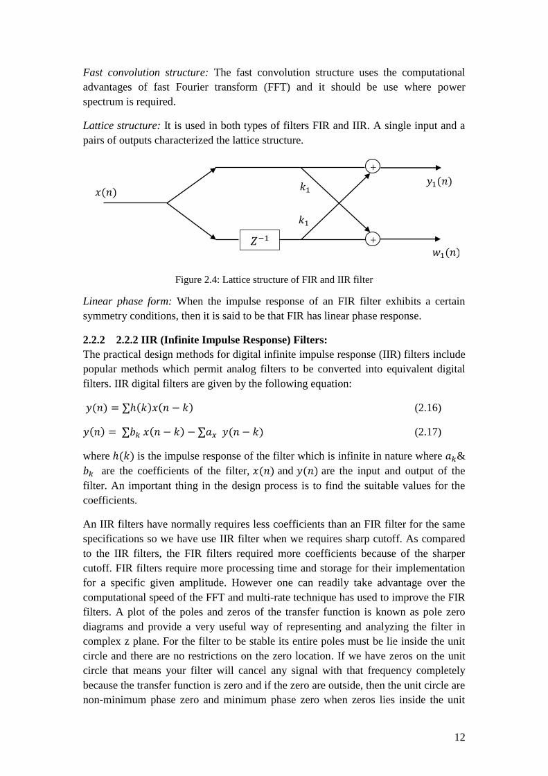
Lattice structure: It is used in both types of filters FIR and IIR. A single input and a
pairs of outputs characterized the lattice structure.
Figure 2.4: Lattice structure of FIR and IIR filter
Linear phase form: When the impulse response of an FIR filter exhibits a certain
symmetry conditions, then it is said to be that FIR has linear phase response.
2.2.2 2.2.2 IIR (Infinite Impulse Response) Filters:
The practical design methods for digital infinite impulse response (IIR) filters include
popular methods which permit analog filters to be converted into equivalent digital
filters. IIR digital filters are given by the following equation:
𝑦(𝑛) = ∑ℎ(𝑘)𝑥(𝑛 − 𝑘) (2.16)
𝑦(𝑛) = ∑𝑏𝑘 𝑥(𝑛 − 𝑘) − ∑𝑎𝑥 𝑦(𝑛 − 𝑘) (2.17)
where ℎ(𝑘) is the impulse response of the filter which is infinite in nature where 𝑎𝑘&
𝑏𝑘 are the coefficients of the filter, 𝑥(𝑛) and 𝑦(𝑛) are the input and output of the
filter. An important thing in the design process is to find the suitable values for the
coefficients.
An IIR filters have normally requires less coefficients than an FIR filter for the same
specifications so we have use IIR filter when we requires sharp cutoff. As compared
to the IIR filters, the FIR filters required more coefficients because of the sharper
cutoff. FIR filters require more processing time and storage for their implementation
for a specific given amplitude. However one can readily take advantage over the
computational speed of the FFT and multi-rate technique has used to improve the FIR
filters. A plot of the poles and zeros of the transfer function is known as pole zero
diagrams and provide a very useful way of representing and analyzing the filter in
complex z plane. For the filter to be stable its entire poles must be lie inside the unit
circle and there are no restrictions on the zero location. If we have zeros on the unit
circle that means your filter will cancel any signal with that frequency completely
because the transfer function is zero and if the zero are outside, then the unit circle are
non-minimum phase zero and minimum phase zero when zeros lies inside the unit
𝑍−1 + +
+ +
𝑤1(𝑛)
𝑦1(𝑛)
𝑘1
𝑘1 𝑥(𝑛)

13
circle. The system, which does not have, zeros in the right half s-plane, are called
minimum phase systems. If a transfer function has poles and/or zeros in right half of
s-plane then it is called non-minimum phase. The phase response is always larger than
for systems, which have minimum phase behavior with same amplitude response.
Many applications such as microwave, radar and optical communications, video
signal processing and digital image processing often used digital filters in order to
manage the constant group delays to overcome the large signal delays, distortion and
disturbances. Infinite impulse response digital filters are mostly preferred against
finite impulse response filters because of their computational performance, frequency
selectivity, and low group delays [6].
But along with this, the designing of IIR filters is much challenging task than FIR
filters since their group delays are non-uniform, and optimization problems becomes
non-convex in result. Transformation of the non-convex IIR filter design had been
achieved by using the Semi-definite programming (SDP), linear programming (LP)
and quadratic programming (QP) which shows better efficiencies by approaching
optimal solution in mini-max and least-squares and least error norm sense.
Design of IIR Filters
The design of IIR filters can be consist of five main stages
Filter specification at which stage the designer gives the function of the filter
and desired performance.
Approximation or coefficient calculations where we select the methods and
calculate the values of coefficient in the transfer function 𝐻(𝑍).
𝐻(𝑍) =𝑌(𝑍)
𝑋(𝑍) (2.18)
Realization, which is simply converting the transfer, functions into a suitable
filter structure. The structure for IIR filters is parallel and cascaded of second
and first filter section.
Analysis of errors that would arise from representing filter coefficient and
carrying out the arithmetic operations involved in filtering with only a finite
number of bits.
Implementation that involves building the hardware or writing the software
codes and carrying out the actual filtering operation [6].
Performance Specification:
The design of the digital IIR filters starts with the specifications of the
performance requirements. These should include:
Characteristics of a signal source or sink.
The frequency response of the filter (the desired amplitude and phase
response and their tolerance.

14
The method of implementation such as a high-level language routine in a
computer or as in a DSP processor based system, choice of a signal
processor and modes of a filtering in real time.
Other design limits such as cost and permissible signal degradation of the
filter.
In general most of the above requirements are application dependent the
designer may not have enough information to specify the filter completely at
the start but as many as the filter requirements as possible should be specified
to simplify the design process.
For frequency selective filters such as low pass and band pass filters the
frequency response specifications are often in the form of tolerance scheme
The following parameters are normally used to specify the frequency response
ℇ2= Passband ripple parameter
𝛿𝑝= Passband deviation
𝛿𝑠= Stopband deviation
The band-edge frequencies are occasionally given in a normalized form that is
a fraction of the sampling frequencies but we have specified them in standard
units of hertz or kilohertz. Pass-band and stop-band deviations may be
expressed as ordinary number or in decibels the pass-band ripples in decibels
is
𝐴𝑝 = 10 log 10 (1 + ℇ2) = −20 log 10 (1 − 𝛿𝑝) (2.19)
And the stop-band attenuation in decibels is
𝐴𝑠 = −20 log 10 (𝛿𝑠) (2.20)
Hence the pass-band ripple is the difference between the minimum and
maximum deviation in the pass-band [5].
Coefficient calculation methods for IIR filters:
There are several ways to design the filters but the most efficient way is that first
designed the analog filter because analog filters can be transform into equivalent IIR
digital filters with similar specifications and then convert the require filter into digital
filter. Following are the different methods to convert analog IIR filters into digital IIR
filters:
Pole Zero Placement Technique
Many applications of the of signal processing contain improve or attenuate
some part of the signal’s frequency spectrum as leaving the remainder of the

15
spectrum unaffected. This effect obtained by using band pass or band stop
filters have frequency response, which considered by gain increasing or
decreasing center frequency𝑓𝑐.
An IIR filter can be calculated by using the formula which combines the
inputs x[n] and outputs y[n] as given below.
𝑦[𝑛] = ∑ 𝑏𝑘𝑀𝑘=0 𝑥[𝑛 − 𝑘] + ∑ 𝑎𝑘
𝑀𝑘=1 𝑦[𝑛 − 𝑘] (2.21)
where the coefficient 𝑏𝑘 is feed forward coefficient as which is only act on the
input signal x[n] as well as 𝑎𝑘 is the feedback coefficient which act on the
output signal y[n]. In Z-transform we know that the input and out relationship
which is
𝑌(𝑧) = 𝐻(𝑧)𝑋(𝑧) (2.22)
The transfer function of the IIR filter is given as:
𝐻(𝑧) =𝑏0+𝑏1 𝑧−1+⋯+𝑏𝑀 𝑧−𝑀
1−𝑎1 𝑧−1−⋯−𝑎𝑁 𝑧−𝑁 (2.23)
Note that the numerator and denominator both are polynomials as all the
polynomials have roots. The roots of the numerator are called “Zeros” of the
filters and the roots of the denominators are called “poles” of the filters [7].
Impulse invariant method
Impulse invariant method is used to find coefficients of IIR filter, first of all
we have to determine analog filter response 𝑯(𝒔) satisfying the specification
then we have to use partial fraction for the expansion of 𝑯(𝒔), obtain the z-
transform of each partial fraction 𝒛 and 𝑯(𝒛) by combining z-transforms of
partial fraction. The main advantages of impulse invariant method is that we
should preserve the stability and order of the analog filter and its disadvantage
is that it is not preferable for high pass and band stop filters and have
distortion in the shape of frequency response due to aliasing [5].
Consider an analog filter
𝐻(𝑠) =𝐶
𝑠−𝛼 (2.24)
The impulse response of the filter is given by
ℎ(𝑡) = 𝐶𝑒𝛼𝑡 (2.25)
Sampled impulse response
ℎ(𝑛) = 𝐶𝑒𝛼𝑛𝑇 (2.26)
Now compute the z-transform

16
𝐻(𝑧) =𝐶
1−𝑒𝛼𝑇𝑧−1 (2.27)
The location of the poles of the filter
𝛼 ⟶ 𝑒𝛼𝑇 (2.28)
In general form
𝛼𝑘 ⟶ 𝑒𝛼𝑘𝑇 (2.29)
The numerator degree should be less than any denominator degree in any
rational transfer function
𝐻(𝑠) = ∑𝐶
𝑠−𝛼𝑘 (2.30)
Similarly
𝐻(𝑧) = ∑𝐶
1−𝑒𝛼𝑘𝑇𝑧−1 (2.31)
The impulse response of the discrete filter ℎ(𝑛𝑇) is same as that of the
analog filter ℎ(𝑡) at the discrete time instants 𝑡 = 𝑛𝑇, 𝑛 = 0, 1, . . .. it is
for this reason that the method is called impulse invariant method.
The sampling frequency affects the frequency response of the impulse
invariant discrete filter. A suitably high sampling frequency is necessary
for the frequency response to be close to that of the equivalent analog
filter.
As is the case of sampled data systems, the spectrum of the impulse
invariant filter equivalent to 𝐻(𝑧) would be the same as that of the original
analog filter, 𝐻(𝑠) but repeats at multiples of the sampling frequency
leading to aliasing. However, if the roll-off of the original analog filter is
sufficiently sharp or if the analog filter is band limited before the impulse
invariant method is applied, the aliasing will be low. Low aliasing can also
be achieved by making the sampling frequency high [5].
Matched Z-transform method
The Matched Z-transform method directly plots the poles and zeros of an
analog filter directly into poles and zeros of the z-plane. This method looks to
work well for some types of analog filters but not in others but it was soon
discovered that improved results could be obtained by adding number of zeros
at the Nyquist point. Matched z-transform method simply to apply as well as
design can be calculated by using calculator and works moderately well not
for low pass and band pass but also for high pass and band stop filters
including elliptic filters. The disadvantages of this method are that the pass
band loss characteristic of digital filter is seriously distorted relative to that of
the analog filter. The high sampling frequency is necessary to obtain good
results, which can introduce certain problems. Z-transform method is very

17
simple that is used to convert analog filter to digital filter by using following
equation:
𝐻(𝑠) = ∑ (𝑠−𝑧𝑘)𝑀
𝑘=1
∑ (𝑠−𝑝𝑘)𝑀𝑘=1
⟶ 𝐻(𝑧) =∑ (1−𝑒𝑧𝑘𝑇𝑧−1)𝑀
𝑘=1
∑ (1−𝑒𝑝𝑘𝑇𝑧−1)𝑁𝑘=1
(2.32)
Poles and zeros are transformed with equation
𝑧𝑘 ⟶ 𝑒𝑧𝑘𝑇 , 𝑝𝑘 ⟶ 𝑒𝑝𝑘𝑇 (2.33)
where T is the sampling time, poles are the same as in impulse invariance
method and zeros should be at new position but this method suffers aliasing
[10].
Bilinear Z- transformation method
The bilinear Z-transformation is important method to obtain IIR filter
coefficients. In this method the main operation required to convert an analog
filter, 𝑯(𝒔) into an equivalent digital filter. The bilinear transform generate a
digital filter whose frequency response has the same characteristics as well as
the frequency response of the analog filter but its phase response may be quite
different. In case of bilinear z-transformation the following equation can be
used for analog to digital conversion.
𝑠 =2
𝑡0
1−𝑧−1
1+𝑧−1 (2.34)
The ratio (𝑧−1)
(𝑧+1) should be used when we want to convert our transfer function
into digital filter and the factor 2
𝑡𝑜 is an optional scaling and it should be cancel
without affecting the final result [5][9].
With the impulse invariant method, after digitizing the analog filter, the impulse
response of the original analog filter is well-maintained but not its magnitude-
frequency response. Because of inherent aliasing the method is unsuitable for high
pass or band stop filters. The bilinear z-transform method on the other hand produces
very efficient filters and is well suited for calculating the coefficients of frequency
selective filters. The impulse invariant method is good for simulating analog systems
with low-pass characteristics, but the bilinear method is best for frequency selective
IIR filters. The matched z-transform shares most of the inherent problems of the
impulse invariant method.
Structure of IIR Filters:
IIR filters consist of three types of structures.
Direct form: This form represents transfer function 𝐻(𝑧) of a filter in a simpler way.
The transfer function 𝐻(𝑧) of 𝑁𝑡ℎ order IIR filter is characterized by 2𝑁 + 1
coefficients. A direct form structure of IIR filter is defined as if the coefficients of

18
multipliers are the coefficients of transfer function. Consider the transfer function
𝐻(𝑧) of first order IIR filter in equation 2.35.
𝐻(𝑧) = 𝑃(𝑧)
𝐷(𝑧)=
𝑝0+𝑝1𝑧−1
1+𝑑1𝑧−1 (2.35)
Consider fourth order IIR filter in figure 2.4
𝐻(𝑧) =∑ 𝑏𝑘𝑧−𝑘4
𝑘=0
1+∑ 𝑎𝑘𝑧−𝑘4𝑘=0
(2.36)
𝑦(𝑛) = ∑ 𝑏𝑘𝑥(𝑛 − 𝑘) − ∑ 𝑎𝑘𝑦(𝑛 − 𝑘)4𝑘=1
4𝑘=4 (2.37)
Figure 2.5: Direct form of IIR filter
Cascade form: A digital filter is realized to be cascade when the numerator and
denominator polynomial of the transfer function 𝐻(𝑧) is a product of polynomials of
a lower degree. Consider a transfer function in equation 2.38
𝐻(𝑧) = 𝑃(𝑧)
𝐷(𝑧)=
𝑃1(𝑧)𝑃2(𝑧)𝑃3(𝑧)
𝐷1(𝑧)𝐷2(𝑧)𝐷3(𝑧) (2.38)
Now, consider an example for cascaded form of IIR filter in figure 2.5
𝐻(𝑧) = 𝐶 ∏1+𝑏1𝑘𝑧−1+𝑏2𝑘𝑧−2
1+𝑎1𝑘𝑧−1+𝑎2𝑘𝑧−22𝑘=1 (2.39)
𝑤1(𝑛) = 𝐶𝑥(𝑛) − 𝑎11𝑤1(𝑛 − 1) − 𝑎21𝑤1(𝑛 − 2) (2.40)
𝑦1(𝑛) = 𝑏01𝑤1(𝑛) + 𝑏11𝑤1(𝑛 − 1) + 𝑏21𝑤1(𝑛 − 2) (2.41)
𝑤2(𝑛) = 𝑦1(𝑛) − 𝑎12𝑤2(𝑛 − 1) − 𝑎22𝑤2(𝑛 − 2) (2.42)
𝑦(𝑛) = 𝑏02𝑤2(𝑛) + 𝑏12𝑤2(𝑛 − 1) − 𝑏22𝑤2(𝑛 − 2) (2.43)
𝑍−1
𝑦(𝑛) 𝑏0 𝑥(𝑛)
𝑍−1
𝑍−1
𝑍−1
+ +
+ +
+ +
+ +
𝑍−1
𝑍−1
𝑍−1
𝑍−1
+ +
+ +
+ +
+ + 𝑏1
𝑏3
𝑏2
𝑏4
−𝑎1
−𝑎2
−𝑎3
−𝑎4

19
Figure 2.6: Cascaded form of IIR filter
Parallel form: In parallel form the transfer function 𝐺(𝑧) have expanded by using
partial fractions. A partial-fraction expansion of the transfer function 𝐺(𝑧) is given by
the following equation 2.44.
𝐺(𝑧) = ∑ƿ𝜄
1−𝜆𝜄𝑧−1𝑁𝑙=1 (2.44)
where ƿ𝜾 is a constant and is called residue is given by equation 2.45.
ƿ𝜾 = (1 − 𝝀𝜾𝑧−1)𝐺(𝑧) (2.45)
Representation of parallel form in figure 2.6
𝐻(𝑧) = 𝐶 + ∑𝑏1𝑘+𝑏1𝑘𝑧−1
1+𝑎1𝑘𝑧−1+𝑎2𝑘𝑧−22𝑘=1 (2.46)
𝑤1(𝑛) = 𝑥(𝑛) − 𝑎11𝑤2(𝑛 − 1) − 𝑎22𝑤2(𝑛 − 2) (2.47)
𝑤2(𝑛) = 𝑥(𝑛) − 𝑎12𝑤2(𝑛 − 1) − 𝑎22𝑤2(𝑛 − 2) (2.48)
𝑦1(𝑛) = 𝑏01𝑤1(𝑛) + 𝑏11𝑤1(𝑛 − 1) (2.49)
𝑦2(𝑛) = 𝑏02𝑤2(𝑛) + 𝑏12𝑤2(𝑛 − 2) (2.50)
𝑦3(𝑛) = 𝐶𝑥(𝑛) (2.51)
𝑦(𝑛) = 𝑦1(𝑛) + 𝑦2(𝑛) + 𝑦3(𝑛) (2.52)
𝑤1(𝑛)
+ + + +
+ +
𝑍−1
𝑍−1
+ +
+ + + +
+ +
𝑍−1
𝑍−1
+ +
−𝑎11
−𝑎21
𝑏11
𝑏21
−𝑎12
−𝑎22
𝑏12
𝑏22
𝑏02 𝑏01
𝑤2(𝑛) 𝑦1(𝑛) 𝑦(𝑛) 𝑥(𝑛)

20
Figure 2.7: Parallel form of IIR filter
Nyquist effect:
The three methods for converting analog filters into equivalent discrete-time filters
are the matched z-transform, the impulse invariant and the bilinear z-transform
methods and have a significant effect on the filter characteristics (e.g. magnitude
phase and group delay responses), in certain cases. The frequency band for analog
filters spreads from zero to infinity, whereas for digital filters it is from zero to the
Nyquist frequency (i.e. half the sampling frequency).
Thus the magnitude-frequency response of digital filters designed using either of three
methods may be significantly different from those of the analog filter because the
entire analog frequency band (zero to infinity) is now compressed into a narrow band
(zero to Nyquist frequency). This difference represents a distortion, which is stated as
Nyquist effect.
In many applications, the Nyquist effect is not harmful besides the provision of
greater attenuation than specified. However, in applications where it is desirable to
hold the analog filter response, such as in professional and semi-professional audio
work, the effect represents an undesirable distortion. In such applications, the extent
+ +
𝑍−1
𝑍−1
+ +
+ + + + 𝑏01
𝑏11 −𝑎11
−𝑎21
𝑤1(𝑛)
𝑍−1
𝑍−1
+ +
+ + + + 𝑏02
𝑏12 −𝑎12
−𝑎22
𝑤2(𝑛)
𝑦1(𝑛)
𝑦2(𝑛)
𝑦3(𝑛)
𝑦(𝑛)
𝑥(𝑛)
𝐶

21
of the distortion would be a factor in the choice of a transform for converting an
analog filter into an equivalent discrete-time filter. The influence on other filter
characteristics, such as group delay and impulse responses, may also be a factor in the
choice of a method [5].
Finite Word Length Affects in IIR filters:
The coefficients, 𝑎𝑘 and 𝑏𝑘 obtained earlier are of infinite or very high precision,
typically six to seven decimal places. When an IIR digital filter is implemented in a
small system, such as an 8-bit microcomputer, errors arise in representing the filter
coefficients and in performing the arithmetic operations specified by the difference
equation. These errors reduce the performance of the filter and filter should be
unstable. Before the implementation of an IIR filter, it is important to determine the
amount to which its performance will be reduced by finite word length effects and to
find a remedy if the reduction is not suitable. In general, the effects of these errors can
be reduced to acceptable levels by using more bits but this may be at the expense of
increased cost.
The main errors in digital IIR filters are as follows:
ADC quantization noise which results from presenting the samples of the input
data, 𝑥(𝑛), by only a small number of bits.
Coefficient quantization errors caused by presenting the IIR filter coefficients by a
finite number of bits.
Overflow errors which result from the additions or accumulation of partial results
in a limited register length.
Product round off errors caused when the output 𝑦(𝑛), and results of internal
arithmetic operations are rounded to the allowed word length
The extent of filter degradation depends on:
(i) The word length and type of arithmetic operations used to perform the
filtering operation.
(ii) The method used to quantize the filter coefficients and variables.
(iii) The filter structure.
From knowledge of these factors, the designer can calculate the effects of finite word
length on the filter performance and take corrective action if necessary. Depending on
how the filter should be implemented some of the effects may be irrelevant. For
example, when implemented as a high-level language program on most large
computers, coefficient quantization and round off errors are not important. For real-
time processing, finite word lengths (typically 8 bits, 12 bits, and 16 bits) are used to
represent the input and output signals, filter coefficients and the results of arithmetic
operations. In these cases, it is always necessary to study the effects of quantization
on the filter performance. The effects of finite word length on performance are more
difficult to analyze in IIR filters than in FIR filters because of their feedback arrange
[5].

22
Quantization Errors Effects on Coefficients:
The primary effect of quantizing filter coefficients using a finite number of bits is to
change the positions of the poles and zeros of 𝐻(𝑧) in the z-plane. This could lead to:
Instability or potential instability for high-order filters, with sharp transition
widths and poles close to the unit circle.
A change in the desired frequency response, the quantized filter should he
analyzed to confirm that its word length is sufficient for both stability and
satisfactory frequency response.
Computational Requirements:
The designer must analyze the impact of the computational requirements of a digital
filter on the processor that will be used. The primary requirements for digital fillers
are multiplication, additions, accumulation and delays or shifts. For example, a filter
consisting of a second-order section would require typically four multiplications, four
additions, and some shifts and storage. If the filtering is performed in real time, for
example at 44.1 kHz (or digital audio) the arithmetic operations must be performed
once every 1 / (44.1 kHz). Allowance must also be made for other overheads such as
fetching the input data or saving or outputting the filtered data samples as well as
other housekeeping operations [5].
2.2.3 Comparison between FIR and IIR Filters
The choice between FIR and IIR mainly depends on their comparisons:
Linear phase response:
FIR filters have linear phase response because there is not any phase distortion in the
signal generated from a filter and this is very important in many signal-processing
applications like data transmission, biomedical, digital audio and image processing.
As compared to FIR filter the IIR filter have non-linear phase response especially at
band edges.
Stability:
As compared to the IIR filters, FIR filters have always-stable response.
Round off noise:
The limited number of bits used to implements the filter such as round off noise and
quantization of coefficients errors is much less in FIR than in IIR.
Coefficient requirement:
As compared to the IIR filters, the FIR filters required have more coefficients because
of the sharper cutoff. FIR filters require more processing time and storage for their
implementation for a specific given amplitude. However one can readily take
advantage over the computational speed of the FFT and multi-rate techniques have
been used to improve the FIR filters.

23
Analog filter transformation:
We can transform analog filters into IIR digital filters with the similar specifications
but it is not possible in the case of FIR filter as they have no analog counterpart.
Easy synthesis:
The arbitrary frequency of the FIR filter should be easy to synthesize.

24
Re-Structured
Re-
Des
igned
Respecify
Re-calculate
3 Design and Implementation of Filters (MATLAB) Designing of filters involves following five basic steps as described earlier in section
2.1.2. Figure 3.1 shows the flow chart of the design stages for digital filters.
Filter Specification
Calculation of Filter Coefficient
Realization of Structure
Analysis of finite word length effects
Implementation
Figure 3.1 Summary of Design Stages for Digital filters (FIR & IIR)
3.1 FIR Filter
Filter specification involves following four parameters:
Pass band attenuation
Stop band attenuation
Pass band edge frequency
Stop band edge frequency
Considering electrical power systems we choose pass-band frequency of 50 Hz,
which is basically used as a standard for power systems [8]. Similarly the harmonic
START
Filter Specification
Finite word length
effects analysis &
Solution
Calculations for Filter
Coefficients
Structure Realization
STOP
Hardware/Software
Implementation &
Testing

25
components are the multiples of pass-band frequency so the first harmonics will have
frequency of 100 Hz therefore the stop-band edge frequency is selected as 90 Hz.
Now stop band attenuation should be as large as possible and pass band attenuation
should be as small as possible in order to have more precise and accurate
measurements. The sampling frequency was chosen to be 300 Hz and pass-band and
stop band frequencies must be converted in radians as the signal processing toolbox
operates with normalized frequencies in filter design functions. To convert these pass
band and stop band frequencies to normalized frequencies we will divide them by one
half of the sampling frequencies. Similarly these normalized frequencies are
multiplied by π to get angular frequency around the unit circle. We have calculated 40
dB and 1 dB stop band and pass band attenuation respectively from equations 2.19
and 2.20.
Ωp = 50𝐻𝑧
150𝐻𝑧= 0.33*π = Pass band edge frequency in Radians
Ωs = 90𝐻𝑧
150𝐻𝑧= 0.6*π = Stop band edge frequency in Radians
As = 40 dB = Stop band attenuation
Rp = 1 dB = Pass band ripples or attenuation
Fs = 300 samples/sec
Since the equation the FIR filter is given by
𝑦(𝑛) = ∑ℎ(𝑘)𝑥(𝑛 − 𝑘) 0 ≤ 𝑘 ≤ 𝑁 − 1 (3.1)
Now the next step is to calculate the filter coefficient ℎ(𝑛) so filter meets the design
specifications. Several methods are used to calculate the filter coefficients as
discussed in chapter 2, but we chose window method which is easy to calculate and
implement without using any software as in case of optimal method.
The basic idea behind the window method is to choose proper ideal filter, which has a
non-casual, infinite duration impulse response, and then truncate its impulse response
to obtain the linear phase and casual FIR filter. In the window methods we actually
multiply the ideal response by a window function to obtain the finite impulse
response.
Now among different window function we select Kaiser window function for this
application because its provides maximum stop band attenuation as compared to other
window functions and also has a ripple control parameter and it is also more efficient
in terms of the number of coefficients to meet the same specifications. Kaiser window
is one of the useful and optimum window, optimum in sense of providing large main
lobe width for the given stop-band attenuation which gives the sharpest transition
width and it also provide flexible transition bandwidth.

26
We implemented the Kaiser Window function 𝑤(𝑛) in MATLAB, and then obtained
the impulse response ℎ(𝑛) of our filter by multiplying the window function by the
ideal response ℎ𝑑(𝑛) of the low pass filter. This is given by the simple equation
ℎ(𝑛) = ℎ𝑑(𝑛) ∗ 𝑤(𝑛) (3.2)
Figure 3.2 shows the impulse response before and after windowing. The impulse
response becomes finite after windowing that why it is called finite impulse response
filter.
Figure 3.2: Plot of coefficients obtained or impulse response h(n)
Coefficients of ℎ(𝑛) at M=19
0.0029, -0.0077, -0.0121, 0.0162, 0.0340, -0.0253, -0.0854, 0.0323, 0.3109, 0.4650,
0.3109, 0.0323, -0.0854, -0.0253, 0.0340, 0.0162, -0.0121, -0.0077, 0.0029
The filter function 𝐻(𝑧) is obtained by taking the Fourier transform of the impulse
response is given by
𝐻(𝑧) = ∑ℎ(𝑛)𝑧 − 𝑛 0 ≤ 𝑛 ≤ 𝑁 − 1 (3.3)
The filter function thus obtained was plotted to check the filter performance and is
shown in the figure 3.3.
0 2 4 6 8 10 12 14 16 18-0.2
0
0.2
0.4
0.6
n
Hd
ideal response
0 2 4 6 8 10 12 14 16 18-0.2
0
0.2
0.4
0.6
n
n
windowed response

27
Figure 3.3: Frequency response of low pass FIR filter
From the figure 3.3 we obtained the results as given in specifications, that is cut off
frequency 0.33π and stop band is 0.6π radians.
Figure 3.4: Phase reponse of low pass FIR filter
From the figure 3.4 we see that the phase response of our designed filter is linear and
so it is prove that FIR filters have a linear phase response.
3.2 IIR Filter
IIR low pass filter specification involves the same four steps as of FIR low pass filter.
So here we have selected the same specification of IIR low pass filter as selected in
previous section for FIR low pass filters that are:
0 0.1 0.2 0.3 0.4 0.5 0.6 0.7 0.8 0.9 10
0.5
1
freq in pi units
magnitude o
f H
amplitude spectrum
0 0.1 0.2 0.3 0.4 0.5 0.6 0.7 0.8 0.9 1-100
-50
0
freq in pi units
mag o
f H
(dB
)
amplitude spectrum
0 0.1 0.2 0.3 0.4 0.5 0.6 0.7 0.8 0.9 1-1
-0.5
0
0.5
1
freq in pi units
radia
ns
filtered signal phase spectrum

28
Ωp = 0.33*π = Pass band edge frequency in Radians
Ωs = 0.6*π = Stop band edge frequency in Radians
As = 40 dB = Stop band attenuation
Rp = 1 dB = Pass band ripples or attenuation
Fs = 300 samples/sec
Since IIR filter is characterized by the following equation
𝑦(𝑛) = ∑ℎ(𝑘)𝑥(𝑛 − 𝑘) 0 ≤ 𝑘 ≤ ∞ (3.4)
𝑦(𝑛) = ∑𝑏𝑘𝑥(𝑛 − 𝑘) − ∑𝑎𝑘𝑦(𝑛 − 𝑘) 0 ≤ 𝑘 ≤ 𝑁, 1 ≤ 𝑘 ≤ 𝑀 (3.5)
Next step is to calculate the filter coefficients 𝑎𝑘 & 𝑏𝑘
For coefficient calculations we have choose impulse invariant method is best suited
for the low filtering because the impulse response of the original analog filter is
preserved. In this method starting with suitable analog transfer function 𝐻(𝑠), the
impulse response ℎ(𝑡) is obtained using Laplace transform. The ℎ(𝑡) thus obtained is
suitably sampled to produce ℎ(𝑛𝑇), and the desired transfer function 𝐻(𝑧) is thus
obtained by z-transforming ℎ(𝑛𝑇) where T is the sampling interval. Impulse invariant
method has been used to calculate the coefficient where 𝑎𝑘 & 𝑏𝑘 after calculating the
coefficients the frequency response was plotted in MATLAB to check whether the
design meets the requirements.
Coefficients at M=9
b= 0.0000, 0.0000, 0.0036, 0.0284, 0.0491, 0.0242, 0.0034, 0.0001, 0.0000
a= 1.0000, -3.0110, 4.8837, -5.1117, 3.7117, -1.9067, 0.6856, -0.1651, 0.0240, -
0.0016

29
Figure 3.5: Frequency reponse of low pass IIR filter
From the figure 3.5 we see that we have desired results as given in specifications, that
is cut off frequency is 0.33π and stop band is 0.6π Radians.
Figure 3.6: Phase response of IIR low pass filter
From figure 3.6 we see that the phase responses of IIR low pass filter. It is seen that
the phase response is non-linear thus proving the fact that IIR filters are non-linear in
nature.
0 0.1 0.2 0.3 0.4 0.5 0.6 0.7 0.8 0.9
-70
-60
-50
-40
-30
-20
-10
0
Normalized Frequency ( rad/sample)
Magnitu
de (
dB
)
Magnitude Response (dB)
0 0.1 0.2 0.3 0.4 0.5 0.6 0.7 0.8 0.9 1-4
-2
0
2
4
radia
ns
freq in pi units
phase response

30
4 Structure Design for Field Programmable Gate Array
(FPGA) through Digital Filters
4.1 Introduction:
A FPGA (Field programmable gate array) is a semiconductor device, which is used to
process digital information by utilizing gate array technology and should be re-
programmed after it is manufactured. A FPGA consists of programmable logic
components called logic blocks and programmable interconnects. We can
programmed logic blocks to perform the functions of basic logic gates such as AND,
and XOR, or simple mathematical functions or complex combinational functions such
as decoders. In most FPGAs the logic blocks also consist of memory elements, which
may be, flip flops or more complete blocks of memories.
In the previous years, for the purpose of designing in VLSI areas FPGA (Field
Programmable Gate Arrays) increased importance. Now a day FPGAs offer a large
number of applications such as equivalent gates, which can be clocked at high
frequencies. Moreover, because of the re-configurability, FPGA provide the fastest
approach to system prototype and reliable instruments to match in hardware but the
performance of systems are too much complicated to be simulating in software. For
these reasons, it can make sense to extract information on a system by its
implementation on FPGAs followed by measurements on the hardware, instead of
simulations [9].
4.2 FPGA Structure:
Xilinx is the biggest manufacturer of FPGA and the Xilinx FPGA consist of three
blocks:
CLB: It is the configurable logic block of FPGA, which is used to calculate
the specific functions defined by the users. The CLBs should be found on the
center of the chip. It is used for the implementation of combinational and
sequential logic, for this purpose CLBs consist of lookup table (LUT) which
can be controlled by 4-inputs for the implementation of combinational logics
and used D-flip flops for sequential logics. MUX should be used to select
between the output of combinational and sequential logics. We can program
CLBs by using the truth table of LUT and control bit of MUX (multiplexer)
and these both structures are useful for the implementation of combinational
and sequential logics.
IOB: The input/output block of the FPGA used to connect it to the other
elements of the applications and IOBs are located on the periphery.
Interconnect: This part is used for the writing between CLB and between IOBs
and CLBs and interconnects are used to implement different programs on the
FPGA. IOBs are used to get signals in the and out of the FPGA, means it
should be used as input and output [10].

31
4.2.1 Modern FPGAs
In modern FPGA we have additional information units, which are easier and efficient
for the designing of applications, as well as arithmetic units and small memories are
very difficult to implement on CLB (configurable logic block). Therefore in modern
FPGAs embedded memories and embedded logic blocks are used for arithmetic
operations and the most common is multiplications. With the use of embedded blocks
in FPGA we get more memory and speed therefore embedded memories are easy to
interface than external memories. DSP applications are very useful in the
implementation of FPGA like multipliers are the function on FPGA for the
implementation of DSP applications. Furthermore embedded processor cores are also
the part of FPGA for the purpose of better communication between microprocessor
and FPGA and the main advantages of embedded processor is that it reduces the
latency of communication between FPGA and microprocessor. In comparison with
the embedded processors the soft cores should be directly the part of FPGA fabric as
soft cores are easy to configurable and have the same clock as that of FPGA, and its
main advantage is that it is easy to interface and drawback is that they have slower
clock rate [11].
4.2.2 Configuring FPGA
FPGAs should not be programmed directly so synthesis tools are used to program
FPGAs, which are used to translate code into bit stream, and downloaded to FPGAs;
commonly hardware description language is used to configure the devices.
Furthermore high-level languages and library-based solutions are also possible to use
for the configuration of the FPGAs.
Hardware description language is the most common language used for the
programming of FPGAs, there are also two other languages like VHDL and Verilog
both languages are internationally recognized and are powerful. VHDL was
developed in 1980 and is the extension of ADA and should be used for describing the
hardware and Verilog is like C programming language to design hardware and have
recognized internationally like VHDL. To configure FPGA with HDL a developer
require two programs, one tool which is used to test and simulate the configurations
on pc and a synthesis tool which is used to convert code into bit stream and
downloaded into the FPGA.
High-level languages are also used for the designing and implementation of FPGA
applications more like software development. SystemC is a C++ library, which is
used to implement and simulate the processing of hardware in C++ syntax. By using
Accel-chip it is easy to implement VHDL and Verilog code block for MATLAB DSP
function.
In library-based solutions to designing FPGAs, the FPGAs developer Xilinx and
Altera provide macros with parameterized solutions, which is used for arithmetic
operations and required less development time [11].

32
4.2.3 Applications of FPGA
FPGAs include digital signal processor, software defined radio, aerospace,
defense system, ASIC prototyping, medical imaging, computer vision, speech
recognition, bioinformatics and computer hardware emulation [12].
FPGAs originally began as competitor to CPLDs and due to their size,
capabilities and speed they began to take over larger and larger function and
are now marketed as full systems on chip (SOC).
FPGAs are increasingly used in conventional high performance computing
applications where computational kernels such as FFT or Convolution are
performed on the FPGA instead of a microprocessor and the use of FPGA for
computing tasks is known as reconfigurable computing.
4.2.4 Advantages of FPGA
FPGA consist of large number of logic blocks which is used for larger
memory, FPGA computers have no given processor structure but they offer a
large amount of logic gates, registers, RAM and routing resources. It is used to
perform large number of logical and arithmetic operations for variable storage
and to transfer data between different parts of the computer. Typically
thousands of operation can be done on FPGA computers during every clock
cycle.
When the applications of FPGA were specific, then specialized tools were
used to access them but by using hard and configurable soft cores, FPGAs are
now controlled to perform in mainstream embedded applications and it means
the accessibility of embedded software and tools becomes a necessity.
FPGA are controlling programmable logic integrated circuits and is use to
design digital logic as you can design your circuit on your computer and run it
on FPGA.
FPGA are quick devices.
4.3 Design of Structures for FPGA:
We will design the structure for both filters that are FIR and IIR, which we will,
further use in FPGAs.
4.3.1 Using FIR Filter:
After calculating the coefficients in section 3.1, we will choose suitable structure for
FIR filter realization and the order of the filter is 𝑀 − 1 where 𝑀 is the number of
coefficients and the length of the filter is equal to 𝑀.
Among different structures like direct form, cascade form, parallel form and linear
phase structure, we have chosen linear phase structure because the impulse response
in our FIR filter is symmetric as shown in figure 3.2 and due to symmetrical response
in the impulse response of linear phase FIR filter to reduce the computational
complexity of the filter implementation, it is more efficient and reduce the number of
additions and multiplications. Linear phase structure is same as direct form but it
should be implemented differently as it reduces the multiplication process to half. The

33
linear phase structure provides no delay distortion but only fixed amount of delay. For
the filter of length 𝑀 − 1 the minimum operations are 𝑀/2 . The linear phase
structure is shown in figure 4.1 by using the coefficients of FIR filter.
Figure 4.1: Linear Phase FIR filter structure
The number of blocks formed in our structure in figure 4.1 can be calculated by using
the formula 𝐾 = 𝑀/2 so in our case𝐾 = 19/2 = 9. This structure also forms a sort
of systolic structure in which input should be pumped in, in the form of continuous
input samples. In the first block the coefficient 𝑏𝑜 is multiplied by 𝑥(𝑛) and the
delayed version of 𝑥(𝑛) coming from the last block that is 𝑥(𝑛 − 𝑀 + 1), where 𝑀 is
the length. Similarly the second coefficient 𝑏1 is multiplied by 𝑥(𝑛 − 1) and the
delayed version of 𝑥(𝑛) coming from the second last block that is 𝑥(𝑛 − 𝑀 + 2). The
multiplication process goes on for the all the coefficients but reduced to half further
all these products are added up to give the accumulated output 𝑦(𝑛).
4.3.2 Using IIR Filter:
Similarly we construct the structure of IIR filter from the coefficients calculated in
section 3.2 for IIR filter. Like FIR filters, the IIR filters can also be realized using
different structure as discussed earlier. We will implement direct form structure for
the realization of our filter in FPGA because direct form structure involves simple
multiplications, additions and delays that is shown in figure 4.2.
On the left hand side in the figure 4.2 we see that the inputs are being delay and
multiplied by each of the coefficients and all the products should be added together
and similarly the right hand side is the mirror image of left hand side. Thus all the
coefficients are multiplied one by one leading to the number of multiplications equal
to the total number of coefficient and then further added all the products to get the
required output 𝑦(𝑛).
𝑦(𝑛)
𝑧−1
𝑧−1
𝑧−1
𝑧−1
𝑧−1 𝑧−1
𝑥(𝑛)
𝑏0
INTERMIDIATE BLOCK LAST BLOCK FIRST BLOCK
𝑏7 𝑏8 𝑏9

34
Figure 4.2: Structure for direct form IIR filter
𝑍−1
𝑍−1
𝑍−1
𝑍−1
𝑍−1
𝑍−1
𝑍−1
𝑍−1
𝑍−1
𝑍−1
𝑍−1
𝑍−1
𝑍−1
𝑍−1
𝑍−1
𝑍−1
𝑍−1
𝑏0
𝑏1
𝑏2
𝑏3
𝑏4
𝑏5
𝑏6
𝑏7
𝑏8
−𝑎1
−𝑎2
−𝑎3
−𝑎4
−𝑎5
−𝑎6
−𝑎7
−𝑎8
−𝑎9
𝑦(𝑛) 𝑥(𝑛)
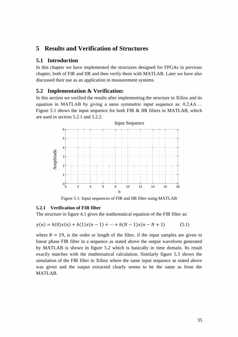
35
5 Results and Verification of Structures
5.1 Introduction
In this chapter we have implemented the structures designed for FPGAs in previous
chapter, both of FIR and IIR and then verify them with MATLAB. Later we have also
discussed their use as an application in measurement systems.
5.2 Implementation & Verification:
In this section we verified the results after implementing the structure in Xilinx and its
equation in MATLAB by giving a same symmetric input sequence as: 0,2,4,6….
Figure 5.1 shows the input sequence for both FIR & IIR filters in MATLAB, which
are used in section 5.2.1 and 5.2.2.
Figure 5.1: Input sequences of FIR and IIR filter using MATLAB
5.2.1 Verification of FIR filter
The structure in figure 4.1 gives the mathematical equation of the FIR filter as:
𝑦(𝑛) = ℎ(0)𝑥(𝑛) + ℎ(1)𝑥(𝑛 − 1) + ⋯ + ℎ(𝑁 − 1)𝑥(𝑛 − 𝑁 + 1) (5.1)
where 𝑁 = 19, is the order or length of the filter, if the input samples are given to
linear phase FIR filter in a sequence as stated above the output waveform generated
by MATLAB is shown in figure 5.2 which is basically in time domain. Its result
exactly matches with the mathematical calculation. Similarly figure 5.3 shows the
simulation of the FIR filter in Xilinx where the same input sequence as stated above
was given and the output extracted clearly seems to be the same as from the
MATLAB.
0 2 4 6 8 10 12 14 16 180
1
2
3
4
5
6
Input Sequence
Am
pli
tude
n

36
Figure 5.2a: Output sequence of pulses of FIR filter
Figure 5.3b: Output sequence of pulses of FIR filter using convolution
Figure 5.4c: Scaled Output sequence of pulses of FIR filter using convolution
Here figure 5.2a shows the FIR filter output using filter function of MATLAB and
figure 5.2b shows the convolved output using convolution function of MATLAB.
Both outputs are same as the convolution results in mirroring the sequence in reverse
0 2 4 6 8 10 12 14 16 18-1
0
1
2
3
4
5
6
Output
y
n

37
order after middle sample. The figure 5.2c shows the scaled output of convolution
between 0 - 255 for improved visibility.
Figure 5.5: Test bench of waveform obtained from verilog simulation for FIR structure
Here xin[35:0] is the 36 bit input of the structure and out[19:0] shows the output at
the given input sequence which is further discussed in section 5.2.3. CLK and rst is
the clock and reset buttons respectively.
5.2.2 Verification of IIR filter
Similarly the structure shown in figure 4.2 is implemented in the Verilog (Xilinx) and
the results obtained from the simulation of the Verilog code on Xilinx are compared
with the MATLAB simulation. The input sequence applied here are same as
mentioned earlier like used for FIR inputs. Figure 5.4 shows the output sequence in
time domain, which matches with the simulation result obtained from the Xilinx that
is figure 5.5.
𝑦(𝑛) = ∑ 𝑏𝑘 𝑥(𝑛 − 𝑘) − ∑ 𝑎𝑘𝑦(𝑛 − 𝑘) 0 ≤ 𝑘 ≤ 𝑁, 1 ≤ 𝑘 ≤ 𝑀 (5.2)
Figure 5.6a: Output sequence of IIR filter using MATLAB
0 2 4 6 8 10 12 14 16 180
1
2
3
4
5
Output
y
n

38
Figure 5.7b: Scaled Output sequence of IIR filter using MATLAB
The IIR filter is implemented using impulse invariance method so figure 5.4a shows
the output sequence of the filter for the given input and figure 5.4b shows the scaled
output of IIR filter between 0 – 255 for improved visibility.
Figure 5.8: Test bench of waveform obtained from verilog simulation for IIR filter
5.2.3 Comparing:
The comparison of our results between MATLAB and FPGA, which clearly shows
that the outputs obtained from the Xilinx are verified with the MATLAB. But FIR
structure gives more accurate than the IIR based structure.
Now if you look at the output sequence of FIR filter obtained from MATLAB results
we get 0,2, 4.3, 5.5, 4.3, 2, 0.4, 2 …and same is the case with the output of the
structure designed in Verilog coding, here as the output is represented in bits form so
they are shown in integer values as one can see from the figure 5.3 that is 0, 2, 4, 6, 4,
2, 1, 2 … which is also symmetric and can be verified from the MATLAB output
sequence of FIR filter.
Similarly for IIR sequence we obtain the sequence 5, 3, 2, 1, 2, 4, 5, 3 … from
designed structure which can be easily verified from the MATLAB output sequence

39
that is 0.5, 1.5, 2.5, 4.3, 4.5, 3, 2, 1 … shown in figure 5.4a. Here if one can see the
output sequence of FIR gives better results, but the performance of both filters is
degraded by finite word length effect, because accuracy is not achieved in this case.
The degradation is more severe in IIR than FIR. This effect can be mitigated by using
more number of bits or by using floating-point arithmetic for coefficients.
5.3 Digital Filters as a part of Measuring System:
Digital filters can be made a part of a power measuring system, which makes use of
digital filtering to separate the fundamentals components from harmonics. Thus active
power and reactive power are measured separately. From the power measurements
one can estimate the efficiency of power distribution unit. As the harmonics generated
by non-linear loads are hazardous for entire power system and are inevitable, there is
an ultimate need to develop a measuring and testing system for the real time loads, as
these are non-linear in nature most of the times.
A typical measuring system consists of following main modules.
Analog-to-Digital conversion
5V to 3.3V conversion
Digital filters and calculations on FPGA
Display
Figure 5.9: Block Diagram of multi-measuring system
The description of all these modules is described below:
5.3.1 Analog-to-Digital conversion
Analog-to-Digital conversion is necessary for the analog data to be processed on
FPGA. Analog-to-Digital conversion is done by chip AD 0808. AD0808 is a
monolithic CMOS (Complementary Metal Oxide Semiconductor) is a data acquisition
component with the resolution of 8-bits conversion, 8-channel multiplexer and a
compatible processor which is used for logic control. By the means of three select
lines we can select any 1 of 8 analog inputs to be converted into digital 8-bits output
at a time. Its main features are that it is easy to interface to all microprocessors; it
Voltage
(V) PRE LPF
PRE LPF
I/V CONV
ADC
IIR HPF
ADC
IIR LPF
IIR LPF
IIR HPF
Multipler
Multipler
Display
Display
Current
(I)
FPGA

40
operates at 5𝑣𝐷𝐶 with adjustable voltage reference, no zero or full scale adjusts
required, 0𝑉 − 𝑉𝑐𝑐 input range, 8-channel multiplexer with logic control and its output
meets TTL (Transistor-Transistor logic) voltage level specifications.
Table 5.1: Specs of Analog to Digital Converter
Its operation time is normally on clock
frequency is 640 kHz and uses
approximation technique for the
conversion and it is available in 28-pin
DIP package (ADC0808CCN). It
provides high speed and accuracy with
minimal temperature dependence for
this it is used in many control and
automatic applications.
Its pin configurations are as follow [13]:
Pins 1, 2, 3,4,5,27,28 are the seven input pins which are not connected.
Pins 6(start) and Pin 7(end of conversion) are short-circuited.
Pin 9(output enable) is at logic 1.
Pin 10 is for clock.
Pin 11(Vcc) & Pin 12(Vref+) are short-circuited and at logic 1.
Pin 13 (GND) & Pin 16(Vref-) are short-circuited and at logic 0.
Pin 22 (ALE) is enabled only when address on the select lines changes
however it is set at logic 1.
Pin 17, 14, 15,8,18,19,20,21 are8-bits of digital output where Pin 17 is LSB
and Pin 21 is MSB.
As 28 = 256 so input signal is quantized in 256 discrete levels where the size of each
level is 0,02V.
5.3.2 The 5V to 3.3V conversion
The output samples of the ADC assumes logic1 at 5V while the logic1 on FPGA
board (SPARTAN 3) is equal to 3.3V, so some additional circuitry is required for the
transformation of voltage levels of ADC samples. Using LM348 chip, which consist
of Quad operational amplifier package, does the additional transformation. The 8-bit
digital output of ADC is fed into two LM348 chips while each individual bit of ADC
is provided to non-inverting input of operational amplifier whose gain is unity. The
supply voltages are given as 3.3V and -3.3V instead of +15V in order to get the
output logic1 of the operational amplifier equal to 3.3V.
The analog input is fed into ADC to convert the analog input into digital current and
voltage samples which are then fed into the FPGA filter after passing through the
regulator of 3.3V, FPGA here also serve the purpose of current and voltage samples
multiplications in order to measure power and output should be displayed.
Resolution 8 bits
Total unadjusted error ±1
2𝐿𝑆𝐵 𝑎𝑛𝑑 ± 1 𝐿𝑆𝐵
Single supply 5𝑉𝐷𝐶
Low power 15mW
Conversion time 100 us

41
Thus our both filters FIR & IIR can be efficiently utilized as a part of our
measurement system to accurately measure active, harmonics and other related
parameters.

42
6 Conclusion
This report concludes with the application of the digitals filters in measuring systems
and shows an expected error threshold level. It gives an advanced maturity and
estimation of quality for implementing high resolution and high quality applications
of digital signal processing. Due to the implemented precision and accuracy, the
presented filters can also be made an integral part of many modern applications,
where ever a high accuracy and finite error is required. The design can also be
implemented in Application Specific Integrated Circuit (ASIC), which will reduce the
overall cost on the filters.

43
7 Appendix A (Code)
A.1 FIR LOW-PASS FILTER (MATLAB, M=19) Clc; Clear all; Close all;
WP=.33*pi; ws=.6*pi; tr_width=ws-wp; As=40; M=ceil((As-7.95)/(14.36*tr_width/(2*pi))+1)+1; M=19; n=[0:1:M-1]; if As>=50 beta=0.1102*(As-8.7); else beta=(.5842*((As-21)^.4))+(.7886*(As-21)); end wc=(ws+wp)/2; alpha=(M-1)/2 m=n-alpha+eps; hd=sin(wc*m)./(pi*m); subplot(2,1,1); stem(n,hd); xlabel('n'); ylabel('Hd'); title('ideal response');grid w_kai=(kaiser(M,beta))'; h=hd.*w_kai; H=freqz(h,1,500); k=0:499; w=(pi/500)*k; subplot(2,1,2); stem(n,h); xlabel('n'); ylabel('n'); title('window response'); grid db=20*log10(abs(H)/max(abs(H))); figure; subplot(2,1,1); plot(w/pi,abs(H)); xlabel('freq in pi units'); ylabel('magnitude of H'); title('amplitude spectrum'); grid subplot(2,1,2); plot(w/pi,db); xlabel('freq in pi units'); ylabel('mag of H(dB)'); title('amplitude spectrum'); grid xin=cos(.2*pi*n)+cos(.4*pi*n)+cos(.6*pi*n); X=xin*(exp(-j*pi/500)).^(n'*k); y=filter(h,1,xin); Y=y*(exp(-j*pi/500)).^(n'*k); figure; subplot(2,1,1); plot(w/pi,abs(X)); xlabel('freq in pi units ');ylabel('|X|');title('input signal
spectrum');

44
grid subplot(2,1,2); plot(w/pi,abs(Y)); xlabel('freq in pi units'); ylabel('|Y|'); title('filtered signal spectrum'); grid db=20*log10(abs(Y)/max(abs(Y))); db1=20*log10(abs(X)/max(abs(X))); figure; subplot(2,1,1);plot(w/pi,db1); xlabel('freq in pi units'); ylabel('|X|(dB)'); title('input signal spectrum'); grid subplot(2,1,2);plot(w/pi,db); xlabel('freq in pi units'); ylabel('|Y|(dB)'); title('filtered signal spectrum');grid figure; subplot(2,1,1); plot(w/pi,angle(H)/pi); xlabel('freq in pi units'); ylabel('radians'); title('filtered signal phase spectrum'); grid
db=20*log10(abs(H)/max(abs(H))); figure; subplot(2,1,1); plot(w/pi,abs(H)); xlabel('freq in pi units'); ylabel('magnitude of H'); title('amplitude spectrum'); grid subplot(2,1,2); plot(w/pi,db); xlabel('freq in pi units'); ylabel('mag of H(dB)'); title('amplitude spectrum');grid xin=cos(.2*pi*n)+cos(.4*pi*n)+cos(.6*pi*n); X=xin*(exp(-j*pi/500)).^(n'*k); y=filter(h,1,xin); Y=y*(exp(-j*pi/500)).^(n'*k); figure; subplot(2,1,1);plot(w/pi,abs(X)); xlabel('freq in pi units'); ylabel('|X|'); title('filtered signal spectrum'); grid db=20*log10(abs(Y)/max(abs(Y))); db1=20*log10(abs(X)/max(abs(X))); subplot(2,1,2); plot(w/pi,db); xlabel('freq in pi units'); ylabel('|Y|(dB)'); title('filtered signal spectrum');grid figure; plot(w/pi,angle(H)/pi); xlabel('freq in pi units'); ylabel('radians');

45
title('filtered signal phase spectrum');grid
A.2 IIR LOW PASS FILTER (MATLAB, M=9) wp=0.33*pi; ws=0.6*pi; Rp=1; As=40; T=1; OmegaP=wp/T;OmegaS=ws/T; [cs,ds]=afd_butt(OmegaP,OmegaS,Rp,As);
[b,a]=imp_invr(cs,ds,T);
function[b,a]=afd_butt(wp,ws,rp,As); if wp<=0 error('passband edge must be larger than zero') end
if wp<=wp error('stopband edge must be larger than passband edge') end
if(rp<=0)|(As<0) error('PB ripple and/or SB attenuation must be larger than zero') end
N=ceil((log10((10^(rp/10)-1)/(10^(As/10)-1)))/(2*log10(wp/ws))) fprintf('\n***Butterworth filter order=%2.0f\n',N) omegac=wp/((10^(rp/10)-1)^(1/(2*N))) [b,a]=u_buttap(N,omegac);
function [b,a]=imp_invr(c,d,T); [R,p,k]=residue(c,d); p=exp(p*T); [b,a]=residuez(R,p,k); b=real(b'); a=real(a');
function [b,a]=u_buttap(N,omegac); [z,p,k]=buttap(N); p=p*omegac; k=k*omegac^N; B=real(poly(z)); b0=k; b=k*B; a=real(poly(p));
A.3 FIR LOW PASS FILTER (VERILOG)
module multiply(a,b,out);
input [35:0] a;
input [35:0] b;
output [35:0] out;
assign out = a*b;
endmodule
module add(a,b,out);
input [35:0] a;
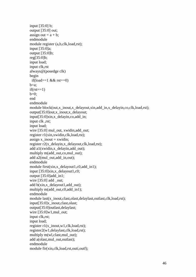
46
input [35:0] b;
output [35:0] out;
assign out = a + b;
endmodule
module register (a,b,clk,load,rst);
input [35:0]a;
output [35:0]b;
reg[35:0]b;
input load;
input clk,rst
always@(posedge clk)
begin
if(load==1 && rst==0)
b=a;
if(rst==1)
b=0;
end
endmodule
module block(out,x_inout,x_delayout,xin,add_in,x_delayin,co,clk,load,rst);
output[35:0]out,x_inout,x_delayout;
input[35:0]xin,x_delayin,co,add_in;
input clk ,rst;
input load;
wire [35:0] mul_out, xwidin,add_out;
register r1(xin,xwidin,clk,load,rst);
assign x_inout = xwidin;
register r2(x_delayin,x_delayout,clk,load,rst);
add a1(xwidin,x_delayin,add_out);
multiply m(add_out,co,mul_out);
add a2(mul_out,add_in,out);
endmodule
module first(xin,x_delayout1,c0,add_in1);
input [35:0]xin,x_delayout1,c0;
output [35:0]add_in1;
wire [35:0] add _out;
add b(xin,x_delayout1,add_out);
multiply m(add_out,c0,add_in1);
endmodule
module last(x_inout,clast,olast,delaylast,outlast,clk,load,rst);
input[35:0]x_inout,clast,olast;
output[35:0]outlast,delaylast;
wire [35:0]w1,mul_out;
input clk,rst;
input load;
register r1(x_inout,w1,clk,load,rst);
register2(w1,delaylast,clk,load,rst);
multiply m(wl,clast,mul_out);
add a(olast,mul_out,outlast);
endmodule
module fir(xin,clk,load,rst,outi,outf);

47
input [35:0] xin;
output [19:0] outi;
output [15:0] outf;
input clk,load,rst;
wire [35:0] c0,c1,c2,c3,c4,c5,c6,c7,c8,c9;
wire [35:0] temp;
assign outi=temp[35:16];
assign outf=temp[15:0];
assign c0= 36'd190;
assign c1= 36'd68719476232;
assign c2= 36'd68719475944;
assign c3= 36'd1061;
assign c4= 36'd2228;
assign c5= 36'd68719475078;
assign c6= 36'd68719471140;
assign c7= 36'd2116;
assign c8= 36'd20480;
assign c9= 36'd30720;
wire[35:0]add_in1,x_delayoutl,x_delayout2,x_delayout3,x_delayout4,x_delayout5,x_
delayout6,x_delayout7,x_delayout8,x_delayout9,delaylast;
wire [35:0]o1,o2,o3,o4,o5,o6,o7,o8,o9;
wire
[35:0]x_inout1,x_inout2,x_inout3,x_inout4,x_inout5,x_inout6,x_inout7,x_inout8;
first fl(xin,x_delayout1,c0,add_in1);
last l1(x_inout8,c9,o8,delaylast,temp,clk,load,rst);
block b1(o1,x_inout1,x_delayoutl,xin,add_in1,x_delayout2,c1,clk,load,rst);
block b2(o2,x_inout2,x_delayout2,x_inout1,01,x_delayout3,c2,clk,load,rst);
block b3(o3,x_inout3,x_delayout3,x_inout2,02,x_delayout4,c3,clk,load,rst);
block b4(o4,x_inout4,x_delayout4,x_inout3,03,x_delayout5,c4,clk,load,rst);
block b5(o5,x_inout5,x_delayout5,x_inout4,04,x_delayout6,c5,clk,load,rst);
block b6(o6,x_inout6,x_delayout6,x_inout5,05,x_delayout7,c6,clk,load,rst);
block b7(o7,x_inout7,x_delayout7,x_inout6,06,x_delayout8,c7,clk,load,rst);
block b8(o8,x_inout8,x_delayout8,x_inout7,07,delaylast,c8,clk,load,rst);
endmodule
A.4 IIR LOW PASS FILTER (VERILOG)
`timescale 1ns/1ps
module multiply(a,b,out);
input[35:0]a;
input[35:0]b;
output[35:0]out;
//wire[51:0]x;
assign out=a*b;
endmodule
module add(a,b,out);
input[35:0]a;
input[35:0]b;
output[35:0]out;

48
assign out=a+b;
endmodule
module register(a,clk,load,rst,b);
input[35:0]a;
output[35:0]b;
input load;
input clk,rst;
always@(posedge clk)
begin
if(load==1&&rst==0)
if(rst==1)
b=a;
end
endmodule
module first(xin,x_delayin,c0,c1,clk,load,rst,x_delayout,zout);
input[35:0]xin,x_delayin,c0,c1;
output[35:0]x_delayout,zout;
input clk,rst;
input load;
wire [35:0]wmul1,wmul2,wadd,x_delayout1;
assign x_delayout=x_delayout1;
multiply m1(xin,co,wmul1);
multiply m2(x_delayout,c1,wmul2);
register r1(xin,clk,load,rst,x_delayout1);
add a1(x_delayin,wmul2,wadd);
add a2(wadd,wmul1,zout);
endmodule
module block(xin,x_delayin,c,clk,load,rst,x_delayout,bout);
input[35:0]xin,x_delayin,c;
input clk,rst;
input load;
output[35:0]x_delayout,bout;
assign x_delayout=x_delayout1;
register r1(xin,clk,load,rst,x_delayout);
multiply m1(x_delayout,c,wmul);
add a1(wmul,x_delayin,bout);
endmodule
module first(xin,x_delayin,a,clk,load,rst,y,x_delayout);
output[35:0]y,x_delayout;
input[35:0]xin,x_delayin,a;
input clk,rst;
input load;
wire[35:0]x_delayout,wmul,wadd;
assign x_delayout=x_delaout1;
register r1(xin,clk,load,rst,x_delayout1);
multiply m1(x_delayout1,a,wmul);
add a1(wmul,x_delayin,wadd);
add a2(wadd,xin,y);
endmodule
module block1(xin,x_delayin,c,clk,load,rst,x_delaout,bout);

49
input[35:0]xin,x_delayin,c;
input clk,rst;
input load;
output[35:0]x_delayout,bout;
wire[35:0]wmul,x_delayout1;
assign x_delayout=x_delayout1;
register r1(xin,clk,load,rst,x_delayout1);
multiply m1(x_delayout1,c,wmul);
add a1(wmul,x_delayin,bout);
endmodule
module IIR1(xin,clk,load,rst,zout);
//parameter
b0=2,b1=2,b2=2,b3=2,b4=2,b5=2,b6=2,b7=2,b8=2,b9=2,b10=2,b11=2,b12=2;
input[35:0]xin;
input clk,rst;
input load;
output[35:0]zout;
wire[35:0]x_delayout,x_delayout1,x_delayout2,x_delayout3,x_delayout4,x_delayout
5,x_delayout6,x_delayout7;
wire[35:0]bout1,bout2,bout3,bout4,bout5,bout6,bout7;
wire[35:0]bo,b1,b2,b3,b4,b5,b6,b7,b8;
assign bo=26'b00000000000000000000000000;
assign b1=26'b00000000000000000000000000;
assign b2=26'b00000000000000000011101011;
assign b3=26'b00000000000000011101000101;
assign b4=26'b00000000000000110010010001;
assign b5=26'b00000000000000011000110001;
assign b6=26'b00000000000000000011011110;
assign b7=26'b00000000000000000000000110;
assign b8=26'b00000000000000000000000000;
first f1(xin,bout1,b0,b1,clk,load,rst,x_delayout,zout);
block c1(x_delayout,bout2,b2,clk,load,rst,x_delayout1,bout1);
block c2(x_delayout1,bout3,b3,clk,load,rst,x_delayout2,bout2);
block c3(x_delayout2,bout4,b4,clk,load,rst,x_delayout3,bout3);
block c4(x_delayout3,bout5,b5,clk,load,rst,x_delayout4,bout4);
block c5(x_delayout4,bout6,b6,clk,load,rst,x_delayout5,bout5);
block c6(x_delayout5,bout7,b7,clk,load,rst,x_delayout6,bout6);
block c7(x_delayout6,bout8,b8,clk,load,rst,x_delayout7,bout7);
endmodule
module IIR2(xin1,clk,load,rst,zout);
input[35:0]xin1;
input clk,rst;
input load;
output[35:0]zout;
//parameter a1=2,a2=2,a3=4,a5=2,a6=2,a7=2,a8=2,a9=2,a10=2,a11=2,a12=2,a13=2;
wire[35:0]bout12,bout1,bout2,bout3,bout4,bout5,bout6,bout7,bout8;
wire[235:0]x_delayout,x_delayout12,x_delayout1,x_delayout2,x_delayout3,x_delayo
ut4,x_delayout5,x_delayout6,x_delayout7,x_delayout8;

50
wire[35:0]a1,a2,a3,a4,a5,a6,a7,a8,a9;
assign a1=26'b00000000110000001011010000;
assign a2=26'b11111110110100000000000000;
assign a3=26'b00000001010001110010011000;
assign a4=26'b11111111000100100111001111;
assign a5=26'b00000000011100000000000000;
assign a6=26'b11111111110101000001111101;
assign a7=26'b00000000000010101001000011;
assign a8=26'b11111111111111100111011100;
assign a9=26'b00000000000000000001101000;
first f1(xin1,bout1,a1,clk,load,rst,zout,x_delayout);
block b1(x_delayout,bout2,a2,clk,load,rst,x_delayout1,bout1);
block b2(x_delayout1,bout3,a3,clk,load,rst,x_delayout2,bout2);
block b3(x_delayout2,bout4,a4,clk,load,rst,x_delayout3,bout3);
block b4(x_delayout3,bout5,a5,clk,load,rst,x_delayout4,bout4);
block b5(x_delayout4,bout6,a6,clk,load,rst,x_delayout5,bout5);
block b6(x_delayout5,bout7,a7,clk,load,rst,x_delayout6,bout6);
block b7(x_delayout6,bout8,a8,clk,load,rst,x_delayout7,bout7);
block b8(x_delayout7,0,a9,clk,load,rst,x_delayout8,bout8);
endmodule
module IIR(x,clk,load,rst,y);
input[35:0]x;
input clk,rst;
input load;
output[35:0]y;
wire[35:0]zout;
IIR1 I1(x,clk,load,rst,zout);
IIR2 I2(zout,clk,load,rst,y);
Endmodule

51
8 Bibliography
[1] John G. Proakis and Vinay K. Ingle, DIgital Signal Processing Using MATLAB.
[2] Gopal S. Gawande, K.B. Khanchandani, and T.P Marode, "Performance
Analysis of FIR Digital Filter Design Techniques," vol. II, no. 1, Janauary 2012.
[3] Emmanuel C Ifeachor and Barrie W. Jervis, Digital Signal Processing, 2nd, Ed.
[4] Sanjit K Mitra, Digital Signal Processing, 3rd, Ed.
[5] B.A. Shaenoi, Introduction to Digital Signal Processing and Filter Designing.:
Willey, 2005.
[6] Xiaoping Lai and Zhiping Lin, "Design of IIR Digital Filter with Prescribed
Phase Error and Reduced Group-delay Error," in 8th World Congress on
Intelligence and Control and Automation, Jinan, China, 2010.
[8] T.S Sidhu, "Accurate measurement of power system frequency using a digital
signal processing technique," IEEE Instrument and Measurement, vol. 48, no. 1,
pp. 75-81, August 2002.
[7] T. Van Waterschoot and M. Moonen, "A Pole-Zero Placement Technique for
Designing Second-Order IIR Parametric Equalizer Filters," in IEEE Signal
Processing Society, vol. 15, 2007.
[9] Gian Carlo Cardarilli, A Nannarelli, M Re, and A Del Re, "Power
characterization of digital filters implemented on FPGA," in Circuits and System,
2002. IEEE International Symposium , vol. 5, Rome, Italy, 2002.
[10] Christian Baumann, "Field Programmable Gate Arrays (FPGA)," University of
Innsbruck, Seminar 2010.
[11] Stephen Brown and Jonathan Rose, "Architecture of FPGAs and CPLDs: A
Tutorial," Design and Test of Computers, 1996.
[12] Steven J.E. Wilton, "Architecture and Algorithms for Field-Programable Gate
Arrays with Embedded Memory," Department of Electrical and Computer
Engineeringq, University of Toronto, PhD Thesis 1997.
[13] National Semiconductor Coorporation , ADC0808/ADC0809, July 08, 2009,
Data sheet for microprocessors.
[14] Texas Instruments, LM348 QuardRuple Operational Amplifier, December 2002.

52