master thesis carlos vinolo
TRANSCRIPT
MASTER THESIS
TITLE: Study and control of a Phase-Controlled Seri es-Parallel Resonant
Converter and a Phase-Controlled Series-Parallel Re sonant Inverter
AUTHOR: Carlos Viñolo Monzoncillo
DEGREE: Master of Engineering. Electronics Engineer ing
ADVISOR: Dr. Dariusz Czarkowski
DEPARTMENT: Electrical Engineering
DATE: May 2012

Study and Control of a PC SPRC and a PC SPRI
2
TITLE: Study and control of a Phase-Controlled Series-Para llel Resonant Converter and a Phase-Controlled Series-Parallel Re sonant Inverter
SURNAME: Viñolo Monzoncillo NAME: Carlos
DEGREE: Master of Engineering SPECIALITY: Electronics
Advisor: Dr. Dariusz Czarkowski DEPARTMENT: Electrical Engineering
THESIS QUALIFICATION
ADVISOR
PRESENTATION DATE:

Study and Control of a PC SPRC and a PC SPRI
3
Keywords:
PC SPRC PC SPRI Resonant Converters
Lineal Control
Stability Analysis Electrostatic Precipitator
DSP Resonant Tank Plant
Simulations Experiments

Study and Control of a PC SPRC and a PC SPRI
4

Study and Control of a PC SPRC and a PC SPRI
5
ACKNOWLEDGEMENTS
I would like to wish my gratitude to Dr. Dariusz Ckarkowski, Electrical Engineering
professor in NYU-Poly school to let me develop my master thesis on this university. As
a visiting research scholar in New York University I have been able to use most of their
resources, specially the power lab where most of this project has been developed and
tested so I would also like to appreciate the help and assistance from the lab mates. I
do not want to forget to thank Eduard Alarcón from Universitat Politècnica de
Catalunya (UPC) to offer me the opportunity to develop my master thesis in in the USA
where I had a pleasant and positive experience not only academically but also
personal.
I would also like to express my thankfulness to Marko Rokvi, graduate student in NYU-
Poly as he has been my coworker and friend during all these nine months in the school
and we developed together this project since the beginning although our thesis have
been focusing in different aspects. In the same manner I wish to thank Francisco
Umbria, another visiting research scholar in NYU-Poly that joined when this project
was about to be completed but his assistance in the control analysis and patience have
been very helpful.
Finally, but not less important, I appreciate the support from my family, specially my
parents because I know that letting an only son to go alone to the opposite side of the
world for ten months is quite hard, even having video conferences or e-mailing often.
Study and Control of a PC SPRC and a PC SPRI
6
ABSTRACT
Resonant converters have been widely used for some few decades because of their
inherit soft-switching characteristic, their fast transient response, their low losses
compared to the PWM based hard-switching converters and thus their capability to
work at higher frequencies. Modeling resonant converters and designing its control is,
however, a challenge due to the high order systems that could be obtained in this kind
of circuits. This thesis is aimed to analyze and design the closed-loop control of a
Phase-Controlled Series-Parallel Resonant Converter (PC SPRC) that was designed and
built some years ago in the dissertation of a PhD. student in the Polytechnic School of
Brooklyn that nowadays belongs to NYU. Also a Phase-Controlled Series-Parallel
Resonant Inverter (PC SPRI) is designed in parallel in a joint work so its stability and
control are studied and designed as well. Both the PC SPRC and PC SPRI closed-loops
are simulated and their controls are implemented in the same DSP having a stable
output of 300V DC for the first one and 200Vp AC for the second one. These outputs
are connected to a 1:100 and 1:50 transformers respectively so a 30KV DC with a
10KVp AC coupled signal is obtained if both transformer secondaries are serially
connected. The building process of the PC SPRI resonant tank and control board that
includes the switching, drivers and other devices is detailed.
The high voltage obtained output is applicable to electrostatic precipitators, its
operation is based on the electrostatic attraction of the dust particles in polluted air
using a high DC signal with a coupled high voltage sinusoid, so the operation point of
the system is designed based on this application.
The results of the controlled PC SPRC and PC SPRI are presented here avoiding the
transformer connection as a security measure but using an equivalent load.

Study and Control of a PC SPRC and a PC SPRI
7
Contents
List of figures: ................................................................................................................................ 9
CHAPTER 1: Introduction......................................................................................................... 12
1.1. Objectives and description .......................................................................................... 13
1.2. The control of the PC SPRC and PC SPRI ..................................................................... 14
1.3. Application .................................................................................................................. 15
1.4. Thesis overview ........................................................................................................... 16
CHAPTER 2: Description of the PC SPRI and PC SPRC.............................................................. 17
2.1 The AC inverter ............................................................................................................ 22
2.1.1 Open-loop AC inverter simulations ..................................................................... 25
2.2 The DC converter ......................................................................................................... 27
2.2.1 Open-loop DC converter simulations .................................................................. 27
CHAPTER 3: The Control of the PC SPRC ................................................................................. 31
3.1. Design of the PC SPRC control ..................................................................................... 31
3.1.1. Analysis of the PC SPRC plant .............................................................................. 32
3.1.1. The PC SPRC control analysis............................................................................... 35
3.1.2. Simulations .......................................................................................................... 41
3.2. Design of the PC SPRI control ...................................................................................... 46
3.2.1. Analysis of the PC SPRI plant ............................................................................... 46
3.2.2. The PC SPRI control analysis ................................................................................ 49
3.2.3. Simulations .......................................................................................................... 56
3.3. The DSP control software ............................................................................................ 60
3.3.1. Brief summary of the control software ............................................................... 62
3.3.2. Description of the flow chart .............................................................................. 64
CHAPTER 4: Hardware implementation .................................................................................. 78
4.1. The PC SPRI resonant tank .......................................................................................... 78
4.2. The PC SPRI Control board .......................................................................................... 83
4.2.1. Switches and drivers............................................................................................ 84
4.2.2. Control signals isolation ...................................................................................... 84
4.2.3. Feedback isolation ............................................................................................... 85
4.2.4. Voltage supply module ........................................................................................ 85
CHAPTER 5: Experimental results ............................................................................................ 88
5.1. Overview of the performed experiments ................................................................... 88

Study and Control of a PC SPRC and a PC SPRI
8
5.2. The low voltage version .............................................................................................. 92
5.2.1. The PC SPRC response ......................................................................................... 93
5.2.2. The PC SPRI steady state ..................................................................................... 93
5.3. The high voltage version ............................................................................................. 94
5.3.1. The PC SPRC response ......................................................................................... 94
5.3.2. The PC SPRI response .......................................................................................... 98
CHAPTER 6: Conclusions........................................................................................................ 101
6.1. Future works ............................................................................................................. 102
APPENDIX I ................................................................................................................................ 103
TABLE 1: Inverter resonant tank element values .................................................................. 103
TABLE 2: DC-DC converter resonant tank and filter element values .................................... 103
APPENDIX II ............................................................................................................................... 104
Full bridge phase controller Matlab® Simulink Schematic .................................................... 104
APPENDIX III .............................................................................................................................. 105
Control Board schematic: IGBT module and ctrl signal isolation .......................................... 105
APPENDIX IV .............................................................................................................................. 106
Control Board schematic: Voltage supply and feedback isolation ........................................ 106
APPENDIX V ............................................................................................................................... 107
IGBT Mitsubishi® PM30CSJ060 module internal schematic: ................................................ 107
APPENDIX VI .............................................................................................................................. 108
PC SPRC closed-loop Matlab® Simulink simulation schematic ............................................. 108
APPENDIX VII ............................................................................................................................. 109
PC SPRI closed-loop Matlab® Simulink simulation schematic............................................... 109
Bibliography .............................................................................................................................. 110

Study and Control of a PC SPRC and a PC SPRI
9
List of figures:
Fig. 2.1 General schematic of a half-bridge resonant inverter ................................................... 18
Fig. 2.2 Three topologies of resonant tanks: series (left), parallel (middle) and series-parallel
(right) ........................................................................................................................................... 18
Fig. 2.3 Current (blue) and voltage (red) at the input of the resonant tank for fs=fo ................ 19
Fig. 2.4 Current (blue) and voltage (red) at the input of the resonant tank with fs>fo .............. 20
Fig. 2.5 General schematic of the desired system ...................................................................... 22
Fig. 2.6 Phase-controlled resonant inverter ............................................................................... 23
Fig. 2.7 Schematic of the PC-SPRI................................................................................................ 25
Fig. 2.8 Pspice AC inverter schematic (up). Plot of square branch input voltage (green), output
voltage (red) and current over one of the series branches increased a factor of 150 (black) .... 26
Fig. 2.9 AC inverter open-loop output transient response ......................................................... 27
Fig. 2.10 Schematic of the PC SPRC ............................................................................................. 28
Fig. 2.11 Pspice DC converter schematic (up). Plot of square branch input voltage (red), DC
output voltage (green), current over one of the series branches increased a factor of 50 (black)
and AC tank output signal (blue) ................................................................................................. 29
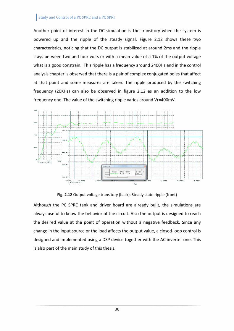
Fig. 2.12 Output voltage transitory (back). Steady state ripple (front) ...................................... 30
Fig. 3.1 Schematic of a controlled converter system .................................................................. 31
Fig. 3.2 PC SPRC block diagram ................................................................................................... 32
Fig. 3.3 PC SPRC transfer function bode plot of gain and phase. The dashed plot is the reduced
third order transfer function ....................................................................................................... 33
Fig. 3.4 root locus of the digital plant ......................................................................................... 35
Fig. 3.5 Underdamped response at f=2435Hz ............................................................................ 36
Fig. 3.6 Gain and phase margins with a closed-loop gain G=0.0389. The system is unstable .... 37
Fig. 3.7 IIR filter structure ........................................................................................................... 37
Fig. 3.8 IIR filter design ................................................................................................................ 38
Fig. 3.9 Bode plot of the notch filter and its effect in the plant ................................................. 39
Fig. 3.10 Bode plot of the whole system and stability information ............................................ 41
Fig. 3.11 Matlab Simulink PC SPRC DC converter schematic ...................................................... 42
Fig. 3.12 Output voltage of the DC converter with a 100Ω load ................................................ 43
Fig3.13 Closed-loop Matlab Simulink® schematic for the DC converter .................................... 44
Fig. 3.14 Output closed-loop converter response with a step in the reference from 1.5V to 3V
..................................................................................................................................................... 45
Fig. 3.15 Simplified circuit ........................................................................................................... 47
Fig. 3.16 Reduced circuit with fundamental component approximation ................................... 48
Fig. 3.17 Bloc diagram of the AC system ..................................................................................... 50
Fig. 3.18 Bode plot of the inverter Plant ..................................................................................... 51
Fig. 3.19 Inverter plant exported to SISOtool. Rootlocus(left), gain plot(up-right), phase
plot(down-right) .......................................................................................................................... 53
Fig. 3.20 Bode plot with gain and phase margins of the inverter plant plus the PI controller ... 54
Fig. 3.21 Step response of the system (inverter plant plus PI controller) .................................. 55
Fig. 3.22 Rootlocus(left), gain plot(up-right) and phase plot (down-left) with zeros cancellation
..................................................................................................................................................... 56

Study and Control of a PC SPRC and a PC SPRI
10
Fig. 3.23 Open-loop AC inverter simulation schematic .............................................................. 57
Fig. 3.24 Inverter open-loop response ........................................................................................ 58
Fig. 3.25 Inverter closed-loop simulation schematic .................................................................. 59
Fig. 3.26 Output closed-loop inverter response with a step in the reference from 1V to 1.5V . 60
Fig. 3.27 Texas Instruments ® TMS320F28335 DSP ................................................................... 61
Fig. 3.28 Main loop flowchart ..................................................................................................... 65
Fig. 3.29 ADC interrupt flowchart (left). Timer0 interrupt flowchart (right). ............................. 65
Fig. 3.30 Feedback signal after the voltage divider..................................................................... 70
Fig. 3.31 A sample is taken in every edge of the yellow signal and the green signal the input to
the ADC ....................................................................................................................................... 75
Fig. 4.1 Capacitor used for the PC SPRI resonant tank ................................................................ 79
Fig. 4.2 Equivalent magnetic circuit of an E core ........................................................................ 80
Fig. 4.3 Inductor building process. E cores, plastic bobbins and copper wire. Detail of a finished
inductor ....................................................................................................................................... 82
Fig. 4.4 PC SPRI resonant tank hardware .................................................................................... 82
Fig. 4.5 PC SPRI modules schematic. Control board modules are marked in blue ..................... 83
Fig. 4.6 Schematic of an isolation amplifier used in the feedback isolation ............................... 86
Fig. 4.7 The control board ........................................................................................................... 87
Fig. 4.7 Pin connections in the control board ............................................................................. 87
Fig. 5.1 100Ω, 200W rated resistor used as the load for the PC SPRC ........................................ 89
Fig. 5.2 Up: 396Ω, 60W rated resistor used as the load for the PC SPRI. Down: 200Ω 400W
resistor used to test the change of load ..................................................................................... 90
Fig. 5.3 Input high voltage power supply with a parallel high capacitance to improve the output
big ripple...................................................................................................................................... 91
Fig. 5.4 The testing bench. Up left: Detail of the six boards: The upper one is the PC SPRI tank,
the one in the middle is its control board, on its left is the PC SPRC control board, the one on
the bottom-left corner is the PC SPRC tank, right next to it the feedback isolation and the green
board is the DSP. Bottom left: Measurements with a floating scope. Right: View of the overall
tested system with the programming laptop. ............................................................................ 92
Fig. 5.5 Response of the PC SPRC low voltage version to a change in the input ........................ 93
Fig. 5.6 PC SPRI low version regulated steady state ................................................................... 93
Fig. 5.7 Steady state regulated operation point for the PC SPRC without load .......................... 95
Fig. 5.8 Switching frequency ripple at the PC SPRC output with an operation regulated point of
150V ............................................................................................................................................ 95
Fig. 5.9 Demonstration of the efficiency calculation in the PC SPRC .......................................... 96
Fig. 5.10 PC SPRC output response to a change in the load from 400Ω to 200Ω with regulation
at 170V ........................................................................................................................................ 96
Fig. 5.11 PC SPRC output response to a change in the load from 200Ω to 400Ω with regulation
at 100V ........................................................................................................................................ 97
Fig. 5.12 Change in the voltage reference from an output regulation of 100V to 170V ............ 97
Fig. 5.13 PC SPRI operation point regulated at Vo=200Vp ......................................................... 98
Fig. 5.14 Demonstration of the efficiency calculation in the PC SPRI ......................................... 99
Fig. 5.15 PC SPRI output response to a change in the load from 400Ω to 200Ω with regulation
at 170Vp ...................................................................................................................................... 99

Study and Control of a PC SPRC and a PC SPRI
11
Fig. 5.16 PC SPRC output response to a change in the load from 200Ω to 400Ω with regulation
at 170Vp .................................................................................................................................... 100
Fig. 5.17 Change in the voltage reference from an output regulation of 170Vp to 220Vp with a
400Ω load .................................................................................................................................. 100

Study and Control of a PC SPRC and a PC SPRI
12
CHAPTER 1: Introduction
One can start understanding the importance and influence of power electronics when
thinks about all different kind of electrical powered products in the market, all of them
having its own power converter, designed to provide a stable output at a certain value
from the raw power provided by the electrical grid or any energy storage device. One
also can find a very large power necessities range, starting at some mW for some low
power electronic consumers to some KW or even MW for industrial machinery.
Classical and traditional power devices such as lineal transformers or even some kind
of nowadays used SMPS (Switching Mode Power Supplies), need quite big magnetic
components, the losses are meaningful thus the efficiency could not be the desired
one so a right cooling system is a must or the size of the full system is not the
appropriate. For example, one big group inside SMPS are the hard-switching PWM
based converters, where a direct current or voltage is switched at a certain frequency
and filtered to obtain a DC voltage value different than the input changing the time of
the “on” and “off” states of the switch. Due to the non-idealities of the switching
square waves, voltage and current are at a positive value every switching time leading
to power dissipation so, losses are present in these systems and although they are
suitable for low or medium power consumption devices, they could be really hard to
implement in a high power system where an efficiency higher than 90% could be
desired. For these high power, high efficiency situations, a group of SMPS called
Resonant Converters is widely used due to their inherit soft-switching characteristics
and thus the high efficiency that it implies. The soft-switching is based on lowering
down to zero the voltage (Zero Voltage Switching) or the current (Zero Current
Switching) before the switch occurs, and this is achieved thanks to the sinusoidal
waveforms of voltage or current between the switches that the resonant tanks provide
discharging the drain-source capacitance of the switches through the series
inductance, so a higher efficiency is obtained, the switching frequency can be
increased to thousands or even some MHz so consequently magnetic components are

Study and Control of a PC SPRC and a PC SPRI
13
reduced and EMI’s are also decreased in comparison with the hard-switching based
converters.
1.1. Objectives and description
The aim of this project is to obtain a regulated high voltage AC output of 10KVp and a
frequency of 20KHz with a high voltage DC offset between 20KV and 50KV using 1:50
and 1:100 transformers respectively and an input around 300V. For this purpose,
resonant converters are chosen since the power of the system is going to be around a
thousand of watts and efficiency needs to be as high as possible. A DC-DC converter
and a DC-AC inverter are designed as well as their own controllers. It is needed to say
that the DC-DC resonant tank as well as its switching hardware was already built from
a previous PhD work but the controller software was not included. A parallel thesis is
focused on the study and design of the inverter but this specific work analyzes,
simulates and implements the stability and control of both, the DC converter and AC
inverter and describes the building process. A stable DC and AC outputs are desired
with a less than a 1% ripple in the first case and a fast response to a change in the
input or load in both.
There are different kinds of resonant circuits based on the resonant tank
configurations: Series Resonant Converter (SRC), Parallel Resonant Converter (PRC)
and Series-Parallel Resonant Converter (SPRC). Among these three topologies, the
SPRC shares the advantages of both the SRC and PRC, being the selected one for this
project. The control of the SPRC could be done either by frequency or phase. The
frequency controlled SPRC requires just a half bridge configuration compared to the
phase controlled one, that requires a full bridge in order to obtain two signals where
the difference of phase between them is the control variable. The advantage of the
phase control is that the switching frequency remains constant so it is better for the
output filter of the DC-DC converter or obviously is a required constrain in the case of
an inverter with a permanent output frequency. Also the efficiency of phase controlled
systems is not related with the control variable in contrast with frequency controlled
ones where the efficiency varies with it. Due to those facts, phase control is the
selected type in this project. There is also another reason to choose phase control and

Study and Control of a PC SPRC and a PC SPRI
14
it is because of the capability of some phase controlled converters, for example the
Phase-Controller Series Parallel Resonant Converter (PC SPRC), described and
introduced in [1], to provide inductive loads for the switching devices in both legs of
the full bridge if working over resonance. Thus, the reverse recovery currents through
the anti-parallel diodes in the switches are minimized and the power losses are
reduced having also a voltage fed system as it is desired.
Both the Phase-Controlled Series-Parallel Resonant Converter (PC SPRC) and Phase-
Controlled Series-Parallel Resonant Inverter (PC SPRI) open-loop circuits are
introduced and simulated with PSpice® so their operation point can be measured. This
is done previously to the building of the magnetic components of the inverter tank.
The inductive components are manually built so the data obtained from the
simulations is useful to do a safe design knowing the maximum currents circulating
through them. The design of the inductors is also described in this thesis.
1.2. The control of the PC SPRC and PC SPRI
For a control analysis and design of the closed-loop, the converter plant model is the
first thing needed. The model analysis of the PC SPRC is difficult because it leads to a
high-order non-linear equation due to the switches and many dynamic components
present in the circuit. Different methods have been used to describe the behavior of
the SPRC, but when phase control is desired, some are not suitable. For both systems,
converter and inverter, the extended describing function method is adopted to analyze
the small-signal model also applying the fundamental frequency approximation
knowing that the resonant tank is fed with the switching frequency. By decomposing
the sinusoidal quantities into d-q components, a nonlinear high-order model is
developed and linearized around the operation point of the converter. After this, a
reduction technique is applied to try to get a lower-order model.
In order to implement the closed-loop amplitude control of the AC and DC outputs, a
DSP device is used in place of the analog option. When this project was started, a DSP
controller for the PC SPRC was designed and used for the first time in this kind of
circuit but the code could not be found so a new controller was designed for both
inverter and converter operating just with just one DSP. Because digital devices evolve

Study and Control of a PC SPRC and a PC SPRI
15
very fast and the project was forgotten for a few years, a new DSP device has been
used. Specifically, the TMS320F28335 from TI® is the one used to control the system. It
uses a C2000 32 bit MCU running at 150MHz and provides the user with Timer, ADC
and PWM modules, inter alia, being those the basic ones used here. This thesis
presents the design procedure of the control as well as the description of the DSP
algorithm, where the zero-order holder (ZOH) and the controller delays have been
taken into consideration. Two Proportional-Integral (PI) controllers are designed and
implemented. For the case of the DC-DC converter, a sampling frequency higher than
the switching one should not be necessary because is useless to make more than one
change of the control variable in the same switching period. Nevertheless, in this work,
a much higher sampling frequency is used for the DC converter with more than one
reason that will be discussed along this text in the following chapters. By the other
hand, the inverter control justifies the fact of using the highest possible sampling
frequency and never lower than twice the fundamental harmonic (as the Nyquist
theorem says) to have a close representation of the analog sinusoidal output signal.
Furthermore, the used DSP cannot sample negative values so the AC negative half-
period is already lost in a sampling signal period. Because the need of the calculation
of the RMS value to control the AC output amplitude and the impossibility of sampling
the negative values of the signal, a new method has been thought and implemented
for the first time, which includes a zero cross detection and differentiation of positive
and negative values. Regarding the control input signal, there are some considerations
taken into account and some digital notch filters have been designed with Matlab® and
tested to troubleshoot different kind of problems with certain input frequencies that
could make the system unstable or that were simply interferences from the resonant
tank. Also different techniques to manage the processes running in the DSP have been
tried and are going to be discussed as there was an idea of using a Real Time Operating
System (RTOS) to execute two independent processes involving the two controllers so
the SYS/BIOS RTOS from Texas Instruments® was implemented with the DSP.
1.3. Application
Finally the system has being tested in a high voltage version with a DC output
regulation around 350V in the primary and a 1:100 transformer and a 200Vp AC output

Study and Control of a PC SPRC and a PC SPRI
16
in the primary with a 1:50 transformer. The final application of this high voltage system
is an air cleaning precipitator, where the AC signal from the inverter is superposed to
the DC voltage so a final sinusoidal signal of 10KVrmc with a 35KV DC offset is applied
between two electrodes. The polluted air running through those electrodes is cleaned
by attraction of the dust particles thanks to the high voltage. Some problems have
been worrying the precipitator companies since the load of the system is unstable and
always changing through a wide range of values. This makes the converters to work
with high loads and a sudden of very low loads and even shorts produced by the break
of the dielectric of the air. The aim is to prevent these shorts using a spark control with
maybe artificial intelligence techniques so the system reacts with a fast response even
when a short is present in the output.
1.4. Thesis overview
This thesis is divided in six chapters focused in different aspects of the project. In
chapter two the resonant converters are introduced as well as the converter and
inverter open-loop topologies chosen in this project, which are also simulated using
PSpice®. Chapter three focuses in the analysis of the stability of both PS SPRI and PC
SPRC and proposes a designed linear controller for both that are also simulated using
Matlab® and implemented using Code Composer Studio® in a Texas Instruments®
TMS320F28335 DSP. Chapter four leaves the theory from chapter two and software
from chapter three and focuses on the hardware implementation describing the work
that has been realized to build the PC SPRI both the resonant tank and the control
board. Finally chapter five presents the experimental results obtained in the overall
system leading the conclusions to chapter six.

Study and Control of a PC SPRC and a PC SPRI
17
CHAPTER 2: Description of the PC SPRI and
PC SPRC
Resonant power converters have been studied since the 80’s as a chance to increase
the working frequency in this field of electric and electronic engineering. This interest
on raising the switching frequency in converters lies in the idea of making the
components smaller since the transformers, filter inductors and capacitors are reduced
in value and weight when the operating frequency is increased. Usually the bandwidth
of the control loop of a converter system is determined by the corner frequency of the
output filter hence to have fast response negative feedback controls a high operating
frequency is also desired. Widely used PWM converters are not suitable for this new
purpose since they present power losses charging and discharging the MOSFETs
switching devices in every turn-on and turn-off states caused by the simultaneity of
voltage applied and current running through the device. For this reason the maximum
frequency in PWM converters is limited by the maximum dissipation power of the
MOSFETs or by the efficiency desired by the designer.
The resonant power converters are based in a switching circuit and a resonant tank in
the case of a DC-AC inverter and also a rectifier if a DC-DC conversion is desired. The
first block is composed by MOSFET or IGBT devices (depending the application, power
rating…) used to switch a power source creating a square waveform at the input of the
resonant tank with amplitude equal to the value of the source. The resonant tank acts
like a filter that just allows at the output the frequency component at which it
resonates and filtering all the rest. If the MOSFETs or IGBTs are switched close to the
resonant frequency, the output of the tank is a sinusoidal wave with the same
frequency as the fundamental of the squarewave at its input. The further the switching
frequency is from the resonant one, the smaller the gain of the tank is what is the FM
modulation principle used in this kind of converters. A schematic of a general half-
bridge resonant inverter is depicted in figure 2.1. Where IGBT1 and IGBT2 are the
devices used to switch the DC source creating the square waveform in Va. If the

Study and Control of a PC SPRC and a PC SPRI
18
switching is done close or at the resonant tank resonant frequency, the load sees a
sinusoidal waveform of the same period.
Fig. 2.1 General schematic of a half-bridge resonant inverter
The dotted line coming from the output of the resonant tank in figure 2.1 means that it
might or not be connected depending on the topology of the tank. There are three
possible different topologies that can be used: Series Resonant Converter (SRC),
Parallel Resonant Converter (PRC) and Series Parallel Resonant Converter (SPRC). The
SRC tank provides a current output to the load while the other two provide a voltage
output. These topologies are represented in figure 2.2.
Fig. 2.2 Three topologies of resonant tanks: series (left), parallel (middle) and series-parallel
(right)
If the resonant tank is designed to have a high loaded quality factor for the desired
range of loads (e.g QL ≥ 2.5), the current through the circuit can be considered a
sinusoidal wave as the rest of harmonics are rejected by the tank and hereby
neglected. Figure 2.3 illustrates the input voltage (red) and current (blue) to the tank.
In this case, the frequency which the switches are turned on and off coincides with the
resonant frequency of the tank thus the current and the input voltage are in phase.
This means that every time there is a switching state in the transistors, the current
Study and Control of a PC SPRC and a PC SPRI
19
value is zero thus there are ideally no power losses. Actually, square waves are never
ideal and there is always a delay between on and off states but as the derivative term
di/dt is small during these transitions, the losses are much smaller than in the case of
the PWM.
Fig. 2.3 Current (blue) and voltage (red) at the input of the resonant tank for fs=fo
In real applications is usually a difficult task to keep a fix switching frequency, even
more if the control of the output is designed using a half-bridge topology, where the
control variable is actually the switching frequency due to the variation of the gain of
the system with it (FM modulation). For this purposes, an operating range of
frequencies above the resonance are usually employed where the gain slope is
negative thus the higher the frequency the lower the gain. When the switching
frequency is above the resonance, the tank acts as an inductive load making the input
current sine waveform lead the voltage, as is depicted in figure 2.4, with a certain
phase ψ that increases with a bigger frequency difference.

Study and Control of a PC SPRC and a PC SPRI
20
Fig. 2.4 Current (blue) and voltage (red) at the input of the resonant tank with fs>fo
When the transistors are switched from the off to on state the circulating current is
negative thus forced to go through the antiparallel diode of the MOSFET or IGBT
resulting in a zero turn-on switching loss or Zero Voltage Switching (ZVS) as the
transistor is shorted by the diode (actually it is forced to the forward diode voltage that
is small enough to consider it a short). In the turn-off state, current and voltage
overlap in a positive value resulting in the turn-off losses that can be reduced using a
shunt capacitor in one of the transistors and using a deadtime in the drive gate voltage
signals. For a switching frequency below the resonance, the same theory is applicable
and zero turn-off losses are obtained. The difference is that in the turn-on state there
are some effects that make this kind of operation a worse choice than the explained
before. These effects yield in high di/dt when the antiparallel diodes turn off
generating high reverse-recovery current spikes [2].
This ZVS inherit characteristic is what make resonant converters interesting and why
they are preferred over PWM based ones within high efficiency or high frequency
applications. Nowadays one can find some literature concerning about the analysis of
every resonant tank configuration and regarding all about resonant power converters
and its applications [2] [3] [6].

Study and Control of a PC SPRC and a PC SPRI
21
Once reviewed some of the basics about resonant converters, the circuit that is
desired to design is presented below. The specifications that are tried to achieve in this
thesis consist of a regulated high voltage DC output of 30KV with a coupled and also
regulated AC component of 10KVp and 20KHz for a load that is around 1MΩ but may
vary in function of time having a wide range of values that can also include a short
circuit. The ripple of the DC output signal is considered to be less than the 1% of the DC
value. Because the efficiency is always a good constraint to take into account even
more if working with high power like in this project and because some of the designs
were already started years ago concerning the development of the DC converter,
resonant converters are chosen to achieve the requirements of the proposed system.
The general schematic of the circuit that is desired to build is shown in figure 2.5. It
consists of two resonant inverters fed by a common input power source and loaded
with transformers to step up the voltage and also isolate the grounds to have a proper
connection between them. After one of the transformers, a rectifier permits to have a
DC output voltage that is connected in series with the second transformer providing
the AC signal. The half circuit composed by one resonant tank and the corresponding
switches, the transformer and the rectifier is called the DC converter because makes a
DC-DC conversion while the other system consisting of the other resonant tank and
switches and the other transformer is called the AC inverter due to its DC-AC
conversion. The series output connection is loaded with an electrostatic precipitator
that brings the variable impedance. An electrostatic precipitator is a device consisting
of two electrodes facing each other leaving a gap where dirty air may circulate and
where the dust particles should be retained by electrostatic forces created by the high
voltages between these two electrodes.

Study and Control of a PC SPRC and a PC SPRI
22
Fig. 2.5 General schematic of the desired system
2.1 The AC inverter
As it was discussed before, the FM modulating of the switching frequency slightly
above the resonance yields in a range of different gains in the tank that permits a
control of the output with a change in the input voltage or in the load. The
disadvantage of this kind of control is that the output sinusoid has the same frequency
as the fundamental harmonic of the square waveform created by the switches,
therefore both are modified if the switching frequency is changed. If a fixed operating
frequency is desired, a full bridge configuration can be used in order to maintain the
frequency, and control the output signal amplitude by the difference of phase applied
by the bridge over its two legs. Any half-bridge resonant tank topology can be modified
and converted into a phase controlled system by doubling the half bridge and resonant
tank in a horizontal mirroring manner from the load section. This means that both
sides of the load have the same resonant tank that can be series, parallel or series-
parallel and a half bridge switching network. This idea is illustrated in figure 2.6

Study and Control of a PC SPRC and a PC SPRI
23
Fig. 2.6 Phase-controlled resonant inverter
Figure 2.6 shows how a phase-controlled inverter can be built using two symmetric
resonant tanks and four switching devices configuring a full bridge. If nodes Va and Vb
have the same frequency and in-phase squared waveforms with an amplitude given by
the DC source, currents i1 and i2 are sinusoids with the same phase and amplitude,
what yields in a current over the load that is the addition of i1 and i2 with zero phase
and same frequency thus the output voltage is described in equation 2.1 where Ai1 is
the amplitude of current i1 and Ai2 the amplitude of i2.
= 1 + 2 · · cos (2.1)
If the phase between the square signals in Va and Vb is increased, currents i1 and i2
are also phase shifted [4] and the current amplitude yields to equation 2.2, where
I=Ai1=Ai2 and Φ is the phase between Va and Vb.
= 2 · · cos · cos (2.2)
Analyzing equation 2.2, the maximum and minimum applicable phases between both
legs of the resonant tanks are obtained as Φ=0º for a maximum gain (minimum phase)
and Φ=180º for a gain zero (maximum phase). This is not the only possible
configuration, for example tank topologies with output parallel capacitors and a series
output resistor behave as two sinusoidal sources connected to the load and the
controllability of the phase is opposite to the one before as for Φ=180º there is a
maximum gain and for Φ=0º the voltage output is zero. In all cases, the output voltage
amplitude has dependence with a phase between two signals that are totally
controllable and independent from the input, the load and the switching frequency.

Study and Control of a PC SPRC and a PC SPRI
24
This is one constraint for the AC inverter that is presented in this thesis so a Phase
Controlled system is chosen in the first instance.
Besides the configuration of the tank (series, parallel or series-parallel) and the control
variable used in the closed-loop (that can be the frequency for a half bridge
configuration or the phase for a full bridge), there are some different topologies of
inverters classified in classes D, E or D-E [2]. This thesis does not focus in the study of
the different topologies due to the wide biography about the subject. What is
interesting to mention is that both, the AC inverter described in this section and the DC
converter described below, are class D. One of the main advantages of class D voltage-
switching converters is the low voltage across the switching transistors, which is equal
to the input voltage. Since in this thesis the desired output voltage is considered a high
voltage, the input may be around some hundreds of volts. The higher the transistor
voltage ratings are, the bigger the equivalent on-resistant [2] thus the losses increase.
It is considered a good choice a class D inverter for the concerning purpose.
A class D Phase-Controlled Series-Parallel Resonant Inverter (PC SPRI) is presented as
the AC inverter designed to provide the 10KVp. Series-parallel is the chosen topology
because it shares advantages and characteristics from the series and the parallel. Since
the output load is not predictable because is function of the pollution in the running
air, and shorts may occur when the air dielectric is broken due to the high voltage
applied between two close electrodes, the series-parallel option is chosen as the SRC is
a bad idea to work with light loads and has no protection against short circuits. By the
other hand, the PRC is protected against short circuits as the gain decreases with the
load, but the circulating energy over the tank is high. The SPRC topology is also capable
to stand zero load conditions and reduces the circulating energy.
The PC SPRI is depicted in figure 2.7. It consists of four switching IGBT’s in a full bridge
configuration where the phase delay between the gate triggering signals in each
branch permits the phase controlling of the output. The output of the PC SPRI is
measured between the load resistor (RL) that is in parallel with the output capacitors
of the two SPI resonant tanks, making a unique 2Cp capacitor. The series elements of
both sides of the tank are the series inductor (Ls) and the series capacitance (Cs). A
Study and Control of a PC SPRC and a PC SPRI
25
resistive element is placed in series in both branches to characterize the Equivalent
Series Resistance (ESR) of these both elements. A DC input feeds both branches of
transistors and provides the needed power to satisfy the output necessities. The
resonant tank is designed to resonate at 19KHz and the pulse signals that control the
switches are configured at 20KHz so the turn-on losses are notably reduced. The load
resistor is the equivalent impedance that is connected to the output of the tank
through the transformer. For the AC inverter a 1:50 transformer is used thus if the
nominal impedance of the precipitator is 1MΩ, the equivalent load in the primary is
RL=400Ω.
Fig. 2.7 Schematic of the PC-SPRI
The analysis of the circuit in figure 2.7 and the design of the elements are widely
discussed in reference [4] that has been developed in parallel and at the same time as
this thesis. The final values of the elements from the tank are specified in table 1 of the
Appendix I.
2.1.1 Open-loop AC inverter simulations
To perform the open-loop simulations of the schematic in figure 2.7 the Orcad® PSpice
software is used. The schematic is drawn substituting the switches and DC input for
two square waveform sources connected at both branches of the tank, making it easy
just to test this part of the circuit configuring the sources as necessary (frequency,
rising and falling time…). The switching frequency is configured at 20KHz with a duty

Study and Control of a PC SPRC and a PC SPRI
26
cycle of 50%, no phase shifting and rising and falling times of 1us. An ESR of 0.01Ω has
been added as the nonidealities of the inductor and a value of 5Ω for the capacitor
ones. Figure 2.8 illustrates the Spice schematic that has been simulated with
commercial values for the components and a load of RL=400Ω and the steady state of
the open-loop circuit, where the current plot (black) in one of the series branches of
the tank has been multiplied by a factor of 150 to clearly show that in the desired
operation, the OFF state of the MOSFETs is switched to the ON state when the current
is negative thus the antiparallel diode is conducting and losses are ideally zero for this
case but not for the OFF to ON switch. This change of state signal (green) is provided
by the square wave sources that substitute the switching devices. The AC output is also
shown in the same figure (red) having a peak voltage of Vp=525V or a rms voltage of
Vrms=375Vrms for a Vin=300V so the maximum gain in open-loop is
G=375/300=1.237.
Fig. 2.8 Pspice AC inverter schematic (up). Plot of square branch input voltage (green), output
voltage (red) and current over one of the series branches increased a factor of 150 (black)

Study and Control of a PC SPRC and a PC SPRI
27
Besides the steady state operation, the transitory response is also observed and
depicted in figure 2.9 where the output takes around 0.5ms to stabilize.
Fig. 2.9 AC inverter open-loop output transient response
This simulation gives a close idea of how the AC inverter should behave for the
operating point it is designed for. Since a 1:50 transformer is used, the desired voltage
at the primary side is Vp=200Vp to reach a V=10KVp output and it does not match the
voltage in open-loop. Because of this reason and since there can be changes in the
load that affect the output voltage, a negative feedback, stability analysis and control
design is necessary. This is the main objective of this thesis and is explained in further
chapters.
2.2 The DC converter
A DC-DC resonant converter is based in a combination of a DC-AC inverter and a
rectifier that suppresses the alternating component using either a half or full wave
configuration. The DC converter used in this project was already proposed and
designed in [5] and its element values of the resonant tank are specified in table 2 of
Appendix I.
2.2.1 Open-loop DC converter simulations
The operation of the DC converter is similar to the AC inverter. It is composed of a
phase-controlled series-parallel resonant inverter and a full wave rectifier connected

Study and Control of a PC SPRC and a PC SPRI
28
to the output of the transformer that amplifies the voltage from the output of the
inverter. After the rectifier, an LC network creates a filter in order to obtain the DC
component in the output. Figure 2.10 shows the schematic of the Phase-Controlled
Series-Parallel Resonant Converter (PC SPRC).
Fig. 2.10 Schematic of the PC SPRC
As it was done for the AC inverter schematic, the ESR is also taken into account in the
DC converter in both the filter and the tank. The resonant tank was designed to
resonate at 19KHz with a 20KHz switching frequency achieving a gain of G=1 as the
input source and output of the inverter have the same value in the operation point
(300V). The bad point about having a unity gain is that the circuit is not going to be
able to step up the output if any the input voltage or load change and decreases it. A
1:100 transformer is connected between the inverter and the full-bridge rectifier
stepping up the 300V to 30KV at the output of the PC SPRC as it is desired in the
specifications of the project.
To simulate the PC SPRC in open-loop configuration, OrCAD® PSpice is used again with
the schematic shown in figure 2.11 (up)- where R9 and R10 are big resistors just
necessary for the software to converge in a solution but not affecting the final result.
The switches have been substituted by square wave sources that provide the same

Study and Control of a PC SPRC and a PC SPRI
29
inputs to both branches of the resonant tank configured as 20KHz waves with 50% of
duty cycle and no phase shift. The output load is RL=100 Ω that is equivalent to the
resistance in the primary of the transformer having n=100 and a load of 1MΩ at the
output of the total circuit.
Fig. 2.11 Pspice DC converter schematic (up). Plot of square branch input voltage (red), DC
output voltage (green), current over one of the series branches increased a factor of 50 (black)
and AC tank output signal (blue)
Looking at the results of the simulation in figure 2.11 (down) a ZVS (Zero Voltage
Switching) is achieved from the OFF to ON state (red) as the current (black) is negative
and the switches are shorted by the antiparallel diode. The blue plot shows the voltage
at the parallel capacitor 2Cp before being rectified and filtered to obtain the DC output
(green), that matches the value of the input source with the maximum gain of the tank
so the gain G=1 is well designed for this point of operation.
Study and Control of a PC SPRC and a PC SPRI
30
Another point of interest in the DC simulation is the transitory when the system is
powered up and the ripple of the steady signal. Figure 2.12 shows these two
characteristics, noticing that the DC output is stabilized at around 2ms and the ripple
stays between two and four volts or with a mean value of a 1% of the output voltage
what is a good constrain. This ripple has a frequency around 2400Hz and in the control
analysis chapter is observed that there is a pair of complex conjugated poles that affect
at that point and some measures are taken. The ripple produced by the switching
frequency (20KHz) can also be observed in figure 2.12 as an addition to the low
frequency one. The value of the switching ripple varies around Vr=400mV.
Fig. 2.12 Output voltage transitory (back). Steady state ripple (front)
Although the PC SPRC tank and driver board are already built, the simulations are
always useful to know the behavior of the circuit. Also the output is designed to reach
the desired value at the point of operation without a negative feedback. Since any
change in the input source or the load affects the output value, a closed-loop control is
designed and implemented using a DSP device together with the AC inverter one. This
is also part of the main study of this thesis.

Study and Control of a PC SPRC and a PC SPRI
31
CHAPTER 3: The Control of the PC SPRC
A usual required constraint in a converter system is to keep the output voltage of the
system constant even if the input voltage or the load impedance change. Because in
most of the cases the output voltage value is function of the input and load, an
additional controller is needed to achieve this constraint. Figure 3.1 represents this
brief idea:
Fig. 3.1 Schematic of a controlled converter system
This chapter analyzes the design of the DC-DC and DC-AC converter controllers, from
the schematic of the hardware circuit to the program of the software and shows the
simulation results obtained in closed-loop.
3.1. Design of the PC SPRC control
The first step when designing a controller for a system is to decide between working in
the analog or digital world. Using some kind of digital controller could be expensive if
the controller to design is a simple lineal one, but for nonlinear techniques or complex
controlling, designing an analog controller could be tough and require a bit of test and
error since sometimes they do not behave as expected. In this case, this decision was
already taken and a DSP was previously used to control de voltage output of the DC-DC
converter. Because this project started long time ago, the digital devices evolve so
quickly and there was no reference about the software used previously, a newer DSP
has been used to program the control.

Study and Control of a PC SPRC and a PC SPRI
32
The TMS320F28335 is a Texas Instruments® DSP that works with a 150MHz CPU clock,
has an ADC module and 6 PWM modules that can be synchronized, besides obtaining
the complementary waveform of every PWM module. Those characteristics make the
chosen DSP a good option to work with.
Once decided to work with a digital system to control the voltage in the output, the
transfer function in the Z plane is obtained and the stability of the closed-loop is
analyzed. First of all, the block diagram of the system is represented figure 3.2.
Fig. 3.2 PC SPRC block diagram
As can be seen in figure 3.2, a ZOH is necessary at the output of the digital system and
an ADC at the input. Also isolation is required between analog and digital systems to
avoid big current return peaks from the converter and because of different groundings
between the converter output and the DSP. In this case, taking benefit of the use of a
DSP, all the filtering requirements have been implemented inside it. Finally, the ‘α’ bloc
represents the voltage divider that steps-down the output voltage that would be too
high to be connected directly to the DSP.
3.1.1. Analysis of the PC SPRC plant
Next step is to get the model of the plant, in this case the DC-DC converter model.
According to [1], the continuous reduced model transfer function of the PC SPRC is as
follows in equation (3.1). This equation is based in a gramian reduction from the real
eighth order model one:
Gp(s)= . !"#$%&'.(!"!$).(*"'
$+),.#"'$%).##"!$),.-(" (3.1)
Study and Control of a PC SPRC and a PC SPRI
33
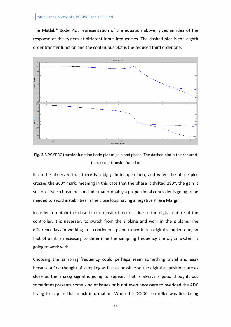
The Matlab® Bode Plot representation of the equation above, gives an idea of the
response of the system at different input frequencies. The dashed plot is the eighth
order transfer function and the continuous plot is the reduced third order one:
Fig. 3.3 PC SPRC transfer function bode plot of gain and phase. The dashed plot is the reduced
third order transfer function
It can be observed that there is a big gain in open-loop, and when the phase plot
crosses the 360º mark, meaning in this case that the phase is shifted 180º, the gain is
still positive so it can be conclude that probably a proportional controller is going to be
needed to avoid instabilities in the close loop having a negative Phase Margin.
In order to obtain the closed-loop transfer function, due to the digital nature of the
controller, it is necessary to switch from the S plane and work in the Z plane. The
difference lays in working in a continuous plane to work in a digital sampled one, so
first of all it is necessary to determine the sampling frequency the digital system is
going to work with.
Choosing the sampling frequency could perhaps seem something trivial and easy
because a first thought of sampling as fast as possible so the digital acquisitions are as
close as the analog signal is going to appear. That is always a good thought, but
sometimes presents some kind of issues or is not even necessary to overload the ADC
trying to acquire that much information. When the DC-DC controller was first being

Study and Control of a PC SPRC and a PC SPRI
34
designed, and there was still no clue about the inverter control, a sampling frequency
of 20 KHz was chosen. The reason for that chose was that is the same as the switching
frequency so it is considered more than enough to activate the control every period of
the switching, furthermore the bandwidth of the open-loop converter is around
3x10^4 rad/s or 5KHz so at least double that frequency is needed to avoid significant
bandwidth decrease, which is already fulfilled. Because the DSP works at a much
higher frequency than 20 KHz, and there was no success configuring the ADC at 20
KHz, the decision of working at 100 KHz was taken, acquiring 5 values and calculating
the main of those every time before activating the control, so it was done every period
with a more accurate measure. When the DC converter was designed and tested and
the AC inverter control was starting to be incorporated being part of the whole DSP
software, new tests where done with the ADC module finally succeeding in configuring
it at a sampling rate of 20Ksps but observing that the DC response becomes worse,
with an increase of the ripple at the output due to a coupled 20KHz signal in the
control signal from the resonant tank. Because of the need of a much higher sampling
frequency for the AC feedback signal and still keeping in mind the idea of the mean
value for the oversampled DC output, the ADC was configured to work at a frequency
close to 1MHz having a lot of instability in the DC output so the control constants had
to be so small that the control, if not instable, was very slow. So a balance between
stability and fast response had to be found and finally a sampling frequency of 200KHz
has been used for the ADC module, sampling both, the DC converter and AC inverter
and calculating the DC mean value every 10 samples so the control process is done just
once every switching period, thus from now on the sampling frequency of the DC
output is going to be supposed as if it was 20KHz for the system analysis.
Once the final sampling frequency for the ADC is established, so the rate of acquiring
the DC output is known, the Z plane digital transfer function of the PC SPRC is obtained
via Matlab® with the following command: Gz=c2d(Gs,0.00005,'zoh'), where “Gs” is the
continuous transfer function (3.1), the middle value is the time between samples and
‘zoh’ stands for Zero Order Hold or the way used to transform the function from plane
S to plane Z that takes into consideration its delay. The result is shown in equation
(3.2).

Study and Control of a PC SPRC and a PC SPRI
35
Gp(z)= .*##.%). *.).
.+&.-'.%).--.& .(, (3.2)
Moreover, taking into account that the DC signal is sampled 10 times in a period plus
the time the DSP needs to calculate the new phase for the control variable and change
the phase in the output, is equivalent to add a unit time delay to the loop because the
value calculated for the current step is not applied until the next switching period. This
is done by multiplying equation (3.2) times .. For all this, the final unity feedback
closed-loop equation of the converter becomes:
Gp(z)= .*##.%). *.).
./&.-'.+).--.%& .(,. (3.3)
3.1.1. The PC SPRC control analysis
The root locus of (3.3) is represented in figure 3.4 where one can observe that there is
a complex conjugated pole pair close to the unity circle.
Fig. 3.4 root locus of the digital plant
Figure 3.4 also represents some information about the influence of these paired poles,
being the damping factor an important point to have into account. This factor shows
how the response of the circuit is going to behave if the input is excited with a certain

Study and Control of a PC SPRC and a PC SPRI
36
periodic signal, for example a sinusoidal waveform. In this case, there is a damping
factor of ζ= 0.112 when the input angular frequency is 15.3Krad/s that is equivalent to
2435Hz. This is a quite underdamped response, with an overshoot of 70.2%. The
representation of this response in Matlab®, with a normalized frequency, shows how
the output is near the instability:
Fig. 3.5 Underdamped response at f=2435Hz
Analyzing more deeply the root locus from figure 3.4 in the Matlab® plot, it can be
observed that this conjugated poles move to the unity circle when the gain of the
system is G=0.0389 what means that with a very little gain the system has a critical
damping (ζ=0) at a certain frequency, and it becomes unstable if the gain increases
(ζ<0). This can be also demonstrated with the bode plot of the open-loop plant where
there is an overshoot at w=15.3Krad/s induced by these paired poles, besides the gain
around the -180 degrees phase is very close to zero, what makes it to behave near
instability in a unity gain closed-loop. Figure 3.6 shows this bode plot and also the bode
plot with a gain of G=0.0389 where the gain margin and phase margin have been
added to demonstrate that the system is unstable as the gain of the open-loop is 0dB
when the phase is -180º, what becomes in an infinite gain for a unity close-loop
system.

Study and Control of a PC SPRC and a PC SPRI
37
Fig. 3.6 Gain and phase margins with a closed-loop gain G=0.0389. The system is unstable
To solve the problem of the overshoot, an IIR (Infinite Impulse Response) notch filter is
designed. Taking advantage of the use of a DSP, a digital filter is chosen over its analog
counterpart and integrated with the control. The filter parameters are obtained with
the Matlab® tool called ‘FDAtool’ and used inside the DSP where the digital filter was
programmed. The next figure represents an IIR filter:
Fig. 3.7 IIR filter structure

Study and Control of a PC SPRC and a PC SPRI
38
The structure shown in figure 3.7, is the one that has been implemented within the
software. The a[x] and b[x] are the coefficients of the filter, and the Z-1
blocks are one
loop delays, what means that is necessary to store the previous values for the next
loop. In this occasion, an order two filter was enough to get a good attenuation and
bandwidth at the specified frequency. As can be seeing in figure 3.8, the single notch
digital filter is designed with FDAtool, specifying a sampling frequency of 20Khz, a
centered notch frequency of 2435Hz (where the two complex paired poles where
affecting), and a bandwidth of 1KHz.
Fig. 3.8 IIR filter design
With those specification and after some tries and modifications of the bode plot, the
parameters of the notch filter are obtained: A = [1 -1.9533 0.9623] and B = [0.9812 -
1.9533 0.9812]. The purpose of this is to modify the whole system bode plot and the
root locus in order to have stability with a good phase and gain margins.
To study the effect of the filter in the system its transfer function is obtained from the
general IIR transfer function in (3.4) and described specifically in (3.5) as a digital t.f. in
the Z plane .
01 = ∑ 34.54657489∑ :;.5;<57;89
(3.4)

Study and Control of a PC SPRC and a PC SPRI
39
0=>1 = .#'.5%&.--.57).#& .!*(.5%& . #.57 (3.5)
Figure 3.9 shows the bode plot of the filter and its effect in the plant. It can be
observed that the overshooting behavior of the complex paired poles has been
cancelled by positioning the new zeros very close to them. What can also be noticed is
that the system is still unstable since the phase crosses -180º (0º in the figure) when
the gain is still positive so the phase margin is negative. To solve this, the gain should
be lowered to 0dB before there is an inversion of phase and this is done with a
proportional gain smaller than unity.
Fig. 3.9 Bode plot of the notch filter and its effect in the plant
To know the maximum proportional gain that makes the system become stable, the
positive gain at phase 180º must be known. As figure 3.9 shows, this gain is 18.4dB
that is equivalent to G=8.3176 in linear terms. The reciprocal of that gain is the
maximum proportional gain applicable to the system and that never should be used, as
that is the one that makes a gain G=0dB when the phase is 180º so for that reason the
proportional gain should be: Kp< 0.12022

Study and Control of a PC SPRC and a PC SPRI
40
The smaller the Kp becomes, the higher the Gain Margin is but also the gain of the
system decreases so the response becomes slower. With all these characteristics, the
proportional gain constant is chosen for a GM bigger than 9dB (as a usual constraint)
and to accomplish this, Kp=0.035 what leads to a GM=10.7dB and a phase margin
PM=112º.
At the same time, in order to remove the steady state error in closed-loop, an
integrator is also combined with the proportional gain resulting in a PI controller that
can be represented, using the Tustin bilinear transformation method, as described in
equation (3.6) where Kp is the proportional gain, Ki -the integral gain and Ts is the
sampling period (50µs).
?@1 = A@ + A ∗ C.).& (3.6)
To obtain the integral gain value, various methods are present in the literature. One of
them, the Ziegler-Nichols method, is widely used and it implies some empirical and
mathematical techniques. In this thesis, a more empirical technique is used where the
gain is increased until a value where the system response starts to oscillate so a
maximum gain value is obtained. The next step is to reach a good compromise
between the steady state error and the transitory. If the Ki value is too big, the steady
state error is very small or ideally zero but the response of the system is slower. By the
other hand, if the integral gain is too small, the response is good and the control is very
fast but the steady state error is big. Finding the correct value is not always easy and
requires some time of experimentation and deep analysis of the output signal and
different variables used inside the digital control. After some empirical simulation
testing, a final value of Ki=40 is taken as a good consideration. Equation (3.7)
describes the final PI controller equation in continuous mode and (3.8) describes it in a
discretized way for an implementation in a digital device as the DSP used in this thesis.
D = 0.035 ∗ HIII + 3800 ∗ K HIIIL (3.7)
DA = 0.035 ∗ HIIIM + 0.095 ∗ ∑ HIIIOMOP QR = 0.00005R (3.8)

Study and Control of a PC SPRC and a PC SPRI
41
The final unity closed-loop system is obtained by multiplying the plant in (3.2), the Z-1
delay, the notch filter in (3.5) and the PI controller in (3.6), so the final result is shown
in the next equation and its bode plot in figure 3.10, where all the stability information
provided by the command ‘allmargin’ from Matlab® is also included and demonstrated
that is a stable system.
?ST1 = 0.02044 ∗ 1* − 0.00363 ∗ 1# − 0.0011 ∗ 1' − 0.03689 ∗ 1 + 0.06516X − 0.03422X( − 3.478X, + 5.115X* − 3.976X# + 1.587X' − 0.2629X + 0.01482X
(3.9)
Fig. 3.10 Bode plot of the whole system and stability information
3.1.2. Simulations
Once the system is designed, some tests have been worked out to analyze the closed-
loop response. For this purpose, Matlab Simulink® is used due to its discrete simulation
capabilities, its wide library and its good combination with the Matlab® kernel that has
been widely used in this thesis.
The open-loop PC SPRC schematic in figure 3.11 is built at a first instance to check if
the results are similar to the ones obtained with PSpice® in chapter 2. As can be seen
in this case, the switching devices are IGBT’s gate controlled by a generic pulse
generator, creating a square wave at both branches of the tank, configured in this case
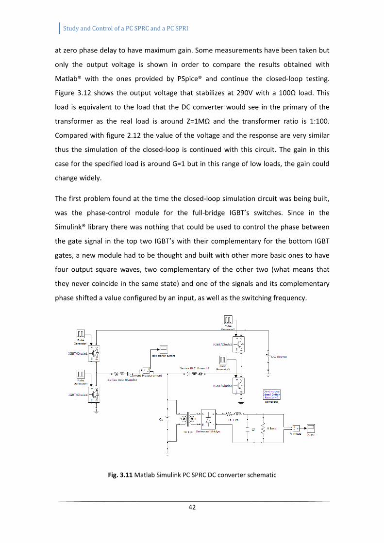
Study and Control of a PC SPRC and a PC SPRI
42
at zero phase delay to have maximum gain. Some measurements have been taken but
only the output voltage is shown in order to compare the results obtained with
Matlab® with the ones provided by PSpice® and continue the closed-loop testing.
Figure 3.12 shows the output voltage that stabilizes at 290V with a 100Ω load. This
load is equivalent to the load that the DC converter would see in the primary of the
transformer as the real load is around Z=1MΩ and the transformer ratio is 1:100.
Compared with figure 2.12 the value of the voltage and the response are very similar
thus the simulation of the closed-loop is continued with this circuit. The gain in this
case for the specified load is around G=1 but in this range of low loads, the gain could
change widely.
The first problem found at the time the closed-loop simulation circuit was being built,
was the phase-control module for the full-bridge IGBT’s switches. Since in the
Simulink® library there was nothing that could be used to control the phase between
the gate signal in the top two IGBT’s with their complementary for the bottom IGBT
gates, a new module had to be thought and built with other more basic ones to have
four output square waves, two complementary of the other two (what means that
they never coincide in the same state) and one of the signals and its complementary
phase shifted a value configured by an input, as well as the switching frequency.
Fig. 3.11 Matlab Simulink PC SPRC DC converter schematic

Study and Control of a PC SPRC and a PC SPRI
43
Fig. 3.12 Output voltage of the DC converter with a 100Ω load
The final idea of building the phase shifting controller module is not trivial, and after
various tries and different ways to do it, a final schematic is presented in Appendix II.
The idea is creating the squarewaves from a cosinusoidal wave with the same time
reference for all four output signals. Because creating different sinusoidal forms being
able to change the phase and frequency is an easy task, the direct mathematical
definition of the cosine is applied as A·cos(2·π·f+φ) where ‘A’ is the amplitude of the
signal, ‘f’ is the frequency and ‘φ’ the phase. In the output signals, there is one signal
reference that all other three are referenced to, another signal that is the
complementary of the reference and for instance has always a phase of φ=pi, and two
other signals that are phased a variable value that is the control variable and one of
them also adds an extra φ=pi to be the complementary of the other one. Once the
sinusoidal phase and frequency controlled signals and their complementary ones are
obtained, just remains the method to convert them to square waves. The technique
used here, as the most effective one that has been tested, is based on the idea of
holding two samples of a period. In other words, the values of the sinusoidal signals
are held every time they reach a maximum and a minimum so a square wave is
obtained. More specifically, the sample and hold that is used is triggered by a hit
crossing module that detects every time the sinusoidal wave is at the 99% of the

Study and Control of a PC SPRC and a PC SPRI
44
positive and negative peak because if it was the exact amplitude (100% of the peak),
the digital values of the simulation make that sometimes the exact peak is not reached
and a hit crossing is missed. Finally, the last step is to use a saturation bloc to have an
output square wave signal between 10V and 0V to correctly switch the IGBT’s.
Once the phase controller module is included, the loop is closed as described
previously. This includes the notch filter transfer function, the unity delay and the PI
controller. Also an additional gain smaller than the unity is used to multiply the output
in order to compare it to a reference of 1.5V, simulating what is used in the real circuit
due to the voltage limit of the input to the ADC module of the DSP. The consequence
of this additional gain is that the bode plot is moved down a factor equivalent to the
value of the gain so in order to have the same response, the values of the proportional
and integral constants have to be divided by the same gain. As the reference from the
DSP, thus the one used in the simulation, is 1.5V and the desired output is 300V, the
additional gain bloc is calculated as β=1.5/300 = 0.005. The final closed-loop schematic
built in Matlab Simulink® is shown in figure 3.13 where the switching frequency is
finally configured at 20KHz, that is a bit above the resonant one and the IGBT’s are
gate controlled by the full-bridge phase controller explained before, where the phase
input is the control variable that the PI provides This schematic can be observed with
more detail in Appendix VI.
Fig3.13 Closed-loop Matlab Simulink® schematic for the DC converter

Study and Control of a PC SPRC and a PC SPRI
45
The parameters of the simulation hve to be changed a little. In this case the maximum
step has to be small enough to have the square wave signals without aliasing problems
thus a maximum step of 1us is selected for further simulations. Figure 3.14 shows the
output signal in closed-loop. The PI parameters have been tuned to have an
underdamped response with a settling time as short as possible and avoiding a big
overshoot and the final values for the simulation taking into account the new gain
β=0.005 in the loop are: Kp=2 and Ki=8000 . In the same simulation figure is shown a
step response of the system when the reference goes from 1.5V to 1V so the output is
lowered from 300V to 200V. There has been also some interest to see the response of
a change in the output but the Simulink® power blocs used for the IGBT’s did not allow
any connection of switches or step functions to their collector terminals. The big
overshoot at the beginning of the simulation represents the power-up of the system,
but the controller is fast enough to step the output down in less than 7ms. When the
reference is changed at t=0.05s, the transient response lasts around 2ms, something
reasonable for this kind of controller and application. About the ripple observed, it
corresponds to the same ripple in open-loop, with an amplitude of about 1.5V and a
frequency of 2000Hz.
Fig. 3.14 Output closed-loop converter response with a step in the reference from 1.5V to 3V
Study and Control of a PC SPRC and a PC SPRI
46
The conclusion about the analysis and stability of the PC SPRC closed-loop brings a
good reference point to continue with the real implementation of the controller where
some other blocs are needed, like the digital filtering. Nevertheless, all the blocs and
the PI controller can be developed digitally with a DSP and that is what is done and
explained in further section of this thesis.
3.2. Design of the PC SPRI control
Once there is a positive conclusion about the DC converter closed-loop analysis, the
AC-inverter is put under the scope and analyzed in the same way. Because both power
converters are going to be used in the same system, it is obvious to take benefit of the
use of a DSP from the DC-converter control and try to make the AC-inverter controller
with the same requisites. In this case, the software of the DSP includes both controllers
working at the same time.
When the decision of the digital controller is done, next step is obtaining the whole
system open-loop transfer function and analyze it in unity gain closed-loop. For the AC-
inverter, the bloc diagram is the same already presented for the DC converter in figure
3.3 so, as it was explained before, the first thing needed for the stability analysis is to
obtain the plant of the system, in this case the transfer function that describes the
behavior of the resonant tank and the switches.
3.2.1. Analysis of the PC SPRI plant
The following lines summarize how the transfer function of the PC SPRI is obtained
with not an extreme detailed explanation. For a more detailed and developed equation
solving, one can read reference [4] that has been developed in parallel with this thesis
and is focused in the design and modeling of the inverter.
Before heading into the analysis of the inverter transfer function of the circuit shown
in previous chapters (view figure 2.7), some approximations have been considered
from reference [5]. Following that dissertation, the PC SPRI tank is split in two identical
SPR ones and just one of them is studied, taking into account that the output current
through the capacitor should be doubled as is illustrated in figure 3.15.

Study and Control of a PC SPRC and a PC SPRI
47
Fig. 3.15 Simplified circuit
As shown in the previous image, a series resistor is added to the tank representing the
series equivalent resistance of the inductor (ESR). From the circuit in figure 3.15, the
sinusoidal approximation is applied substituting the resonant tank quantities by their
fundamental components resulting in the circuit shown in figure 3.16, where Vic is the
common mode input of the reduced model tank resulting from decomposing both
sinusoidal inputs at both sides of the full PC SPRI resonant tank into D-Q phasors and
discriminating the differential parts, as they cancel out each other at the output [5],
thus Vic can be expressed as (3.10)
OZ = [ · cos · sin (3.10)
From equation (3.10), there can be observed a couple of details. First of all, the
common mode equation is, obviously, a function of Vi, that represents the DC input
value of the system. Second detail is that Vic also is function of the phase (Φ) between
the two signals (Va and Vb) applied at both sides of the tank (fig. 2.7), and that is
controlled with the switching delays between one branch of transistors and the other.
For this analysis, these two signals are considered in phase, leading Φ=0º and reaching
a maximum gain, so equation (3.10) finally yields as (3.11).

Study and Control of a PC SPRC and a PC SPRI
48
^ = [ · · sin (3.11)
Fig. 3.16 Reduced circuit with fundamental component approximation
From the Kirchhoff analysis of the circuit, the next equations can be obtained:
_OZ = ` · OaL + _ + _b + · c (3.12 a)
c = d · efL (3.12 b)
c = db · egL +hgij (3.12 c)
In this case the state variables are sinusoidal quantities and the equations cannot be
used as a set for the controller design. To solve this and obtain a model with DC
variables, the state variables are decomposed in D-Q components [5], as it was done
for the input tank signal, and thus the magnitudes of the harmonics can be used as the
states of the model. Once the decomposition is done, the state variables are as follow:
= sin +kcos (3.13 a)
_ = sin +kcos (3.13 b)
_b =b sin +bkcos (3.13 c)
Substitution of (3.13) into (3.12) and separation of the D-Q components of the
derivative terms yields to the next differential equations:
l = k − hfm −hgm − in
+ [Ocoso (3.14 a)

Study and Control of a PC SPRC and a PC SPRI
49
lk =− − hfp −hgp − in
k (3.14 b)
l = k + qjmrf (3.14 c)
lk =− + qjprf (3.14 d)
lb = bk + qjmrg −
hgmrg·ij (3.14 e)
lbk =−b + qjprg −
hgprg·ij (3.14 f)
To solve these differential equations, a linearization is performed around the operation
point with just one control variable (ω) and the state-space matrices are obtained.
These calculations and results are detailed in [4].
Since a sixth order model is obtained, it was necessary to try if some fast dynamics
could be discarded and reduce the order of the transfer function. Thanks to the
advanced math calculation software, for example Matlab®, these can be a really easy
step. Once the space-state matrices are obtained and the operating point is set with
the values in table.1 from Appendix I and a nominal phase shift of Φ=90º, the
command ‘balreal’ is used to obtain the final model transfer function Gac(S) expressed
in (3.15) and the Gramian matrix G (3.16), that gives an idea of the influence of every
element in the whole system.
?Zs = &*.--· 77$/)-.'##· 7t$+&*.!!'· %7$%). -· %u$),.##· +9$t).!(-· v$v)-.--· 79$/).',· 7t$+).,'· %7$%)(.! !· %v$).-*· +9 (3.15)
G=diag [26.4168, 26.2593, 8.3958, 7.1147, 6.1417, 4.9931] (3.16)
As can be observed from the gramian matrix, none of the terms of the equation (3.15)
are reducible because all of them have influent terms thus the model transfer function
of the AC resonant tank remains as it is already expressed in that equation.
3.2.2. The PC SPRI control analysis
For every designed system there is an important step that must be considered: the
stability analysis, moreover if a control loop is going to be designed. The analysis of the
stability consists in the study of the response of the system under examination when

Study and Control of a PC SPRC and a PC SPRI
50
different inputs are used to excite it. One can say that a system is stable when there is
no possible input that creates an undetermined output (e.g. an infinite output value)
and although barely never this assumption is true for all ranges of inputs and closed-
loop gains of the system, a good design of the loop with a wide enough margin
between the operation point and the edge of stability should be sufficient to guaranty
a good behavior. A good start to have an idea of the response of a system is the study
of the zeros and poles so one could know in which cases the output is reaching zero
(numerator is zero) or when it is reaching infinite (denominator is zero and it becomes
unstable). For a feedback closed-loop system like the ones studied in this thesis, the
whole general transfer function is specified in (3.17), where Acl is the closed-loop
transfer function of the system, AOL is the open-loop one and β is the feedback factor,
that parameterizes how much of the output signal is applied to the input.
Zc = :wj)x·:wj (3.17)
The instability of a negative feedback system occurs when the product β·AOL equals -1,
making the denominator zero thus Acl equals infinite, this means a loop gain of unity
and an inversion of phase. For the next analysis, the goal is to study this product and
try to make it as far as possible to achieve a negative unity value using a certain
constrain for the gain and phase margins. The first step to do this is to draw the closed-
loop bloc diagram of the system (figure 3.17) as it was done before with the DC
converter.
Fig. 3.17 Bloc diagram of the AC system
In the AC inverter system closed-loop, the elements that are going to establish the final
transfer function are basically the Inverter Plant, the Controller, the Feedback factor β

Study and Control of a PC SPRC and a PC SPRI
51
and the delay produced by the other digital elements that is going to be parameterized
by a unity delay in the Z plane.
Because of the use of the DSP to implement the controller, as it was explained before,
the need of an ADC is a must to go from the analogic to the digital plane. This requires
to make the analysis of the stability in the Z plane thus the inverter transfer function
from equation (3.15) that represents the Plant, is digitalized using a Tustin
approximation and a sampling frequency fs=200KHz, established by some reasons
explained previously and fast enough to avoid aliasing. The digitalized plant transfer
function is described in equation (3.18) and its bode plot in open-loop is represented in
figure 3.18.
?:r1 &. !yt)'.#(yv) . #*y/&*.- -y+)'.'-y%).(!'y&.'#*yt&'.!(yv),.- y/&(.*(,y+)*.'-y%&.*y) .## (3.18)
Fig. 3.18 Bode plot of the inverter Plant
From the previous figure there can be observed various details. The first impression is
that the bode plot shows a stable system as there is no crossing of a 0dB gain at the
same time as an inversion of phase (180º) but as there are three different phase
margins (0dB crossing gain) this cannot be affirmed that easily. The second observation
in the bode plot is the ‘valley’ produced by two complex conjugated pair of zeros,
where the 0dB crossing doesn’t reach an inversion of phase but the phase margin is

Study and Control of a PC SPRC and a PC SPRI
52
not far from it so that could be a risky area to work in, adding the factor that this point
is around the 105Krad/s thus close to the 20KHz of operation of the system, is not a
desired thing. The last observation here is the higher gain at a certain further
frequency and, as happened with the DC bode plot, this produces an overshoot of
75.2% and a highly underdamped response with a dumping factor ζ=0.09 and a very
similar response to that shown on figure 3.5.
To add stability to the system, the loop is closed with a negative feedback like in figure
3.17 adding a compensator or controller. In this case, like with the DC converter, a
Proportional Integral (PI) controller is desired because of different reasons. With the
integral part the steady state error becomes zero, but it also adds a pole in the origin.
In this case that is an interesting characteristic due to the idea of modify the bode plot
in order to have just one zero crossing in the gain graph. With the pole in the origin
there is the possibility of having a positive gain at low frequencies with a -20dB slope
and with the correct tuning of the proportional gain the zero crossing frequency can be
selected to have the rest of the bode plot with a negative gain, so there is just one
phase margin, also taking into account the design constraint of a minimum Gain
Margin of 10dB.
Because besides the addition of the PI compensator there is some interest and
curiosity about how to improve the response at higher frequencies, the Matlab®
SISOtool is used to explore the different possibilities about the control. This tool has
been used for the first time at the moment of developing this thesis and has been
considered as a really useful way to tune a linear system and easily get a really precise
controller transfer function. It brings the possibility to freely add zeros and poles
wherever in the rootlocus diagram, move the closed-loop gain and check the bode and
phase plots meanwhile, besides the option of adding lineal controls and get all the
block transfer function directly to the Matlab® workspace. Importing the inverter plant
transfer function into SISOtool opens a window where it shows the rootlocus, bode
and phase plots as depicted in figure 3.19.

Study and Control of a PC SPRC and a PC SPRI
53
Fig. 3.19 Inverter plant exported to SISOtool. Rootlocus(left), gain plot(up-right), phase
plot(down-right)
From the previous figure it can be observed how the system becomes unstable with a
unity gain closed-loop since there are two poles that are moved to the right semi-
plane. To make the system stable, the feedback factor or compensator gain could be
lowered until all poles are situated again in the left semi-plane. If this is done, a loop
gain of at least β=0.023 is needed for a very small Gain Margin, that means lower
down the gain bode plot more than -40dB, having a negative gain all over it thus a non-
useful feedback system since the DC gain is around -15dB. To solve this problem, the
pole in the origin brought by the Integrator provides a positive gain for the DC and low
frequencies and if the constant tuning is correct, the rest of frequencies are going to
have a negative gain yielding in just one cross over 0dB. Because SISOtool can also
work in the discrete domain, and as it is what it has been done all over this
explanation, all the system is first of all transformed to the Z plane. A PI block is also
added with this tool and the constants tuning is done manually by observation of the
bode plot, the rootlocus and the step response of the system, that is also provided by
this application, although it could also be possible to specify the response constraints
and get automatically the compensator constants. In this case, the adjustment has
been done in order to have a good gain margin and a fast response as moving the
poles towards the instability decreases the gain margin but has a faster response.

Study and Control of a PC SPRC and a PC SPRI
54
The continuous transfer function of the PI controller is specified in equation (3.19),
where Kp=0.003 and Ki=1204.5 , and the discretized one in (3.20), where SISOtool
uses the approximation ‘z=1+s·T’ to transform from continuous to the discrete domain.
?zS^s = 0.00301125 + #.* (3.19)
?zS^1 = . ' .)y& (Ts=5·10
-6s) (3.20)
The resulting bode plot with the gain and phase margins is shown in figure 3.20. The
final values of the inverter PI controller bring a 13dB gain margin, a phase margin of
100º and a fast enough step response of 0.95ms of settling time shown in figure 3.21,
where the blue plot shows the input to output response and the green one shows the
input to output of the controller response (control variable). The same figure also
represents the settling time (0.94ms) and the rising time (0.44ms).
Fig. 3.20 Bode plot with gain and phase margins of the inverter plant plus the PI controller

Study and Control of a PC SPRC and a PC SPRI
55
Fig. 3.21 Step response of the system (inverter plant plus PI controller)
At this point, the system is already designed to converge in a stable steady-state
desired value with a big DC gain, a desired gain margin that accomplishes the
specifications and a good phase margin. The final discrete transfer function of the
whole open-loop block composed by the plant, the PI controller and the delay
produced by the digital elements is introduced in equation (3.21) where the bode plot
of it is the same shown before in figure 3.20.
?S^1 =& . ' '#yu) . ,##'yt) . -,'yv& . (,,y/& . (((y+) . !#y%) . 'y& . ( ,
y&#.!(yu) .('yt&#.#!yv).!-y/&(.*,!y+).,-y%& .##y
(3.21)
Although there is no necessity to modify the bode plot anymore because it is stable
and fulfills the design constrains, some research and study has been done to improve
the response of the system at high frequencies where the conjugated paired zeros
start affecting. To smooth the response over all high frequencies, the contribution of
the complex paired zeros can be avoided adding just another pair of complex poles at
the same point so they both cancel out. To do this with SISOtool the complex pole
button has to be selected and then place them where desired in the rootlocus plot.
Instantly the bode plot changes and shows the result that, as expected, eliminates the
frequency cancellation gain that was before. Figure 3.22 shows the result where the

Study and Control of a PC SPRC and a PC SPRI
56
gain and phase margins have slightly changed and the new poles are marked in the
rootlocus, where they converge in the zeros that are in the same point.
Fig. 3.22 Rootlocus(left), gain plot(up-right) and phase plot (down-left) with zeros cancellation
As can be observed, the system continues being stable and with a good margin and
phase margins plus the proportional gain could be increased. Moreover, adding poles
or zeros to the system sometimes is not that useful or recommended as happens in
this thesis. If the high frequencies where the roots are affecting are far enough from
the operation area, have a negative gain and the system is stable there is no need to
add unnecessary zeros or poles. In the case studied here, adding two conjugated poles
means a bit slower response even for the same gain margin, but the biggest problem is
the total transfer function that increases, in this case two orders more. The controller
transfer function of the modified bode plot is represented in equation (3.22) but is not
used in this thesis as just the PI controller is enough to make the inverter work
properly.
?zS^|1 = ##! .!*y)y&y%&.( !y) .-!#' (3.22)
3.2.3. Simulations
Like it was done before for the DC converter, the study of the closed-loop AC inverter
concludes with some simulations performed with Matlab® Simulink. The inverter
circuit design is composed by the same elements as the DC converter but the output
filter. The values of the resonant tank components are specified in table 2 of Appendix

Study and Control of a PC SPRC and a PC SPRI
57
I and they are used to build the open-loop circuit shown in figure 3.23 where the ‘Full
bridge phase controller’, described in the DC simulation section, is used in substitution
of the pulsed sources used before.
Fig. 3.23 Open-loop AC inverter simulation schematic
As can be observed in the previous image, a phase of φ=0º is used to determine the
theoretical gain of the inverter and compare it to the one acquired with PSpice in
chapter 2. As the input is going to be shared with the DC converter, the same 300V are
applied to the collector of the two top IGBT’s and the output is observed over a 400Ω
resistance that emulates the 1MΩ impedance the circuit is loaded with after a
transformer with a 1:200 ratio (not included in the simulation). The output signal
obtained is shown in figure 3.24, having an amplitude around 480V and 20KHz
frequency, the same one the IGBT’s are switched with. It can be observed that the
transitory and stationary states are exactly the same as the ones obtained with PSpice
so the simulation is validated. The maximum open-loop gain is measured as the rms
value at the output over the input voltage and this yields to G=1.13.

Study and Control of a PC SPRC and a PC SPRI
58
Fig. 3.24 Inverter open-loop response
In order to close the loop and have a negative feedback, some blocks are added: a RMS
calculating block, a unit delay and the PI controller. Figure 3.25 represents the diagram
used in Simulink to simulate the closed-loop AC inverter where, like it was done in the
DC converter simulation, a gain block has been placed at the beginning of the feedback
because the reference voltage of the DSP is V=1.5V so in order to have 200Vp a
β=1.5*sqrt(2)/200=0.0106066 divider is used. The diagram can be also observed in the
appendix VII with more detail.
Study and Control of a PC SPRC and a PC SPRI
59
Fig. 3.25 Inverter closed-loop simulation schematic
The same configuration specifications as in the DC simulation have been taken into
account here like the minimum step needed in order to have a valid output. The PI
constants have been retuned as the new gain β is used in the closed-loop, with Kp=8
and Ki=4000 having an underdamped response at the beginning of the simulation,
where the amplitude of the 20KHz signal stabilizes in 1.5ms at around 130Vp having a
reference of 1V DC and at 200Vp (141Vrms) when the reference is changed to 1.5V DC
at t=5ms, taking just around other 1.5ms with an overdamped response as is shown in
figure 3.26. Making the math, the stabilized values match the referenced ones exposed
before so the closed-loop simulation is succeeded. Actually, different simulations and
control configurations are tested and compared but the values exposed here are the
ones that have been selected because the best response, which is a certain balance
between the settling time and the produced overshooting. Because this is a high
voltage application, a big overshoot can lead to an undesired high voltage that can
damage the system so selecting the control is a responsibility that later should be put
under test. One example is the overshoot produced when the reference is changed; in
this case there is a 600V pick that after the gain block steps down to 4.5V. This voltage
goes to the DSP after an isolation stage. The ADC module of the DSP just supports

Study and Control of a PC SPRC and a PC SPRI
60
voltages between 0 and 3V so this would be an overvoltage. Actually this does not
mean any problem because the DSP can handle that little overvoltage and the control
is also going to work but this details should be taken into account once the system is
tested in the real hardware.
Fig. 3.26 Output closed-loop inverter response with a step in the reference from 1V to 1.5V
3.3. The DSP control software
Once the two resonant converters theoretical study provide an idea of how they are
going to behave and how to provide and maintain a good stability in the system, the
software responsible of switching the 8 IGBT’s is built. This software, as it was said in
other chapters, is implemented in a DSP and involves an important part in the whole
project as it is an essential piece for the operation of the converters.
When this project was started some years ago, the control software was built in a
nowadays old-fashioned DSP. Because there was no reference and a very modest
explanation about the used software, a newer DSP device was chosen and deeply
studied to know its capabilities and be able to understand its different registers to
program in a low level, using as less libraries as possible in order to develop a more
efficient software. The device model that has been used in this project is the
TMS320F28335 from TI® (figure 3.27) that has a C2000 32 bit MCU configured to
operate at 150MHz and offers different modules, most of them non necessary for the
purpose of this project but providing the essential ones that make possible the correct

Study and Control of a PC SPRC and a PC SPRI
61
operation of the converters. The modules used are the ePWM (enhanced Pulse Width
Modulation) used to provide the PWM signal to the gate of the IGBT’s and make them
go from the ON to OFF states and vice versa, the ADC module used to acquire the
output analog signal and convert it to a digital value so the control can be performed
and some other modules like Timers and GPIO configurations.
Fig. 3.27 Texas Instruments ® TMS320F28335 DSP
Code Composer Studio is the platform used to develop and debug the software. It is
provided by Texas Instruments® thus is completely compatible with the hardware
device. For this proposition, the programming language is C in which TI® provides
different examples and explanations that make much clear and easy to understand
how to start and configure the DSP. All the examples, manuals and explanations can be
found in the ControlSuite pack available in the TI® website. One of these examples is
the ‘epwm_deadband’ that configures three PWM modules to have different kind of
output signals. One of these output signals is an active high PWM and its
complementary with a variable deadband. This means that for one ePWM module, the
DSP is capable to provide two signals that are never going to have a ‘high’ state at the
same time with a secure time between transitions so both switches of the same
branch never induce a short circuit. This is exactly a part of what is desired to do in this
project so this example constitutes the base where changes and new ideas and
concepts have been added to.
Different versions of the control software have been developed for every stage of the
project (DC converter, AC inverter, open-loop, closed-loop…) and containing different
ideas for how to control the output with phase variations between different ePWM
module output signals. Because a deep detailed explanation of how the software is
Study and Control of a PC SPRC and a PC SPRI
62
programmed requires the reader a good knowledge about the registers in the DSP and
could lead to a very extended and tough reading, just the last operative version that
includes the DC converter and AC inverter closed-loop control is explained starting
with a brief abstract that describes what it does and how it works followed by a more
detailed explanation about every stage of the software based on its flowing chart.
3.3.1. Brief summary of the control software
The main purpose of the control software is to provide the IGBT’s gate signals that
make them switch in order to create the square waveforms at both branches of every
converter. Because these waveforms are 20KHz square waves, the signals provided by
the DSP have the same frequency. Three ePWM modules are used to control eight
IGBT’s. Each module provides two active high output signals that are complementary
and with a configurable deadband. It has to be said that the IGBT module works with
active low signals but the optocouple devices used to isolate the control signals from
the drivers act also as inverters so active high waveforms have to be configure in the
ePWM modules. The idea of using three modules instead of four to control eight gates
lies in the synchronization method within the DSP. ePWM1 module acts as a master
since every branch of PWM modules is synchronized with it, this means ePWM2,
ePWM4 and ePWM6 are phase-synchronized with ePWM1 thus every specified phase
delay in modules two and four are going to be referred to module one. The idea is to
use module ePWM1 for the control signals of one of the two branches either the DC
converter and the AC inverter and ePWM4 for the other DC converter tank branch and
ePWM6 for the inverter one thus there is one less module to configure and control.
The implementation of this idea does not invalidate the fact that both resonant
converters are independent systems because the control variables applied (phases in
ePWM4 and ePWM6) are still independent one from the other and are specified in
every loop of the control software by changing the value of a certain register. The
appropriate value of every module’s phase is calculated by each PI controller,
developed as two different functions inside the program. Each controller receives an
input value that gives them an accurate idea of the voltage at the output of each
converter. This value is provided by the ADC module, that converts a stepped down
and isolated voltage value from the output of the system to a digital value from 0 to

Study and Control of a PC SPRC and a PC SPRI
63
4096 (0 represents 0V and below and 4096 represents 3V and above). To acquire these
signals, the sampling frequency of the ADC module should be configured and as it was
described at the beginning of chapter 3, this sampling frequency is 200KHz. That
means that if the operating frequency is 20KHz, every switching period there will be
around nine samples. This is fairly enough for the DC signal as it just needs to be
sampled once per switching period but also improves it because it gets rid of the
coupled AC signals. This is possible applying the idea that the main value of a pure AC
sinusoidal signal is zero so for the DC converter control, the program waits the ADC to
sample the output nine times, calculates the mean value of the nine samples, executes
the PI control function with that value and configures the ePWM4 phase shift with the
obtained result taking into account that the maximum phase applicable is 180º for a
gain of zero (that is equivalent to a digital value of 937), and the minimum value is 0º
for the maximum gain of the tank (that is equivalent to a digital value of 0). By the
other hand, the idea of the AC inverter control is the same but with a noticeable
difference where instead of a DC signal that is easy to sample, there is a sinusoidal
20KHz AC signal. Having a 200KHz sampling frequency is enough to have a good digital
approximation of the continuous waveform but the problem comes when the ADC
module specifications do not support negative values, meaning that all the information
about the negative part of the AC output is lost. The final idea to solve this is waiting
the ADC module to sample the positive semiperiod of the sinusoidal waveform and
when the first zero value is detected start the calculation of the phase delay needed to
control the output of the AC inverter, so this is done during all the negative semiperiod
of the signal. What the software does in this case is to wait the ADC and once the first
zero is detected, all the positive values acquired are used to calculate the RMS value of
the signal with just half of the period using the equation in (3.23)
~i$ = · ∑ ~OP (3.23)
When the program calculates the RMS value of the acquired half period, uses it to
execute the PI control for the AC inverter, which returns the phase delay necessary to
control the amplitude of the sinusoidal output of the system.

Study and Control of a PC SPRC and a PC SPRI
64
Besides the control software basic behavior described before, other functions are
included between the ADC acquired values and the PI execution like the filters
presented in the stability analysis and also all the modules configurations are executed
at the beginning of the program, outside the main infinite loop where just remain the
AC and DC control. Also a spark routine is included acting every second. The main idea
is to reduce the sparks that could be created by the break of the air dielectric if the
output voltage is too high. This routine senses if there is a decrease of voltage over a
threshold or an increase of current over another threshold in every switching period,
and when a timer module configured to interrupt every second expires, a routine
decides if there were too many shorts over that second so the output voltage is
lowered. The control software also includes a configurable variable deadband for
complementary square wave signals where it can be specified a minimum and a
maximum value of deadband and every three switching periods it is changed within
this range. This idea was provided by the example the software was started from and
the variable deadband is not used anymore as the maximum and minimum values are
the same (although it could be a good investigation to study how it affects the
parameters of the converter).
3.3.2. Description of the flow chart
To clearly understand the performance of the software used to control the switches
and hence the output, the next explanations are based in the operation flow chart and
every box of it is explained in different sections. First of all, it has to be cleared that the
program works based in interrupts and flags, this means there are sections where the
main loop is expecting something to happen like the acquisition of the output values
by the ADC module. The flowchart of the control software main function is shown in
figure 3.27, and figure 3.28 shows the interrupts flowchart. Next explanations are
divided in every section of the flowchart.

Study and Control of a PC SPRC and a PC SPRI
65
Fig. 3.28 Main loop flowchart
Fig. 3.29 ADC interrupt flowchart (left). Timer0 interrupt flowchart (right).
Study and Control of a PC SPRC and a PC SPRI
66
3.3.2.1. The main flowchart:
• Modules startup and configuration:
Basically all the configurations are done via the modules registers and that requires a
deep reading in each module literature so the explanation is based in ‘what it does’
and not ‘how it is done’.To have a real understanding of every command in the
software refer to the DSP literature [7] [8] [9] [10].
When the control software is started for the first time or reset, the first executed
function is called ‘SystemConF()’. This function includes the call to other functions that
configure the default values of the registers of the DSP, configures it to run at 150MHz
and a master clock of 25MHz for the rest of peripherals, configures the interrupts and
initializes the required modules. In this case, the used modules are the GPIO pins that
need to be configured as the ePWM1, ePWM4 and ePWM6 outputs, corresponding to
pins G0 and G1 for both outputs of ePMW1, G6 and G7 for ePWM4 and G10, G11 for
ePWM6. There is also a configuration for pin GPIO12 as a usual output that is toggled
every time the ADC interrupts with a new value acquisition, so it is useful to observe
and see the sampling frequency. Interrupts are configured next. Because there are so
many modules and types of interrupts for each, the hardware that commands all of
them does not have one input for interrupt but has a coupled module called PIE that
multiplexes groups of them in just one input of the interrupt module. The interrupts
that concern and are used in the control software are all in a PIE vector thus the
PIEVectorTable has to be configured with the specific interrupt and routine that has to
be executed. After that, just remains the enabling of the wanted interrupts in the PIE
module and globally for the MCU. There are some commented lines that refer to the
PWM modules interrupt. They are used to enable the variable deadband, changing its
value every 3 PWM cycles. In this case, the deadband is fixed so this interrupts are
disabled. Next thing done inside this section is the configuration of the PWM modules
where all three used modules are register-configured to have a 20KHz frequency,
specified by a number that makes the output toggle when it matches the ticks of the
master clock, a 50% duty cicle, an initial phase φ=0º, slave synchronization for modules
four and six, an active high complimentary output and an enabled deadband, besides
Study and Control of a PC SPRC and a PC SPRI
67
the configuration of the interrupt but it is not globally enabled so it does not have any
effect. At this point, is interesting to explain a bit more about the functionality of the
ePWM module as some improvements have been considered to be presented here. As
it was said, the PWM signals are the result of comparing the values of a counter with a
fix configured value. When these values are the same, the output is toggled. The same
idea is applied to the phase shifting, the slave modules start the counting after certain
ticks of the master module. Every count is performed every rising edge of the PWM
module master clock, that can be configured to be faster or it can be slowed down so
the counts could be bigger or smaller for the same phase or frequency depending on
the module clock. The new idea here was to speed up the clock of the ePWM modules
so the counts were increased. If at first it were needed ‘468’ clock ticks for one pwm
period, the frequency clock has been increased four times so now ‘1874’ clock ticks are
needed in order to perform a pwm period for a 20KHz signal. The main point to do this
is to improve the sensibility of the variable control. Because the angle range does not
vary and it goes from φ=0º to φ=180º, if the possible digital phase values are
increased, the sensibility is also increased due to the comparison of input range over
output range, so in this case the phase sensibility is increased 4 times.
Like the previous modules, the ADC and Timer0 ones are also configured. For the ADC,
its configuration requires a sampling frequency of 200KHz, simultaneous sampling
mode of 3 different channels (DC voltage, AC voltage and DC current for the
sparkcontrol) and a continuous running with an interrupt in every acquisition. For the
Timer0 it has to be specified a 1 second counter, enable the interrupt and the counting
mode that in this case it is desired to be stopped when the countdown reaches zero.
Last thing in the configuration block is starting Timer0 so the main code can be
executed in an infinite loop.
• The main loop
As can be seen in figure 3.27 the main loop is structured in two different loops, one of
them corresponds to the control of the amplitude of the AC output of the AC inverter
and the other controls the DC output voltage of the DC converter. Although both loops
run at the same time in a unique core device, they are considered independent
because it could be very difficult to determine how the execution of one control

Study and Control of a PC SPRC and a PC SPRI
68
affects the other one. Some ideas have been put into paper and under test to make
these two processes as much independent as possible and are explained in a further
section in this chapter.
• The DC loop:
One of the two processes executed in the main infinite loop is the control of the DC
output voltage. To execute all this code, the main loop waits until the ADC module has
acquired nine or more DC values. The ‘greater or equal’ symbol is used instead of
‘equal’ because could happen that the only loop where this comparison is true is
missed due to the MCU performing other commands. Once the execution is inside the
DC loop, the ADC interrupts are disabled to have full continuity without any break.
Then the mean of all the acquired DC output values is calculated by adding all digital
stored conversions and dividing them by the number of total acquisitions. Next step,
involves the ‘Filtering’ and ‘PI control’ shown in figure 3.27 flowchart. As it was
explained in the DC stability analysis, an IIR filter is used to improve the response of
the plant. This filter is programmed in the ‘IIRFilter()’ function, describing in C language
the structure shown in figure 3.7 and using the coefficients designed with Matlab®
FDAtool. After the filtering, the returned value is used in the ‘PIcontroler’ function.
This section of code describes a usual PI where the control variable value is not
calculated but its derivative term. Equation (3.23) describes the manner of how this
control is programmed.
D = A@ · HIII + A · HIII (3.23)
Observing the previous equation, is easy to understand how the usual PI equation is
derived in both sides to get the variation of the control variable and instead of working
with additions to calculate the integral part, it is preferred to use variations between
cycles as the derivative terms. Thus, the PI control function calculates the error
comparing the main value of the DC samples with the ideal digital value, that in normal
conditions is ‘2048’, equivalent to the middle range of the ADC values and V=1.5V in
the analog input, and its derivative term by comparing the error of the previous cycle.
After equation (3.23) is applied using the corresponding ‘Ki’ and ‘Kp’ variables declared
at the beginning of the software, the ‘PIcontroller’ function returns a value

Study and Control of a PC SPRC and a PC SPRI
69
corresponding to a variation of the phase. This variation is considered between the
values of the ADC, that go from 0 to 4096, but the ePWM modules are configured to
have certain frequency that is achieved by a counter when it reaches the 1874 counts.
This means that a phase delay of ‘1874’ is equivalent to φ=360º and a phase of φ=180º
is then ‘937’ for the digital value. Because in the PC SRPC the maximum phase delay is
φ=180º and the phase number that has to be configured does not match the values
given by the ADC and by the PI controller, a conversion has to be done. This conversion
is done by multiplying the output of the PI function by a factor calculated as:
-'(# -,=0.2285156. With all this calculations, the variation of the phase that has to be
applied to control the DC output is obtained.
An additional programmed filter makes a correction in the new phase calculations. This
was an idea that was implemented because there was a coupled signal of 20KHz in the
feedback bigger than the ripple at the output as is represented in figure 3.29, where
the scope shows the feedback signal after the resistive voltage divider. It can be
observed that the mean value of the signal is V=1.454 that is very close to the
equivalent digital voltage reference Vref=1.5V but the coupled signal has a peak-to-
peak amplitude of 0.575V. Although this could at first result a tough thing to solve, and
the filter is designed to add a sinusoidal signal of the same frequency and opposite sign
to cancel out this coupling, this problem was not affecting that much to the DC output
of the converter. The tests and measures done result in a highly decrease of this ripple
in the system output maybe due to the high sampling rate and mean calculation of the
voltage, eliminating the AC coupled component. By the other hand, the filter is left in
the code for maybe future changes.
After the 20KHz signal filtering, a saturation range is needed in order to apply the
change in the phase. The range, as it was described before, goes from ‘0’ for a phase
delay of φ=0º to ‘937’ for a phase delay of φ=180º so all values under or above are
changed to the maximum and minimum ones. Once this is done, the phase change is
applied. Once in this point, is easy to understand the idea of the one sample delay that
was presented in the DC bloc diagram and used to calculate the system transfer

Study and Control of a PC SPRC and a PC SPRI
70
function, as the output samples are acquired in the previous cycle where the change of
phase is functional.
Fig. 3.30 Feedback signal after the voltage divider
The last step in the DC loop is the sparks control execution. As this part has not been
really tested with the precipitator, the tuning of the threshold values is not done and
the values configured in the software are high enough to not have any change in the
output voltage. The idea is to sense voltage drops and current increments that
overpass a threshold value. All acquired values of DC current and DC voltage are
compared with their predecessors and if it is considered that there is being a short
circuit, a counter increases every step the voltage is dropping down and the current is
increasing. This actually is not the control of the sparks as there is no real change in the
reference but is just a measure of how much the reference has to be changed to
reduce the sparks.
Finally, once all the previous operations are executed, the number of acquisitions
variable is reset and the ADC interrupts are enabled again so the DC loop will not be
executed until at least 9 new digital values are saved.
• The AC loop:
The AC loop is executed every time the output AC signal from the AC inverter output
starts its negative half period and more than six acquisition of the positive one have

Study and Control of a PC SPRC and a PC SPRI
71
been acquired. Because the ADC module returns a ‘0’ digital value to every negative
input, it is useless to sample the negative part of the AC signal. What the ‘negBump’
flag from the flowchart shown in figure 3.27 represents, is the detection of the change
from the positive to the negative section of the output so the control is executed every
time there is a change of sign. This change of sign detection is explained in the ADC
interrupt section where it is performed. Once the change is detected and the flag is
activated, the first step in the execution is to examine all the values acquired during
the positive AC wave and detect that there is really a ‘0’, determining how many
positive samples the ADC converted and being sure there are enough to have a good
result (more than six samples is the designed rate). There is a chance, that the
detection of change of sign also takes it into account, that the first sample is already a
‘0’ so the control software makes sure that the first sample is a positive value. Next
step is to calculate the RMS value with all AC samples provided by the ADC. Because
the output waveform of the system is supposed to be a sinusoidal wave, the positive
and negative half periods are equal but with different sign thus the RMS value can be
calculated just with one half like it is done in this thesis. The operations needed to do
this are specified in the equation (3.23) presented before where all the samples need
to be squared and added, divide the total by the total sample amount and square
rooted. The resulting value is the AC output RMS, where it has been observed that is
really close to the one provided by a scope but in digital values. The next executed
commands are similar to the ones in the DC loop. First, the RMS value is passed to the
‘PIACcontroler’ function that does exactly what it was described for the DC PI
controller using equation (3.23) with different proportional and integral gains,
specified with the variables ‘KiAC’ and ‘KpAC’. Like happened in the DC loop, the
returned value from the PI control is not directly applicable to the change of phase but
has to be multiplied by a proportional constant that converts it to the phase range
between ‘0’ and ‘937’, that once again is obtaining by dividing the ranges of the
maximum phase and maximum digital value as -'(# -,=0.2285156. Finally the saturation
operations are also executed here to avoid the control variable go over or under the
specified range for the ePWM6 phase and the corresponding variables are reset
(number of acquisitions, ‘negBump’ flag…).

Study and Control of a PC SPRC and a PC SPRI
72
3.3.2.2. The ADC interruption
The ADC interrupt flowchart is sown in the left side of figure 3.28. As an interrupt, it is
not part of the main loop, and is just executed when the ADC module ends the analog
to digital conversion of the DC voltage, DC current and AC voltage outputs that
happens with a frequency of 200000 times per second or what it is the same, acquires
200Ksamples/s. When the new samples are ready and the interrupt is enabled, the AD
interruption routine executes with maximum priority. This code starts by toggling the
GPIO pin 12, useful to observe with a scope when this interrupt is called thus see the
sampling frequency (for a final application this line should be commented). The next
step is saving the acquired values from the pertinent registers of the ADC. It is
important to first save them in known variables because the first reading of any
converted value register automatically deletes it so any comparison or operation made
directly from the register will erase the conversion without being able to save it.
Actually, the AC and DC voltages are first saved in an intermediate variable to evaluate
them and finally copy them in the appropriate vector. In the case of the DC voltage, it
has been observed that at one point the digital value reading is not done properly with
a very big value that distorts the average so before saving the value in the final vector
called ‘voltDC[]’, the program makes sure that the reading has sense, it also saves the
reading of the current and increases the pointer of the vector. In the case of the AC
voltage, the first evaluation is if the acquired value equals zero. If it does, there could
be two possibilities, there has been a change of sign between the last sample and this
one or the sampled signal is still negative. Because what really matters here is the
change of sign, a flag called ‘flagT1’ is needed to differentiate whether there has been
a change of sign from positive to negative values or the samples are still negative. As
the flowchart in figure 3.28 (left) shows, if the flag is not activated means that is the
first time a ‘0’ sample is acquired for this period so a change of sign is detected, the ‘0’
value is saved in the ‘VoltAC[]’ vector, the ‘negBump’ flag is activated so the AC control
loop is executed in the main loop, and the ‘flagT1’ flag is also enabled in order to avoid
future ‘0’ acquisitions as changes of signs. The next time the interrupt is executed and
the AC conversion comes from a negative input, the values are not changed and the
interrupt is exited just saving the DC current and voltage and clearing the interruption

Study and Control of a PC SPRC and a PC SPRI
73
for future calls. By the other hand, if the AC value is evaluated as a positive conversion,
it is saved in the ‘VoltAC[]’ vector making sure that this vector does not overflow with
more than 60 acquisitions (that might be an error in the execution and the detection of
the change of sign that should not happen). In this case, the flag ‘flagT1’ is always
disabled so next time the converted value equals zero it means there is a change of the
sign from positive to negative and the AC control must be executed again. Finally, and
in every case before exiting the interrupt, is a must to clear and acknowledge it in
order to have future ADC interrupts again.
3.3.2.3. The Timer0 interrupt
Timer0 module is configured at the beginning of the execution of the control software
to interrupt every second in order to evaluate how the DC output of the system is
behaving in terms of short circuits. As it was explained in the DC controlling process of
the main loop, part of the control is done there, where a counter increments every
time there is a certain drop of voltage and increment of current between samples.
Every second, this counter is evaluated in the Timer0 interrupt routine which flowchart
is shown in figure 3.28 (right). The code is really simple and starts by clearing the
interrupt flag, reloading the values to the timer to have the next interruption again in
one second, it acknowledges the interrupt and executes a function called
‘Sparkroutine()’, included also in the flowchart, that acts as a proportional control. The
idea is to lower or raise the reference voltage with a variable multiplying factor
obtained by dividing a ‘SparkRatio’ over the ‘SparkCounter’ obtained from the counts
of the supposed short circuits. The ‘SparkRatio’ is a constant that should be tested and
tuned and is described as a steady rate of sparks per second. If the counter overpasses
this ratio, the division is smaller than one thus the voltage reference value called
‘idealout’ is multiplied by it and lowered down. If the counter is smaller than the
steady rate spark value, the division is greater than one and the voltage reference is
raised what causes also an increment in the output voltage of the system. Obviously, a
saturation control is also used here so the reference voltage never increases further
than the default value ‘2048’ that corresponds to the middle of the ADC conversion
range and is equivalent to an analog value of Vref=1.5V and the desired operating

Study and Control of a PC SPRC and a PC SPRI
74
point. After performing the spark control, the Timer0 interrupt starts the timer again
and leaves the execution to the main loop and the ADC.
All the explanation above describes the main idea of how the control software
implemented in the DSP works. As it was mentioned before, a complete understanding
of all the code requires a deep reading of the different DSP blocks manuals as almost
everything is programmed at a register level. Moreover, although the presented code
is the final version, other tests were done before in order to try to improve the efficacy
with some ideas that are interesting to explain in the thesis.
3.3.2.4. Other tested improvements:
• Variable deadband: This idea was mentioned before as something already
programmed in the template example where all the control software is based on. This
example just configures three ePWM modules to work in different modes but having
complementary signals with variable deadbands. As it was described in the “startup
and configuration” block, the ePWM modules are configured to interrupt every three
cycles. The interrupt routines of all three modules are exactly the same but affecting
the corresponding unit. What it simply does is check if the deadband has reached a
maximum or a minimum specified in a constant by the programmer and change
direction (if it was increasing it starts to decrease and vice versa), if none of them are
reached the deadband is incremented or decremented in one count in both sides of
the pulse until reaches the specified top. The change in one ‘count’ means that the
number that the counter that is responsible for the toggle of the complementary signal
compares its value with, is decreased or increased one unit. Because there was no
difference in the behavior of the circuit using a variable deadband, the ePWM
interrupts are disabled and the deadband is configured with fix ‘10’ counts between
the signal and its complementary. The code to activate them is left in the program for
future experiments.
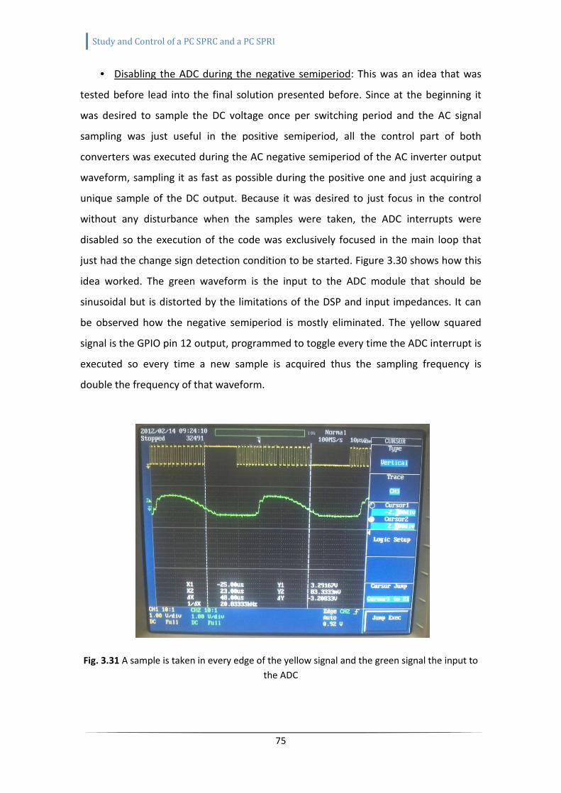
Study and Control of a PC SPRC and a PC SPRI
75
• Disabling the ADC during the negative semiperiod: This was an idea that was
tested before lead into the final solution presented before. Since at the beginning it
was desired to sample the DC voltage once per switching period and the AC signal
sampling was just useful in the positive semiperiod, all the control part of both
converters was executed during the AC negative semiperiod of the AC inverter output
waveform, sampling it as fast as possible during the positive one and just acquiring a
unique sample of the DC output. Because it was desired to just focus in the control
without any disturbance when the samples were taken, the ADC interrupts were
disabled so the execution of the code was exclusively focused in the main loop that
just had the change sign detection condition to be started. Figure 3.30 shows how this
idea worked. The green waveform is the input to the ADC module that should be
sinusoidal but is distorted by the limitations of the DSP and input impedances. It can
be observed how the negative semiperiod is mostly eliminated. The yellow squared
signal is the GPIO pin 12 output, programmed to toggle every time the ADC interrupt is
executed so every time a new sample is acquired thus the sampling frequency is
double the frequency of that waveform.
Fig. 3.31 A sample is taken in every edge of the yellow signal and the green signal the input to
the ADC

Study and Control of a PC SPRC and a PC SPRI
76
In this test, the sampling frequency was set around 400KS/s and can be observed in
the figure above how the ADC interrupts are stopped in the precise moment when the
green signal crosses zero and changes sign from positive to negative. Because all the
control code is executed faster than the duration of the negative semiperiod, the ADC
interrupts are enabled again although the samples are useless. Because this reason,
also the ‘flagT1’ flag was used here to detect that the positive semiperiod has not yet
started.
Disabling the ADC interrupt and even the ADC module during the negative semiperiod
of the AC output signal is a good idea to improve the efficiency of the software.
Moreover, this implementation loses the good advantage of oversampling the DC
output to calculate the mean value and eliminate coupled AC signals since it would not
be really useful to oversample it just in the half period when the inverter output is
sampled due to the loss of the other half. This method was discarded since there were
observed really undesired ripples in the DC output.
• Using a Real Time Operating System (RTOS): A RTOS is an operative system that
has as main objective to concern about the amount of time it takes to accept and
complete a task in a specific deadline. These kind of operating systems offer different
possibilities in terms of scheduling and task managing. Since in the control
software there are two clearly different and independent tasks regarding to the DC
converter output and the AC inverter output controls, the idea of using a RTOS comes
in order to take benefit of a task manager embedded in the operating system being
able to create tasks for every control loop and letting it to manage them in an
equitable way creating a multitask system. The first thought is that a RTOS can be
configured to use a ‘Round-Robin’ scheduling algorithm so it would be a good idea if
the program uses different independent tasks as it happens in this case. Texas
Instruments® offers a RTOS called SYS/BIOS fitted for its DSP devices with an easy-to-
use interface embedded in the CCS® (Code Composer Studio) platform that allows the
programmer to enable and disable all the different subsystems that are going to be
used in the program like semaphores, memory management, scheduling, mutex etc.
When the SYS/BIOS was desired to be tested, the control software had to be reviewed
and some modifications were done to fit the specifications of programing in the RTOS.

Study and Control of a PC SPRC and a PC SPRI
77
First, a template was created with a tool that selects the DSP model and offers some
examples which can be used as a starting base. The main structure of the control
software is almost the same presented before but there is no ADC interrupt since the
DC and AC control tasks wait in their corresponding loops until the flag that warns
about new samples is set. Furthermore, to configure the rest of interrupts in the
SYS/BIOS a .cfg file should be modified. The last different thing, and the main reason of
using this RTOS, is the creation of the DC and AC control loops as independent
functions inside different infinite loops. To execute both processes at the same time,
two tasks are created in the main code and pointed to the control functions adding
some configuration parameters.
Configuring and making the SYS/BIOS work was a tough work since it was the first time
that this RTOS was used by the author and the results were worse than expected. First
of all, the task management programed in this RTOS is not as good as it was expected
at the beginning since there is no ‘Round-Robin’ scheduling algorithm and the
programmer is the one in charge of making the executing distribution of every task so
there is no improvement in using or not the SYS/BIOS to have independent tasks
running at the same time because there is not a real multitasking skill. But the worse
result obtained was in terms of efficiency. Using the SYS/BIOS slowed down the
execution of the software in a noticeable way. This could be proved because even with
the sampling frequency configured as before, the interrupts created by the ADC were
triggered in a much lower rate and they could be observed in the GPIO pin 12 toggling.
Even the use of a RTOS could be useful and offers many possibilities and resources for
really complex programs that share many peripherals, the control software used in
this thesis does not really have a need to use any of these capabilities. The only
interesting block here is the task managing in order to have multitasking but as it was
checked, this is not really good implemented in the SYS/BIOS so the final program
does not include the RTOS.

Study and Control of a PC SPRC and a PC SPRI
78
CHAPTER 4: Hardware implementation
In the previous chapters the resonant converters were introduced, two circuits were
presented as the PC SPRC and PC SPRI and their stability in closed-loop was studied to
design a linear control that maintains their output constant in a range of operation
conditions. In this section the switching circuit with the drivers is introduced as well as
the resonant tank build procedure. Since the resonant tank for the PC SPRC was
already built and totally functional, the description of the elements used is based on
the PC SPRI that has the same resonant configuration. For the switching and drivers
board, a new schematic was designed and built based on the PC SPRC one as the same
switching IGBT module has been used for the AC inverter. The drivers’ board that was
already built for the DC converter was not functional and has been analyzed and
repaired.
4.1. The PC SPRI resonant tank
The schematic of the resonant tank was introduced in chapter 2. It is composed of two
inductors and three capacitors (figure 2.7). To choose the capacitors not only the
capacitance value is important but also the voltage rating. Since for this application
they are working with AC signals the ratings have to be specified accordingly taking
into account that the usual ratings are for DC signals and use to be higher than if AC
signals are used instead. 56nF 1500V capacitors (figure 4.1) are used for the series and
parallel capacitors (Cs and Cp) but because when the phase controlled resonant tank is
built the value of the output parallel capacitor is 2Cp, two 56nF are placed in parallel to
obtain a 112nF capacitance that provides the AC output between its terminals.

Study and Control of a PC SPRC and a PC SPRI
79
Fig. 4.1 Capacitor used for the PC SPRI resonant tank
By the other hand, the inductors were hand-made built using a specifically selected
core and copper wire. To design and build an inductor some constraints have to be
taken into account, these are the non-saturation of the core, that is related with the
maximum current that flows through the inductor and the number of turns of copper
wire over the core, and the inductor value, that can be tuned also with the number of
wire turns and with the length of the gap between the two parts of the core. The first
condition that must be accomplished is formulated in equation (4.1) where N is the
wire turns over the core, L is the desired inductance value, IMAX is the maximum
current through the inductor and S and BSAT are parameters given by the core
manufacturer that stand for the section [m2] and magnetic flux density [Tesla].
≥ ·q6$·3n (4.1)
To determine the number of turns needed to build the inductor desired value, a
relation between an electric circuit and a magnetic circuit is applied. The idea is to use
the same fundamentals that describe Ohm and Kirchhoff laws but substituting the
electric parameters by the magnetic ones, using flux instead of current and reluctance
instead of resistance, thus a magnetic core can be described by the magnetic circuit
shown in figure 4.2 where the wire copper is turned over the middle legs of two E
cores coupled together creating an electromagnetic excitation Ni with a flux response
Φ that is related to the reluctances R.

Study and Control of a PC SPRC and a PC SPRI
80
Fig. 4.2 Equivalent magnetic circuit of an E core
The reluctance can be expressed in terms of section, longitude and magnetic
permeability as shown in equation (4.2)
ℛ = c·: (4.2)
All parameters to calculate the reluctance are provided by the datasheet of the chosen
core. In this specific case an E core is used to build both inductors of the resonant tank
with the specifications listed below:
• A1= 196.35mm2
• A2= 361.2mm2
• S (Ae)= 353mm2
• l1= 46mm
• l2= 23.425mm
• Permeability (µ)= 2500 H/m (±25%)
• Saturation magnetic flux (Bsat)= 0.5T
• Material: Ferrite
• Material Grade: P
The equivalent reluctance of the E core magnetic circuit can be expressed as (4.3)
ℛ =ℛ# + 2ℛ + ℛ + ℛ' (4.3)
Applying Faraday’s law relating number of turns with flux (4.4), taking the equation of
voltage of an inductor (4.5) and the equivalent Ohm’s law for magnetic circuits (4.6)
one can lead to equation 4.7 that relates the number of turns necessary to create an
inductance of value L with an equivalent reluctance of the core R.

Study and Control of a PC SPRC and a PC SPRI
81
_ = · oL (4.4)
_ = ` · L (4.5)
= ℛ · Φ (4.6)
` = %ℛ (4.7)
Because using just the characteristics of the core can lead to a number of turns that
don’t accomplish the inequation (4.1), there is the possibility to add a little air gap or
space between the two E magnetic cores modifying the total reluctance value thus the
number of turns of wire for the same value of inductance. This reluctance created by
the air gap is represented in figure 4.2 as R.3 and its value is calculated with equation
(4.2) using as length the space between cores (usually from tenths of millimeters to a
few millimeters) and the air permeability µ0. Since the total reluctance increases, it can
be probed from equation (4.7) that the number of turns to keep the same inductance
have to increase thus inequation (4.1) can be accomplished easily.
Using the specifications of the core listed before and knowing by simulations that the
maximum current through the tank is three amperes, for an inductance of 2.55mH the
minimum number of turns (4.1) are N=43.34=44. By using (4.2) and (4.7) the specific
turns needed without airgap are N=17.29=18 so it does not accomplish the previous
constraint. A 0.426mm air gap is added between the two E cores increasing the total
reluctance and finally having a total number of copper wire turns over the cores of
N=50 that widely accomplishes the minimum so a security range is created in case the
current increases unexpectedly. Figure 4.3 illustrates the inductor building process
where four E cores are used to build the two inductors with copper wire turned over a
plastic bobbin, a finished inductor is also shown in the same picture. The airgap
between the two E cores is created using pieces of paper and sealing the perimeter of
the core with electric tape. As the paper permeability might differ from the air one, the
gap is tuned measuring the total inductance with a specific device until the desired
value is achieved.
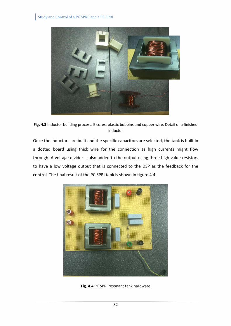
Study and Control of a PC SPRC and a PC SPRI
82
Fig. 4.3 Inductor building process. E cores, plastic bobbins and copper wire. Detail of a finished
inductor
Once the inductors are built and the specific capacitors are selected, the tank is built in
a dotted board using thick wire for the connection as high currents might flow
through. A voltage divider is also added to the output using three high value resistors
to have a low voltage output that is connected to the DSP as the feedback for the
control. The final result of the PC SPRI tank is shown in figure 4.4.
Fig. 4.4 PC SPRI resonant tank hardware

Study and Control of a PC SPRC and a PC SPRI
83
4.2. The PC SPRI Control board
The control board of both the PC SPRC and PC SPRI is composed by different sections.
The main part of the board is the four switches that create the resonant tank input
squared signal using the voltage input source. Because these switches work with high
currents and voltages and the control signals are provided by a digital device and
because of different voltage references, isolation is required between the control
signal and the input to the drivers that control the switches. Isolation is also required
to close the loop from the high voltage output to the input of the ADC module of the
DSP. The last section of the control board is the different voltage regulators and DC-DC
low voltage converters that provide all the different needed voltages to supply the
devices. Figure 4.5 schematizes the diverse sections of the PC SPRI where the blue
modules are the ones built in the control board. It can be ascertained how the DSP is
isolated from the input and output signals from the rest of the system.
Fig. 4.5 PC SPRI modules schematic. Control board modules are marked in blue
Although the PC SPRC control board including the regulators, switches and isolation
was already built some years ago, the whole circuit had to be studied and repaired
since some wires were broken and was not clear where they should be connected and
the feedback isolation part was burned and not clearly designed. The control board of
the PC SPRI is based in the PC SPRC one since the used switching module model is the
same, but has been enhanced and some components have been changed as they were
out of date and no longer sold. The PC SPRC control board needs three different

Study and Control of a PC SPRC and a PC SPRI
84
supply voltages (+20V, +15V and -15V) thus at least two different power supplies have
been used to power the circuit. For the new control board, just a ±20V supply is
needed and it can be powered with just one power supply.
The schematics of the control board circuit can be found in appendix IV and appendix V
where the first circuit represents the control signals isolation and the switching
module and the second one the voltage supply module and the feedback isolation. In
the next sections, all different modules are explained but not in an extensive manner.
For more details see the corresponding datasheets of each used device. It is also
recommended to check the schematics in the appendix to follow the circuit diagram.
4.2.1. Switches and drivers
The switches and drivers are embedded in a module (Mitsubishi® PM30CSJ060) where
four high power IGBT’s with antiparallel diodes are connected in a full bridge
configuration and are controlled by a low voltage signal. The module also includes over
current, over temperature and under voltage protections. It is suited to work at
switching frequencies up to 20KHz and the IGBT’s can handle currents until 30A and
collector-emitter voltages up to 600V. The diagram of the IGBT’s and drivers module
can be found in appendix VI. Because the input switching in the PC SPRC and PC SPRI
work in the same manner and the PM30CSJ060 IGBT module was used in the PC SPRC
with a proper operation, it is also used in the inverter.
4.2.2. Control signals isolation
The control signals are provided by the PWM module of the DSP. These are digital
signals that are used to control each of the IGBTs inside the PM30CSJ060 module.
Since the control of the transistors is done applying a signal over a voltage threshold
between their base and emitter pins and all four DSP signals are referred to ground,
isolation is required between the control signals and the input to the base-emitter pins
so the control signals can be referred to every different IGBT emitter. Optocouplers
(A4504) devices are used for this purpose but they have to be supplied by isolated
voltages with different grounds so every output has its own ground that as it is
explained in the previous lines is the emitter of every IGBT. By the other hand the
optocouplers provide an inverse output, but this is solved using active high control

Study and Control of a PC SPRC and a PC SPRI
85
signals from the DSP as the IGBTs module requires active low ones. A voltage follower
is built using an operational amplifier chip (TLE2144) powered with 5V provided by the
DSP board and placed between the output of the DSP and the optocouplers so the
input load does not modify the shape of the signal. By using optocouplers, the DSP
remains isolated from the power switching device and also the control signals are
applied properly between the pertinent pins in every IGBT.
4.2.3. Feedback isolation
The main purpose of the feedback isolation is to separate analog components from the
digital ones. Although the output of the PC SPRI is stepped down by a high impedance
resistor network, is always recommended to separate the digital control device from
the plant. In the case of the PC SPRC the feedback isolation is also used because the
output is not referred to the same ground as the DSP is, so grounds must be separated.
In both cases an isolation amplifier is used (ISO124P) and as it needs to be supplied by
two independent power sources with V=±15V, a low voltage DC-DC converter
(DCP011515) is used to provide the required voltage at the isolated side of the
amplifier.
4.2.4. Voltage supply module
Since all modules need to be powered, there are also some different voltage
requirements and different ground references are necessary, some chips have been
selected creating the voltage supply module. Everything in the control board is
powered by an external supply of ±20V as this is the maximum voltage needed by the
DC-DC converters (NDY2415C) that have an output of 15V referred to a floating
independent ground and power every IGBT driver with the corresponding optocoupler.
Also a floating ±15V supply is needed to power the isolated side of the isolation
amplifier (±Vs2 from figure 4.6). A DC-DC converter (DCP011515) is used, as it was said
before, to provide this voltage. Since the supply for this low voltage converter and for
the ±Vs1 pins of the isolation amplifier (figure 4.6) are ±15V and it was desired to just
power every chip with a unique ±20V, two voltage references (MC7815C and
MC7915C) are also placed in the board to provide +15V from the +20V and -15V from
the -20V respectively.

Study and Control of a PC SPRC and a PC SPRI
86
Fig. 4.6 Schematic of an isolation amplifier used in the feedback isolation
The built control board is pictured in figure 4.7 where the analog connections are done
using banana connectors and all the digital inputs and output are done using pins. An
important point to be considered is the connection between the stepped down output
voltage of the PC SPRC and the isolation amplifier. As this signal is a DC voltage, some
undesired AC couplings may occur and interfere in a very bad way in the control
closed-loop. To avoid this, a twisted short wire should be used between the resistor
net output and the isolation amplifier input. In the case of the PC SPRI may be also
useful to avoid other undesired EMI but since the main interference in the system
comes from the 20KHz switching and the output of the inverter is exactly the same
frequency, the interference, if produced, is not noticed.

Study and Control of a PC SPRC and a PC SPRI
87
Fig. 4.7 The control board
The banana connections observed in the top side of the control board of figure 4.7 are
the input from the high voltage supply and the two outputs to the tank. The right edge
blue screw connectors are the output from the stepped-down voltage from the tank
and the input to the ADC inverter channel (A1). The four screw connectors on the
lower edge are the external supply voltages (-20V, GND and +20V). And finally the
vertical array of pins in the middle section of the board are the ones used to connect
the PWM control signals from the corresponding GPIO pins and the 5V and GND all
provided by the DSP board. These pin connections are detailed in figure 4.8.
Fig. 4.8 Pin connections in the control board

Study and Control of a PC SPRC and a PC SPRI
88
CHAPTER 5: Experimental results
5.1. Overview of the performed experiments
After introducing the circuit of the DC-DC converter and the DC-AC inverter, study the
stability, design and implement a controller, performing the simulations and build or
repairing the circuits, the experimental results are shown in this chapter. At a first
instance and while the project was being developed, a low voltage version was built
using a specific voltage divider doing the regulation of the PC SPRC at an output
voltage of V=11V and the PC SPRI one at V=11.5V. These tests were performed with
load and without and after tuning the PI control constants for both circuits and
performing some successful experiments, the high voltage version was built changing
the voltage dividers that connect both outputs of the resonant converters to the inputs
of the ADC. Since the operation point of the ADC is at the middle of its voltage range,
that goes from 0V to 3V, and represents a voltage reference of Vref=1.5V, the voltage
divider of the PC SPRC is designed to have a gain of α=1.5/300=0.005. This is built with
high value resistors so the minimum power is lost in this stepping down and the 300V
output connected with the 1:100 transformer gives the 30KV of DC desired voltage.
The same procedure is used for the PC SPRI, a divider of gain
α=1.5*sqrt(2)/200=0.0106066 is built so an output of V=200Vp connected to a 1:50
transformer provides a 10KVp AC voltage. Actually, for the high voltage tests the
transformers have not been used. Although the components of the output DC filter
were purchased, the experimental laboratory where the project was designed was not
found suitable, as long as security measures refer, to perform such high voltage
experiments. Even though, the 1:100 transformer with the low voltage PC SPRC version
was tested with success, having a 1.1KV output measured with two stepped voltage
dividers.
To perform the high voltage version experiments, high power rated resistors are used
to load both circuits. As the load operation point the system was designed for is 1MΩ,
the equivalent resistance in the primary side of the DC converter is RL=100Ω. A 200W,
100Ω ceramic power resistor is used (figure 5.1). Moreover, the 300V operation point
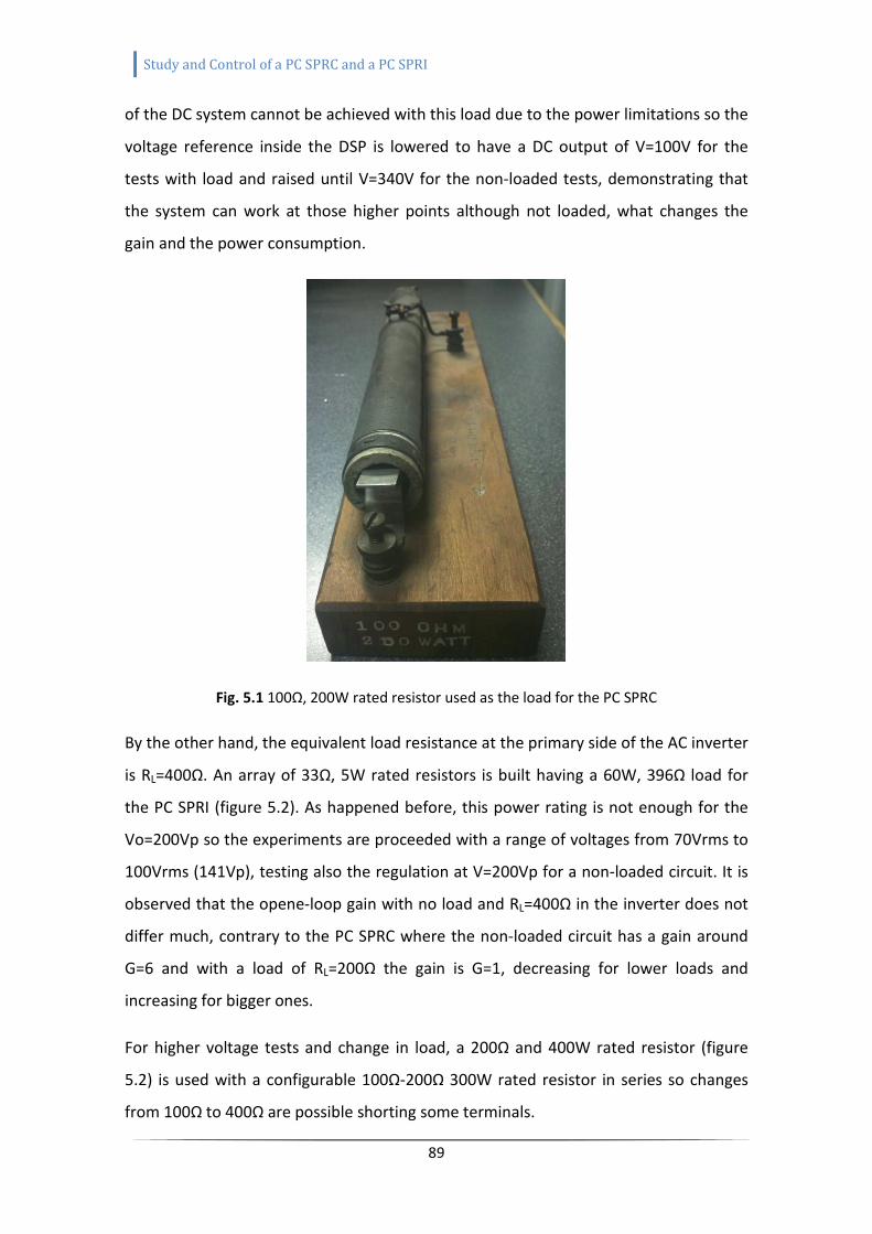
Study and Control of a PC SPRC and a PC SPRI
89
of the DC system cannot be achieved with this load due to the power limitations so the
voltage reference inside the DSP is lowered to have a DC output of V=100V for the
tests with load and raised until V=340V for the non-loaded tests, demonstrating that
the system can work at those higher points although not loaded, what changes the
gain and the power consumption.
Fig. 5.1 100Ω, 200W rated resistor used as the load for the PC SPRC
By the other hand, the equivalent load resistance at the primary side of the AC inverter
is RL=400Ω. An array of 33Ω, 5W rated resistors is built having a 60W, 396Ω load for
the PC SPRI (figure 5.2). As happened before, this power rating is not enough for the
Vo=200Vp so the experiments are proceeded with a range of voltages from 70Vrms to
100Vrms (141Vp), testing also the regulation at V=200Vp for a non-loaded circuit. It is
observed that the opene-loop gain with no load and RL=400Ω in the inverter does not
differ much, contrary to the PC SPRC where the non-loaded circuit has a gain around
G=6 and with a load of RL=200Ω the gain is G=1, decreasing for lower loads and
increasing for bigger ones.
For higher voltage tests and change in load, a 200Ω and 400W rated resistor (figure
5.2) is used with a configurable 100Ω-200Ω 300W rated resistor in series so changes
from 100Ω to 400Ω are possible shorting some terminals.

Study and Control of a PC SPRC and a PC SPRI
90
Fig. 5.2 Up: 396Ω, 60W rated resistor used as the load for the PC SPRI. Down: 200Ω 400W
resistor used to test the change of load
Once the operation points are set in a safe region for the loads changing the reference
value, and having succeeded with the non-loaded experiments so the converter and
inverter work as expected, the control is put under test and some experiments are
performed to see its response. These experiments are based on load changes and
reference value changes. Since the input voltage is manually tuned with a knob and
there is no possibility to program a step via GPIB port in the high voltage power supply,
the response of the input voltage change is visually checked, meaning that the knob is
tuned while observing a permanent output voltage value. For the low voltage version,
this test was successfully performed and shown in the first figures.
Is very important to notify that the DC high voltage supply used for the experiments
offers a big rectified ripple at the output and this is what gets inside the system under
test. This ripple affects the output in a minor way that is presented in the input as is a
low frequency signal (60Hz from the grid) and the control tries to get rid of it, but some
figures, specially the PC SPRC output, present disturbances that should not be there

Study and Control of a PC SPRC and a PC SPRI
91
but are caused by this fact although, to improve the input voltage to the system, a big
capacitance is connected in parallel with the supply acting as a filter of the undesired
disturbances as it is shown in figure 5.3, where the high voltage power supply is
attached to the electrolytic capacitor. Figure 5.4 shows the experimental bench with
the six boards used (SPRC tank, SPRI tank, PC SPRC control board, PC SPRI control
board, DC converter feedback isolation board and the DSP), the laptop where the
software is developed and programmed into the DSP, the loads and the power sources
(two power sources are used to power the boards with ±20V and ±15V also needed for
the DC control board). To take the measures, an oscilloscope is used at first instance
but isolation is needed to observe the PC SPRC output as it comes from a rectifier and
the ground is not the same as the scope so a floating scope is used instead for almost
all the measurements. A Fluke® floating advanced multimeter with an included scope
is used to observe the signals from the system. As far as the experiments that are
taken in this thesis, this device is widely enough.
Fig. 5.3 Input high voltage power supply with a parallel high capacitance to improve the output
big ripple

Study and Control of a PC SPRC and a PC SPRI
92
Fig. 5.4 The testing bench. Up left: Detail of the six boards: The upper one is the PC SPRI tank,
the one in the middle is its control board, on its left is the PC SPRC control board, the one on
the bottom-left corner is the PC SPRC tank, right next to it the feedback isolation and the green
board is the DSP. Bottom left: Measurements with a floating scope. Right: View of the overall
tested system with the programming laptop.
5.2. The low voltage version
The PC SPRC and PC SPRI low voltage versions are designed and tested just to
determine a good circuit response with no overvoltage risk. A response of a voltage
variation in a low voltage input source is shown for the DC converter that takes 3ms to
establish the steady voltage again. It is also good to observe in the next figure the
steady state at 20KHz and 16Vp for the PC SPRI.

Study and Control of a PC SPRC and a PC SPRI
93
5.2.1. The PC SPRC response
Fig. 5.5 Response of the PC SPRC low voltage version to a change in the input
5.2.2. The PC SPRI steady state
Fig. 5.6 PC SPRI low version regulated steady state

Study and Control of a PC SPRC and a PC SPRI
94
5.3. The high voltage version
For the real operation point experiments, the voltage divider (or closed-loop gain) is
changed in order to have a 300V DC and 200Vp AC outputs. By the other hand, a
limitation is imposed by the power rating of the loads used in the experiments.
Although special power resistors are used, the 900W needed for the PC SPRC are far
from the available loads so the digital voltage reference of the DSP is lowered
performing the tests between 100V and 170V instead of the 300V-350V. In the case of
the inverter, the limitation is not the load but the input power supply that can only
bring up to 170V. This is enough if the load is the nominal RL= 400Ω where a gain a bit
above one can reach the steady state. If the load is lowered the gain decreases and the
output drops down being out of the control range. In the load variation tests, the
voltage reference is decreased to V=120Vrms or V=170Vp.
5.3.1. The PC SPRC response
For the DC converter, the operation point is shown in figure 5.7, with a regulated
output at 343V in a non-loaded state. Figure 5.8 represents the 20Khz and 1.5Vp ripple
at the output when a regulation is performed around 150V. This ripple is coupled to
another low frequency ripple from the input power supply. The output 20KHz filter is
considered good enough as the ripple value is 1.06Vrms what means less than 1% of
the DC output value. Figure 5.9 represents the efficiency calculation. Because of the
bad quality of the input voltage, this result might not be the correct one but the
efficiency is calculated as (5.1) with RL=100Ω, Vi=50V, Ii=0.479A and Vo=41.7V what
yields η= 72.6%.
= hO∗qO%j
(5.1)
The changes in the load and in the voltage reference show that the control works in a
good manner with the tuned proportional and integral constants with responses that
go from 3ms to 7ms. The final PI constant values are Ki/fs=0.075 and Kp=0.025

Study and Control of a PC SPRC and a PC SPRI
95
Fig. 5.7 Steady state regulated operation point for the PC SPRC without load
Fig. 5.8 Switching frequency ripple at the PC SPRC output with an operation regulated point of
150V

Study and Control of a PC SPRC and a PC SPRI
96
Fig. 5.9 Demonstration of the efficiency calculation in the PC SPRC
5.3.1.1. Load change
Fig. 5.10 PC SPRC output response to a change in the load from 400Ω to 200Ω with regulation
at 170V

Study and Control of a PC SPRC and a PC SPRI
97
Fig. 5.11 PC SPRC output response to a change in the load from 200Ω to 400Ω with regulation
at 100V
5.3.1.2. Voltage reference change
Fig. 5.12 Change in the voltage reference from an output regulation of 100V to 170V

Study and Control of a PC SPRC and a PC SPRI
98
5.3.2. The PC SPRI response
The same procedure as before is followed to test the inverter. First a no loaded output
at the 200Vp operation point is shown in figure 5.13. Figure 5.14 shows the procedure
to calculate the efficiency using equation (5.1) with Vi=50V, Ii=0.198A, RL=400Ω and
Vo=57.5Vrms yielding an efficiency of η=83.5%.
The load and reference variations show a fast response of the control with just a 500us
transitory in all cases, concluding that the PI constants are well tuned. Some other
experiments are performed varying these constants but the final values are set to
Ki/fs=0.7 and Kp=0.3
Fig. 5.13 PC SPRI operation point regulated at Vo=200Vp

Study and Control of a PC SPRC and a PC SPRI
99
Fig. 5.14 Demonstration of the efficiency calculation in the PC SPRI
5.3.2.1. Load change
Fig. 5.15 PC SPRI output response to a change in the load from 400Ω to 200Ω with regulation
at 170Vp

Study and Control of a PC SPRC and a PC SPRI
100
Fig. 5.16 PC SPRC output response to a change in the load from 200Ω to 400Ω with regulation
at 170Vp
5.3.2.2. Voltage reference change
Fig. 5.17 Change in the voltage reference from an output regulation of 170Vp to 220Vp with a
400Ω load

Study and Control of a PC SPRC and a PC SPRI
101
CHAPTER 6: Conclusions
This thesis demonstrates how a Phase-Controlled Series-Resonant Converter and a
Phase-Controlled Series-Resonant Inverter can work at high voltages being controlled
with the same DSP device using linear conventional methods resulting in a fast
response even for changes in the input voltage power supply or in the output load.
Along all the project, a PC SPRC tank and its control board have been refurbished and
the dissertation of their design has been followed in a parallel work to design the PC
SPRI tank where its control board is based in the same switching module as the PC
SPRC one but has been enhanced to be powered with just one positive-negative
voltage. The Texas Instruments® TMS320F28335 DSP has been deeply studied to
implement a PI control based on a phase shifting of the switches control signals from
the full-bridge design in both converters. This control is derived from the stability study
in closed-loop of the PC SPRC and PC SPRI and deeply tested all over the
implementation of this project. The high-order models of both plants are resulting
from a previous PhD work for the PC SPRC and the same method has been used to
obtain the PC SPRI one. This last plant has been tried to reduce using gramian
techniques resulting in a non-reductible high-order transfer function. Some Matlab®
programs have been written to automatically obtain bode plots and root locus from all
the blocks of the closed-loop system. A non-tested spark control has been also
programmed. The operation point set for both converters meets the specifications for
an electrostatic precipitator application. Several experiments have been worked out to
demonstrate, basically, the good response of the designed and implemented control.
The major contributions along this thesis are:
• Study and understanding about resonant power converters and contribution to
the design of a PC SPRI.
• Stability study and design of the closed-loop control of a PC SPRC.
• Stability study and design of the closed-loop control of a PC SPRI.
• Implementation of both controllers in the Texas Instruments® TMS320F28335
DSP. A detailed explanation of the software is presented.

Study and Control of a PC SPRC and a PC SPRI
102
• Implementation of a spark control in case of a bridge-short-circuited output.
• Implementation and testing of different methods to improve the digital control
(use of a RTOS…).
• Design and implementation of a control board for the PC SPRI based on an
improvement of the one used to control the PC SPRC. This last one needs two
positive-negative voltage sources while the designed one needs just one.
• Matlab® automation programs for the transfer function calculations and
Simulink / PSpice® simulations.
• Practical experiments of both the PC SPRC and PC SPRI are performed and
shown.
• Although the high voltage transformers have not been used in the specified
operation point, an equivalent load at the primary has been used in the
experiments to demonstrate the reliability of both systems to work in an
electrostatic precipitator application.
6.1. Future works
Although an idea of a spark control is implemented in the DSP software and a current
sensor has been purchased to fit this objective, it has not been tuned for its correct
operation as the high voltage transformers have not been used since the security
measures were not considered enough for those experiments. Experimentation on a
high voltage suited area is desired to connect the transformers and check the real
output of the system.

Study and Control of a PC SPRC and a PC SPRI
103
APPENDIX I
TABLE 1: Inverter resonant tank element values
Ls (mH) Cs (nF) 2Cp (nF) ESR (Ω) RL F res
(KHz)
F swit
(KHz)
2.55 56 112 5 400 19 20
TABLE 2: DC-DC converter resonant tank and filter element values
Ls (mH) Cs (nF) 2Cp (nF) ESR (Ω) RL F res
(KHz)
F swit
(KHz)
1.22 100 220 5 100 19 20
Lf (mH) Cf (uF)
5.47 4

Study and Control of a PC SPRC and a PC SPRI
104
APPENDIX II
Full bridge phase controller Matlab® Simulink Schematic

Study and Control of a PC SPRC and a PC SPRI
105
APPENDIX III
Control Board schematic: IGBT module and ctrl signal isolation

Study and Control of a PC SPRC and a PC SPRI
106
APPENDIX IV
Control Board schematic: Voltage supply and feedback isolation

Study and Control of a PC SPRC and a PC SPRI
107
APPENDIX V
IGBT Mitsubishi® PM30CSJ060 module internal schematic:

Study and Control of a PC SPRC and a PC SPRI
108
APPENDIX VI
PC SPRC closed-loop Matlab® Simulink simulation schematic

Study and Control of a PC SPRC and a PC SPRI
109
APPENDIX VII
PC SPRI closed-loop Matlab® Simulink simulation schematic
Study and Control of a PC SPRC and a PC SPRI
110
Bibliography
[1] D. Czarkowski and M. K. Kazimierczuk “Phase-controlled series-parallel resonant
converter”, IEEE Transactions on Power Electronics, Vol.8, Nº 3, pp. 309-319,
July 1993.
[2] D. Czarkowski and M. K. Kazimierczuk “Resonant power converters” John Wiley
& Sons, Second Edition, 2011.
[3] R. W. Erickson and D. Maksimovic “Fundamentals of Power Electronics”, Kluwer
Academic Publishers, 2nd
Edition, 2001. Chapter 19.
[4] M. Rokvick “Modeling and design of a Phase-Controlled Series-Parallel resonant
Inverter” Power Electronics Master’s Thesys, 2012, Poly-NYU.
[5] S. Zheng “Modeling and control of voltage-fed Phase-Controlled Resonant
Converters” Power Electronics PhD Dissertation, 2003, Poly-NYU.
[6] M. Rashid “Power electronics Handbook”, Butterworth-Heinemann, 3rd
Edition,
2010.
[7] Texas Instruments® “TMS320F28335, TMS320F28334, TMS320F28332,
TMS320F28235, TMS320F28234, TMS320F28232 Digital Signal Controllers
(DSCs)” Data Manual, Literature Number: SPRS439I, June 2007–Rrevised
March 2011.
[8] Texas Instruments® “TMS320x2833x Analog-to-Digital Converter (ADC)
Module”, Reference Guide. Literature Number: SPRU812A, September 2007–
Revised October 2007.
[9] Texas Instruments® “TMS320x2834x Delfino Enhanced Pulse Width Modulator
(ePWM) Module”, Reference Guide. Literature Number: SPRUFZ6B, March
2009–Revised September 2009.
[10] Texas Instruments® “TMS320x2833x, 2823x System Control and Interrupts”,
Reference Guide. Literature Number: SPRUFB0D, September 2007–Revised
March 2010.
[11] Texas Instruments® “TMS320x28xx, 28xxx DSP Peripheral”, Reference Guide.
Literature Number: SPRUFB0D. September 2007–Revised March 2010.

Study and Control of a PC SPRC and a PC SPRI
111
[12] Y-K Lo, C-Y Lin, M-T Hsieh and C-Y Lin “Phase-Shifted Full-Bridge Series-
Resonant DC-DC Converters for Wide Load Variations” IEEE Transactions ons
Industrial Electronics, Vol.58, Nº 6, June 2011.
[13] E. Pinheiro, O. Postolache and P. Girao “Digital notch filters implementation
with fixed-point arithmetic” XIX IMEKO World Congress, September 2009.
[14] J.A Martin Ramos, A.M Pería, J. Díaz, F. Nuño, J.A. Martínez “Power supply
for a High-Voltage Application” IEEE Transactions on power electronics, Vol.
23, Nº4, July 2008.
[15] J.A Martin Ramos, A.M Pería, J. Díaz, F. Nuño, J.A. Martínez “Dynamic and
Steady-State Models for the PRC-LCC Resonant Topology With a Capacitor as
Output Filter” IEEE Transactions on industrial electronics, Vol. 54, Nº4,
August 2007.
[16] B. Yang “Topology investigation of front end DC/DC converter for distributed
power system”, Electrical and Computer Engineering PhD Dissertation, 2003.
VirginiaTech.
[17] R. M. Murray, Z. Li and S. S. Sastry, “A Mathematical Introduction to Robotic
Manipulation”, CRC Press, 1993.