marconi instrumentation - american radio history ... · vol. 8 no.8 december, 1962 marconi...
TRANSCRIPT

VOL. 8 NO. 8 DECEMBER, 1962
MARCONI
INSTRUMENTATION A Technical Information Bulletin
Issued Quarterly by
Marconi Instruments Limited, St. Albans, England
IN THIS ISSUE
SEEING IS BELIEVING page 169
OSCILLOSCOPE, TYPE TF 2200.. 171
A 1% SENSITIVE VALVE VOLTMETER .. 192
INDEX TO VOLUME EIGHT 198
ELECTRONIC INSTRUMENTS FOR TELECOMMUNICATIONS AND INDUSTRY

e
,iri r r.2:4, -- e
i _; ,..___
1.,.''t ,;177,7,_:,,,,, b" '''''' ' -'-' .-. '," -ie ..,
..' ' ij ii :: r , .- .% 1;"' .e7, I if. ..7_,..
-.bi "t:- t-2.-rt"
ih -,.7,:''' r
.---j.,, . f", . ,...o_f_oX -... .,-j. _,, _ .
-7..-., - -, 7,..x,,,,, i
.:, 3,;, .. ' .r». -f--.: . ; . , -,,,11Lil 2, ' . 1 - , ,,
';' .2 ' j"-;',. .i ...ffleor....,'3.:'', - -2.:-.. Sr I > . I - 2
''d,',e 'i - = :- 7 4 '-'2' ----_.11:ai'm -. ei --1, , , - e- _i -,
'-iii ' -P1 1 .i. .:Ir ,... 4 .;.-1 i'n' 1,_1," - , rii.- 11,- c427'; '
r.ii , ,ffir
t .
el ,..r =-_, ' -4". - ..--7.,4*-:_, lekt,w1.,._:._7: , ..=,, , j, z.-. _.
A _
r et:5-1 cle-e"'4
_- -

o
VOL. 8 NO. 8
DECEMBER, 1962
Issued with
the compliments of
MARCONI INSTRUMENTS
LIMITED
ST. ALBANS
ENGLAND
EDITORS
P. M. RATCLIFFE, A.M.I.E.E.
and
J. R. HAYWARD, A.M.Brit.I.R.E.
The copyright of all articles is strictly reserved but the material may be reprinted without permission providing definite acknowledgement is made to Marconi Instruments Limited.
169
MARCONI INSTRUMENTATION
Seeing is believing DUE TO THE inconveniently small dimensions of the electron, circuit performance can only be interpreted by the judicious use of measuring instruments requiring both skill and experience in their application and an understanding of the information presented. There are, of course, exceptions to this, as with all sweeping generalizations, but in electrical engineering these exceptions are normally indicative of catastrophic failure rather than normal circuit operation, and can be detected without recourse to serious measurements. Of necessity, the majority of instruments that are available for laboratory and field use are purpose built to indicate one particular aspect of circuit behaviour. Generally the result is displayed as a numerical quantity either on a dial, a meter, or to use the latest technique, as a true digital read-out. Consider quite an elementary operation-that of measuring the parameters of a sinusoidal waveform such as frequency, amplitude and distortion. For maximum accuracy the choice would be an electronic counter, a valve voltmeter, and a wave analyser or distortion factor meter capable of measuring the harmonic and hum content. With this trio it would be possible to define the waveform exactly. But this is considering only the simplest case. As the waveform becomes progressively more complex, so the validity of the results becomes more dubious, and greater caution is required in ensuring that the particular apparatus employed is being operated within its capabilities. In the limit, it is essential to see the waveform to acquire a true appreciation of the circuit operation.
An entirely different approach to this problem of examining a waveform is offered by the oscilloscope. This and kindred devices, which utilize the cathode ray tube as their method of display, are unique among electronic instruments as they provide an immediate representation of electrical occurrences in a visual form; the time between cause and effect approaches zero, being determined only by the electron velocity on its journey to the tube phosphor. The real elegance of an oscilloscope is in its ability to display simultaneously all the various parameters of any waveform, whereas formerly each required an individual purpose built instrument. Now as the waveform becomes more complex, so the instrument becomes more useful, and is essential if any work is to be conducted on circuits involving pulse techniques such as are found in computers and television systems. It is perhaps to television entertain- ment that the oscilloscope owes its present notoriety. Not only can a c.r.t. be found occupying pride of place in nearly every home, but the oscilloscope itself is often displayed on the screen of that c.r.t. whèn it is desired to create an atmosphere of great scientific endeavour.
It should also be remembered that the activities of the general purpose oscilloscope are not confined exclusively to the field of electronics. Any physical quantity that can, with the aid of a suitable transducer, be converted into a voltage, can be applied to the plates of an oscilloscope for visual examination. This allows many non -electrical phenomena also to be analysed. A search through current literature shows that there are applications in such diverse industries as coal -mining, aircraft, machine tool, plastics and transport, in addition to the various medical requirements.
Although Marconi Instruments have, for many years, used the c.r.t. as a component in various designs, it was not until three years ago that the growth of the Company was sufficient to spare the engineering and production effort to enter the truly general

170 MARCONI INSTRUMENTATION VOL. 8 NO. 8
Trafalgar Square-where a copy of the Standard Yard, which is the ultimate reference for length, can be readily referred to.
For determining wave -length and amplitude of recurrent electrical signals, however, electronic engineers are more likely to turn to a measuring oscilloscope such as the TF 2200 described on page 171
purpose oscilloscope field with the type TF 1330. This was announced in the June 1959 issue of this journal; with a promise of more to come in the future. Towards the end of the same year a dual trace version, namely the TF 1331, also became available. Both these instruments have similar specifications, the important parameters being a bandwidth of d.c. to 15 Mc/s, giving a rise time of 25 nsec, and a sensitivity of 50 mV/cm. During the intervening years slightly modified versions of these have been produced to satisfy particular needs, as well as a number of accessories. The last of these was the Delay Generator Type TF 1415 which was introduced this year in the March issue. The success of our first venture into pastures new has encouraged us to take the next logical step forward with designs in this category, and the majority of this issue is devoted to a description of the oscilloscope Type TF 2200. This, in itself, is a departure from our normal practice, as we usually present several topics so that there is something of interest for all, but knowing that modern oscilloscope techniques concern every electronic engineer a very detailed article is pre-
sented here. To try to demonstrate the finer points of handleability a double -page coloured photograph has been included, which also shows the latest Marconi Instruments approach to industrial design.
One of the major problems which confronted the development team at the outset of this project was the definition of the term `general purpose'. As the band- width increases so does the number of possible appli- cations, until the desired performance specification could transform the mechanical design from the portable class to the almost immovable. This problem of size has been solved by a series of plug-in Y -deflection units, herein- after referred to in oscilloscope parlance as `plug -ins'. A dual advantage is offered by this approach as it not only restricts the weight but allows the customer to purchase those units for which he has an immediate need. As a by-product of this necessity, there is the further advan- tage that new plug -ins can be designed as and when new requirements arise, thereby increasing its versatility as a general-purpose device through which circuit perform- ance can be seen and hence believed. P. M. R.

MARCONI INSTRUMENTS
NEW
DESIGN
Oscilloscope
by J. D. MIDDLETON, Graduate I.E.E.
171
621.317.75
TYPE TF 2200
A 35 Mc/s general purpose measuring oscilloscope designed with specific features for use in television waveform measurements. A range of plug-in Y' pre-amplers extend its versatility whilst a delaying time base with comprehensive triggering facilities enables precise measurements to be made on even the most complex of waveforms. Every effort has been made to reduce the number of preset controls and to make the
oscilloscope simple to use without sacrificing any of the facilities expected of such an
instrument. The elimination of both the `Stability' control and the need for front panel links are two examples of this. Centimetre graticule and slide -back measurements can be made both in voltage and time
depending on the accuracy required and graticule calibration can be checked without disconnecting the input signal.
THE TF 2200 is a laboratory measuring oscilloscope with a bandwidth up to at least 35 Mc/s, a rise time of 12 nsec and a sensitivity of 50 mV/cm. A full 5 cm display is available throughout the frequency range and the 10 kV post -deflection accelerating potential ensures adequate brilliance with writing speeds up to 10 nsec/cm. Time and voltage measurements are made by slide -back techniques or centimetre graticule, and delayed sweep facilities enable any portion of a complex waveform to be dis- played.
Versatility is increased by a range of `Y' -amplifier plug -ins: a Single -Trace Unit with a pass -band of d.c. to 38 Mc/s, or d.c. to 30 Mc/s with Gaussian roll -off; a Dual -Trace Unit using electronic beam switching; and a
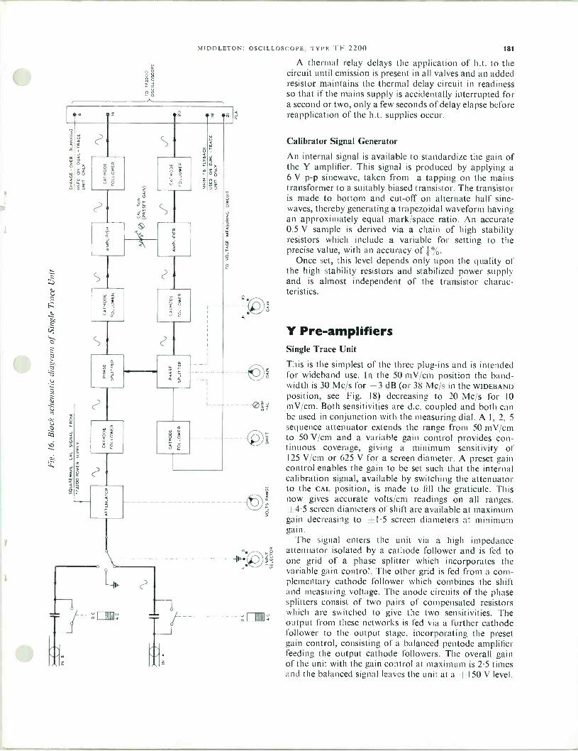
Fig. 1. Oscilloscope, Type TF 2200, with its three plug-in units, Cathode Follower Probe, and an extension lead which allows a plug-in unit to be operated out of the oscilloscope during servicing. The two unused plug -ins are housed in a Storage Unit
TV-Differential Unit with clamping facilities for TV waveform measurements.
A main frame containing the 'Y' amplifier, cathode ray tube, power supplies and other services accepts the optional plug-in 'Y' pre -amplifiers on the lower left-hand side whilst the entire right-hand side is occupied by the trigger, time bases and 'X' amplifier which as a whole is
a plug-in unit but is a fixture which is only removed for maintenance or servicing. The complete block schematic is shown in Fig. 2.

172 MARCONI INSTRUMENTATION VOL. 8 NO. 8
T --I F-
, , , ,
<
o
i Ñ
> <
i
J.
ú
Ó
o
Ó
z
ó
z
n n m ;
o
z
V
z
s
á
sa: a z
>
i
-o \i e e d = ,
'711 11J
0 <á J
Y O U
rt /\ z e Ó ,J

MIDDLETON: OSCILLOSCOPE, TYPE TF 2200
'Y' Amplifier
This consists of a normal shunt and series compensated balanced d.c. amplifier instead of the more complex distributed amplifier previously necessary to achieve 30 Mc/s bandwidths at a sensitivity of 50 mV/cm. Two major component improvements contribute to this simpler approach, a more sensitive c.r.t. and a new output valve with a very high gain -bandwidth product. The elimination of the distributed amplifier not only reduces cost and set-up time in manufacture but also allows customers to replace defective valves with little or no setting up required. Probably the biggest advantage is that the amplifier is free from the aging trouble common to distributed amplifiers due to the development of cathode interface resistance which appears after some months of use. This effect produces an overshoot with a fall time of a fraction of a microsecond on step functions and the only cure is to replace all the valves in the distributed amplifier and to reset the grid and anode lines.
The input sensitivity of the 'Y' amplifier alone without plug -ins is 125 mV/cm and is 3 dB down at 31 Mc/s for zero overshoot. A `Transient-Wideband' switch enables
Fig. 3. 30 Mc/s carrier 100 % modulated at 1 kc/s displayed at full gain showing the symmetry of the modulation envelope
the bandwidth to be extended to 38 Mc/s by adding a pair of coils in series with the normal shunt compensation in one balanced amplifier stage. This will produce about 15% overshoot on a fast step, but for narrow band carrier work, such as a 3 Mc/s television signal on a 34 Mc/s carrier, overshoot will not be present.
The a.c./d.c. gain change due to thermal effects within the valves is very small on this amplifier because of the improved design of the output valve which is in the order of five times better, in this respect, than other output valves. The residual effects are cancelled by a shunt anode load network with a 2 c/s cross -over frequency. This enables measurements of d.c. stability on `windowed' waveforms to be made with greater accuracy. A good example of this is to examine the blanking level stability of a television waveform when the video content is periodically changed from peak white to black level at 1 c/s.
173
The voltage measuring dial, although electrically operating on the plug -ins, is situated on the main frame and is common to all units. It enables voltage slide -back measurements to be made and has a ` x 10', ` x l' multi- plier slide switch to facilitate incremental measurements. Additionally, a +` `-' switch enables the sense of the voltage produced by the dial to be reversed about the zero datum, thus waveforms can be measured from either the positive or negative edge and the scale length is doubled.
A 57 -section delay line is incorporated at the output with a delay time of 0.18 sec and an m value of F4. This higher than classical value of m gives a slightly greater bandwidth at the expense of some 2% pre -shoot on fast edges.
Also situated on the 'Y' amplifier chassis is the sync pick -off amplifier and the blanking amplifier. The sync pick -off amplifier is fed from the first section of the delay line and drops the d.c. level from +320 V to earth yet maintaining unity gain and any d.c. component that may be present in the signal. It has a bandwidth of about 30 Mc/s and a trimmer adjusts the mid -band frequency response so that complex waveforms will not be distorted. In this way a faithful replica of the c.r.t. image is passed to the trigger circuit to produce triggering from a selected voltage level over the widest possible frequency range.
The blanking amplifier is included so that when the dual -trace unit is operating in the `chopped' position (see page 183) the output blanking signals occurring during channel switching can be amplified and applied to the c.r.t. cathode to make the switching transients invisible. Additionally, the amplifier will amplify and mix external signals from sockets at the rear of the instrument so as to apply 'Z' modulation to the c.r.t.
Trigger Circuit
This can accept inputs from the TRIG IN socket, a supply frequency source, or internally from the 'Y' amplifier depending on the selector switch position. The signal is amplified by a long-tailed pair, the other grid being connected to the trigger level control. For a 5 cm deflec- tion the trigger input signal is about 10 V in amplitude, thus the ±10 V available from the level control is equiva- lent to two screen diameters. The outputs from the two anodes of the long-tailed pair will be a small fraction of the `windowed' signal because of the small grid bases, and in opposite senses. The +' `-' trigger polarity switch selects the appropriate anode to give the desired polarity and feeds the signal, via a cathode follower, to the input of a Schmitt circuit.
This Schmitt produces a step waveform with a very fast edge independent of the rise time of the input signal. The output is differentiated by a 30 nsec time constant network and applied to a triode biased to just beyond cut-off. The positive going edge drives the valve into heavy conduction for a very short duration producing a negative output pulse 100 nsec wide at about 10 V in amplitude across 180 Q. This value of source resistance enables the pulse to be routed through screened cable,

174 MARCONI INSTRUMENTATION VOL. 8 NO. 8
switches, etc., with a total stray capacitance exceeding 100 pF, without undue degradation.
The dissipation in this output valve is obviously very small at low frequencies but approaches the maximum permissible as the frequency approaches 1 Mc/s. There- fore a `count -down' circuit is included so that no matter what frequency is applied the output pulse rate never exceeds 1 Mc/s. As far as the user is concerned, the circuit is still triggering since the time base stops if the signal is removed; but rotation of the trigger level control does not produce the voltage level selection experienced at the lower frequencies but causes the image to jump between several closely spaced discrete positions at the start of the trace as the count -down ratio alters. The control should be set such that a sharp display as far from the trace start as is possible is obtained, thus giving best measurement accuracy on the fastest sweep. This mode of operation ceases to be effective above about 7 Mc/s.
H.F. sync is intended to cover the frequency range 2-30 Mc/s, thus affording an adequate overlap with the triggered position. In this mode the Schmitt circuit is rearranged into a free running oscillator at about 500 kc/s, the frequency being adjustable by means of the trigger level control. The oscillator frequency is adjusted until
Fig. 4. 30 Mc/s sinewave displayed at x5 expansion on the 50 nsec/cm range
the oscillator locks on to some sub -multiple of the signal frequency when the output pulses to the time base will produce a stationary display.
In the AUTO position the trigger level control is ren- dered inoperative as only a -' selection is necessary in this mode. Removal of the triggering signal will leave a free running trace at about 50 c/s which is useful as a measurement base line. On the faster sweeps it is often useful to switch to H.F. to establish a base line as the p.r.f. is 10,000 times faster and thus gives a much brighter trace.
Another important use of the H.F. position is to enable the picture to be `scrambled'. Many users prefer to measure a 50 c/s square wave (say) as two bright hori- zontal lines produced by an unsynchronized trace; this method can often eliminate minor errors. Normally, the stability control would be turned fully clockwise for this
condition, but on the TF 2200 H.F. sync position should be selected.
In the TV position the trigger level control should be set so that triggering occurs at the sync pulse level; then the output from the trigger Schmitt will be purely sync pulses with no video content. This waveform is differen- tiated and fed to a triode biased beyond cut-off as before, but the differentiator has a time constant of 18 «.sec
Fig. 5. TV field separator waveforms. Lower trace; input signal. Middle trace; critically differentiated waveform. Top trace;
output waveform
instead of 30 nsec, thus producing a waveform as shown in the middle trace in Fig. 5 where the most positive parts of the waveform each correspond to the eight trailing edges of the field pulses. The resultant anode waveform is shown in the top trace of Fig. 5. This method of frame pulse separation is superior to the integration method as timing differences between odd and even fields can result with the latter method.
Both the Tv and B. EXT mode are dealt with at greater length on the TV application section on page 189.
Time Bases
As both the main time base and the delaying time base are so similar, only one circuit description will be given, the differences being discussed on p. 177.
As the simplified block diagram (Fig. 6) shows, the time base follows the established principle of having the incoming sync pulse operating a bistable stage which, by cutting off release diode (a), allows the Miller circuit to `run-up' at a rate dictated by the range time constant CR, thus producing a linearly increasing voltage which is used to produce the scan.
The Miller output will reach a voltage corresponding to the end of scan potential, when the sawtooth wave- form at the grid of the bistable stage, fed back by means of the recycling loop, will have reached a sufficiently positive value to return the bistable stage via recycling diode (c) to its quiescent state. This will cause release diode (a) to conduct and clamp the Miller input to zero voltage. The Miller output potential will fall and cause diode (b) to clamp, thus connecting the output of the Miller back to its input producing a stable clamped potential for the waiting condition.

ov ̂ TUBE
-4 V UNBLANKING
NEO. SYNC' PULSE IN '
RI
BI STA B LE
STAGE
MIDDLETON: OSCILLOSCOPE, TYPE TF 2200
ov
IOV 7 -7BV REF
R2
RECYCLING DIODE
(c)
CATHODE
FOLLOWER
(b)
CLAMP DIODE
(e)
RELEASE DIODE
Mia)
1.
RVI
- 92V
LENGTH
R
-150V
RECYCLING LOOP
Fig. 6. Simplified block diagram of time base circuit
75V
-95V
CATHODE
FOLLOWER
0)
R
-150V
MILLER
STAGE
The unusual feature of the circuit is that the bistable stage has been designed so that no adjustment is necessary to enable the circuit to respond to trigger pulses, thus eliminating the STABILITY control which, experience has shown, all too often confuses the user and gets incorrectly set as a result. Before a detailed description of this is given, however, a more thorough description of the operation of the time base will be given for those not familiar with the arrangement.
At any instant of time, the time base will be in one of the three states described below: (1) Waiting Period. This is the period when the spot must remain stationary on the left-hand side of the screen for an indefinite period until a trigger pulse arrives to initiate the sweep. As this period may be microseconds or hours, d.c. coupling is essential both in the time base circuitry and in the tube unblanking circuit. During this period the controlling bistable circuit will have an output of zero voltage from a low source resistance and as R is usually in the megohm region the Miller input would be virtually zero, were it not for the feedback loop R5, R6, cathode follower (a) and diode (b). The ratio of R5 to R6 is of such a value that when the Miller output is at +50 V the input to cathode follower (a) is -10 V, the output from cathode follower (a) is about -3 V which makes diode (b) conduct thus applying 100% negative feedback to the Miller stage. This arrangement ensures a constant +50 V output to within a few volts, the error depending almost entirely on the accuracy of R5, R6, and the value of grid -cathode voltage of cathode follower (a) and is virtually independent of the charac- teristics of the Miller valve. (2) Scan Period. On receipt of a fast 3 V negative going pulse from the trigger circuit, the bistable stage changes state producing an output of -10 V from a low source resistance from one anode and a +10 V output from the other anode which is used for trace unblanking for the duration of the scan. The negative output cuts off diodes
R
R6
-150V
OUTPUT
+605
-IOV
175
(a) and (b) and leaves the Miller circuit free to linearly charge C through R. As R5, R6 and cathode follower (a) held the Miller valve at its correct working point during the waiting period, no non-linear step is generated at the start of scan as is the case with Miller circuits not employing some such clamp.
Fig. 7. 20 Mc/s sinewave displayed on unexpanded trace showing linearity of 50 nsec/cm range
The Miller circuit would now continue to charge C through R until the valve ran out of anode voltage at about the +300 V level but for the recycling loop consist- ing of R5, R6, cathode follower (a), R3, RVI, R4 and cathode follower (b). This loop produces a reduced replica of the output waveform centred around -82 V instead of +100 V. When the Miller output reaches +150 V, the output level of cathode follower (b) will be -72 V which is sufficiently positive to restore the bistable stage, via diode (c), to its waiting state. Adjustment of RV1, the length control, will alter the d.c. relationship between the Miller output and the recycling voltage, thus allowing the Miller output to reach a different level before re- cycling takes place. This has the effect of altering the trace length on the screen.

176 MARCONI INSTRUMENTATION VOL. 8 NO. 8
(3) Retrace Period. As the recycling action causes the bistable stage to revert to its waiting state, the Miller drive output returns to zero level causing diode (a) to conduct and the unblanking voltage returns to below black level. The Miller circuit now works in reverse, discharging C through diode (a) and the source resistance aiming at zero voltage from about -3 V. Because the Miller resistance has now become 1,000 times smaller it might be thought that the retrace time will be one - thousandth part of the scan time, but as the aiming potential has been reduced from 150 V to 3 V it will be 50 times slower than this, i.e. 20 times faster than flyback. This reverse Miller action will continue until the output drops to +50 V when the feedback circuit of R5, R6 and cathode follower (a) will again operate and clamp the output voltage at its waiting potential.
As the Miller circuit must be allowed time to discharge and reach equilibrium state before being retriggered, a sync hold -off circuit is built into the bistable circuit such that it cannot be retriggered after recycling for a time usually chosen to be several times longer than the retrace time.
The Bistable Stage A simplified conventional time base drive bistable stage is shown in Fig. 8. Normally in its unoperated state V1 would be on and V2 off. If the stability control, RV1, is adjusted such that V2 is just cut-off and not several volts beyond cut-off, then a 3 V negative trigger pulse entering via CI will cut-off V1 and turn on V2, thus changing the state of the stage. The 10 V negative going output from R2 will start the time base sweeping, whilst the 40 V positive going output from 121 unblanks the c.r.t. At the
40V UNBLAN KING
CI 3V -VA SYNC.
Fig. 8. Simplified conventional bistable stage 4 a
CI 3V E SYNC r
RB
RVI
STABILITY
R9
R7 AAA
40V UNBLAN KING
V2
I0V TB DRIVE
start of the scan V3 is cut-off but the rising recycling voltage on its grid will cause it to conduct towards the end of scan. This will now lift VI grid via R6 and a value will be reached where V1 grid voltage approaches that of V2 grid whence the bistable will revert to its quiescent condition and the scan will be terminated. The waiting capacitor, C, obtained an increased charge during the recycling period and this will maintain the grid of V1 at a more positive value than the voltage on the slider of RV1 until it has discharged through R7, R8, R9 and RV1. This stops triggering pulses retriggering the bistable until a predetermined time has elapsed, which is varied to suit the ranges by switching capacitor C.
The circuit works very well so long as the user sets the stability control to the correct place before adjusting the trigger level control; but it was felt that there were already enough essential user controls on the instrument and that he should be spared yet another two that were,
;R5
RECYCLING
I0V T.B. DRIVE
F.R
RII
DI
/
C2
RI3
V3
;R4
9. Simplified bistable stage used in TF 2200
after all, only there because of the inadequacies of the circuit design.
Presetting the control is the obvious first approach but for this to be satisfactory the total drift in the values of R1, R3, R4, R5, R8 and R9 must be less than 2%, which is clearly imprac- ticable. The sound answer to the problem is to reference the grid of VI to V2 via some form of floating potential so that if considerable changes are made to the static potentials, the biasing still remains correct. With the conventional circuit, the stability control must be set to an accuracy of about 1 V in 75 V for satisfactory operation as, although a 3 V trigger signal is available, trig- gering from the 1 V level is desired to realize the fastest time base get -away time possible.
Fig. 9 shows a circuit which works on this referencing principle and is a grossly simplified () version of the one used in both time bases in the TF 2200. Here the 2.5 V developed across R11

MIDDLETON: OSCILLOSCOPE, TYPE TF 2200 177
maintains a constant potential difference between the grids of VI and V2. In the unoperated state, the voltage at the junction of R13 and R14 would be some 15 V more positive than that at the junction of R10 and Rl1 were
Fig. 10. 100 kc/s 3 nsec rise time square wave showing time base get -away time on 50 nsec/cm range at x5 expansion
it not for the action of diode D1 clamping the grid of V1 2.5 V more positive than that of V2. As a comparison with the conventional method, if the junction of R3 and R4 went 15 V positive for tolerance reasons the bias would change from -2.5 V to -1.8 V instead of from -2.5 V to -12.5 V allowing tolerances to be relaxed some 20 times. Higher improvement ratios could be obtained by taking R10 to a high positive potential instead of earth but the 15 V of forward bias sets the limit on the permitted tolerance, so that little benefit would be obtained from doing this.
On receipt of a 3 V negative going trigger pulse V1 turns off, turning V2 on, and making the voltage at the junction of RIO, R11 rise and that at the junction of R13, R14 fall such that diode D1 is back biased by about 15 V. So, in this state, the two circuits are identical.
Recycling would be identical but for the inclusion of D2 and R15. However, these components would improve either circuit and are not a necessary part of the improved bistable circuit. In Fig. 8, V3 is normally cut-off and turns on only during the latter part of the trace prior to recycling at a current equal to C dv/dt, where v is the grid voltage. As long as the value of the waiting capacitor C is switched on each time base range, the current and thus the grid to cathode voltage can be kept constant, thus giving a constant trace length. In the TF 2200, as shown in Fig. 9, a single waiting capacitor C is shared between three ranges on the main time base; also the delaying time base has a variable velocity control with a 5:1 range. Therefore R15 is included and made small enough to keep cathode follower V3 at a current level several times that required for charging C; in the worst case this reduces the trace length change from 1 cm to less than 1 mm.
Apart from the three operational states described on p. 175, two other states are necessary. One is a state where the bistable stage free runs in a multivibrator
mode whether trigger pulses are present or not, and the other state is where it will remain unoperated at all times and cannot be triggered. The first condition is achieved by open circuiting R10 and is required when the beam locate button is pressed as, under these conditions, the time base must run regardless of trigger control settings; the second is accomplished by means of the function switch which applies a high negative bias to V2 grid by switching R17 to the -150 V line, whenever that parti- cular time base is not required.
Time Base Differences
The main time base has a 1, 2, 5 sequence starting at 2 sec/cm and finishing at 50 nsec/cm. The delaying time base is switched in decades starting at 0.1 sec/cm and finishing at 1 µsec/cm with a 5 : 1 uncalibrated variable velocity control to give adequate coverage which gives a maximum delay time of 5 seconds. The variable velocity control also enables synchronism to be achieved with complex waveforms such as teleprinter seven element code where the time base repetition period must be adjusted to be a multiple of the complete character length.
The main time base unblanking voltage is 10 V more positive than that of the delaying time base, so that when the two are mixed the resultant 10 V pedestal produces a bright dash for the duration of the main time base scan when the delaying time base is actually producing the c.r.t. deflection. This enables the user to know pre- cisely where the main time base sweep is in relation to the delaying time base and the input signal.
Fig. 11. Waveform of the 92 V ramp on a 5 V pedestal as fed to the delay pick -off Schmitt
Delay Pick -off
The unblanking waveform from the delaying time base is added to the sawtooth in the proportions shown in Fig. 11 and is fed to one side of a Schmitt circuit. The other side is connected to the DELAY TIME MULTIPLIER control which dictates the voltage level on the ramp at which the Schmitt will change state and consequently the delay time between the commencement of scan and the output of a fast negative going edge to operate the main time base via the function circuits. The 5 V pedestal

178 MARCONI INSTRUMENTATION VOL. 8 NO. 8
under the sawtooth is necessary to overcome the threshold of the Schmitt allowing the delay time to be reduced to zero for zero settings of the Delay Time Multiplier.
GATE SMUTTING
PULSE FROM T.B. FLYBACK
CI
1
READY
LIGHT
+120V
`armed' and the READY light glows to indicate this to the user. The next trigger pulse to leave the trigger circuit is thus routed via C4 and the open gate diodes to the main
+100V
+90V
DI
+45V
DELAY T. B.
PICK -OFF TRIGGER PULSE PULSES
C2 C4
. V2
D4
D6
SI
D3 =
-150V SINGLE SHOT BUTTON
+100V ¿ç
C3 S S
-150V
Fig. 12. Simplified function circuit
Function Circuits
This circuit controls the way in which the delaying time base operates the main time base and also is responsible for the single shot facilities.
Fig. 12 shows the bistable stage which can be turned on by means of a negative going pulse from the delaying time base or from the front panel one-shot push-button and turned off by the trailing edge of the unblanking pulse of either time base, depending on the position of the function switch. When the bistable stage is on (i.e. V1 conducting), the cathodes are at earth potential and the gate diodes D4, D5 are biased such that negative trigger pulses entering via C4 are passed on to the main time base. In this condition the voltage across the READY light neon is high enough to cause it to glow, indicating the state of the bistable stage to the user in single shot operation. When this stage is off, diode D3 clamps the grid of V2 to +10 V causing the cathodes to be at about +12 V which back biases gate diodes D4 and D5 such that no trigger signals reach the main time base.
Below is a simplified explanation of the action of the circuit in its six significant configurations. (1) Main Time Base, Normal. For this position both valves are biased negatively causing the cathodes to reside at -5 V leaving the gate diodes D4 and D5 per- manently open, thus passing all trigger pulses coming via C4 to the main time base.
(2) Main Time Base, Single Shot. Operation of the one- shot button causes a negative edge to pass via C3 and turn V2 (switched as a bistable stage) off, reducing the gate diode bias from +12 V to zero. The circuit is now
D5
TO MAIN
TIME -RASE
time base producing a sweep. The flyback edge of the main time base unblanking pulse turns V1 off and V2 on, thus shutting the diode gate and stopping any further triggering of the main time base. The READY light is extinguished to show that a single shot has occurred as
Function Gated
Delay
A)
Normal Ext Time/cm
calibrated
X display
Multi trig J
Expansion
Fig. 13. FUNCTION switch details
this indication is essential if single transients are to be photographed. A three -position front panel switch enables the push-button pulse to be routed directly to the main time base instead of to the bistable stage, thus facilitating direct manual triggering of the sweep should the user require this for unusual low frequency appli- cations.

MIDDLETON: OSCILLOSCOPE, TYPE TF 2200
(a) Input to gate circuit in `Gated' display
(c) Input to gate circuit in `Multi -trig' display
(b) Output from gate circuit in `Gated' display
179
(d) Output from gate circuit in `Multi -trig' display, showing added delay pulse as well as the gated trigger pulses
Fig. 14. Input and output waveforms of the switching gate with the main time base shown on the lower trace for time comparison
(3) Delay Position. In this position, V2 is switched as a cathode follower with the cathodes at about -5 V. The negative pulse coming from the delay pick -off circuit is passed via C2 and V2 through open gate diodes D4 and D5 to the main time base, thus causing it to produce one sweep for every sweep of the delaying time base with a delay depending on the setting of the DELAY TIME MULTIPLIER.
(4) Gated Position. V1 and V2 are switched to bistable operation as in the main time base single shot position, the only difference being that a negative pulse from the delay time base sync pick -off circuit causes V2 to be turned off instead of the pulse from the single shot button. As before, after a triggering pulse has sub- sequently caused the main time base to produce a single sweep, the back edge of the unblanking waveform shuts the gate, preventing any further triggering until the delaying time base sweeps again. The READY light is switched out in this position as the flickering present on most ranges would be irritating.
(5) Multi -trig Position. This position is described more fully as it is not found on most other oscilloscopes. It enables the input waveform to be displayed as a double image, one image being fixed whilst the other image can be moved by any desired amount in the 'X' direction by
means of the DELAY TIME MULTIPLIER control. In this way, back edges can be compared with the front edges of any waveform and accurate measurements of tilt can be made. The position is particularly suitable for pulse and bar work in television applications.
To produce this condition S1 is closed so that when the delay pick -off pulse, entering via C2, causes the bistable stage to change state, the negative going edge on the cathodes is passed via C5 and D6 to fire the main time base. Simultaneously the gate diodes D4 and D5 are opened, allowing any trigger pulses arriving via C4 to pass on to the main time base, D6 serving to isolate C5, thus preventing loading of the trigger pulses. If the trailing edge of the unblanking pulse of the main time base were to shut the gate, the mode should be indis- tinguishable from the DELAY position, but this is switched out and the trailing edge of the unblanking waveform of the delaying time base is used instead. Thus the gate remains open for the duration of the delaying sweep allowing any trigger pulses present on C4 to go direct to the main time base producing possibly several more sweeps. The first sweep is the continuously variable one, whilst the remainder remain locked to some chosen edge of the waveform depending on the settings of the trigger level and polarity controls.

(a)
(b)
(e)
(d)
(e)
(f)
(g)
(h)
(i)
180 MARCONI INSTRUMENTATION VOL. 8 NO. 8
(6) External. This provides an a.c. coupled input into the X amplifier at sensitivities varying from 3.5 V/cm to 0.7 V/cm depending on the expansion control setting, at a bandwidth of about 3 Mc/s.
On positions (3), (4) and (5) the (B)+(A) position of the function switch displays the delaying time base (B) on the c.r.t. screen, a bright dash or dashes being added on the trace when the main time base (A) is sweeping; thus the front panel settings can be made without any recourse to calculating delay times by simply steering the bright dash or dashes on to the wanted part of the
Fig. 15. Time elapse photograph showing relevant waveform in the `Multi -trig' mode.
(a) Input signal. (b) Negative trigger output waveform, time coincident with positive maximum rate of change of input signal. (c) Delaying sweep triggered from sync pulse 1 cm from left and terminating 1.2 cm from right. (d) Sync gate drive waveform going negative opens gate; delay period set by front panel control. (e) Output from sync gate showing trigger pulses present whilst gate is open. Note that in this mode the gate opening produces an output trigger pulse. (f) Main time base triggered three times, first by gate opening pulse (variable delay) and then by trigger pulse numbers 4 and 7 (fixed delay).
(g) Trace bright -up waveform with increased amplitude whilst main time base is running. (h) Display user will see in the `(B) & (A)' mode as in (a) but with bright dashes to indicate the position of the main time base sweeps. The first bright dash starts at maximum positive in the cycle whilst the remaining two are 90° in advance of this.
(i) The waveform shown in (f) now produces the 'x' deflection to produce two time displaced images, the displacement being continuously variable by means of front panel controls. This display is available in the '(A)' position of the Function switch.
waveform. If the function switch is now rotated to the appropriate (A) position, the main time base produces the c.r.t. display and the portion that was originally brightened is now displayed over the entire 10 cm scan.
X Amplifier
Normally the X amplifier consists of a low level phase splitter followed by a high level balanced output stage, the 100 V time base output being reduced to some 10 V
before application to the phase splitter. In the TF 2200 the output stage is used as a phase splitter, the time base being applied to one grid and the measuring and shift voltages being applied to the other. The only disadvantage to this obvious economy in components and adjustments is that the X IN terminal has to be a.c. coupled at a reduced sensitivity, but the author believes that the primary job for an X amplifier is to display the time base and that the X IN facilities are only of secondary importance.
Photographs of single shot phenomena on full expan- sion at fast writing speeds are often fogged due to secondary emission from the X plates, produced by the beam bombarding the deflection structure, causing a diffused illumination over the entire screen face. The tube used in the TF 2200 has the X plates coated to reduce this secondary emission by some five times.
E.H.T. Unit
This unit produces -1 kV regulated for the cathode of the c.r.t., a floating -1 kV for d.c. coupling the un - blanking waveforms to the grid, and a semi -regulated +9 kV supply for the final anode giving an overall accelerating voltage of 10 kV.
Semiconductor diodes are used for the -1 kV voltages to eliminate brightness flicker whilst a valve voltage doubler is used to produce the +9 kV. The unit is of the self -oscillating type operating at 20 kc/s but has the great advantage that, if for some reason the oscillator should stop, a diode clamp maintains the output valve in a safe condition whilst a test point enables an oscillator to be connected to drive the circuit so that the fault can be found immediately under operating conditions without the need for tiresome component substitutions.
No set-up controls at all are provided on this unit, the output voltages being referenced to the +350 V line.
Power Supply
The power supply is of such conventional design that only brief mention will be made of it. Floating h.t. windings on the mains transformer drive semiconductor bridges feeding capacitive loads followed by series regulators controlled by feedback amplifiers producing four lines at -150 V, +100 V, +250 V and +350 V, all referenced to a single -150 V set-up potential derived from a neon stabilizer. A -6.3 V line at 3 A is produced by a series stabilized transistor regulator referenced to a 3.4 V zener diode, for certain valve heaters.
R
MIDDLETON: OSCILLOSCOPE, TYPE TF 2200 181
A thermal relay delays the application of h.t. to the circuit until emission is present in all valves and an added resistor maintains the thermal delay circuit in readiness so that if the mains supply is accidentally interrupted for a second or two, only a few seconds of delay elapse before
m a reapplication of the h.t. supplies occur.
.71
á 8
_ _ J
L
Calibrator Signal Generator
An internal signal is available to standardize the gain of the Y amplifier. This signal is produced by applying a 6 V p -p sinewave, taken from a tapping on the mains transformer to a suitably biased transistor. The transistor is made to bottom and cut-off on alternate half sine - waves, thereby generating a trapezoidal waveform having an approximately equal mark/space ratio. An accurate 0.5 V sample is derived via a chain of high stability resistors which include a variable for setting to the precise value, with an accuracy of 1%.
Once set, this level depends only upon the quality of the high stability resistors and stabilized power supply and is almost independent of the transistor charac- teristics.
Y Pre -amplifiers Single Trace Unit
This is the simplest of the three plug -ins and is intended for wideband use. In the 50 mV/cm position the band- width is 30 Mc/s for -3 dB (or 38 Mc/s in the WIDEBAND position, see Fig. 18) decreasing to 20 Mc/s for 10 -0á mV/cm. Both sensitivities are d.c. coupled and both can be used in conjunction with the measuring dial. A 1, 2, 5
sequence attenuator extends the range from 50 mV/cm to 50 V/cm and a variable gain control provides con- tinuous coverage, giving a minimum sensitivity of 125 V/cm or 625 V for a screen diameter. A preset gain control enables the gain to be set such that the internal calibration signal, available by switching the attenuator to the CAL position, is made to fill the graticule. This now gives accurate volts/cm readings on all ranges. ±4.5 screen diameters of shift are available at maximum gain decreasing to +1.5 screen diameters at minimum gain.
The signal enters the unit via a high impedance g attenuator isolated by a cathode follower and is fed to
b..=G one grid of a phase splitter which incorporates the variable gain control. The other grid is fed from a com- plementary cathode follower which combines the shift and measuring voltage. The anode circuits of the phase splitters consist of two pairs of compensated resistors which are switched to give the two sensitivities. The output from these networks is fed via a further cathode follower to the output stage, incorporating the preset gain control, consisting of a balanced pentode amplifier feeding the output cathode followers. The overall gain of the unit with the gain control at maximum is 2.5 times and the balanced signal leaves the unit at a +150 V level.

182 MARCONI INSTRUMENTATION VOL. 8 NO. 8
kÌ
§[
|(
, k §` / /
121.2!e ,!
c 'k|§ z ` lm;
Jk /
2
\j
|.
$
143 4M41
21
- -

MIDDLETON: OSCILLOSCOPE, TYPE TF 2200
(a) 20 Mc/s sweep at 10 mV/cm sensitivity
(c) 30 Mc/s sweep at 50 mV/cm sensitivity
183
...1411«1111.11.1.1111, twee
x:- 100 nsec/cm y:- 10 mV/cm
(b) 1 Mc/s square wave displayed at 10 niVieni sensitivity
(d) 1 Mc/s square wave displayed at 50 mV/cm sensitivity
(e) 38 Mc/s sweep at 50 mV/cm sensitivity with `Wideband- (f) `Wideband' pulse response at 50 mV/cm showing degree of Transient' switch in `Wideband' position overshoot to fast rise time 1 Mc/s square wave
Fig. 18. Frequency sweeps and complementary pulse shapes for various settings of the controls using the Single Trace Unit
Dual Trace Unit intervals, or the algebraic sum of the two channels, the This contains two identical amplifiers each having a sen- output being the normal or inverted sum or difference of sitivity of 50 mV/cm and a bandwidth of 27 Mc/s for the two signals depending on the setting of the POLARITY -3 dB, or 35 Mc/s in the WIDEBAND position, see Fig. switches available on each channel. Internal blanking is 21. The DISPLAY switch permits the c.r.,t. to display provided to make the channel switching transients either the A channel or the B channel individually, invisible, see Fig. 19. Each channel contains its own the A and B channels alternately at time base rate, A preset and variable gain, shift, attenuator and calibration and B channels alternately at unsynchronized 1 gsec facilities. The measuring dial can be switched for use on

t X
1111111111811111% #####111111,1
o
o
o
.t X

% It NA. A VVM NAANN
E
\ 2 \ J : $2 / J
/
§ + Pre .
8

186 MARCONI INSTRUMENTATION VOL. 8 NO. 8
Fig. 19. Two -trace 50 c/s display on `Chopped' showing (a) Display without blanking (b) Display with blanking
x:- 200 nsec/cm y:- 50 mV/cm
Fig. 20. Breakthrough between channels on dual trace display (a) B channel open circuit on 50 mV/cm sensitivity with 25 screen diameters (125 cm) of 0.3 [...sec rise time 3 kc/s p.r.f. square
wave on 'A' channel at 50 mV/cm
(b) As to left but with a test signal consisting of 4 cm of 3 nsec rise time pulse at 500 kc/s
Fig. 21. Frequency response of 'y' amplifier and Dual Trace Unit to 60 Mc/s with 30 and 60 Mc/s markers (a) With amplifier switched to `Transient' (b) With amplifier switched to `Wideband
either channel or can be switched out as required. The shift control range and attenuator coverage are identical to the single trace unit.
In either channel the signal enters via a high impedance attenuator and is fed to a phase splitter via a cathode follower and mixed with the shift and measuring voltage exactly as in the single trace unit except that a POLARITY
switch is included to reverse the inputs to the phase splitter, enabling positive or negative outputs to be produced. The output from the phase splitters is fed into a double triode, grounded grid stage operating as a gate. The advantage of such a configuration over the more normal pentode gate is that it eliminates a screen grid heating effect that would normally produce trace drift
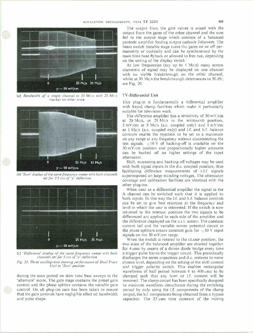
(a) Bandwidth
MIDDLETON: OSCILLOSCOPE, TYPE TF 2200 187
The output from the gate valves is mixed with the output from the gates of the other channel and the sum fed to the output stage which consists of a balanced pentode amplifier feeding output cathode followers. The beam switch bistable stage turns the gates on or off per- manently or cyclically and can be synchronized by the main time base flyback or allowed to free run, depending on the setting of the display switch.
At low frequencies (say up to 1 Mc/s) many screen diameters of signal may be displayed on one channel with no visible breakthrough on the other channel, whilst at 30 Mc/s the breakthrough deteriorates to 30 dB; see Fig. 20.
of a single channel to 35 Mcls with 25 Mc/s marker on other trace
(b) `Sum' display of the same frequency sweep with both channels set for 2.5 cm of 'y' deflection
(c) `Difference' display of the same frequency sweep with both channels set for 5 cm of 'y' deflection
Fig. 22. Three oscillograms showing performance of Dual Trace Unit in 'Sum' position
during the scan period on slow time base sweeps in the `alternate' mode. The gate stage contains the preset gain control and the phase splitter contains the variable gain control. On all plug -ins care has been taken to ensure that the gain controls have negligible effect on bandwidth and pulse shape.
TV-Differential Unit
This plug-in is fundamentally a differential amplifier with keyed clamp facilities which make it particularly suitable for television work.
The difference amplifier has a sensitivity of 50 mV/cm at 20 Mc/s, or 28 Mc/s in the WIDEBAND position, 5 mV/cm at 8 Mc/s (a.c. coupled only) and 1 mV/cm at 1 Mc/s (a.c. coupled only) and l.f. and h.f. balance controls enable the rejection to be set to a maximum on any range at any frequency without disconnecting the test signals. ± 10 V of backing -off is available on the 50 mV/cm position and proportionally higher amounts can be backed off on higher settings of the input attenuator.
Shift, measuring and backing -off voltages may be used with both signal inputs in the d.c. coupled position, thus facilitating difference measurements of v.l.f. signals superimposed on large standing voltages. The attenuator coverage and calibration facilities are identical with the other plug -ins.
When used as a differential amplifier the signal in the A channel can be switched such that it is applied to both inputs. In this way the 1.f. and h.f. balance controls can be set to give best rejection at the frequency and level in which the user is interested. If the switch is now returned to the NORMAL position the two signals to be differenced are applied to each side of the amplifier and the difference displayed on the c.r.t. screen. The constant current tail and the variable screen potential circuit in the phase splitters ensure constant gain for ±50 V input signals on the 50 mV/cm range.
When the switch is rotated to the CLAMP position, the two sides of the balanced amplifier are shorted together for 4 µsec by means of a driven diode bridge every time a trigger pulse leaves the trigger circuit. This periodically discharges the series capacitors and d.c. restores to some chosen level, depending on the setting of the shift control and trigger polarity switch. This enables rectangular waveforms of half period between 4 to 400 sec to be clamped such that any hum or l.f. content will be removed. The clamp circuit has been specifically designed to minimize waveform disturbance during the switching period by only using the l.f. components of the clamp output, the h.f. components being obtained from a bypass capacitor. The 33 sec time constant of the mixing

188 MARCONI INSTRUMENTATION VOL. 8 NO. 8
o. h;
o
\\
2.
f )f \}
17.
r-" \§ !
§
II
$}
--,
§
(
m I 11112
Æ

MIDDLETON: OSCILLOSCOPE, TYPE TF 2200
(a) Field display without clamp
x:- 50 µsec/cm y:- I V/cm
189
x:- 4 msec/cm y:- I V/cm
(b) Field display with clamp
I
"6"--. V
f !
S t1.1011110i.:a
x:- 50 µsec/cm y:- I V/cm
(c) Line display without clamp (d) Line display with clamp
Fig. 24. Television sync pulse train with four times its amplitude of added 50 c/s waveform
networks ensures that any fast switching transients are integrated and reduced to a very small amplitude whilst cathode followers stop the switching transients filtering into the h.f. bypass circuit.
Using this position a television signal can be clamped to sync bottom or blanking level regardless of d.c. variations or hum content and the use of this feature is more fully described in the next section. Of course, in this position, as with the a.c. coupled higher sensitivity positions, the measuring dial is inoperative and only graticule measurements can be made.
Television Uses
Although both the single trace unit and the dual trace unit have their uses for television work, only measure- ments using the TV-Differential Unit will be described as the operation of the former units is more self- evident.
If a composite video signal is applied to one input socket and the trigger mode switch set to TV INTERNAL a field locked display will result. On main time base normal setting both odd and even fields will be displayed alter- nately unless the time base is set slow enough to 'count- down', thus missing every other field. On all the delaying
sweep positions, however, a fixed waiting time of 30 msec (adjustable to 24 msec by customer control for 60 field/sec operation) is switched in on the TV position, thus display- ing only odd or even fields on sweep speeds faster than a field period. Depression of the beam locate button inter- rupts the sync and causes field change to occur on a random chance basis. This fixed waiting time enables the delayed display to be greatly enlarged when looking for test signals in the post field pulse region yet still maintaining odd or even field lock.
Individual portions of the waveform may now be examined either in the delayed or gated mode and if two lines on each field contain pulse and bar signals con- forming to certain timing requirements, these may be viewed in the superimposed sliding bar type display.
The Tv trigger position is a.c. coupled and d.c. restored so that d.c. shifts, hum, varying video content, will not affect synchronism.
For positive going video signals the trigger polarity switch must be in the positive going position to obtain field separation; this position of the switch will give line by line black level clamping. The choice of sync bottom or blanking level for clamping is available when triggering from line pulses; only blanking level clamping is possible in the field sync mode for video signals of either polarity.

190 MARCONI INSTRUMENTATION VOL. 8 NO. 8
Line by line pulse and bar measurements for equip- ment or line testing are particularly simple to make and a special `k' factor graticule to Post Office standards is available for quick assessment of the equipment rating. Pulse and bar generators can be set up absolutely with great confidence because of the wide bandwidth of the TF 2200. Changing the bandwidth from 20 Mc/s to 28 Mc/s by means of the TRANSIENT-WIDEBAND switch changes the height of a 625 line T pulse by about 1%; the WIDEBAND position being the one most nearly correct.
Because of the improved a.c./d.c. gain ratio, accurate black -to -white bounce measurements are possible. If the amplifier has been hard cut-off, say 10 V on the 50 mV/cm position, for 20 seconds and then instantly returned to zero voltage, the resulting trace drift over the next 20 seconds is typically less than 2 mm, i.e. 10 mV.
For differential measurements and for windowed signals in excess of two screen diameters, external sync must be used. All the internal features of TV field sync separator and line by line clamp operate; as the trigger circuit is fed via a d.c. restoration circuit, signals with up to 400% hum effect satisfactory synchronizing.
If the signal under test is (say) a 1 V p -p signal, at a 40 V d.c. potential, it can be displayed at one screen diameter by backing -off in the d.c. coupled position or by d.c. restoring with the clamp in the a.c. coupled position depending on the measurement requirements.
For differential measurements, the l.f. and h.f. balance adjustments enable the rejection to be set to about 40 dB even on complex waveforms and on any attenuator setting. This may be checked, if suspected, without disconnecting the signals under test.
All the above measurements can be made without any external links as the trigger circuit is arranged to feed the appropriate trigger pulses to both time bases. Should the user wish to operate the delaying time base completely separately from the main time base, a socket marked B EXT has been fitted so that if the trigger mode switch is set to B EXT a fast negative pulse fed into this socket will fire the delaying time base whilst the main time base operates from the trigger circuit as normal taking the feed either from internal or external sources.
Accessories
CATHODE FOLLOWER PROBE
This allows a.c. coupled measurements to be made on circuits remote from the oscilloscope with a loading of only 8 pF in parallel with 10 Mû. The connecting cable is matched at the far end with a 9152 resistor and at the near end by the 9052 output resistance of the valve. This method of connection causes a loss of half the signal but ensures good pulse response and a flat frequency response which is less than 0.5 dB in error at 30 Mc/s.
The output resistance of the valve will vary slightly from model to model, so that attenuation will not always be 2 : 1. To avoid the need for tedious arithmetic, a socket on the front panel provides a calibration signal of 0.5 V p -p which, when fed through the probe, allows the preset gain control on the plug-in in use to set the display to 5 cm. When this is done, all graticule voltage measurements must be multiplied by two to obtain the correct reading though, of course, the measuring dial will record the true cathode follower output which is not, in general, exactly half the signal.
The cathode follower circuit is essentially of the small signal, wideband type and the input signal should not exceed 3 V p -p for faithful reproduction, although up to 300 V can be applied without damage. The increase in distortion with signal amplitude is not very severe and some users might find it satisfactory up to 5 V p -p, although above the 3 V p -p level it is recommended that the passive 10 : 1 divider should be used as this has a very similar circuit loading and will give a screen diameter display at this level.
The probe is cylindrical in shape and measures approximately in. in diameter and 6 in. in length. It is d.c. heated to avoid open circuit hum pick-up.
10 : 1 DIVIDER PROBE
A passive 10 : 1 divider presenting a circuit loading of 8 pF in parallel with 10 Ma is also available. Resistance wire is used for the inner of the coaxial coupling cable to sufficiently attenuate reflections so that an acceptable frequency response is maintained up to 30 Mc/s.
ABRIDGED SPECIFICATION
Overall performance with: Sensitivity Ten ranges in 1-2-5 sequence from
SINGLE TRACE UNIT, TYPE TM 6455 50 mV/cm to 50 V/cm. Increased to 10 mV/cm up to 20 Mc/s.
Bandwidth Input Impedance TRANSIENT: (Overshoot less than 1 %: 1 Mn with 30 pF in shunt. d.c. to 30 Mc/s.
WIDEBAND: d.c. to 38 Mc/s.
Risetime
12 nsec for overshoot of less than 1%.
DUAL TRACE UNIT, TYPE TM 6456
Bandwidth TRANSIENT: (Overshoot less than 1 %): d.c. to 27 Mc/s. WIDEBAND: d.c. to 35 Mc/s.
Risetime 14 nsec for overshoot of less than 1%.
Sensitivity Ten ranges for each channel in 1-2-5 sequence from 50 mV/cm to 50 V/cm.
Input Impedance 1 MO with 27 pF in shunt.
Polarity Reversal To simplify comparison of signals 180` out of phase, the polarity of either channel can be inverted.

MIDDLETON: OSCILLOSCOPE, TYPE TF 2200 191
Display Selection Five position selection giving: ALT.
A
A+B
B
CHOP
Channels A and B displayed on alternate time base sweeps. Channel A only. Algebraic sum of both input chan- nels. Channel B only. Chopped display of both channels at 500 kc/s switching rate.
TV-DIFFERENTIAL UNIT, TYPE TM 6457
Bandwidth
TRANSIENT: (Overshoot less than 1 %): d.c. to 20 Mc/s. WIDEBAND: d.c. to 28 Mc1s.
Risetime 18 nsec for overshoot of less than 1 %.
Sensitivity Ten ranges for each channel in 1-2-5 sequence from 50 mV/cm to 50 V/cm. Increased to 5 mV/cm from 4 c/s to 8 Mc/s, and 1 mV/cm from 4 c/s to 1 Mc/s
Y AMPLIFLrR
Amplitude Measurement
By calibrated Y -shift potentiometer: Accuracy: ±2 % of full-scale dial reading at x 10. By calibrated graticule: Accuracy: ±3 %.
Signal delay
A signal delay of 0.18 psec is introduced by a balanced lumped -constant delay line. Permits observation of the leading edge of the waveform that triggers the sweep.
Hum level
Less than 0.5 mm width at 50 mV/cm sensitivity.
X AMPLIFIER
Bandwidth
2 c/s to 3 Mc/s.
Expansion x1 to x5.
Sensitivity 3.5 V/cm at x 1 expansion; 700 mV/cm at x 5.
External input
IMPEDANCE: 470 k(2, a.c. coupled with 025 µF capacitor.
Z MODULATION
INPUT REQUIREMENT: 1 to 3 V p-p depend- ing on frequency.
Function switch
A front -panel control selects any one of the following sweep conditions:
INPUT IMPEDANCE: 470 ko with 50 pF in NORMAL: Signal triggers Main Time Base shunt. which provides X -deflection.
SWEEP GENERATOR
Two time bases are available:
Main Time Base [A]
SWEEP VELOCITY: Twenty-four ranges in 1-2-5 sequence from 2 sec/cm to 50 nsec/ cm at minimum X expansion.
TIME MEASUREMENT: By calibrated X -shift potentiometer: Accuracy: ±2% of full-scale dial reading at x 10. By calibrated graticule: Accuracy: ±3%.
Delaying Time Base [B]
SWEEP vELocrrY: Six ranges in I-10-100 sequence from 100 cosec/cm to 1 .sec/cm at maximum velocity setting.
TIME MEASUREMENT: By calibrated 10 -turn helipot. Accuracy: ±2% of f.s.d. ±0.5
sec whichever is the greater.
Trigger facilities
INPUT MODES: EXT (B), TV, DC, AC, AUTO,
and HF; triggered from internal, external or supply -frequency sources, recurrent or single -shot. See table below.
TRIGGER LEVEL control windows two screen diameters on INTERNAL, and ± 10 V on EXTERNAL.
DELAY: Signal triggers Delay Time Base which, after adjustable delay, triggers Main Time Base. X -deflection provided either by Main Time Base, or by Delay Time Base with bright portion of trace showing duration of Main Time Base.
GATED: Signal triggers Main Time Base but the triggering action is delayed until gate is opened by Delay Time Base, and is closed after one sweep of the Main Time Base. X -deflection provided as under DELAY above.
MULTI TRIG: Signal triggers the Delay Time Base which opens gate and triggers the Main Time Base. Subsequent sweeps of Main Time Base are triggered by the signal until the Delay Time Base com- pletes its sweep and closes the gate. X -deflection provided as under DELAY
above.
EXT T/n: Horizontal deflection is provided by an external signal which is amplified by the X amplifier.
POWER SUPPLY
200 to 250 V or 100 to 130 V, 50 to 60 c;s; 600 W (with Dual -Trace Unit).
DIMENSIONS AND WEIGHT Height Width Depth Weight 17+ in 13 in 27$ in 73 lb
(44.5 cm) (33 cm) (70 cm) (33 kg)
Mode Internal Trigger Level
External Trigger Input Input Impedance
EXT (B) Main Time Base triggers as under A.C.
TV
D.C.
A.C.
AUTO
H.F.
Field lock on any TV waveform provided sync pulse amplitude on display exceeds 2 mm peak -to -peak deflection. Triggers from d.c. to 1 Mc/s for 2 mm, or to at least 5 Mc/s for 10 mm sinusoidal deflection. Triggers from 20 c/s to 1 Mc/s for 2 mm, or to at least 5 Mc/s for 10 mm sinusoidal deflec- tion. As A.C.
Used above 2 Mc/s for synchronizing time base. Synchronization obtained up to 25 Mc/s with 2 mm deflection, and up to 30 Mc/s with 10 mm deflection.
Several volts 10 kg) a.c. negative to coupled trigger D.T.B.
As `Internal' except read 0.5 V for 2 mm.
1 MO and 25 pF in shunt.
1 kO a.c. coupled.

192
MARCONI INSTRUMENTS
NEW
DESIGN
A 1% Sensitive Valve Voltmeter
by E. C. CRAWFORD, Graduate I.E.E.
621.317.72
This amplifier/rectifier voltmeter has a frequency range of 10 c/s to 5 Mc/s, with a measuring accuracy of ±1% of full-scale from 50 c/s to 500 kc/s. It has twelve voltage ranges with full-scale sensitivities from 1 mV to 300 V. The circuit is described in general terms and consideration given to design problems associated with voltmeters of this class.
TF 2600 is a new Sensitive Valve Voltmeter of the amplifier type with full-scale sensitivities ranging from 1 mV to 300 V, and a bandwidth of 10 c/s to 5 Mc/s. The design has placed emphasis on the highest accuracy in the most used part of its frequency spectrum, 50 c/s to 500 kc/s, while extending the frequency range, at reduced accuracy, to the useful limit achievable by the gain band- width product of the valves used.
Built into the instrument is an accurate attenuator which with the near -linear meter scale enables measure- ments of gain or attenuation to be made with precision.
Description of Circuit
The simplified circuit diagram shown in Fig. 1 outlines the general arrangement of the voltmeter. It can be seen that following the input attenuator there is a cathode follower stage which has a gain of approximately 0.95 and drives the medium impedance step attenuator. The amplifier following this attenuator always operates at constant gain, the input not exceeding 0.95 mV for full- scale deflection on the output meter. This amplifier has four valve stages with overall negative feedback from the fourth anode to the first cathode through the meter
O N
rectifier system, the negative feedback network containing elements which improve the response at the h.f. extreme of the pass band.
By arranging the feedback path through the meter rectifier, an enormous improvement in meter linearity is obtained compared with a straightforward detector which is subject to the non -linearity of the diodes. Since the pentode output stage has a relatively high anode load it tends to act as a constant current generator to feed the meter circuit in a linear manner even without the feed- back, but this system has its limitations in practice.
The amplifier valves are coupled by CR networks of carefully chosen time constants so that the rate of change of amplification and therefore the phase characteristic is under close control. No two time constants are the same, as if they were we should have a phase shift oscillator. These remarks about time constant apply equally to the low frequency couplings determined by the coupling capacitors and the grid leaks, and to the high frequency time constants determined by the anode load resistors and their shunt capacitance to earth. A typical phase and gain response for one particular stage is shown in Fig. 2.
With the overall frequency characteristic being mainly determined by the negative feedback it is not necessary or
030
0100
0300
-u
V2 V3 V4
+Vt BIAS
H.T.
VS
T
Fig. 1. Basic circuit diagram
N.F.B.
O AMP OUT
CRAWFORD: A I % SENSITIVE VALVE VOLTMETER
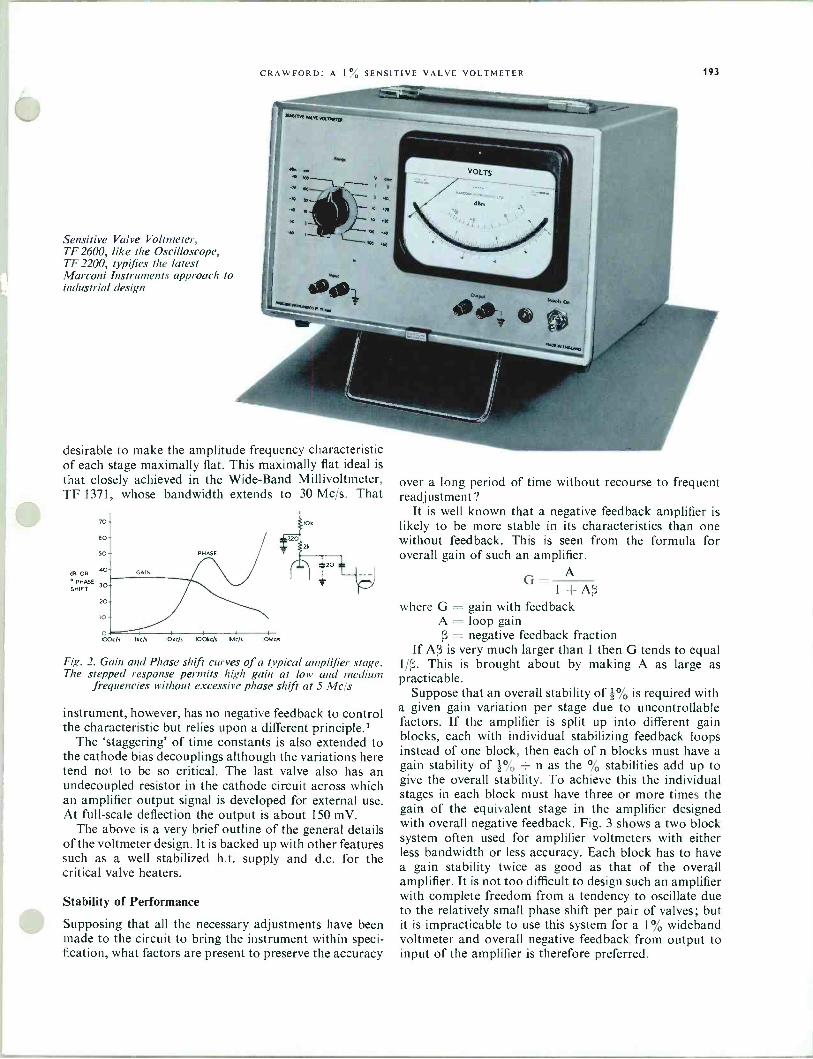
Sensitive Valve Voltmeter, TF 2600, like the Oscilloscope, TF 2200, typifies the latest Marconi Instruments approach to industrial design
desirable to make the amplitude frequency characteristic of each stage maximally flat. This maximally flat ideal is
that closely achieved in the Wide -Band Millivoltmeter, TF 1371, whose bandwidth extends to 30 Mc/s. That
70
60
SO
dB OR 40
PHASE 30
SHIFT
20
10
GAIN
PHASE
10Oc/s Ikc/s 10k ch IOOkc/s M1cJs 1
ION
22ò
T20
Fig. 2. Gain and Phase shift curves of a typical amplifier stage. The stepped response permits high gain at low and medium
frequencies without excessive phase shift at 5 Mc/s
instrument, however, has no negative feedback to control the characteristic but relies upon a different principle.'
The `staggering' of time constants is also extended to the cathode bias decouplings although the variations here tend not to be so critical. The last valve also has an undecoupled resistor in the cathode circuit across which an amplifier output signal is developed for external use. At full-scale deflection the output is about 150 mV.
The above is a very brief outline of the general details of the voltmeter design. It is backed up with other features such as a well stabilized h.t. supply and d.c. for the critical valve heaters.
Stability of Performance
Supposing that all the necessary adjustments have been made to the circuit to bring the instrument within speci- fication, what factors are present to preserve the accuracy
193
over a long period of time without recourse to frequent readjustment ?
It is well known that a negative feedback amplifier is likely to be more stable in its characteristics than one without feedback. This is seen from the formula for overall gain of such an amplifier.
A G 1+Aß
where G = gain with feedback A = loop gain ß = negative feedback fraction
If Aß is very much larger than 1 then G tends to equal 1/(3. This is brought about by making A as large as practicable.
Suppose that an overall stability of 4% is required with a given gain variation per stage due to uncontrollable factors. If the amplifier is split up into different gain blocks, each with individual stabilizing feedback loops instead of one block, then each of n blocks must have a gain stability of 4% _ n as the % stabilities add up to give the overall stability. To achieve this the individual stages in each block must have three or more times the gain of the equivalent stage in the amplifier designed with overall negative feedback. Fig. 3 shows a two block system often used for amplifier voltmeters with either less bandwidth or less accuracy. Each block has to have a gain stability twice as good as that of the overall amplifier. It is not too difficult to design such an amplifier with complete freedom from a tendency to oscillate due to the relatively small phase shift per pair of valves; but it is impracticable to use this system for a 1% wideband voltmeter and overall negative feedback from output to input of the amplifier is therefore preferred.

194
Fig. 3. A two block system with two feedback loops often used in volt- meters with a less exacting perform- ance specification
MARCONI INSTRUMENTATION VOL. 8 NO. 8
-IF
V2 V3
AM
In this voltmeter the value of Aß is about 56 dB or 600 times at mid -band. The overall accuracy is graded accord- ing to frequency and it is the mid -band region that most requires exceptional gain stability to maintain the 1% claim.
The feedback network itself comprises a rr network of stable metal film resistors with capacitive and inductive high frequency correction. The overall accuracy is of course proportional to variations of these resistors with time and temperature but the relatively low values that are used have very good stability comparable with wire wound types. Furthermore, in a low impedance network such as this, the inductance must be kept under very close control and must also be very low; conditions difficult to realize with wirewound resistors.
The cathode follower drives a medium resistance attenuator which provides 5 accurate 10 dB steps. This attenuator is made up from precision wire wound card type resistors with suitable capacitance compensation and with a carefully chosen balance between resistance and residual inductance. These resistors will therefore have the stability normally associated with careful manufac- ture, aging and adjusting techniques.
The input attenuator is made in a different way altogether. As the input resistance is 10 MSI, then a 10 MS2 resistor must figure in the attenuator. Attempts to simulate 10 M12 input resistance by application of negative feedback only leads to excessive noise. The only suitable component for this resistor, considering all aspects such as input capacitance and wide band response, is a cracked carbon film high -stability type. Metal film resistors of this value are not available as single units and a multiple element resistor leads to frequency response difficulties. The 10 MS2 resistor forms the first section of a 1000 : 1 divider and the second section comprises a fixed resistor, a temperature compensator and a small variable resistor; this section can be adjusted, by means of the variable resistor, to exactly 1/999 of the resistance of the particular 10 MS2 actually used.
This high resistance divider must be very stable as it sets the accuracy for half the available ranges of the volt- meter. The type of resistor actually specified in the design has been selected for its particularly good qualities, such as long term stability, low temperature coefficient, good frequency characteristic and rugged protection. The last
N.F.B.
FF
V4 V5
1 VA BIAS
H.T.
AMP
r-0 OUT
is vital, of course, as the actual carbon film on a small resistor of this value is very thin. Although the tempera- ture coefficient is low for its type, it still amounts to .05% per °C, which is quite a lot considering the possible operating environment and the initial warming up of the voltmeter from cold. The smaller resistor of the attenuator must inevitably have a different temperature coefficient as it depends upon the thickness of the carbon film used in the construction and this is greater for the lower values. In the present attenuator a thermistor and resistor com- bination is used so that the attenuation ratio remains as constant as possible with temperature changes. This is an unusual refinement in a voltmeter of this class.
While on the topic of temperature coefficient the detector diodes and the meter should not be overlooked. In some bridge rectifier circuits using resistors instead of capacitors for two arms of the bridge the normal meter coil, which has a large temperature coefficient, is shunted by the relatively stable resistors. In the TF 2600 circuit the capacitors effectively bypass the a.c. and it is easily demonstrated that a 100% change in meter resistance has no effect on the sensitivity. The diodes are too often a source of drift as the temperature varies and it is only in recent years that semiconductor development has pro- duced very high frequency silicon diodes with their virtually zero temperature sensitivity in a constant current circuit.
Of all the items in the instrument which are bound to change with time and use, the most obvious of all are the amplifier valves. This valve aging has very little effect upon the cathode follower, which has very high inherent d.c. and a.c. negative feedback so that it works at con- stant current despite aging and thereby produces almost drift free gain. There are two major stabilizing factors for the amplifier valves. The first is the very large overall negative feedback which has already been mentioned. This is most effective at mid -band where the loop gain of the amplifier is at its greatest value and where of course the basic accuracy of the voltmeter is highest. Towards the fringes of the passband the control of the feedback diminishes slightly and the effect of valve aging would be noticed but for the biasing arrangements used which tend to keep the valves working at constant current despite variations in cathode emission. A study of valve characteristics will show that the mutual conductance

CRAWFORD: A 1% SENSITIVE VALVE VOLTMETER
can remain almost constant provided that the proper relationship between grid bias and screen grid voltage is maintained at a constant cathode current. The mutual conductance of a valve may vary quite a lot from sample to sample of the same type, but once the valve is made and sealed it is rather rare for the physical relationship between the various electrodes to change and this mainly controls the working parameters.
Summation of Errors
In any voltmeter or other measuring instrument which has a quoted accuracy, or should we say quoted maxi- mum error, it is certain that this maximum error is the sum of a number of smaller errors. Considering any ordinary multi -range instrument, there are only two possible sources of error - the range resistors and the meter. The electronic multi -range voltmeter is in a different class and, owing to its more complex nature, is more prone to a multiplicity of errors than the simple electro -mechanical type.
First the meter: due to mechanical limitation and the inaccuracies of initial calibration, errors of up to 4 or 2% of full scale are to be expected. This can also include errors in the movement due to backlash or mechanical hysteresis, often the result of pivot roll or slight stickiness in the pivots. Basic non -linearity which can be caused by imperfect linearity of the magnetic field or mis -alignment of the moving coil is taken up by individual scale calibra- tion. Other errors of the scale law type are usually due to residual non -linearity of the diode rectifiers which increases at higher frequencies due to the shunting effect of stray capacitance.
The next group of errors which are nearly always linear (i.e. they do not vary with the amplitude of the signal) are due to the frequency response of the amplifier and various attenuators. Negative feedback improves the frequency response of an amplifier but its effectiveness falls off as the loop gain decreases, which means that the basic amplifier does not have a perfect frequency response. In this amplifier, the response is probably within % over the band 50 c/s to 500 kc/s, 1% up to 2 Mc/s, and 2% at 5 Mc/s; at the lower frequency end of the pass band the response is within 1% at 20 c/s and 2% at 10 c/s. This conservative basic amplifier response is therefore well within the overall specification and contains margins of
D.C. VOLTAGE
STANDARD
Fig. 4. The calibration system used. The reference voltmeter and r.f. attenuator are standard- ized at 400 c/s by comparison with the transformer system
195
safety for subsequent deterioration and other factors. These errors in the amplifier response are present, not only on the lowest range, but also on the higher ranges, which are derived by attenuating the signal prior to the amplifier.
Up to 300 mV there will be no difference in the response from the amplifier at frequencies up to 1 Mc/s because the attenuation is determined by the accurate 0.1% resistors. At the higher frequencies there is capacitance trimming which adjusts the response at each stage to be an optimum between 2 and 5 Mc/s; here again a conser- vative margin of safety of nearly 2 to 1 is obtained in the specification limits. Over 300 mV a 60 dB attenuator is introduced which is set to give the correct loss at all frequencies. The attention given to maintaining the temperature coefficient of this important attenuator has been described in the stability section.
So it can be seen that the instrument errors comprise two basic groups: the non-linear errors of the meter movement including the detector diodes, and the fre- quency response of the basic amplifier with or without the input attenuator sections. It has been described how the sum of these errors is less than the specification limits of the instrument.
Proving the Accuracy
A.C. voltmeters are more difficult to check than d.c. types because standard levels of a.c. voltage at various fre- quencies are not very common, and such as are available are often not convenient for one reason or another. D.C. voltages are established quite readily at medium and low levels by means of potentiometers which com- pare the voltage to be measured against a standard cell. The accuracy is limited by the standard cell, the resistance divider and, finally, any thermal e.m.f's or contact potentials present in the system. A final accuracy of .01% or thereabouts is now common.
An a.c. voltage is most accurately measured in terms of its r.m.s value by comparing it with d.c. in what is known as a thermal transfer standard. This may be a thermo- couple, thermistor bridge or lamp bridge. Provided that suitable precautions are taken accuracies approaching 02% may be realized although .05% is more common. Precautions that are necessary relate to the stability of the ambient temperature, avoidance of turnover effect
THERMAL
COMPARATOR
400 as SOURCE WITH
VERY PURE
WAVEFORM
TRANSFORMER DIVIDERS
Og\ a O ®6 o o -
O
--
3 00th
O 4 STANDARD
WIDEBAND
OSCILLATOR
J L
REFERENCE VOLTMETER
R.F.
ATTENUATOR
FULL SCALE o VOLTAGE
OUTPUTS
10c if TO 5Mch STANDARD OUTPUTS

196 MARCONI INSTRUMENTATION VOL. 8 NO. 8
due to thermal e.m.f's, and the use of suitable resistors which are virtually non -reactive at the frequency con- cerned. The method used is to measure the effect due to a known d.c. and then the a.c. is adjusted to have the same effect. It follows that the a.c. r.m.s. voltage is the same as the d.c. If the a.c. has a waveform free from har- monics it may be used to calibrate any voltmeter regardless of type; peak, mean level, or true r.m.s.
TF 2600 is calibrated in terms of r.m.s. voltage but its detector system is mean level. Using a generator with low harmonic content this gives almost exactly the same answer as the true r.m.s. voltmeter if the waveform has mostly second harmonic, but is susceptible to third harmonic error to a degree dependent upon the phase relationship. The worst error is about one third the per- centage third harmonic content; i.e. 3% third harmonic gives a reading error of 1% compared with true r.m.s.
The system adopted for calibration purposes, illustrated in Fig. 4, is to establish with an accuracy of 0.1% the absolute level of a 400 c/s oscillator of very pure wave- form by means of an a.c./d.c. thermal comparator. As it was found impracticable to use the same thermal system for all the frequencies 10 c/s to 5 Mc/s for a number of reasons, a further voltmeter called the reference voltmeter is standardized using the known 400 c/s source.
This reference voltmeter is a mean level type using two u.h.f. crystal diodes and operates only at the fixed level of
Voltage range 0 to 300 V in 12 ranges, with full-scale deflections of 1, 3, 10, 30, 100, and 300 mV, and 1, 3, 10, 30, 100, and 300 V.
Frequency range 10 c/s to 5 Mc/s, with a useful response to 10 Mc/s.
Measurement accuracy +1% of full scale, 50 c/s to 500 kc/s,
1 V. It lends itself to a system of scale expansion which gives almost 10 times the discrimination of the TF 2600. There is therefore no practical further loss of accuracy in this second transfer. Again, by having a mean level voltmeter as the wide band reference, there is the same susceptibility to any waveform errors from the wide band oscillator as the instrument under test.
To esta blish the accuracy of the TF 2600 on all its ranges there is a system of transformer dividers operating only at 400 c/s which ensure that the basic 400 c/s accuracy is not lost. This transformer system produces full-scale voltages from 1 mV to 300 V and also voltages in a 0, 1, 2, 3, 4-10 sequence for scale linearity checks.
With the 400 c/s absolute level as a reference on any range, the deviations of the TF 2600 readings from this reference may now be measured at other frequencies using the reference voltmeter as a monitor followed by an r.f. 75 f1 attenuator. In this application, the absolute accuracy of the attenuator is not of primary importance -only its frequency characteristic. This attention to the details of calibration has been found necessary for this particular instrument in order to prove that the close accuracy obtained by careful design is achieved and maintained in practice.
REFERENCE 1. White. L. G.: ' Wide -Band M illivoltmeler, TF 1371', Marconi Instrumentation
1960, 7, p. 208.
ABRIDGED SPECIFICATION
+2% of full scale, 20 c/s to 1 Mc/s, ±3 % of full scale, 20 c/s to 2 Mc/s, +5% of full scale, 10 c/s to 5 Mc/s.
Calibration The meter is calibrated in terms of r.m.s. value of a sinewave, but responds to average value. Also calibrated in decibels relative to 1 mW in 600 0, over the range -72 to +52 dBm.
Input impedance
10 Mn, shunted by about 16 pF on 1 to 300 V ranges, and by about 30 pF on 1
to 300 mV ranges.
Amplifier output
Output on any range for full-scale deflec- tion on meter, approx. 150 mV; maxi- mum output 300 mV. Output impedance 51 0.
A NEAT BINDER to contain copies of Volumes 8 and 9 of Marconi Instrumentation has now been made available so that readers and librarians may keep copies of the bulletin in a convenient form for reference. It is bound in red rexine and copies can be inserted without punching and opened flat. These binders are available at a cost of 12s. each, post free. To simplify the transaction please send remittances when ordering.

Summaries of Articles appearing in this issue RESUME D'ARTICLES PUBLIES DANS LE PRESENT NUMERO
OSCILLOSCOPE TF 2200 L'oscilloscope TF 2200 est un appareil, de 35 MHz d'usage
courant, conçu spécialement pour mesurer les formes variées d'ondes de télévision.
L'adaptabilité de l'appareil est étendue, d'une part, par l'apport d'un nombre de tiroirs pré -amplificateurs sur le circuit de l'axe des temps `Y'; d'autre part, l'existence d'un système de retard de la base des temps, muni d'un choix judicieux de déclenchement permet de faire des mesures précises, même sur les formes d'ondes les plus compliquées.
On a cherché sérieusement à réduire le nombre de boutons de contrôle, de façon à simplifier le réglage de l'oscilloscope sans en réduire d'aucune façon le champ d'application.
L'élimination des boutons de contrôle pour la stabilité de l'image ainsi que celle des cordons à fiches de prise de courant s'emboîtant dans le devant de l'oscilloscope sont deux exemples de l'effort fait pour simplifier l'appareil.
197
Enfin, on peut se servir soit de l'écran gradué en cm., ou employer le retard des temps, pour effectuer des mesures sur la tension et le temps, dependant de l'exactitude demandée. La calibration de l'écran peut aussi être vérifiée sans coupler la prise de signal.
Page 171
VOLTMÈTRE A LAMPE SENSIBLE TF 2600 Ce voltmètre du type amplificateur -redresseur possède une
gamme de fréquence de 10 Hz à 5 MHz, avec une précision de mesure de +1 % à pleine échelle de 50 Hz à 500 KHz. Il possède douze échelles de tension indiquant des sensibilités de déflection totale de 1 mV à 300 V. Le circuit y est décrit en termes généraux et on y examine aussi les problèmes de construction relatifs aux volt- mètres de cette classe.
ZUSAMMENFASSUNG DER IN DIESER NUMMER ERSCHEINENDEN BEITRÄGE
OSZILLOGRAPH TF 2200 Dies ist ein Vielzwecke -Messoszillograph mit 35 MHz Band-
breite. Er wurde zur Durchführung von Fernsehmessungen mit besonderen Einrichtungen versehen. Eine Reihe von einsteckbaren Y -Vorverstärkern ergibt eine grössere Vielseitigkeit. Eine ver- zögernde Ablenkschaltung mit einer Vielzahl von Auslösemöglich- keiten gestattet die Durchführung genauer Messungen selbst bei den kompliziertesten Schwingungsformen.
Es wurde nichts unversucht gelassen, um die Zahl der vorein- gestellten Bedienungsmittel zu verringern und die Handhabung des Oszillographen einfach zu gestalten, ohne dabei irgendwelche Einrichtungen fortzulassen, die man bei einem solchen Gerät erwartet. Zwei Beispiele dafür sind der Fortfall der Stabilitäts'- Einstellung und die Abschaffung von sonst notwendigen Verbin- dungsbrücken an der Vorderseite des Gerätes.
Page 192
Je nach der verlangten Genauigkeit können Spannungs- und Zeitmessungen mit der Zentimeterskala auf der Schirmmaske oder mit Hilfe der Verschiebungsmethode durchgeführt werden. Die Eichung der Skala auf der Schirmmaske kann ohne Abschaltung des Eingangssignals durchgeführt werden. Seite 171
EMPFINDLICHES RÖHRENVOLTMETER TF 2600 Dieses verstärkende und gleichrichtende Röhrenvoltmeter hat
einen Frequenzbereich von 10 Hz bis 5 MHz. Die Genauigkeit beträgt ± 1 % des Skalenendwertes im Bereich von 50 Hz bis 500 kHz. Zwölf Spannungsmessbereiche mit Vollausschlägen von 1 mV bis 300 V sind eingebaut. Die Schaltung wird in allgemeiner Form beschrieben und die bei Spannungsmessern dieser Güteklasse auftretenden Fragen der Konstruktion werden behandelt.
Seite 192
SOMMARIO DEGLI ARTICOLI PUBBLICATI IN QUESTO NUMERO
OSCILLOSCOPIO TF 2200 E' un oscilloscopio di misura di uso generale, particolarmente
adatto per misure di forme d'onda televisive su 35 MHz. Una serie di preamplificatori per l'asse Y del tipo a innesto ne estende la versatilità, mentre una base dei tempi con ritardo, provvista di una serie completa di dispositivi di sgancio, permette l'esecuzione di misure precise anche su forme d'onda le più complesse.
Il numero delle regolazioni semifisse è stato ridotto al minimo e l'uso dello strumento è stato reso il più semplice possibile, senza rinunziare ad alcuna delle prestazioni proprie di strumenti di questa classe. Ad esempio, la `regolazione di stabilità' è stata eliminata, mentre non si richiedono connessioni sul pannello frontale.
Le misure, di tensione e di tempi, possono effettuarsi sia con riferimento ad un reticolo calibrato in centimetri sia per compen-
sazione, a seconda della precisione richiesta. La calibrazione del reticolo pub essere verificata senza disconnettere il segnale di ingresso. Pagina 171
VOLTMETRO A VALVOLA AD ALTA SENSIBILITA, TF 2600
Questo voltmetro amplificatore e reddrizzatore copre l'intervallo di frequenze da 10 Hz a 5 MHz, con una precisione di misura del +1 % del valore di fondo scala per frequenze da 50 Hz a 500 kHz. Ha dodici intervalli di tensione con una sensibilità in fondo scala da 1 mV a 300 V. Il circuito viene descritto in termini generali, ed i problemi di progettazione connessi con voltmetri di questa classe vengono considerati. Pagina 192
RESUMENES DE ARTICULOS QUE APARECEN EN ESTE NUMERO
OSCILOSCOPIO TF 2200 Un osciloscopio para mediciones generales en 35 MHz diseñado
con caracteres precisos para el uso de mediciones de la forma de onda en televisión.
Una cantidad de pre -amplificadores `Y' intercambiables extienden su versatilidad mientras un circuito de tiempo demorado con facili- dades comprensivas de disparo hace que se puedan obtener medi- ciones de las más complejas formas de onda.
Se ha hecho todo lo posible para disminuir el número de controles pre -ajustados y hacer sencillo el uso del osciloscopio sin sacrificio ninguno de las facilidades que se puedan esperar de obetener con tal instrumento.
La eliminación del control de `stabilidad' y la necesidad de eslabones de panel son dos ejemplos de esto.
Retículo de centímetro y medidas de `slide -back' se pueden obtener tanto de voltaje como de tiempo, dependiendo en la exactitud requerida y calibración de retículo pueden ser compro- badas sin desconexión de la señal de entrada. Página 171
VOLTÍMETRO SENSITIVO A VALVULA TF 2600 Este voltímetro del tipo amplificador -rectificador posee una gama
de frecuencia de 10 Hz a 5 M Hz, con una exactitud de medida de +1 % a plena escala. Tiene doce márgenes de tensión con sensibili- dades de 1 mV a 300 V a plena escala. El circuito se describe en términos generales, examinando especialmente los problemas de construcción que presentan los voltímetros de esta clase.
Página 192

198
Index to Volume Eight
GUIDE TO PAGE NUMBERS
MARCH 1961 .. 1-24 MARCH 1962 .. 97-120
JUNE 1961 25-48 JUNE 1962 .. 121-144
SEPTEMBER 1961.. 49-72 SEPTEMBER 1962 145-168
DECEMBER 1961 .. 73-96 DECEMBER 1962 169-199
A
Page
L
Page
A.C. Power Measurement Using an Oscilloscope 157 Limited by Noise . 46 Aerial Design for Power Measurement 150 Low Frequency Generator, TF 1382 .. . 64 Alignment of Modern Communication Receivers using
TF 144H and TF 1104 40 M Analogues and Digits .. 73 Measurement of Fast Pulse Rise Times 45 Applications 121 High -Value Electrolytic Capacitors 163 Attenuator, TF 1073A Series 130 Modification to Improve A.C. Zero Setting of TF 1300 17
B N
Bridges, Special .. 11 Nanosecond Pulse Generator, TF 1389 105 New 600 -Ohm Attenuator for the TF 1073A Series, A 130
Helical Coupled Noise Source, A 67 C Counter/Frequency Meter, TF 1417 ..
Range Extension Unit, TF 1434 Crystal Calibrator, TF 1374 & /1 ..
80 86 56
Look, The .. Noise Generator, TF 1301 ..
Measuring Set, OA 1249B
1
67 14
Standardization .. 44 O Oscillator, l.f., TF 1370 .. 3
D v.l.f., TF 1382 .. 64 Delay Generator, TF 1415 .. 115 Oscilloscope, TF 2200 . .. 171 Deviation Meter Standardization 16 for A.C. Power Measurement .. 157 Dielectric Test Set, TF 704C .. 138 Pre -Amplifier TM 6591 .. .. 42 Double Pulse Generator, TF 1400 . 99
Use of Oscilloscope as 113 P pH Meter as a Bridge Detector, A .. 128
E Power Measurement, A.C., using an Oscilloscope 157
Electrolytic Capacitor Measurement .. 163 Aerial Design for 150
Extended Q -Meter Measurement and Measurement Accuracy 61 Pre -amplifier for Oscilloscope, TM 6591 42 Pulse Generator, TF 1389 105
F Finger on the Pulse .. 97
TF 1400 Rise Time Measurement ..
99 45
F.M. Signal Generator, TF 1066B/2 .. 18
Frequency Meter, Digital, TF 1417 .. 80 Q Q -Meter, Extended Measurement and Accuracy .. 61
G Gamma Radiation Monitor, TF 1299.. 39
R Radar .. 25 R -C Oscillator, TF 1370 3
H Radiation Monitor for Gamma Rays, TF 1299 36 H.F. Spectrum Analyser, OA 1094A .. 88 Microwaves, TF 1396A 147
Receiver Alignment using TF 144H and TF 1104 40 I R.F. Radiation Power Meter, TF 1396A .. 147
Is a High Output Signal Generator Always Necessary? 156 Aerials .. 150

INDEX TO VOLUME EIGHT
Page
S U
199
Page
S -Band Spectrum Analyser TF 1387 27 U.H.F. Signal Generator, TF 1060/2 .. 123
Seeing is Believing . . 169 Signal Generator h.f., TF 144H 51
TF 867A 127 V high output considerations 156 Vacuum Tube Voltmeter, TF 1041C 75
ef u.h.f., TF 1060/2 .. TF 1066B/2 . .
123 18
TF 1300 .. TF 2600 ..
35 192
,
31 v.h.f., TF 1064 Series TF 1064B/5, /6, /7 and /8
57 132
V.H.F. Signal Generator, TF 1064 Series .. TF 1064B/5, /6, /7 and /8
57 132
,
X -band, TF 1343A Series .. 31 Voltmeter, Suppressed Zero, TF 1377 . . 159
Specialization . 145 Spectrum Analyser, h.f., OA 1094A .. 88
ef S -band, TF 1387 .. Standard Signal Generator TF 144H ..
TF 867A . .
Standardization of Crystal Calibrators,TF 1374 and TF 1374/1
27 51
127 44
W White Noise Test Set, OA 1249B Wide Range Double -Pulse Generator, A
R -C Oscillator, TF 1370 . .
.. 14 .. 113 .. 3
F.M. Deviation Meters 16
Suppressed Zero Voltmeter, TF 1377 .. Sweep Generator, TF 1099
159 30
X X -Band Signal Generator, TF 1343A Series . 31
T Test Set, Dielectric, TF 704C .. . .. 138 1
Transmitter and Receiver Output, TF 1065A .. 135 1% Sensitive Valve Voltmeter, TF 2600 .. 192 White Noise, OA 1249B .. 14
Transformer Testing for Instrument Reliability .. .. Ill Transmitter and Receiver Output Test Set, TF 1065A .. 135 2 Two Special Bridges .. . .. 11 20 Mc/s Sweep Generator, TF 1099 .. .. 30
INDEX BY TYPE NUMBERS
Page Page
TF 144H Standard Signal Generator, for Receiver Align- TF 1300 Vacuum Tube Voltmeter, Modification to ment 40 Improve A.C. Zero Setting .. 17
TF 144H Standard Signal Generator 51 TF 1300 Vacuum Tube Voltmeter, A.C. Multiplier and TF 704C Dielectric Test Set 138 Balanced Probe 35
TF 867A Standard Signal Generator 127 TF 1301 Noise Generator .. 67
TF 1041C Vacuum Tube Voltmeter TF 1060/2 U.H.F. Signal Generator
75 123
TF 1343A (series) X -Band Signal Generator
TF 1370 Wide Range R -C Oscillator 31
3 TF 1064 (series) 1374
V.H.F. Signal Generator 57 TF and /1
Crystal Calibrator 44 TF 1064B/5, /6, /7 and /8 TF 1374 and /1
V.H.F. Signal Generator 132 Crystal Calibrator, Standardization of .. 56 TF 1065A Transmitter and Receiver Output Test Set 135 TF 1377 Suppressed Zero Voltmeter .. 159
TF 1066B/2 F.M. Signal Generator 18 TF 1382 Low Frequency Generator .. 64 TF 1073A (series) TF 1387 S -Band Spectrum Analyser .. 27
Attenuator . 130 TF 1389 Nanosecond Pulse Generator .. 105
TF 1093 pH Meter as a Bridge Detector .. 128 TF 1396A R.F. Radiation Power Meter .. 147
OA 1094A H.F. Spectrum Analyser . . 88 TF 1400 Double Pulse Generator .. .. 99 TF 1099 20 Mc/s Sweep Generator, Extending Upper TF 1415 Delay Generator .. .. .. 115
Limit to 24 Mc/s 30 TF 1417 Counter/Frequency Meter .. .. 80 TF 1104 Television Sweep Generator, for Receiver TF 1434 Counter Range Extension Unit .. .. 86
Alignment 40 TF 2200 Oscilloscope .. .. .. .. 171
OA 1249B White Noise Test Set . 14 TF 2600 1 % Sensitive Valve Voltmeter .. .. 192
TF 1299 Gamma Radiation Monitor 36 TM 6591 Oscilloscope Pre -Amplifier .. .. 42

MARCONI INSTRUMENTATION
is published as a service to engineers who are interested in instrument technology and is sent to readers throughout the world.
If you have a colleague who might like to receive a regular copy of our bulletin
ask him to write to us.
MARCONI INSTRUMENTATION
is written by engineers for engineers and is issued quarterly
without charge.
D

A1
ut{{ iFi 1 frell
I
4+ I ; , , Iv = ; ' 'r *.
. "'rym 'S 1`-i76F cc_iR `mi - rap, ., ' I. ,
i:7 c' .. aL 5. r

SIGNAL GENERATORS
NOISE GENERATORS
OSCILLATORS
OSCILLOSCOPES
PULSE GENERATORS
MODULATION METERS
DISTORTION ANALYSERS
SPECTRUM ANALYSERS
FREQUENCY COUNTERS AND METERS
POWER METERS
VOLTMETERS
IMPEDANCE BRIDGES, DIELECTRIC AND Q METERS
MOISTURE METERS
pH METERS
IMAGE AMPLIFIERS FOR INDUSTRIAL AND MEDICAL X-RAY EQUIPMENT
ATOMIC POWER INSTRUMENTATION
MARCONI INSTRUMENTS 111 Cedar Lane Englewood, N.J.
Mr. A. Browdy, C. E. KCOP-TV
1962 So. Stearns Dr. Los Angeles 34+, Calif.
Return Requested
BULK RATE U.S. POSTAGE
PAID Englewood, N.J. Permit No. 313
MARCONI INSTRUMENTS LIMITED
SALES AND SERVICE OFFICES
London and the South ENGLISH ELECTRIC HOUSE, STRAND, LONDON, W.C.2 Telephone: Covent Garden 1234 Telex: 22572
Midland MARCONI HOUSE, 24 THE PARADE, LEAMINGTON SPA Telephone: Leamington Spa 25212 Telex: 31583
Northern 23/25 STATION SQUARE, HARROGATE Telephone: Harrogate 67454 (2 lines) Telex: 5723
Service Division HEDLEA WORKS, HEDLEY ROAD, ST. ALBANS
Telephone: St. Albans 50731 (4 lines) Ansafonc
U.S.A.
111 CEDAR LANE, ENGLEWOOD, NEW JERSEY Telephone : LOwell 7-0607
Head Office and Works
ST. ALBANS HERTFORDSHIRE ENGLAND Telephone: St. Albans 59292 Telex: 23350 Telegrams: Measurtest, St. Albans, Tele
ASSOCIATED COMPANIES AND DISTRIBUTORS THROUGHOUT THE WORLD
Printed in England by The CampJield Press
St. Albans