manufacturing an environmentally friendly pcb using ... · pdf filerobotics and...
TRANSCRIPT
ARTICLE IN PRESS
0736-5845/$ - se
doi:10.1016/j.rc
�CorrespondE-mail addr
Robotics and Computer-Integrated Manufacturing 23 (2007) 720–726
www.elsevier.com/locate/rcim
Manufacturing an environmentally friendly PCB using existingindustrial processes and equipment
A. Ryan�, H. Lewis
Manufacturing and Operations Engineering Department, University of Limerick, Castletroy, Limerick, Ireland
Abstract
This paper investigates the possibility of utilising an additive screen printing process with conductive ink and adhesive together with a
degradable substrate to identify whether this process offers a viable alternative to current subtractive methods of PCB manufacture.
Existing manufacturing equipment and production process were adopted in order to establish the compatibility of a sustainable and
environmental friendly PCB with these processes. Experimental trials have shown that by using a stainless steel stencil 150mm thick in
conjunction with an MPM Ultraprint machine with a printing speed of 89mm/s, a squeegee pressure of 0.97 bar and a downstop of
1.9mm successful printing of the electrically conductive adhesive was achieved. It was also shown that the substrate was compatible with
electronic placement technology and convection oven. Comparisons of the electronic assemblies to an industrial IPC standard illustrated
that it is possible to develop a circuit, which is deemed acceptable under this standard. It can be concluded therefore that a screen printed
conductive ink pattern, when printed on a degradable substrate can offer a viable alternative to current printed circuit boards and can be
manufactured using existing technology and manufacturing processes.
r 2007 Published by Elsevier Ltd.
Keywords: PCBs; Screen printing; Conductive inks
1. Introduction
This paper is concerned solely with examining thecompatibility of a silver conductive ink tracks and adegradable paperboard substrate with the PCB manufac-turing process, the robustness of the substrate itself will beanalysed in future work. The initial section of this paperillustrates the extent of the environmental problemassociated with the electronics industry and identifies theneed to change the status quo.
Due to advances and progress in technology, electricaland electronic equipment rapidly becomes dated andobsolete this is reflected in the volume of waste electricaland electronic equipment (WEEE) being deposited inlandfills sites across the European Union (EU). It hasbeen estimated that, prior to EU enlargement, each citizenof the 15 member states generated 23 kg of electrical/
e front matter r 2007 Published by Elsevier Ltd.
im.2007.02.009
ing author.
ess: [email protected] (A. Ryan).
electronic waste per annum [1]. While Hansen andLeipprand identified that the quantity of WEEE generatedannually increases by a rate of 16%–28% per annum [2].As printed circuit boards are constituents of most electricalequipment it is natural to assume that large volumes ofboards are being disposed of in landfill sites. Indeed a UKgovernment body, envirowise, found that during 2002 over6500 tonnes of manufactured PCBs from products such astelecoms and computers are discarded each year [3]. This isa substantial quantity of waste entering landfills and theEuropean Commission intends to address this mountingproblem through the introduction of the WEEE [4] andrestriction on hazardous substances (RoHS) [5] directives.These directives have forced manufacture’s to focus on theenvironmental impacts of their products and throughimposing penalties and by making the use of certainmaterials, such as lead, illegal the EC hopes to ultimatelypreserve the environment. The WEEE directive (2002/96/EC), hopes to limit the quantity of electrical and electronicwaste entering landfill through the promotion of the threeR’s of waste minimisation: reduce, reuse and recycle.

ARTICLE IN PRESSA. Ryan, H. Lewis / Robotics and Computer-Integrated Manufacturing 23 (2007) 720–726 721
The aim of this research is to use these three R’s todevelop a sustainable and environmentally acceptableprinted circuit board by screen printing a silver conductiveink onto a degradable substrate. Earlier work, by theauthors [6], has shown that it is possible to reproduce PCBtracks of known length and width accurately andinterruption free. It has also been established that whencertain printing and post-printing techniques are adoptedthat it is possible to achieve a conductive performancecomparable to that of existing copper boards.
However in order to ensure that the developed novelboard has actual industry merit it was necessary to ensurethat it was compatible with existing manufacturingequipment and processes. To this end and in conjunctionwith Kostal Ireland it was decided to reproduce an existingcopper board using the new technique, to screen print anelectrically conductive adhesive to facilitate the surfacemounting of components, to use an automatic pick andplace machine to mount the components and to curethe board through a reflow oven. The manufacturedboards were then analysed under Section 12.2.2 of IPC-A-610 C, acceptability of electronic assemblies [7]. Thiswould establish if the process was practical and indeedviable, the results of this investigation are detailed in thispaper.
2. Manufacturing process and equipment
2.1. Manufacturing process overview
The manufacturing process for the development of anenvironmental printed circuit board is designed as a ‘‘dropin’’ replacement for existing PCB manufacturing methods,and is detailed in Fig. 1.
Cure the adhesive throughConvection oven
Automatically place surfacemount components
Screen PrintElectrically Conductive
Adhesiveon interconnecting pattern
Screen Printinterconnecting pattern withelectrically conductive ink
Fig. 1. The manufacturing process overview.
From this figure it is apparent that the initial step is toreproduce the desired interconnecting pattern by screenprinting the pattern onto the specified substrate.Once the pattern has been created it is then possible to
print the electrically conductive adhesive (ECA) withprovides both an electrical connection and an adhesivebond between the surface mount component and theinterconnecting pattern.Having printed the ECA the next step is to automatically
place the surface mount components; in this case acomponent placement machine was employed.The final step of the process is to cure the electrically
conductive adhesive, this is achieved by running the printedboard through the solder reflow oven at a specifictemperature for a designated period of time.With a brief description of the overall manufacturing
process provided, the next section will detail the manu-facturing settings necessary to achieve accurate printingand placement both of the conductive ink and surfacemount components. It will also outline the physicalcharacteristics of the electrically conductive adhesiveand ink.
2.2. Interconnecting pattern
In order to establish if the technique outlined in Section2.1 offers a real and viable alternative to the subtractivemethod of PCB manufacture a datum board, consistingof typical track widths and lengths, was used in theseexperiments, the interconnecting pattern is shown inFig. 2. This is a standard printed circuit board which iscurrently in production, by using such a board it will bepossible to determine both the performance of theenvironmentally friendly boards (Fig. 3) but more im-portantly if the new production technique is compatiblewith existing equipment and manufacturing methods.
2.3. Screen printing
Screen printing uses a printing screen or stencil whichconsists of a frame onto which is stretched a fabric meshwith open apertures in the screen forming the design orcircuit to be printed. As the ink or coating is forcedthrough the open design (by a squeegee), the interconnect-ing pattern of the screen is replicated on the substrate [8].This printing process is illustrated in Fig. 4.
Fig. 2. Interconnecting pattern of existing PCB.

ARTICLE IN PRESS
Fig. 3. Interconnecting pattern of PCB printed on paperboard.
Screen Printing Machine
Substrate
Squeegee
Original ScreenPosition
Screen Printing Diagram
Screen Frame
Snap Off
Direction of Squeegeetravel
Fig. 4. Schematic of the screen printing process.
Fig. 5. MPM ultraprint.
A. Ryan, H. Lewis / Robotics and Computer-Integrated Manufacturing 23 (2007) 720–726722
The screen printing process is essentially a simpleefficient method of reproducing patterns on a variety ofsubstrates, which include plastics, fabrics, metals andpapers. However the key to screen printing reliableelectronic circuits depends on monitoring the printingparameters and maintaining specified limits. These limitsdetermine if the print will be successful and indeed whichprocess parameter settings offer the best opportunity toprint error free. When screen printing, there are a numberof key operating parameters of which screen type (meshand emulsion thickness) conductive ink properties (viscos-ity, particle size and solids content) are among the mostimportant.
For screen printing the interconnecting pattern detailedin this paper a conductive ink of 1.62 Pa s viscosity and asolids content of 6872% was employed together with asteel screen of mesh thickness 200 mm and an emulsionthickness of 18mm. Previous work by the authors [9] hasshown that a snap-off of 1mm, a squeegee hardness of 70shore, a pressure 0.41 bar and 0 s standing time results inthe best alternative when printing onto the degradablesubstrate. These operating settings were adopted whenreproducing the interconnecting pattern detailed in Fig. 3.
As has been detailed previously in order to bond thecomponents to the interconnecting pattern it is necessary touse an electrically conductive adhesive. This adhesive isalso screen printed into position, a stainless steel stencil150-mm thick with desired laser cut apertures was used inconjunction with an MPM Ultraprint machine (Fig. 5). Itwas found that a printing speed of 89mm/s, a squeegeepressure of 0.97 bar and a downstop of 1.9mm allowed forsuccessful printing of the adhesive. As is typical with the
printing of adhesives and solder paste contact printing wasused, by this it is meant that the stencil is in direct contactwith the substrate during printing and that the snap offheight is therefore zero.With the method of ink and adhesive deposition outlined
and explained the following section details the method ofautomatic component placement.
2.4. Automated placement of surface mount components
Manual placement of surface mount components isoperator dependant and as a result is unreliable, inaccurateand uneconomical. For prototyping purposes it is possibleto manually mount components however for large-scaleproduction of even the simplest circuits it is impractical, tothis end it was necessary to ensure that the environmentallyfriendly PCB was compatible with automated placementmachines. Concerns regarding the flexibility and rigidity ofthe substrate arose prior to experimentation and as such anumber of initial investigations were performed to providethe operating settings, which provided a successfulrelationship between accuracy of placement and speed ofplacement.To ensure maximum accuracy in the placement of
components a vision system is used to tell how far acomponent lead is from the corresponding land and to
ARTICLE IN PRESS
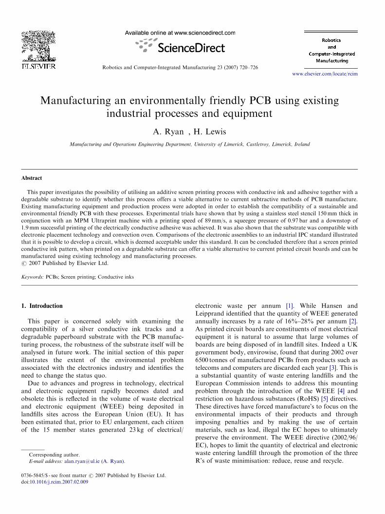
Fig. 6. The feducial used to teach the automated placer.
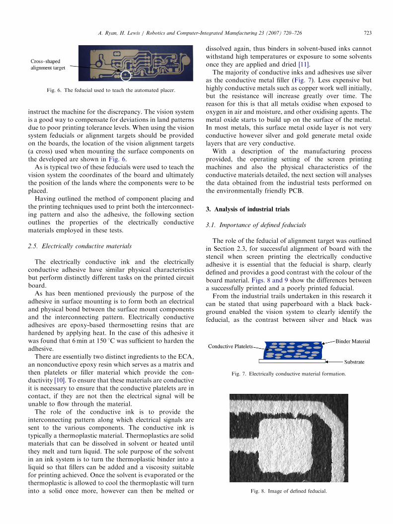
Fig. 7. Electrically conductive material formation.
Fig. 8. Image of defined feducial.
A. Ryan, H. Lewis / Robotics and Computer-Integrated Manufacturing 23 (2007) 720–726 723
instruct the machine for the discrepancy. The vision systemis a good way to compensate for deviations in land patternsdue to poor printing tolerance levels. When using the visionsystem feducials or alignment targets should be providedon the boards, the location of the vision alignment targets(a cross) used when mounting the surface components onthe developed are shown in Fig. 6.
As is typical two of these feducials were used to teach thevision system the coordinates of the board and ultimatelythe position of the lands where the components were to beplaced.
Having outlined the method of component placing andthe printing techniques used to print both the interconnect-ing pattern and also the adhesive, the following sectionoutlines the properties of the electrically conductivematerials employed in these tests.
2.5. Electrically conductive materials
The electrically conductive ink and the electricallyconductive adhesive have similar physical characteristicsbut perform distinctly different tasks on the printed circuitboard.
As has been mentioned previously the purpose of theadhesive in surface mounting is to form both an electricaland physical bond between the surface mount componentsand the interconnecting pattern. Electrically conductiveadhesives are epoxy-based thermosetting resins that arehardened by applying heat. In the case of this adhesive itwas found that 6min at 150 1C was sufficient to harden theadhesive.
There are essentially two distinct ingredients to the ECA,an nonconductive epoxy resin which serves as a matrix andthen platelets or filler material which provide the con-ductivity [10]. To ensure that these materials are conductiveit is necessary to ensure that the conductive platelets are incontact, if they are not then the electrical signal will beunable to flow through the material.
The role of the conductive ink is to provide theinterconnecting pattern along which electrical signals aresent to the various components. The conductive ink istypically a thermoplastic material. Thermoplastics are solidmaterials that can be dissolved in solvent or heated untilthey melt and turn liquid. The sole purpose of the solventin an ink system is to turn the thermoplastic binder into aliquid so that fillers can be added and a viscosity suitablefor printing achieved. Once the solvent is evaporated or thethermoplastic is allowed to cool the thermoplastic will turninto a solid once more, however can then be melted or
dissolved again, thus binders in solvent-based inks cannotwithstand high temperatures or exposure to some solventsonce they are applied and dried [11].The majority of conductive inks and adhesives use silver
as the conductive metal filler (Fig. 7). Less expensive buthighly conductive metals such as copper work well initially,but the resistance will increase greatly over time. Thereason for this is that all metals oxidise when exposed tooxygen in air and moisture, and other oxidising agents. Themetal oxide starts to build up on the surface of the metal.In most metals, this surface metal oxide layer is not veryconductive however silver and gold generate metal oxidelayers that are very conductive.With a description of the manufacturing process
provided, the operating setting of the screen printingmachines and also the physical characteristics of theconductive materials detailed, the next section will analysesthe data obtained from the industrial tests performed onthe environmentally friendly PCB.
3. Analysis of industrial trials
3.1. Importance of defined feducials
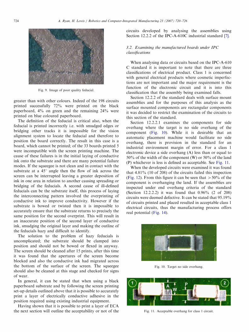
The role of the feducial of alignment target was outlinedin Section 2.3, for successful alignment of board with thestencil when screen printing the electrically conductiveadhesive it is essential that the feducial is sharp, clearlydefined and provides a good contrast with the colour of theboard material. Figs. 8 and 9 show the differences betweena successfully printed and a poorly printed feducial.From the industrial trails undertaken in this research it
can be stated that using paperboard with a black back-ground enabled the vision system to clearly identify thefeducial, as the contrast between silver and black was
ARTICLE IN PRESS
Fig. 10. Target no side overhang.
Fig. 9. Image of poor quality feducial.
Fig. 11. Acceptable overhang for class 1 circuit.
A. Ryan, H. Lewis / Robotics and Computer-Integrated Manufacturing 23 (2007) 720–726724
greater than with other colours. Indeed of the 198 circuitsprinted successfully 72% were printed on the blackpaperboard, 4% on green and the remaining 24% wereprinted on blue coloured paperboard.
The definition of the feducial is critical also, when thefeducial is printed incorrectly i.e. with smudged edges orbridging other tracks it is impossible for the visionalignment system to locate the feducial and therefore toposition the board correctly. The result in this case is aboard, which cannot be printed; of the 33 boards printed 5were incompatible with the screen printing machine. Thecause of these failures is in the initial laying of conductiveink onto the substrate and there are many potential failuremodes. If the squeegee is not clean and in contact with thesubstrate at a 451 angle then the flow of ink across thescreen can be interrupted leaving a greater deposition ofink in one area in relation to another causing spreading orbridging of the feducials. A second cause of ill-definedfeducials can be the substrate itself, this process of layingthe interconnecting pattern involved the overprinting ofconductive ink to improve conductivity. However if thesubstrate is bowed or twisted then it is impossible toaccurately ensure that the substrate returns to precisely thesame position for the second overprint. This will result inan inaccurate position of the second layer of conductiveink, smudging the original layer and making the outline ofthe feducials hazy and difficult to identify.
The solution to the problem of hazy feducials isuncomplicated; the substrate should be clamped intoposition and should not be bowed or flexed in anyway.The screen should be cleaned after 15 prints, after this timeit was found that the apertures of the screen becomeblocked and also the conductive ink had migrated acrossthe bottom of the surface of the screen. The squeegeeshould also be cleaned at this stage and checked for signsof wear.
In general, it can be stated that when using a blackpaperboard substrate and by following the screen printingset-up details outlined above that it is possible to accuratelyprint a layer of electrically conductive adhesive in theposition required using existing industrial equipment.
Having shown that it is possible to print a layer of ECAthe next section will outline the acceptability or not of the
circuits developed by analysing the assemblies usingSection 12.2.2 of the IPC-A-610C industrial standard [7].
3.2. Examining the manufactured boards under IPC
classifications
When analysing data or circuits based on the IPC-A-610C standard it is important to note that there are threeclassifications of electrical product. Class 1 is concernedwith general electrical products where cosmetic imperfec-tions are not important and the major requirement is thefunction of the electronic circuit and it is into thisclassification that the assembly being examined falls.Section 12.2.2 of the standard deals with surface mount
assemblies and for the purposes of this analysis as thesurface mounted components are rectangular componentsit was decided to restrict the examination of the circuits tothis section of the standard.Section 12.2.2.1 examines the components for side
overhang where the target is no side overhang of thecomponent (Fig. 10). While it is desirable that anautomatic placement machine would facilitate no sideoverhang, there is provision in the standard for anindustrial environment margin of error. For a class 1electronic device a side overhang (A) less than or equal to50% of the width of the component (W) or 50% of the land(P) whichever is less is defined as acceptable. See Fig. 11.When the developed circuits were examined it was found
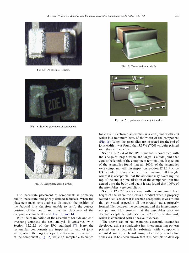
that 4.81% (10 of 208) of the circuits failed this inspection(Fig. 12). From this figure it can be seen that 450% of thecomponent is overhanging the land. If the assemblies areinspected under end overhang criteria of the standard(Section 12.2.2.2) it was found that 0.96% (2 of 208)circuits were deemed defective. It can be stated that 95.19%of circuits printed and placed resulted in acceptable class 1electrical circuits, thus the manufacturing process offersreal potential (Fig. 14).
ARTICLE IN PRESS
Fig. 12. Defect class 1 circuit.
Fig. 13. Skewed placement of component.
Fig. 14. Acceptable class 1 circuit.
Fig. 15. Target end joint width.
Fig. 16. Acceptable class 1 end joint width.
A. Ryan, H. Lewis / Robotics and Computer-Integrated Manufacturing 23 (2007) 720–726 725
The inaccurate placement of components is primarilydue to inaccurate and poorly defined feducials. When theplacement machine is unable to distinguish the position ofthe feducial it is therefore unable to verify the correctposition of the board and thus the placement of thecomponents can be skewed, Figs. 13 and 14.
With the examination of the assemblies for side and endoverhang complete the next analysis is concerned withSection 12.2.2.3 of the IPC standard [7]. Here therectangular components are inspected for end of jointwidth, where the target is a joint width equal to the widthof the component (Fig. 15) while an acceptable tolerance
for class 1 electronic assemblies is a end joint width (C)which is a minimum 50% of the width of the component(Fig. 16). When the assemblies are inspected for the end ofjoint width it was found that 3.37% (7/208) circuits printedwere deemed defective.Section 12.2.2.4 of the IPC standard is concerned with
the side joint length where the target is a side joint thatequals the length of the component termination. Inspectionof the assemblies found that all, 100% of the assemblieswere compliant with this inspection. Section 12.2.2.5 of theIPC standard is concerned with the maximum fillet heightwhere it is acceptable that the adhesive may overhang thetop of the end cap metalisation of the component but notextend onto the body and again it was found that 100% ofthe assemblies were compliant.Section 12.2.2.6 is concerned with the minimum fillet
height of the where for a class 1 product when a properlywetted fillet is evident it is deemed acceptable, it was foundthat on visual inspection all the circuits had a properlyformed fillet between the component and the interconnect-ing pattern. This ensures that the assemblies also aredeemed acceptable under section 12.2.2.7 of the standard,which is concerned with adhesive thickness.The above section has examined electronic assemblies
developed using a conductive ink interconnecting patternprinted on a degradable substrate with componentsmounted onto the board using electrically conductiveadhesives. It has been shown that it is possible to develop
ARTICLE IN PRESS
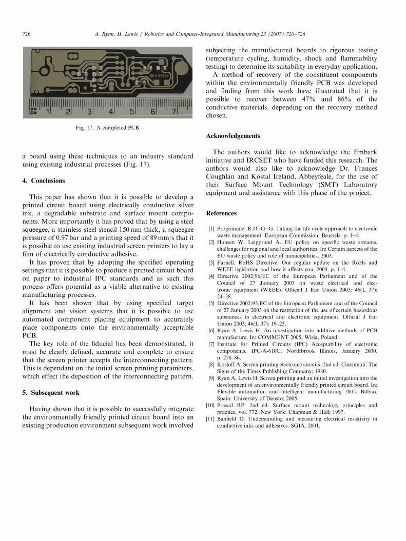
Fig. 17. A completed PCB.
A. Ryan, H. Lewis / Robotics and Computer-Integrated Manufacturing 23 (2007) 720–726726
a board using these techniques to an industry standardusing existing industrial processes (Fig. 17).
4. Conclusions
This paper has shown that it is possible to develop aprinted circuit board using electrically conductive silverink, a degradable substrate and surface mount compo-nents. More importantly it has proved that by using a steelsqueegee, a stainless steel stencil 150mm thick, a squeegeepressure of 0.97 bar and a printing speed of 89mm/s that itis possible to use existing industrial screen printers to lay afilm of electrically conductive adhesive.
It has proven that by adopting the specified operatingsettings that it is possible to produce a printed circuit boardon paper to industrial IPC standards and as such thisprocess offers potential as a viable alternative to existingmanufacturing processes.
It has been shown that by using specified targetalignment and vision systems that it is possible to useautomated component placing equipment to accuratelyplace components onto the environmentally acceptablePCB.
The key role of the fiducial has been demonstrated, itmust be clearly defined, accurate and complete to ensurethat the screen printer accepts the interconnecting pattern.This is dependant on the initial screen printing parameters,which effect the deposition of the interconnecting pattern.
5. Subsequent work
Having shown that it is possible to successfully integratethe environmentally friendly printed circuit board into anexisting production environment subsequent work involved
subjecting the manufactured boards to rigorous testing(temperature cycling, humidity, shock and flammabilitytesting) to determine its suitability in everyday application.A method of recovery of the constituent components
within the environmentally friendly PCB was developedand finding from this work have illustrated that it ispossible to recover between 47% and 86% of theconductive materials, depending on the recovery methodchosen.
Acknowledgements
The authors would like to acknowledge the Embarkinitiative and IRCSET who have funded this research. Theauthors would also like to acknowledge Dr. FrancesCoughlan and Kostal Ireland, Abbeyfeale, for the use oftheir Surface Mount Technology (SMT) Laboratoryequipment and assistance with this phase of the project.
References
[1] Programme, R.D.-G.-G. Taking the life-cycle approach to electronic
waste management. European Commission, Brussels. p. 1–4.
[2] Hansen W, Leipprand A. EU policy on specific waste streams,
challenges for regional and local authorities. In: Certain aspects of the
EU waste policy and role of municipalities, 2003.
[3] Farnell, RoHS Directive. Our regular update on the RoHs and
WEEE legislation and how it affects you. 2004. p. 1–4.
[4] Directive 2002/96/EC of the European Parliament and of the
Council of 27 January 2003 on waste electrical and elec-
tronic equipment (WEEE). Official J Eur Union 2003; 46(L 37):
24–38.
[5] Directive 2002/95/EC of the European Parliament and of the Council
of 27 January 2003 on the restriction of the use of certain hazardous
substances in electrical and electronic equipment. Official J Eur
Union 2003; 46(L 37): 19–23.
[6] Ryan A, Lewis H. An investigation into additive methods of PCB
manufacture. In: COMMENT 2005, Wisla, Poland.
[7] Institute for Printed Circuits (IPC) Acceptability of electronic
components, IPC-A-610C, Northbrook Illinois, January 2000.
p. 278–86.
[8] Kosloff A. Screen printing electronic circuits. 2nd ed. Cincinnati: The
Signs of the Times Publishing Company; 1980.
[9] Ryan A, Lewis H. Screen printing and an initial investigation into the
development of an environmentally friendly printed circuit board. In:
Flexible automation and intelligent manufacturing 2005. Bilbao,
Spain: University of Deusto; 2005.
[10] Prasad RP. 2nd ed. Surface mount technology principles and
practice, vol. 772. New York: Chapman & Hall; 1997.
[11] Banfield D. Understanding and measuring electrical resistivity in
conductive inks and adhesives. SGIA, 2001.