manual ferrari i897
DESCRIPTION
manual tecnico completoTRANSCRIPT

Detailed Service Manual Detailed Test Procedures
F 897Digital Multi-Service,
Data-Capable Portable

This Page is left Blank intentionally
897Digital Multi-Service, Data-Capable Portable
Detailed Service Manual
Detailed Test Procedures
APRIL 2010
iii6880401P59-O
Manual Revisions
Changes that occur after this manual is printed are described in the Field Manual Revisions (FMRs). The FMRs provide the most current instructions and component information.
Copyright Information
The Motorola products described in this manual may include Motorola computer programs stored in semiconductor memories or other media that are copyrighted with all rights reserved worldwide to Motorola. Laws in the United States and other countries preserve for Motorola, Inc. certain exclusive rights to the copyrighted computer programs, including the exclusive right to copy, reproduce, modify, decompile, disassemble, and reverse-engineer the Motorola computer programs in any manner or form without Motorola’s prior written consent. Furthermore, the purchase of Motorola products shall not be deemed to grant either directly or by implication, estoppels, or otherwise, any license or rights under the copyrights, patents, or patent applications of Motorola, except for a nonexclusive license to use the Motorola product and the Motorola computer programs with the Motorola product.
Trademarks
MOTOROLA, the Stylized M Logo, Message Mail, VibraCall, and iDEN are registered trademarks of Motorola, Inc. ® Reg. U.S. Pat. & Tm. Off. All other product or service names are the property of their respective owners.
© Copyright 2007, Motorola, Inc. All rights reserved.
iv 6880401P59-O
S AF E T Y AN D G E N E R AL I N F O R M AT I O N
SAFETY AND GENERAL INFORMATION
Product Operation This section contains important information on the safe and efficient operation of your mobile device. Read this information before using your integrated multi-service portable radio.* When placing or receiving a phone call, hold your radio product as you would a wire
line telephone. Speak directly into the microphone. Exposure to Radio Frequency (RF) Energy
If you wear a radio product on your body when transmitting, always place the radio product in a Motorola approved clip, holder, holster, case or body harness. If you do not use a body-worn accessory supplied or approved by Motorola and are not using the radio product in the intended use positions along side the head in the phone mode or in front of the face in the two-way radio mode—or if you hang your device from a lanyard around your neck—keep the device at least 2.5 centimeters (1 inch) from your body when transmitting.
Your phone contains a transmiter and receiver. When it is ON, it receives and transmits RF energy. When you communicate with your phone, the system handling your call controls the power level at which your phone transmits. Your Motorola phone is designed to comply with local regulatory requirements in your country concerning exposure of human beings to RF energy.
ALL MODELS WITH FCC ID IHDT56KQ1 MEET TH E G OVERN MENT’S REQUIREMENTS FOR EXPOSURE TO RADIO WAVES.
Portable Radio Product Operation and EME Exposure Your Motorola radio product is designed to comply with the following national and international standards and guidelines regarding exposure of human beings to radio frequency electromagnetic energy (EME):
Your wireless phone is a radio transmitter and receiver. It is designed and manufactured not to exceed the emission limits for exposure to radiofrequency (RF) energy set by the Federal Communications Commission of the U.S. Government. These limits are part of comprehensive guidelines and establish permitted levels of RF energy for the general population. The guidelines are based on standards that were developed by independent scientific organizations through periodic and thorough evaluation of scientific studies. The standards include a substantial safety margin designed to assure the safety of all persons, regardless of age and health.
• United States Federal Communications Commission, Code of Federal
Regulations; 47 CFR part 2 sub-part J. • American National Standards Institute (ANSI) / Institute of Electrical
and Electronics Engineers (IEEE). C95. 1-1992. • Institute of Electrical and Electronics Engineers (IEEE). C95. 1-2005
Edition.* The exposure standard for wireless mobile phones employs a unit of measurement known as the Specific Absorption Rate, or SAR. The SAR limit set by the FCC is 1.6W/kg.1 Tests for SAR are conducted using standard operating positions reviewed by the FCC with the phone transmitting at its highest certified power level in all tested frequency bands. Although the SAR is determined at the highest certified power level, the actual SAR level of the phone while operating can be well below the maximum value. This is because the phone is designed to operate at multiple power levels so as to use only the power required to reach the network. In general, the closer you are to a wireless base station antenna, the lower the power output.
• International Commission on Non-Ionizing Radiation Protection (ICNIRP) 1998.
• Ministry of Health (Canada). Safety Code 6. L i m i t s o f H u m a n E x p o s u r e t o Radiofrequency Electromagnetic Fields in the Frequency Range from 3 kHz to 300 GHz, 1999.
• Australian Communications Authority Radio communications (Electromagnetic Radiation - Human Exposure) Standard 2003.
• ANATEL, Brazil Regulatory Authority, Resolution 303 (July 2, 2002) "Regulation of the limitation of exposure to electrical, magnetic, and electromagnetic fields in the
Before a phone model is available for sale to the public, it must be tested and certified to the FCC that is does not exceed the limit established by the government-adopted requirement for safe exposure. The tests are performed in positions and locations (e.g., at the ear and worn on the body) as required by the FCC for each model. The highest SAR value for this model phone when tested for use at the ear is 0.32 W/kg and when tested on the body, as described in this user guide, is 0.45 W/kg during packet data transmission. (Body-worn measurements differ among phone models, depending upon available accessories and FCC requirements.)2
* The information provided in this document supersedes the general safety information in user’s guides published prior to May 1, 2006 radio frequency range between 9 kHz and 300 GHz." "Attachment to Resolution 303 from July 2, 2002.
While there may be differences between the SAR levels of various phones and at various positions, they all meet the government requirement for safe exposure. The FCC has granted an Equipment Authorization for this model phone with all reported SAR levels evaluated as in compliance with the FCC RF exposure guidelines. SAR information on this model phone is on file with the FCC and can be found under the Display Grant section of http://www.fcc.gov/oet/fccid after searching on FCC ID IHDT56KQ1. Additional information on Specific Absorption Rates (SAR) can be found on the Cellular Telecommunications Industry Association (CTIA) web-site at http://www.wow-com.com.
1 In the United States and Canada, the SAR limit for mobile phones used by the public is 1.6 watts/kg (W/kg) averaged over one gram of tissue. The standard incorporates a substantial margin of safety to give additional protection for the public and to account for any variations in measurements. 2 The SAR information reported to the FCC includes the FCC-accepted Motorola testing protocol, assessment procedure, and measurement uncertainty range for this product.
Operational Precautions To assure optimal radio product performance and to be sure that human exposure to RF does not exceed the guidelines set forth in the relevant standards, always follow these instructions and precautions : Two-way radio operation Your radio product has been designed and tested to comply with national and international standards and guidelines regarding human exposure to RF electromagnetic energy, when operated in the two-way mode (at the face, or at the abdomen when using an audio accessory) at usage factors of up to 50% talk/50% listen. Transmit no more than the rated duty factor of 50% of the time. To transmit (talk), push the Walkie-Talkie (WT) button. To receive calls, release the WT button. Transmitting 50% of the time or less, is important because this radio generates measurable RF energy only when transmitting (in terms of measuring for standards compliance). When using your radio product as a traditional two-way radio, hold the radio product in a vertical position with the microphone one to two inches (2.5 to 5 cm) away from the lips.
v
6880401P59-O
S AF E T Y AN D G E N E R AL I N F O R M AT I O N
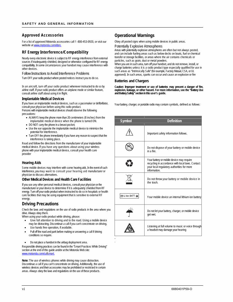
Approved Accessories For a list of approved Motorola accessories call 1 -800-453-0920, or visit our website at www.motorola.com/iden.
RF Energy Interference/Compatibility Nearly every electronic device is subject to RF energy interference from external sources if inadequately shielded, designed or otherwise configured for RF energy compatibility. In some circumstances your handset may cause interference with other devices. Follow Instructions to Avoid Interference Problems Turn OFF your radio product where posted notices instruct you to do so. In an aircraft, turn off your radio product whenever instructed to do so by airline staff. If your radio product offers an airplane mode or similar feature, consult airline staff about using it in flight.
Implantable Medical Devices If you have an implantable medical devices, such as a pacemaker or defibrillator, consult your physician before using this radio product. Persons with implantable medical devices should observe the following precautions:
• ALWAYS keep the phone more than 20 centimeters (8 inches) from the implantable medical device when the phone is turned ON.
• DO NOT carry the phone in a breast pocket; • Use the ear opposite the implantable medical device to minimize the
potential for interference. • Turn OFF the phone immediately if you have any reason to suspect that the
interference is taking place. Read and follow the directions from the manufacturer of your implantable medical device. If you have any questions about using your wireless phone with your implantable medical device, consult your health care provider Hearing Aids Some mobile devices may interfere with some hearing aids. In the event of such interference, you may want to consult your hearing aid manufacturer or physician to discuss alternatives. Other Medical Devices and Health Care Facilities If you use any other personal medical devices, consult your physician or the manufacturer or your device to determine if it is adequately shielded from RF energy. Turn off your radio product when instructed to do so in hospitals or health care facilities that may be using equipment that is sensitive to external RF energy.
Driving Precautions Check the laws and regulations on the use of radio products in the area where you drive. Always obey them. When using your radio product while driving, please: • Give full attention to driving and to the road. Using a mobile device
may be distracting. Discontinue a call if you can’t concentrate on driving. • Use hands free operation, if available. • Pull off the road and park before making or answering a call if driving
conditions so require.
• Do not place a handset in the airbag deployment area. Responsible driving practices can be found in the “Smart Practices While Driving” section at the end of this guide and/or at the Motorola Web site: www.motorola.com/callsmart. Note: The use of wireless phones while driving may cause distraction.
Operational Warnings Obey all posted signs when using mobile devices in public areas. Potentially Explosive Atmospheres Areas with potentially explosive atmospheres are often but not always posted, and can include fueling areas such as below decks on boats, fuel or chemical transfer or storage facilities, or areas where the air contains chemicals or particles, such as grain, dust or metal powders. When you are in such area, turn off your handset, and do not remove, install, or charge batteries unless it is a radio product type especially qualified for use in such areas as “Intrinsically Safe” (for example, Factory Mutual, CSA, or UL approved). In such areas, sparks can occur and cause an explosion or fire
Batteries and Chargers Caution: Improper treatment or use of batteries may present a danger of fire, explosion, leakage, or other hazard. For more information, see the “Battery Use and Battery Safety” section in this user’s guide. Your battery, charger, or portable radio may contain symbols, defined as follows:
Symbol Definition
Important safety information follows.
Do not dispose of your battery or mobile device in a fire.
Your battery or mobile device may require recycling in accordance with local laws. Contact your local regulatory authorities for more information.
Do not throw your battery or mobile device in the trash.
Your mobile device an internal lithium ion battery
Do not let your battery, charger, or mobile device get wet.
Listening at full volume to music or voice through a headset may damage your hearing
.
.
Discontinue a call if you can’t concentrate on driving. Additionally, the use of wireless devices and their accessories may be prohibited or restricted in certain areas. Always obey the laws and regulations on the use of these products.
vi 6880401P59-O
S AF E T Y AN D G E N E R AL I N F O R M AT I O N
Choking Hazards Your portable radio or its accessories may include detachable parts, which may present a choking hazard to small children. Keep your device and its accessories away from small children. Glass Parts Some parts of your mobile device may be made of glass. This glass could break if the product is dropped on a hard surface or receives a substantial impact. If glass breaks, do not touch or attempt to remove. Stop using your mobile device until the glass is replaced by a qualified service center. Seizures/Blackouts Some people may be susceptible to epileptic seizures or blackouts when exposed to flashing lights, such as when playing video games. These may occur even if a person has never had a previous seizure or blackout
If you have experienced seizures or blackouts, or if you have a family history of such occurrences, please consult with your physician before playing video games or enabling a flashing-lights feature (if available) on your mobile device. Discontinue use and consult a physician if any of the following symptoms occur: convulsion, eye or muscle twitching, loss of awareness, involuntary movements, or disorientation. It is always a good idea to hold the screen away from your eyes, leave the lights on in the room, take a 15-minute break every hour, and stop use if you are very tired.
Caution About High Volume Usage Listening at full volume to music or voice through a headset may damage your hearing.
Repetitive Motion When you repetitively perform actions such as pressing keys or entering finger-written characters, you may experience occasional discomfort in your hands, arms, shoulders, neck, or other parts of your body. If you continue to have discomfort during or after such use, stop use and see a physician. Service & Repairs If you have questions or need assistance, we’re here to help. Go to www.motorola.com/iden/support, where you can select from a number of customer care options. You can also contact the Motorola Customer Support Center at 1 -800-453-0920 (United States), 1-877-483-2840 (TTY/TDD United States for hearing impaired)
vii6880401P59-O
S AF E T Y AN D G E N E R AL I N F O R M AT I O N
Charging precautions: When charging your battery, keep it near room temperature. Never expose batteries to temperatures below 0°C (32°F) or above 45°C (113°F) when charging. Always take your mobile device with you when you leave your vehicle
Battery Use & Battery Safety • Motorola recommends you always use
Motorola-branded batteries and chargers. The warranty does not cover damage caused by non-Motorola batteries and/or chargers. Caution: Use of an unqualified battery or charger may present a risk of fire, explosion, leakage, or other hazard. Improper battery use, or use of a damaged battery, may result in a fire, explosion, or other hazard.
• When storing your battery, keep it in a cool, dry place.
• Battery usage by children should be supervised.
• Important: Motorola mobile devices are designed to work best with qualified batteries. If you see a message on your display such as Invalid Battery or Unable to Charge, take the following steps:
• Remove the battery and inspect it to confirm that it bears a Motorola “Original Equipment” hologram;
• If there is no hologram, the battery is not a qualified battery;
• If there is a hologram, replace the battery and retry charging it;
• If the message remains, contact a Motorola Authorized Service Center.
• New batteries or batteries stored for a long time may take more time to charge.
• It is normal over time for battery life to decrease, and for the battery to exhibit shorter runtime between charges or require more frequent or longer charging times.
• Avoid damage to battery and mobile device. Do not disassemble, open, crush, bend, deform, puncture, shred, or submerge the battery or mobile device. Avoid dropping the battery or mobile device, especially on a hard surface. If your battery or mobile device has been subjected to such damage, take it to a Motorola
Authorized Service Center before using. Do not attempt to dry it with an appliance or heat source, such as a hair dryer or microwave oven.
• Use care when handling a charged battery—particularly when placing it inside a pocket, purse, or other container with metal objects. Contact with metal objects (e.g., jewelry, keys, beaded chains) could complete an electrical circuit (short circuit), causing the battery to become very hot, which could cause damage or injury.
Promptly dispose of used batteries in accordance with local regulations.
Contact your local recycling center for proper battery disposal.
Warning: Never dispose of batteries in a fire because they may explode.
viii 6880401P59-O
M O D E L I N F O R M A T I O N
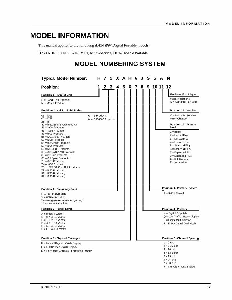
MODEL INFORMATION This manual applies to the following iDEN i897 Digital Portable models:
H75XAH6JS5AN 806-940 MHz, Multi-Service, Data-Capable Portable
MODEL NUMBERING SYSTEM Typical Model Number: H 7 5 X A H 6 J S 5 A N
Position: 1
ix
2 3 4 5 6 7 8 9 10 11 12
Position 1 - Type of Unit
Position 12 - Unique
H = Hand-Held Portable M = Mobile Product
Model Variations N = Standard Package
Positions 2 and 3 - Model Series
Position 11 - Version
Version Letter (Alpha) Major Change
Position 10 - Feature level
01 = i365 02 = i776 23 = i9 40 = i85s/i55sr/i50sx Products 41 = i90c Products 45 = i265 Products 48 = i80s Products 56 = i30sx/i30s Products 57 = i95cl Products 58 = i88s/i58sr Products 59 = i60c Products 62 = i205/i305 Products 63 = i530/i730/i710 Products 68 = i325pro Products 69 = i31 5plus Products 73 = i860 Products 74 = i830 Products 75 = i285 / i890 / i897 Products 72 = i930 Products 85 = i870 Products ; 83 = i580 Products ;
92 = i9 Products 94 = i880/i885 Products
1 = Basic 2 = Limited Pkg 3 = Limited Plus 4 = Intermediate 5 = Standard Pkg 6 = Standard Plus 7 = Expanded Pkg 8 = Expanded Plus
9 = Full Feature Programmable
Position 4 - Frequency Band Position 9 - Primary System T
R = iDEN Shared U = 806 to 870 MHz
X = 806 to 941 MHz *Values given represent range only; they are not absolute.
Position 5 - Power Level Position 8 - Primary N = Digital Dispatch A = 0 to 0.7 Watts
Q = Low Profile - Basic DisplayB = 0.7 to 0.9 Watts R = Digital Multi-Service C = 1.0 to 3.9 Watts
D = 4.0 to 5.0 Watts J = TDMA Digital Dual Mode E = 5.1 to 6.0 Watts F = 6.1 to 10.0 Watts
Position 6 - Physical Packages Position 7 - Channel Spacing
1 = 5 kHz 2 = 6.25 kHz 3 = 10 kHz 4 = 12.5 kHz
F = Limited Keypad - With Display H = Full Keypad - With Display N = Enhanced Controls - Enhanced Display
5 = 15 kHz 6 = 25 kHz 7 = 30 kHz 9 = Variable Programmable
6880401P59-O
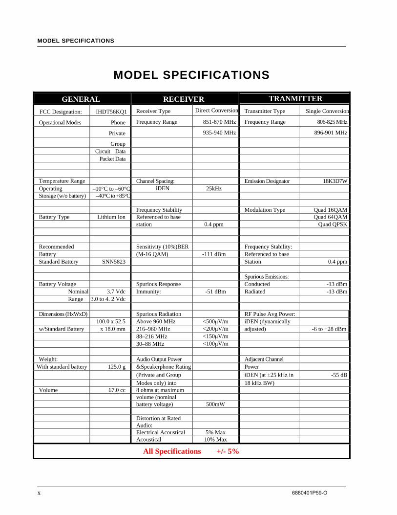
MODEL SPECIFICATIONS
MODEL SPECIFICATIONS
GENERAL RECEIVER TRANMITTER
FCC Designation: IHDT56KQ1 Receiver Type Direct Conversion Transmitter Type Single Conversion
Operational Modes Phone Frequency Range 851-870 MHz Frequency Range 806-825 MHz
Private 935-940 MHz 896-901 MHz
Group Circuit Data Packet Data Temperature Range Channel Spacing: Emission Designator 18K3D7WOperating –10°C to –60°C iDEN 25kHz Storage (w/o battery) –40°C to +85°C Frequency Stability Modulation Type Quad 16QAMBattery Type Lithium Ion Referenced to base Quad 64QAM station 0.4 ppm Quad QPSK Recommended Sensitivity (10%)BER Frequency Stability: Battery (M-16 QAM) -111 dBm Referenced to base Standard Battery SNN5823 Station 0.4 ppm Spurious Emissions: Battery Voltage Spurious Response Conducted -13 dBm Nominal 3.7 Vdc Immunity: -51 dBm Radiated -13 dBm Range 3.0 to 4. 2 Vdc Dimensions (HxWxD) Spurious Radiation RF Pulse Avg Power: 100.0 x 52.5 Above 960 MHz <500μV/m iDEN (dynamically w/Standard Battery x 18.0 mm 216–960 MHz <200μV/m adjusted) -6 to +28 dBm 88–216 MHz <150μV/m 30–88 MHz <100μV/m Weight: Audio Output Power Adjacent Channel
With standard battery 125.0 g &Speakerphone Rating Power (Private and Group iDEN (at ±25 kHz in -55 dB
Modes only) into 18 kHz BW) Volume 67.0 cc 8 ohms at maximum volume (nominal battery voltage) 500mW Distortion at Rated Audio: Electrical Acoustical 5% Max
Acoustical 10% Max
All Specifications +/- 5%
x 6880401P59-O
PREFACE: Conventions Used in This Manual
PREFACE
The i897 is Digital Multi-Service, Data-Capable Portable Field Service Manual contains the information necessary to identify and fix problems in the Motorola i897 is Digital Portable. This unit is based on digital technology and is designed to operate on iDEN systems.
Basic and field-level service for this unit as described in this manual includes troubleshooting, testing, board swapping, and maintenance.
Service for this unit is based on the substitution method: a faulty part is replaced by a working one, providing quicker service to the customer. For example, if the battery is faulty, it is replaced. If the unit requires more complete testing or service than is available at the basic level, it is sent to the field-level service facility, serviced, and returned to the iDEN Customer Care Center (ICC).
NOTE: Before operating or testing this unit, please read the Safety and General Information section in the front of this manual.
Who Should Use This Manual This manual is intended for service technicians who should be familiar with the test equipment recommended in Appendix A. To help pinpoint basic problems with the unit, first perform the mechanical checks and self tests as described in Chapter 5; then proceed to field level troubleshooting and testing.
How This Manual Is Organized This manual contains the following chapters and appendices: Chapter 1 presents the theory and technology used by the iDEN system and unit.
Chapter 2 describes how to prepare test equipment setups for the iDEN system and how to operate the test equipment. It also contains disassembly and reassembly instructions.
Chapter 3 describes the troubleshooting procedures. Chapter 4 contains the component board layouts, schematic diagrams and component lists.
Appendix A Provides information on ordering kits and replacement parts. It also contains lists of recommended test equipment.
xi6880401P59-O
PREFACE: Conventions Used in This Manual
Conventions Used in This Manual The following conventions are used throughout this manual:
italics Used for emphasis and new terms b o l d Defines menu items, fields, and buttons c o d e Used for sample input and output
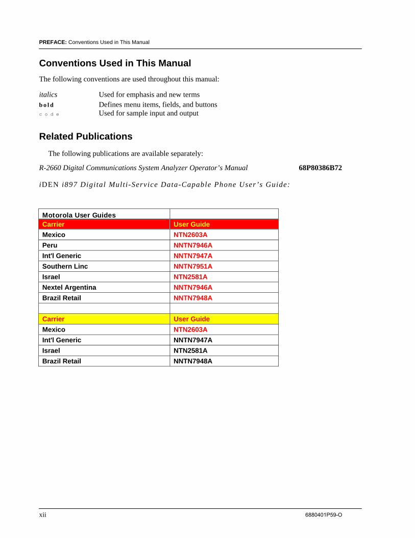
Related Publications The following publications are available separately:
R-2660 Digital Communications System Analyzer Operator’s Manual 68P80386B72
iDEN i897 Digital Multi-Service Data-Capable Phone User’s Guide:
Motorola User Guides Carrier User Guide Mexico NTN2603A Peru NNTN7946A Int'l Generic NNTN7947A Southern Linc NNTN7951A Israel NTN2581A Nextel Argentina NNTN7946A Brazil Retail NNTN7948A Carrier User Guide Mexico NTN2603A Int'l Generic NNTN7947A Israel NTN2581A Brazil Retail NNTN7948A
xii 6880401P59-O
CONTENTS
SAFETY AND GENERAL INFORMATION............................................v
MODEL INFORMATION...............................................................................ix
MODEL SPECIFICATIONS ......................................................................x
PREFACE ...................................................................................................xi CONTENTS ................................................................................................xiii Chapter 1 ....................................................................................................17
SYSTEM OVERVIEW ..................................................................................17 1.1 iDEN Digital Modulation Technology......................................................................................... 17 1.2 iDEN Voice Compression Technology ........................................................................................ 19
1.2.1 RF Transmission Bursts ......................................................................................................................... 19 1.2.2 Calling Area Coverage........................................................................................................................... 20 1.2.3 Service Area........................................................................................................................................... 21
1.3 Radio Architecture Overview ...................................................................................................... 22 1.4 Roadrunner Circuitry .................................................................................................................. 23 1.5 Audio Section ............................................................................................................................... 25
1.5.1 Acoustic Transducers............................................................................................................................. 25 1.5.2 Audio Amplifiers ................................................................................................................................... 25 1.5.3 Audio Modes.......................................................................................................................................... 27 1.5.4 Audio Paths............................................................................................................................................ 27 1.5.5 Transmit Paths ....................................................................................................................................... 28 1.5.6 Receive Paths......................................................................................................................................... 28
1.6 Digital Section ............................................................................................................................... 28 1.6.1 Zeus Processor ....................................................................................................................................... 29 1.6.2 MCU Digital Phase Locked Loop (DPLL) ............................................................................................ 30 1.6.3 Host System Clock Synthesizer ............................................................................................................. 30 1.6.4 Host System Clock Synthesizer ............................................................................................................. 30 1.6.5 ZEUS Digital Signal Processor.............................................................................................................. 31 1.6.6 DSP Phase Locked Loop (PLL)............................................................................................................. 31 1.6.7 Serial Peripheral Interface (SPI) ............................................................................................................ 31 1.6.8 System Memory..................................................................................................................................... 32 1.6.9 USB2.0................................................................................................................................................... 32 1.6.10 Battery ID .............................................................................................................................................. 33 1.6.11 Keypad Block ........................................................................................................................................ 33 1.6.12 LCD Circuit ........................................................................................................................................... 34 1.6.13 CMOS 2.0 Mega-pixel Focus Camera ................................................................................................... 34
1.7 Transmitter Path Section ............................................................................................................. 35 1.7.1 ROADRUNNER.................................................................................................................................... 36 1.7.2 Sledgehammer IC (TX Path).................................................................................................................. 37 1.7.3 JANUS................................................................................................................................................... 37 1.7.4 Cartesian Feedback ................................................................................................................................ 39 1.7.5 Level Set and Phase Training................................................................................................................. 40
xiii6880401P59-O
1.8 Receiver Path Section................................................................................................................... 42 1.8.1 JANUS Module (RXPath) ......................................................................................................................43 1.8.2 Sledgehammer IC (RXPath)...................................................................................................................43 1.8.3 Roadrunner IC (RX Path) .......................................................................................................................43
1.9 Frequency Generator (RF) Section............................................................................................. 44 1.10 Global Positioning System (GPS) Section ............................................................................... 45
1.10.1 GPS Receiver .........................................................................................................................................45 1.10.2 GPS Antenna ..........................................................................................................................................46 1.10.3 JANUS IC...............................................................................................................................................46 1.10.4 GPS Receiver .........................................................................................................................................46 1.10.5 GPS Receiver .........................................................................................................................................46 1.10.6 GPS Receiver .........................................................................................................................................46 1.10.7 GPS Receiver .........................................................................................................................................46 1.10.8 GPS Receiver .........................................................................................................................................46
1.11 Bluetooth® Wireless System .................................................................................................... 47
Chapter 2 ................................................................................................... 49
PREPARING FOR FIELD LEVEL TESTING .............................................. 49 2.1 Preparing Equipment for Testing ............................................................................................... 49
2.1.1 Calibrating Equipment............................................................................................................................49 2.1.2 Checking the RF Cable...........................................................................................................................49 2.1.3 Strong-Signal Environments...................................................................................................................49 2.1.4 Protecting Static-Sensitive Devices........................................................................................................49
2.2 Using RSS ...................................................................................................................................... 50 2.3 Connecting an i897 Unit to the R-2660 ....................................................................................... 50 2.4 Operating the R-2660 ................................................................................................................... 51 2.5 Dis-Assembly and Assembly of i897 Unit ................................................................................... 52 2.6 Disassembly Procedure ................................................................................................................ 52
2.6.1 Disassembly Sequence Pane chart..........................................................................................................52 2.6.2 Battery Cover and Battery Removal.......................................................................................................53 2.6.3 SIM Card and SD Card Removal ...........................................................................................................54 2.6.4 Back Housing Removal ..........................................................................................................................55 2.6.5 Main Board Removal .............................................................................................................................56 2.6.6 Flip Assembly Access ............................................................................................................................57
2.7 Assembly Procedure ..................................................................................................................... 59 2.7.1 Assembly Sequence Pane Chart .............................................................................................................59 2.7.2 Main Board Preparation .........................................................................................................................60 2.7.3 Flip to Front Housing Assembly ............................................................................................................62 2.7.4 Main Board Assembly............................................................................................................................65 2.7.5 Back Housing Assembly ........................................................................................................................67 2.7.6 Closing the Unit......................................................................................................................................68 2.7.7 SIM Card and SD Card Installation........................................................................................................69 2.7.8 Battery and Battery Door Installation.....................................................................................................70
Chapter 3 .................................................................................................... 71
TROUBLESHOOTING ............................................................................. 71 3.1 Digital Analysis Test ..................................................................................................................... 71
xiv 6880401P59-O
3.2 LO Output Test............................................................................................................................. 74 3.3 RX Main VCO Test ...................................................................................................................... 75 3.4 Keypad Failure Test. .................................................................................................................... 77 3.5 SLEDGEHAMMER Test............................................................................................................. 78 3.6 RX Analysis Test ........................................................................................................................... 80 3.7 TX Power Test............................................................................................................................... 83 3.8 Tx Janus Module Test .................................................................................................................. 84 3.9 SLEDGEHAMMER Tx Test ....................................................................................................... 86 3.10 Earpiece Speaker Test .............................................................................................................. 89 3.11 High Audio Speaker Test.......................................................................................................... 91 3.12 Audio Loopback Level Test...................................................................................................... 93 3.13 Reference Oscillator Test.......................................................................................................... 94 3.14 DC Distribution (V1) Test ........................................................................................................ 96 3.15 DC Distribution (V2) Test ........................................................................................................ 97 3.16 DC Distribution (V3) Test ........................................................................................................ 98 3.17 DC Distribution (V4) Test ........................................................................................................ 99 3.18 DC Distribution (V_VIB) Test ............................................................................................... 100 3.19 DC Distribution (SW1) Test ................................................................................................... 101 3.20 DC Distribution (SW2) Test ................................................................................................... 102 3.21 DC Distribution (SW3) Test ................................................................................................... 103 3.22 DC Distribution (VUSB) Test................................................................................................. 104 3.23 DC Distribution (VSIM) Test................................................................................................. 105 3.24 DC Distribution (VHOLD) Test............................................................................................. 106 3.25 GPS Receiver Test................................................................................................................... 107 3.26 Mototalk ................................................................................................................................... 110 3.27 Model Assembly (MA) Test Mode Test................................................................................. 110
Chapter 4 ..................................................................................................115 4.1 Main Board Component Layout................................................................................................ 116 4.2 HIERARCHY - TOP SHEET.................................................................................................... 117 4.3 ZEUS DIGITAL INTERFACE ................................................................................................. 118 4.4 ZEUS MEMORY INTERFACE ............................................................................................... 119 4.5 ZEUS POWER............................................................................................................................ 120 4.6 DISPLAY AND CAMERA INTERFACE................................................................................ 121 4.7 ZEUS............................................................................................................................................ 122
xv6880401P59-O
4.8 KEYPAD B2B CONNECTOR .................................................................................................. 123 4.9 ROADRUNNER DC................................................................................................................... 124 4.10 ROADRUNNER INTERFACE ............................................................................................. 125 4.11 ROADRUNNER AUDIO ....................................................................................................... 126 4.12 ROADRUNNER RF INTERFACE - EMU .......................................................................... 127 4.13 BLUETOOTH ......................................................................................................................... 128 4.14 EMU BLOCK.......................................................................................................................... 129 4.15 EMU IC.................................................................................................................................... 130 4.16 TRANSCEIVER...................................................................................................................... 131 4.17 Component Locations ............................................................................................................. 132
APPENDIX A .......................................................................................... 141 A.1 Customer Service ............................................................................................................................ 141 A.2 Replacement Parts .......................................................................................................................... 141 A.3 Domestic Orders ............................................................................................................................. 141 A.4 International Orders ...................................................................................................................... 141 A.5 Replacement Kits ............................................................................................................................ 142 A.6 Recommended Test Equipment and Tools................................................................................... 145 A.7 Recommended Programming Equipment .................................................................................... 146
xvi 6880401P59-O
OVERVIEW: iDEN Digital Modulation Technology
Chapter 1 SYSTEM OVERVIEW
To achieve a high spectrum efficiency, the i897 digital multi-service, data-capable portable unit uses a unique modulation technology and sophisticated voice-compression algorithm. The voice of the person speaking into the microphone is converted into a digital bit stream consisting of zeros (0) and ones (1). The stream then is modulated into a radio-frequency (RF) signal, which is transmitted over the air to another unit. This process is called digital modulation.
1.1 iDEN Digital Modulation Technology
The i897 digital portable is a dual band 806-870 MHz and 896-940 MHz unit. It operates in multiple modes: phone, private, data, and group; and uses three digital modulation technologies: Quad QAM, Quadrature Phase Shift Keying (QPSK), and Time Division Multiple Access (TDMA).
Quadrature Amplitude Modulation (QAM) is a modulation technique that transmits information by altering the amplitude and phase of the radio frequency (RF) signal. Data is converted into complex symbols, which alter the RF signal and transmit the information. When the signal is received, the amplitude and phase are converted back into symbols and then into the original data.
There are three different QAM modes that are used for different applications: 64QAM, 16QAM, and 4QAM. In voice applications, 16QAM is used, while in data applications, 64QAM, 16QAM, and 4QAM are used.
NOTE: The 900 MHz band operates only in 16QAM modulation.
In 64QAM, 64 possible combinations of 6 bits are converted into a unique amplitude and phase. In 16QAM, there are 16 possible combinations of 4 bits, while in 4QAM, there are 4 possible combinations of 2 bits.
The traditional 25 kHz channel used for two-way radios is split into four QAM signals (subcarriers) that are transmitted simultaneously. This technique can transmit 64 Kbps in a single 25 kHz channel
The iDEN system requires approximately 10 Kbps to transmit a compressed voice; therefore, 64 Kbps can accommodate 6 voice channels or 3 voice channels in enhanced systems.
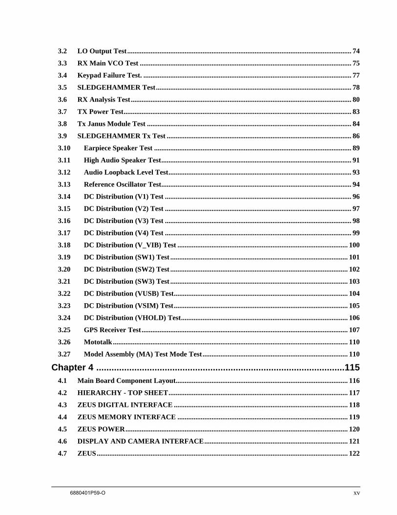
The signal spectrum of the Quad 16QAM is shown in Figure 1-1
6880401P59-O 17
OVERVIEW: iDEN Digital Modulation Technology
Frequency from Desired Channel Center (kHz)
Figure 1-1: Spectrum of iDEN Quad 16QAM
Quadrature Phase Shift Keying (QPSK) is one of the most common modulation techniques for satellite communications. In QPSK, a digital data stream is taken two bits at a time to generate four possible phase states of the transmitted carrier. A characteristic of this technique is its resistance to noise.
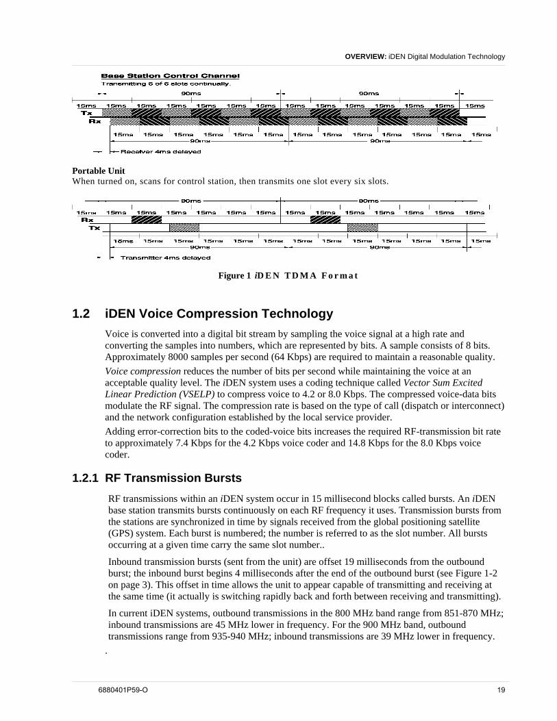
Time Division Multiple Access (TDMA) is used to allocate portions of the RF signal by dividing time into 6 slots, one for each unit. Time allocation enables each unit to transmit its voice information without interference from another unit’s transmission.
Transmission from a unit or base station is accommodated in time-slot lengths of 15 milliseconds and frame lengths of 90 milliseconds (see Figure 1-2).
Note that Rx (outbound) indicates base-to subscriber transmissions; Tx (inbound) indicates subscriber-to-base transmissions. The slots are paired and have a fixed offset of 19 milliseconds; their timings are synchronized by the iDEN system. The TDMA technique requires sophisticated algorithms and one digital-signal processor (DSP) to perform voice compression/decompression and RF modulation/demodulation
18 6880401P59-O
OVERVIEW: iDEN Digital Modulation Technology
Portable Unit When turned on, scans for control station, then transmits one slot every six slots.
Figure 1 iD E N T D M A F o r m a t
1.2 iDEN Voice Compression Technology Voice is converted into a digital bit stream by sampling the voice signal at a high rate and converting the samples into numbers, which are represented by bits. A sample consists of 8 bits. Approximately 8000 samples per second (64 Kbps) are required to maintain a reasonable quality. Voice compression reduces the number of bits per second while maintaining the voice at an acceptable quality level. The iDEN system uses a coding technique called Vector Sum Excited Linear Prediction (VSELP) to compress voice to 4.2 or 8.0 Kbps. The compressed voice-data bits modulate the RF signal. The compression rate is based on the type of call (dispatch or interconnect) and the network configuration established by the local service provider. Adding error-correction bits to the coded-voice bits increases the required RF-transmission bit rate to approximately 7.4 Kbps for the 4.2 Kbps voice coder and 14.8 Kbps for the 8.0 Kbps voice coder.
1.2.1 RF Transmission Bursts RF transmissions within an iDEN system occur in 15 millisecond blocks called bursts. An iDEN base station transmits bursts continuously on each RF frequency it uses. Transmission bursts from the stations are synchronized in time by signals received from the global positioning satellite (GPS) system. Each burst is numbered; the number is referred to as the slot number. All bursts occurring at a given time carry the same slot number..
Inbound transmission bursts (sent from the unit) are offset 19 milliseconds from the outbound burst; the inbound burst begins 4 milliseconds after the end of the outbound burst (see Figure 1-2 on page 3). This offset in time allows the unit to appear capable of transmitting and receiving at the same time (it actually is switching rapidly back and forth between receiving and transmitting).
In current iDEN systems, outbound transmissions in the 800 MHz band range from 851-870 MHz; inbound transmissions are 45 MHz lower in frequency. For the 900 MHz band, outbound transmissions range from 935-940 MHz; inbound transmissions are 39 MHz lower in frequency.
.
6880401P59-O 19
OVERVIEW: iDEN Digital Modulation Technology
An iDEN channel is created by grouping bursts so that their slot numbers differ by a number referred to as the repetition rate. The i897 unit uses two repetition rates for interconnect voice calls: 6:1 and 3:1. A single frequency can handle six calls using a 6:1 repetition rate with the 4.2 Kbps coder. Dispatch calls always use this rate. However, the audio quality of the 3:1 repetition rate with the 8.0 Kbps coder is superior to the 6:1 rate with the 4.2 Kbps coder. Most service providers configure the system and unit to allow only the 3:1 rate for interconnect calls. Calls are set up on a primary control channel (PCCH) in response to a request from a unit or a regular telephone connected to the Public Switch Telephone Network (PSTN). The PCCH is established by the base station equipment; typically, it is a 6:1 channel. The outbound PCCH carries system information and “pages” to specific subscriber units and asks them to respond if they are available for a call. Inbound PCCH transmissions carry responses to the “pages” and requests by subscriber units to set up calls. Inbound transmissions on the primary control channel only take 7.5 milliseconds and can be timed to occur in either half of a 15- millisecond burst. The dual band unit will power up in the 800 MHz band and will use these channels for control channels—Primary Control Channel (PCCH) and Broadcast Control Channel (BCCH). The 900 MHz mode will be used only during 3:1 interconnect calls. Every attempt will be made to assign the unit to 900 MHz carriers during new 3:1 interconnect calls, handovers into a cell, and inter-cell handovers. If no resources are available, or if available resources have insufficient channel quality (in the case of a handover), then 800 MHz carriers will be evaluated. Using the above techniques, the iDEN system can operate six voice channels simultaneously in dispatch mode or 3 voice channels simultaneously in interconnect mode on a single RF carrier at 25 kHz bandwidth
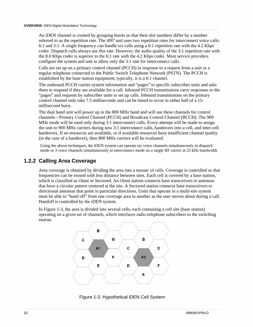
1.2.2 Calling Area Coverage Area coverage is obtained by dividing the area into a mosaic of cells. Coverage is controlled so that frequencies can be reused with less distance between sites. Each cell is covered by a base station, which is classified as Omni or Sectored. An Omni station connects base transceivers to antennas that have a circular pattern centered at the site. A Sectored station connects base transceivers to directional antennas that point in particular directions. Units that operate in a multi-site system must be able to “hand off” from one coverage area to another as the user moves about during a call. Handoff is controlled by the iDEN system.
In Figure 1-3, the area is divided into several cells, each containing a cell site (base station) operating on a given set of channels, which interfaces radio-telephone subscribers to the switching station.
Figure 1-3. Hypothetical iDEN Cell System
20 6880401P59-O
OVERVIEW: iDEN Digital Modulation Technology
The units are capable of operation on any channel in the system. This enables them to operate in any cell. Due to the low power requirements for communications between radio telephones in a particular cell and cell site, operating channels may be repeated in cells that are outside the coverage area of each other.
For example, in Figure 1-3, each letter represents a given frequency. Notice that cells A1 and A2 operate on the same frequency because they are a certain distance apart. Users can simultaneously occupy the same frequency without interfering with each other. This is known as frequency re-use.
The implementation of frequency re-use increases the cell handling capability of the system without increasing the number of available channels. When re-using identical frequencies in a small area, co-channel interference can be a problem. The iDEN system can tolerate higher levels of co-channel interference than analog systems by incorporating digital modulation. This means that cells using identical frequencies can be physically closer than similar cells in analog systems. Therefore, the advantage of frequency re-use can be further enhanced in an iDEN system, enabling greater traffic handling in high-use areas.
Because of TDMA, several calls can share the same carrier. The carrier is divided into a continuous stream of TDMA frames, each of which is split into six time slots (see Figure 1-2 on page 3). When a connection is required, the system allocates the subscriber a dedicated time slot within each TDMA frame. User data (speech or data) for transmission is digitized and sectioned into blocks. The user data blocks are sent as information bursts in the allocated time slot of each TDMA frame. The data blocks are modulated onto the carrier via M16 QAM.
Each unit must be able to move from one cell to another with no detection by the user. The unit itself carries out signal-strength measurements on adjacent cells, and the quality of the traffic channel is measured by both the unit and the base station. The hand-over criteria can be much more accurately determined, and the hand-over made before the channel quality deteriorates to a level that the subscriber can notice.
When a unit is well within a cell, the signal strength measured will be high. As the unit moves toward the edge of the cell, the signal strength and quality measurement decreases.
Signal information provides an indication of the subscriber's distance from the base station. As the unit moves from cell to cell, its control is handed from one base station to another. The change is handled by the unit and the base station, and is completely transparent to the user.
1.2.3 Service Area Because this is a radio system, there are no exact boundaries that can be drawn on a map. If the unit is outside the coverage area, “No Service” illuminates on the display and calls are unable to be placed or received. If this happens during a conversation, the call will be lost. There also may be small areas within a particular service area in which communications could be lost.
The unit’s identity information is held by its local iDEN system in its Home Location Register (HLR) and Visitor Location Register (VLR). The VLR contains identity information on all local active radio telephones. Should the user roam to another area, the unit’s identity information is sent to the VLR in the new system. The new system will then check the unit's details with the home system for authenticity. If everything is in order, the user will be able to initiate and receive calls while in the new area.
6880401P59-O 21
OVERVIEW: iDEN Digital Modulation Technology
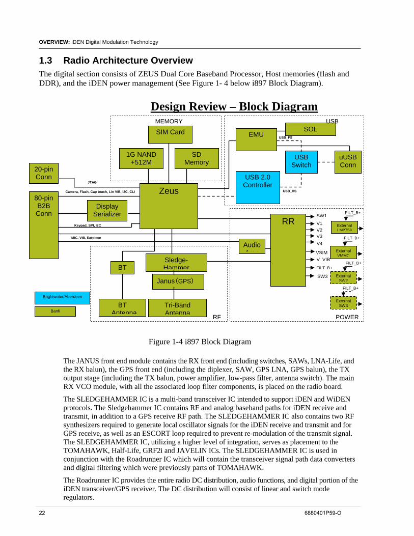
1.3 Radio Architecture Overview The digital section consists of ZEUS Dual Core Baseband Processor, Host memories (flash and DDR), and the iDEN power management (See Figure 1- 4 below i897 Block Diagram).
Design Review – Block Diagram
Zeus
BT
BT Antenna
Sledge- Hammer
Janus(GPS)
Tri-Band Antenna
USB 2.0 Controller
USB Switch uUSB
Conn
EMUSOL
SD Memory
SIM Card
1G NAND +512M
20-pin Conn
Display Serializer
External SW2
FILT_B+
External VMMC
FILT_B+
External SW3
FILT_B+
80-pin B2B Conn
POWERRF
MEMORY USB
RR SW1V1 V2 V3
VSIM V_VIB
FILT_B+
JTAG Camera, Flash, Cap touch, Lin VIB, I2C, CLI
Keypad, SPI, I2C MIC, VIB, Earpiece
USB_HS
USB_FS
Brightwater/Aberdeen Banfi
Audio Amp
V4
SW3
External LM2758
FILT_B+
Figure 1-4 i897 Block Diagram
The JANUS front end module contains the RX front end (including switches, SAWs, LNA-Life, and the RX balun), the GPS front end (including the diplexer, SAW, GPS LNA, GPS balun), the TX output stage (including the TX balun, power amplifier, low-pass filter, antenna switch). The main RX VCO module, with all the associated loop filter components, is placed on the radio board.
The SLEDGEHAMMER IC is a multi-band transceiver IC intended to support iDEN and WiDEN protocols. The Sledgehammer IC contains RF and analog baseband paths for iDEN receive and transmit, in addition to a GPS receive RF path. The SLEDGEHAMMER IC also contains two RF synthesizers required to generate local oscillator signals for the iDEN receive and transmit and for GPS receive, as well as an ESCORT loop required to prevent re-modulation of the transmit signal. The SLEDGEHAMMER IC, utilizing a higher level of integration, serves as placement to the TOMAHAWK, Half-Life, GRF2i and JAVELIN ICs. The SLEDGEHAMMER IC is used in conjunction with the Roadrunner IC which will contain the transceiver signal path data converters and digital filtering which were previously parts of TOMAHAWK.
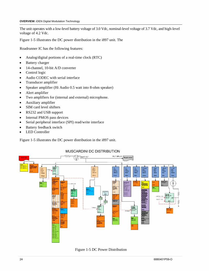
The Roadrunner IC provides the entire radio DC distribution, audio functions, and digital portion of the iDEN transceiver/GPS receiver. The DC distribution will consist of linear and switch mode regulators.
22 6880401P59-O
OVERVIEW: iDEN Digital Modulation Technology
The audio section is composed of microphone amplifiers, speaker amplifiers, a voice codec and a stereo DAC. Previously such functionality was performed with the GCAP/PCAP IC. The receiver ROADRUNNER portion includes circuitry supporting AGC, receiver sequence management, signal path anti-aliasing filters, buffer amplifiers, high dynamic range sigma delta data converters, digital filtering and the RX serial data interface to the baseband processor (previously part of Tomahawk). The TX portion includes circuitry supporting Pulse Shaping FIR, TX DAC, Smoothing filters, PA Gain Control DAC, and the TX serial data interface to the baseband processor (previously part of TOMAHAWK). ROADRUNNER also includes circuitry to support additional features such as GPS AD, USB, RS232, LEDs, etc.
Finally, the baseband processor utilized by i897 is the Zeus Processor.
1.4 Roadrunner Circuitry
The Roadrunner integrated circuit (IC) provides the following:
• DC distribution • Audio CODEC and amplifiers • Control logic for power on/off • A/D converters for monitoring radio thermistors, battery level, LCD calibration, and the
Photosensor. • The Roadrunner IC used is a 223 I/O MAP BGA package.
The i897 unit has the following DC distribution:
• SW1 is a BUCK step-down switching regulator set to 1.2 Vdc at 550 mA. It supplies the Zeus core. • SW2 is an external BUCK switching regulator set to 1.875Vdc at 600mA.. • SW3 is a BOOST switching regulator set to 5.6 Vdc at 200 mA. It supplies Vusb. • V1-The V1_LDO (2.775Vdc at 200mA) is used to power the camera, LCD and photo sensor in a
Zeus-based platform • V2 - 2.775 Vdc at 350 mA - will be used to power most of the RF circuits as well as the audio codec
and all audio amps. • SW3 is a BOOST switching regulator set to 5.1Vdc at 200mA. • V4 supplies 2.775 Vdc at 50 mA to the Thermistor Bias (Battery, Board ID) TCXO. • V_VIB (3Vdc at 200mA) is used as enable for vibrator alert mode. LM2758 (external LED driver)
supplies the vibrator • External VMMC supplies 2.8Vdc at 200mA for Zeus (Z_VDD_SD) and SD card. • VSIM supplies 3.0 Vdc at 15 mA to the SIM card • VHOLD - 1.875 Vdc • VCO Superfilter is used for the transceiver VCO’s. The SF_OUT supply is intended as the power
supply for the external VCO and the integrated Escort VCO on Sledgehammer. The input for the VCO superfilter is V2.
The battery supplies Raw_B+ and Filtered_B+. RAW_B+ supplies the RF PA. Filtered_B+ directly supplies Roadrunner and most of its regulators.
6880401P59-O 23
OVERVIEW: iDEN Digital Modulation Technology
The unit operates with a low-level battery voltage of 3.0 Vdc, nominal-level voltage of 3.7 Vdc, and high-level voltage of 4.2 Vdc.
Figure 1-5 illustrates the DC power distribution in the i897 unit. The
Roadrunner IC has the following features:
• Analog/digital portions of a real-time clock (RTC) • Battery charger • 14-channel, 10-bit A/D converter • Control logic • Audio CODEC with serial interface • Transducer amplifier • Speaker amplifier (Hi Audio 0.5 watt into 8-ohm speaker) • Alert amplifier • Two amplifiers for (internal and external) microphone. • Auxiliary amplifier • SIM card level shifters • RS232 and USB support • Internal PMOS pass devices • Serial peripheral interface (SPI) read/write interface • Battery feedback switch • LED Controller
Figure 1-5 illustrates the DC power distribution in the i897 unit.
Figure 1-5 DC Power Distribution
24 6880401P59-O
OVERVIEW: iDEN Digital Modulation Technology
The Roadrunner IC is designed to support the needs of portable iDEN cellular telephone products. It provides the necessary control, audio, and regulator functions. The following functions are provided:
• Turn on control signals to properly activate the unit • Turn off control signals to turn off the unit if an error is detected • Audio amplification for the speaker • Audio amplification for the alert • Audio amplification for the external audio • Audio amplification of the microphone • 13-bit, linear audio CODEC • Band-gap reference voltage • Linear regulation of DC voltages • Two switching regulators (BUCK/BOOST) • Operational amplifiers for use in the battery charger • Internal D/A conversion for the battery charger • 14-channel, 10-bit A/D conversion • PA high-end regulation • Real-time clock
1.5 Audio Section
Audio components for the i897 consist primarily of the audio amplifiers, a coder/decoder (CODEC), and acoustic transducers such as microphones and speakers. Other components include active RC filters, digital filters, software controlled amplifiers and attenuators, an analog-to-digital converter (ADC), and two digital-to-analog converters (DACs).
1.5.1 Acoustic Transducers
The i897 uses the following acoustic input and output transducers:
• Active internal and external microphones requiring a DC bias
• A dynamic 32-ohm earpiece speaker
• A pair of dynamic high audio 8-ohm speakers
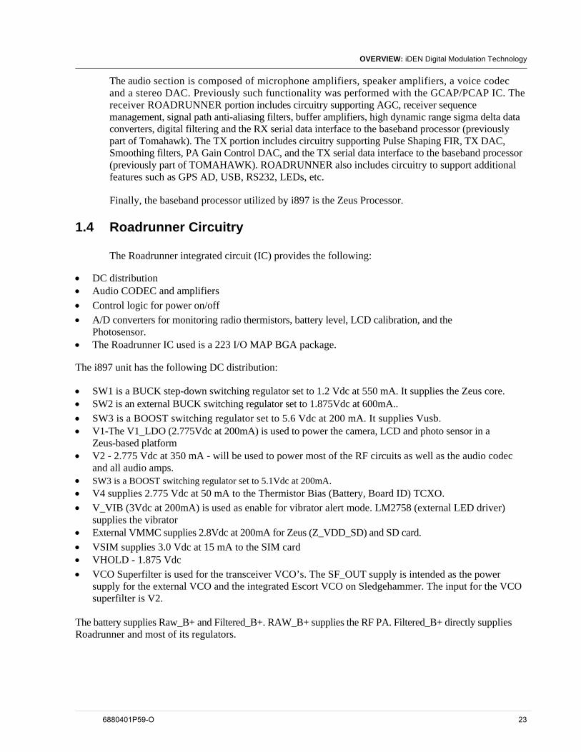
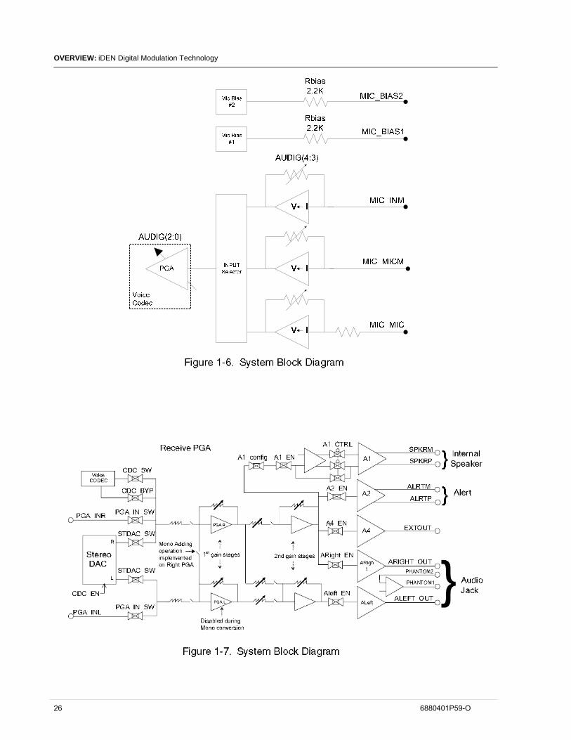
1.5.2 Audio Amplifiers The i897 uses seven audio amplifiers, five from the Roadrunner and 2 from an external class D amplifier, as shown and further described in the Figure 1-6, Figure 1-7 and Figure 1-1.
6880401P59-O 25
OVERVIEW: iDEN Digital Modulation Technology
26 6880401P59-O
OVERVIEW: iDEN Digital Modulation Technology
Table 1-1: Audio Amplifier Outputs and Acoustic Transducers
Outputs Acoustic Transducer
A1 (RR) Earpiece speaker output
A2 (RR) Unused
A3 (RR) Internal microphone input
A4 (RR) Audio jack output
A5 (RR) External microphone input
AL (Ext.) Left channel output to left channel high audio speaker (stereo) or earpiece speaker (mono)
AR (Ext.) Right channel output to left channel high audio speaker (stereo) or earpiece speaker (mono)
1.5.3 Audio Modes
The i897 audio circuitry has two basic modes of audio communication operation: interconnect and dispatch. It also has digital audio and digital video with digital audio multimedia playback modes.
In standard interconnect mode, the i897 uses Roadrunner's internal amplifiers to directly drive the dynamic earpiece speaker. It can also drive the two high audio speakers in mono if the speakerphone feature is enabled.
In standard dispatch mode, the i897 uses Roadrunner's internal amplifiers to directly drive the two high audio speakers in mono. It can also drive the dynamic earpiece speaker.
1.5.4 Audio Paths
The i897 can accept audio from the internal or external microphones. Interconnect voice, dispatch voice, dispatch tones, and ringer tones are also generated during audio communication operation. These received audio signals can be transmitted or routed to the earpiece speaker, high audio speakers, output depending on the audio mode of operation and state of the High/Low Speaker key and audio USB device detect circuit.
The High/Low Speaker key toggles the audio output from the high audio speakers to the earpiece speaker. The functionality of the High/Low Speaker key is disabled when there is an audio USB connect detected.
The microphone input can also be muted and unmuted at any time during an interconnect call.
6880401P59-O 27
OVERVIEW: Digital Section
1.5.5 Transmit Paths The average human voice signal has an audible frequency band of approximately 300 - 3400 Hz. Low pass filters are utilized to provide the optimum voice signal response on the mic signal line by filtering out unnecessary and potentially disruptive higher frequencies. The mic signal is then amplified by the Roadrunner's internal op-amp and then converted from analog to digital in the ADC. The digital mic signal is then digitally filtered, transferred to the DSP for necessary processing, and then sent to SLEDGEHAMMER. Lastly, the data is sent to JANUS and transmitted.
1.5.6 Receive Paths The received voice signal is first converted to digital by SLEDGEHAMMER and then sent to the DSP for necessary processing. The DSP sends the processed voice signal to the CODEC, where it is converted from digital to analog in its internal DAC. The output of the DAC is then band-pass filtered to attenuate any out-of-band noise.
Next, depending on the audio mode of operation and state of the High/Low Speaker key and audio jack detect circuit, the speaker signal is either sent to the Roadrunner amplifier to drive the earpiece speaker, the external 0.5W amplifier to drive the high audio speakers, or the audio jack output.
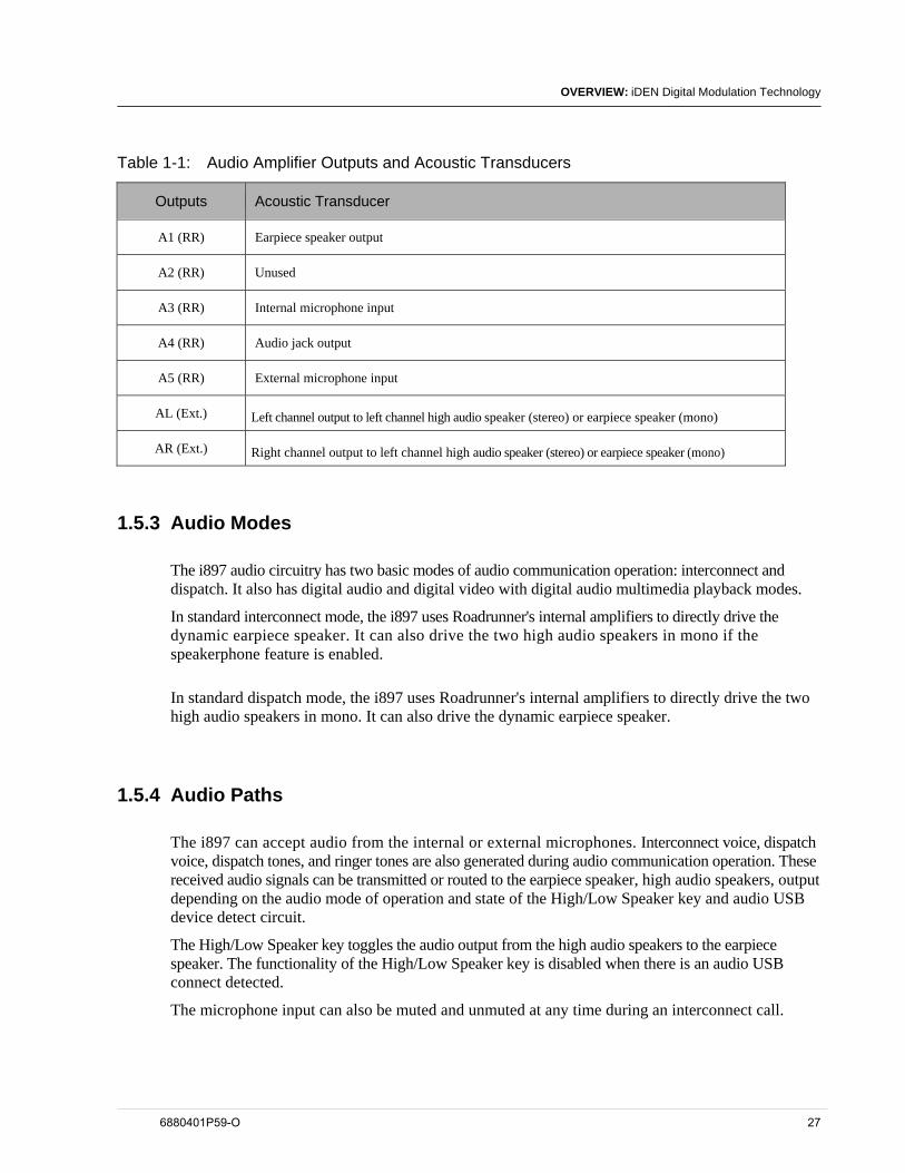
1.6 Digital Section
This section includes the Zeus which is a Dual Core Baseband Processor associated and external memories. The Zeus controls the transmit, receive, and synthesize operations of the integrated circuits located in the RF section.
The digital section contains the following (see Figure 1-8):
• Zeus Dual Core Baseband Processor • Host memories (NAND flash and DDR) • iDEN Power Management
Figure 1-8: iDEN Digital Block Diagram
28 6880401P59-O
OVERVIEW: Digital Section
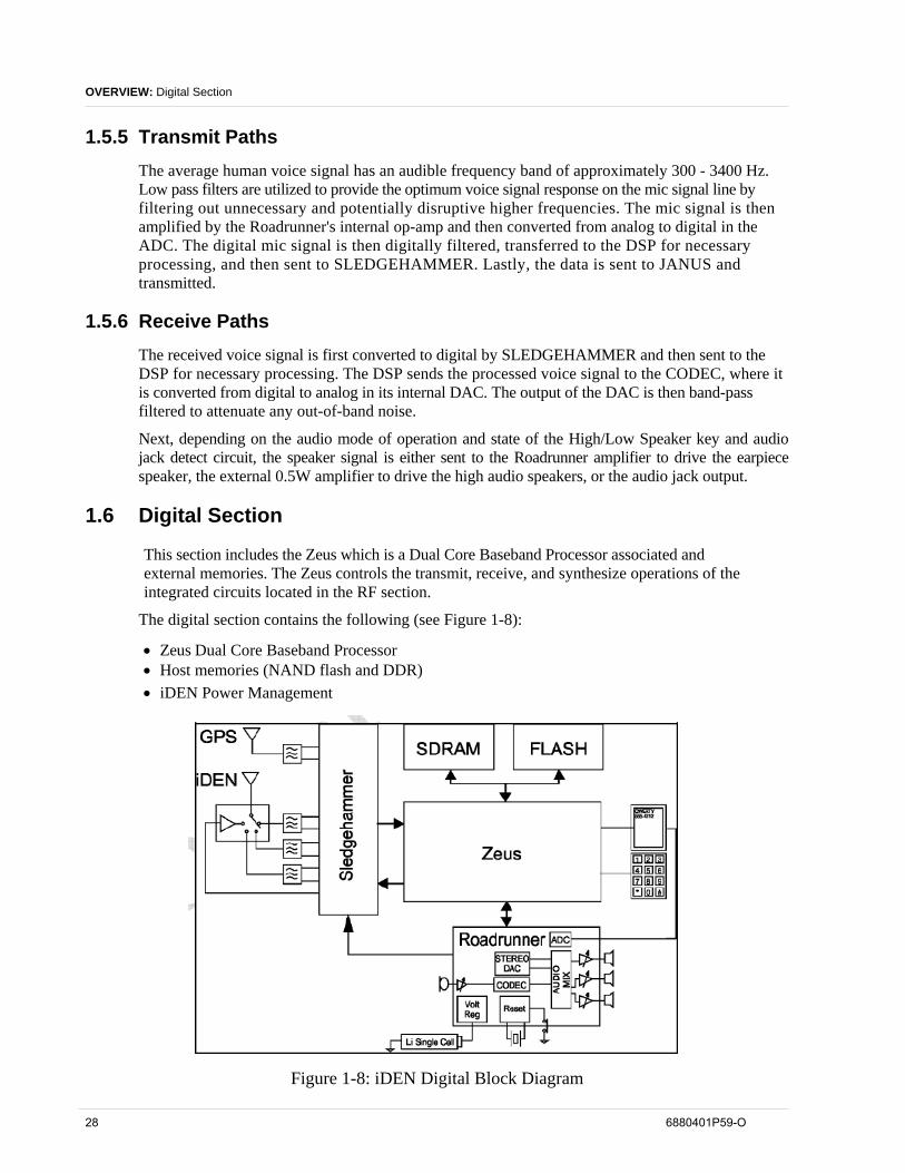
1.6.1 Zeus Processor
Zeus is a dual core (P2002 Starcore DSP and an ARM-11 Application Processor) processor with a shared memory system (see Figure 1-9).
The following is a summary of the ZEUS key features: The following is a list of ARM11 core features in the ARM1136JF-S AP subsystem: • Integer unit with integral Embedded ICE logic • Eight-stage pipeline • Branch prediction with return stack • Low-interrupt latency • Instruction and data Memory Management Units (MMUs), using MicroTLB structures backed by a
unified main TLB • Instruction and data L1 caches, including a non-blocking data cache with hit-under-miss • Virtually-indexed/physically-addressed L1 caches • 64-bit interface to both L1 caches • Write buffer (by-passable) • High-Speed Advanced Micro Bus Architecture (AM1BA) L2 interface • Vector Floating Point co-processor (VFP) hardware for acceleration of 3-D graphics and other
floating-point applications.
Figure 1-9. Zeus Functional Block Diagram 6880401P59-O 29
OVERVIEW: Digital Section
Zeus performs the following tasks: • Assists RoadRunner in the control of the power-up and power-down sequence of the unit. • USB communication with the factory Automated Test Equipment. • Accesses to the external NAND flash memory and DDR memory. • Communicates with the RF ICs (ROADRUNNER and SLEDGEHAMMER). • Memory mappings and accesses Liquid Crystal Display. • Monitors battery voltage, as well as RF power-amplifier and battery temperature. • Modifies and stores user-selectable ergonomic preferences. • Reads and writes iDEN radio-tuning parameters. • Sends and receives commands with the base station through DSP. • Re-channels the SLEDGEHAMMER synthesizer during hand off.
1.6.2 MCU Digital Phase Locked Loop (DPLL) The MCU has a programmable, digital phase locked loop (DPLL) that uses the 16.8 MHz clock as a reference. The MCU initially runs from the external reference at power up. Software programs the MCU DPLL to 399 MHz and switches from the external reference to the MCU DPLL after lock is reached
1.6.3 Host System Clock Synthesizer There are two iDEN system clocks that are generated by Roadrunner and Sledgehammer. The Roadrunner generates 32.768 kHz using the Roadrunner PLL, and the Sledgehammer generates 33.6 MHz. The MCU Programmable Interrupt Timer (PIT) is run by the 32.768 kHz oscillator. The 33.6 MHz is divided by 2 in the Roadrunner to yield a 16.8 MHz signal, which serves as reference frequency required by the MCU and DSP cores
1.6.4 Host System Clock Synthesizer The power-on circuitry uses the ROADRUNNER /ON B-pin and the power On/Off button to turn on the unit. When the On/Off button is pressed to turn on the unit, the ON pin is shorted to ground, which turns on ROADRUNNER. The low-voltage detector provides the initial, active low reset to the MCU. When the ROADRUNNER voltages become stable (after a minimum of 450 ms), the ROADRUNNER delays the voltage coming up, and supervisor IC that monitors the voltage on V2, recognizes this and holds off Reset. At this point, the MCU sets the defaults for all the ICs. For instance, the SLEDGEHAMMER default clock is set to 8.4 MHz (16.8 MHz divided by 2). The MCU must reprogram the SLEDGEHAMMER to run off the 16.8 MHz frequency. In addition, the ZEUS boots off of the High Clock, not the Low Clock (CKIL). At this point, the ZEUS begins running the subscriber code. To turn off the unit, the On/Off button is pressed, causing the /ON B-pin of the ROADRUNNER to short to ground. The ROADRUNNER which drives ROADRUNNER SEL_INT on ZEUS and tells the MCU to turn off. The MCU turns off by driving the STO (WDI input to ROADRUNNER) line low, which shuts down the voltage regulators in the ROADRUNNER.
30 6880401P59-O
OVERVIEW: Digital Section
1.6.5 ZEUS Digital Signal Processor
The Zeus digital signal processor contains the DSP Engine SC140e:
The following is a list of SC140e features that make this core ideal for a single core modem: • StarCore™ SC1000 architecture foundation • 16-Kbyte instructions and 32-Kbyte Data Level 1 caches • Supervisor- and user-mode task protection • Memory Management Unit (MMU) tailored to real-time applications • Compiled C code density on par with the MCU’s • Branch penalty-minimization with a short, five-stage pipeline • Low interrupt latency • Four arithmetic-logic unit (ALU) architecture • 4-Gbyte linear address range support.
1.6.6 DSP Phase Locked Loop (PLL) The DSP PLL is programmable and is used to generate a DSP internal clock that is synchronized to the 16.8 MHz reference frequency. In low power mode, the DSP PLL is disabled and the DSP operates directly from the 16.8 MHz clock. The DSP PLL runs at 208 MHz.
1.6.7 Serial Peripheral Interface (SPI) This interface communicates with RF chips using the SPI bus. This bus includes the following: • Master Out Slave In (MOSI) • Master In Slave Out (MISO) • SPI clock • Specific chip-select lines
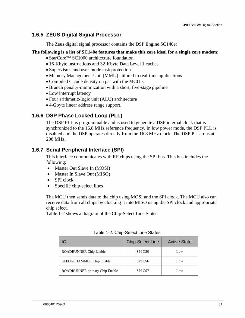
The MCU then sends data to the chip using MOSI and the SPI clock. The MCU also can receive data from all chips by clocking it into MISO using the SPI clock and appropriate chip select. Table 1-2 shows a diagram of the Chip-Select Line States.
Table 1-2. Chip-Select Line States
IC Chip-Select Line Active State
ROADRUNNER Chip Enable SPI CS0 Low
SLEDGEHAMMER Chip Enable SPI CS6 Low
ROADRUNNER primary Chip Enable SPI CS7 Low
6880401P59-O 31
OVERVIEW: Digital Section
1.6.8 System Memory The following types of memories are used in i897:
1. 256MB (2Gbit) of NAND flash memory used to store unit subscriber and DSP code. 2. 128MB (1Gbit) of DDR memory used by the MCU to load code-plug information,
program the flash, and store working parameters. The DDR operates at 266MHz. Both memories are external to the processor and are stacked in the same package.
1.6.9 USB2.0 I897 supports USB2.0 High Speed rate of 480Mbps. The file transfer throughout rate is
about 2MB/s for high speed transfers. The phone also supports USB1.1 Full Speed host. Basically there are two USB paths in the design, high speed and full speed. Whenever a
USB data cable is connected to the phone, it defaults to High Speed mode. In this mode, the USB interface goes through a USB2.0 Controller IC (CY7C68053-56BAXI from Cypress). Only for flashing/programming and RS232 (Y-cable berbug) communication, the USB interface goes through the existing Full Speed EMU IC. There is a switch on board, controlled by Zeus, to switch between these 2 paths. For the
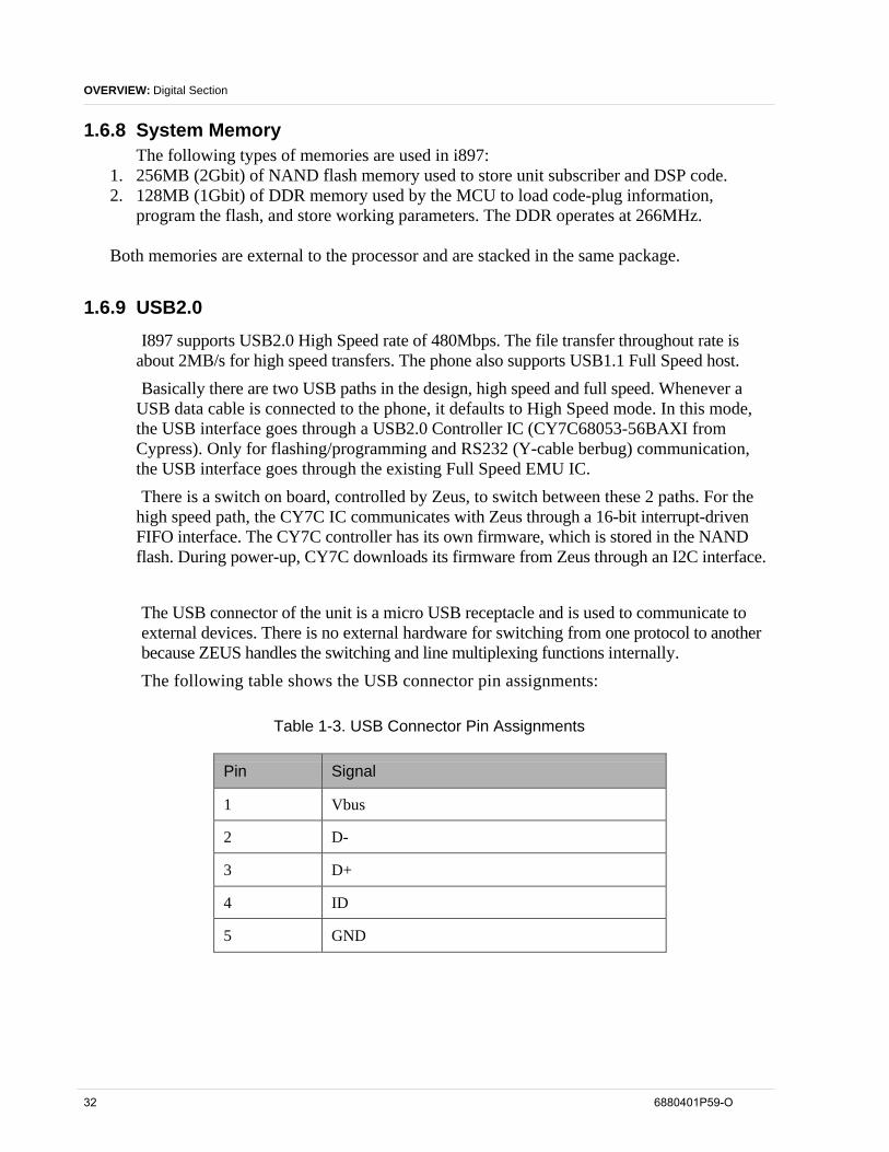
high speed path, the CY7C IC communicates with Zeus through a 16-bit interrupt-driven FIFO interface. The CY7C controller has its own firmware, which is stored in the NAND flash. During power-up, CY7C downloads its firmware from Zeus through an I2C interface. The USB connector of the unit is a micro USB receptacle and is used to communicate to external devices. There is no external hardware for switching from one protocol to another because ZEUS handles the switching and line multiplexing functions internally. The following table shows the USB connector pin assignments:
Table 1-3. USB Connector Pin Assignments
Pin Signal
1 Vbus
2 D-
3
D+
4 ID
5 GND
32 6880401P59-O
OVERVIEW: Digital Section
1.6.10 Battery ID The battery is equipped with a Dallas 2502 EPROM. A two-wire serial bus allows the i897 unit or the battery charger to communicate with the battery and identify whether or not the battery is compatible. If the battery is determined to be incompatible, the charger does not enter charging mode.
Besides compatibility data, the EPROM also stores such information as the battery type, capacity, fuel-gauging parameters, and voltage thresholds.
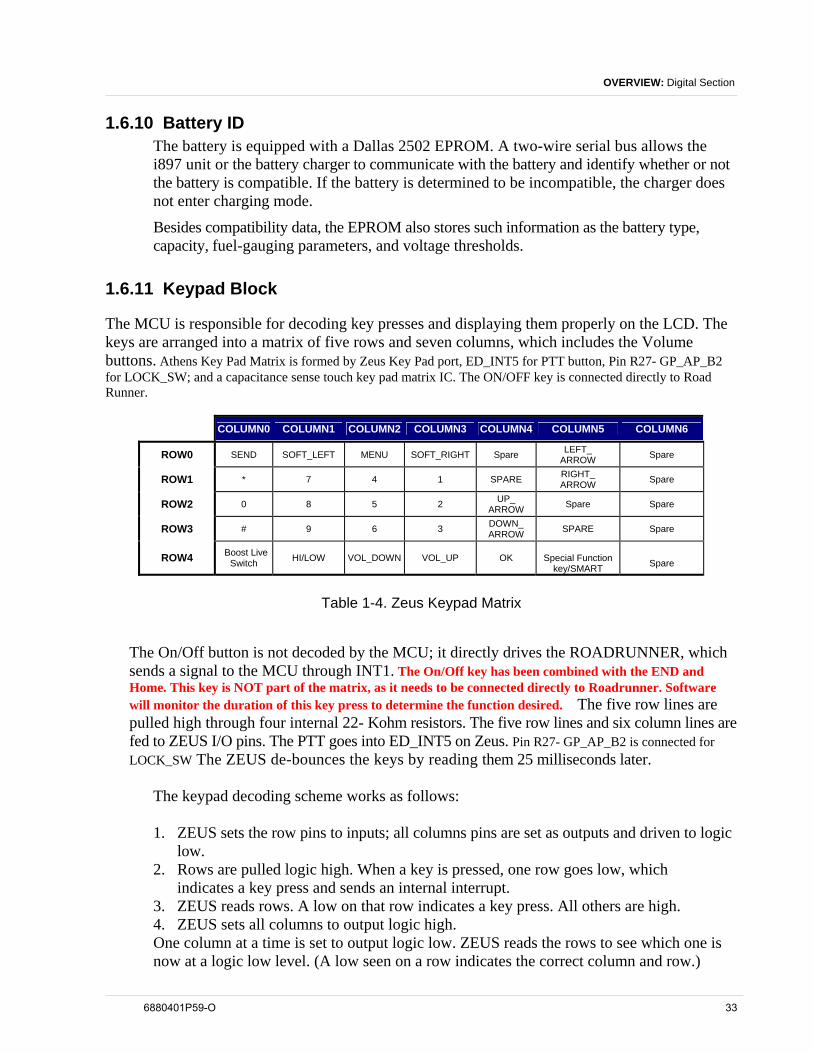
1.6.11 Keypad Block
The MCU is responsible for decoding key presses and displaying them properly on the LCD. The keys are arranged into a matrix of five rows and seven columns, which includes the Volume buttons. Athens Key Pad Matrix is formed by Zeus Key Pad port, ED_INT5 for PTT button, Pin R27- GP_AP_B2 for LOCK_SW; and a capacitance sense touch key pad matrix IC. The ON/OFF key is connected directly to Road Runner.
COLUMN0 COLUMN3 COLUMN4COLUMN1 COLUMN2 COLUMN5 COLUMN6
ROW0 SEND SOFT_LEFT MENU SOFT_RIGHT Spare LEFT_ ARROW Spare
ROW1 * 7 4 1 SPARE RIGHT_ Spare ARROW
ROW2 0 8 5 2 UP_ Spare Spare ARROW
ROW3 # 9 6 3 DOWN_ SPARE Spare ARROW Boost Live
Switch ROW4 HI/LOW VOL_DOWN VOL_UP OK Special Function key/SMART Spare
Table 1-4. Zeus Keypad Matrix
The On/Off button is not decoded by the MCU; it directly drives the ROADRUNNER, which sends a signal to the MCU through INT1. The On/Off key has been combined with the END and Home. This key is NOT part of the matrix, as it needs to be connected directly to Roadrunner. Software will monitor the duration of this key press to determine the function desired. The five row lines are pulled high through four internal 22- Kohm resistors. The five row lines and six column lines are fed to ZEUS I/O pins. The PTT goes into ED_INT5 on Zeus. Pin R27- GP_AP_B2 is connected for LOCK_SW The ZEUS de-bounces the keys by reading them 25 milliseconds later.
The keypad decoding scheme works as follows: 1. ZEUS sets the row pins to inputs; all columns pins are set as outputs and driven to logic
low. 2. Rows are pulled logic high. When a key is pressed, one row goes low, which
indicates a key press and sends an internal interrupt. 3. ZEUS reads rows. A low on that row indicates a key press. All others are high. 4. ZEUS sets all columns to output logic high. One column at a time is set to output logic low. ZEUS reads the rows to see which one is now at a logic low level. (A low seen on a row indicates the correct column and row.)
6880401P59-O 33
OVERVIEW: Digital Section
1.6.12 LCD Circuit The LCD circuit consists of a full-graphics, liquid-crystal display module that has a resolution of 240RGBx320pixels, 262K colors. The data lines for the display module are connected to RGB 6:6:6 (18 bits) and control interface from the IPU section of the Zeus processor. The display module booster voltage is powered by V1 (2.775 V), the I/O is powered by SW2 (1 .875 V). The display module connects to the flip PCB through a 54-pin connector and the flip PCB connects to keypad flex through a 60-pin connector. Then to the keypad flex through a 80-pin connector which in turn connects to the main.
1.6.13 CMOS 2.0 Mega-pixel Focus Camera The camera is a 2-Megapixel, color CMOS image sensor with Bayer (Green, Red, Green, and Blue) patter filter and no auto focus features. This device provides a finished image at up to 15fps (frames per second) image data at 1200 X 1600 resolutions and up to 320 x 240 resolutions to enable video clip capture. It resides on the camera flex circuit connecting to Flippcb through the 30-pin connector.
Control of the camera settings from Zeus is via I2C serial interface, using 8bits data transfers.
34 6880401P59-O
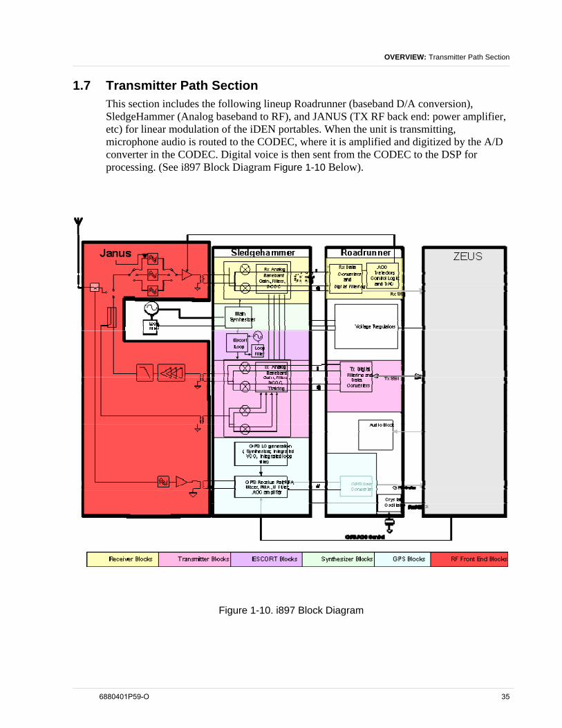
OVERVIEW: Transmitter Path Section
1.7 Transmitter Path Section This section includes the following lineup Roadrunner (baseband D/A conversion), SledgeHammer (Analog baseband to RF), and JANUS (TX RF back end: power amplifier, etc) for linear modulation of the iDEN portables. When the unit is transmitting, microphone audio is routed to the CODEC, where it is amplified and digitized by the A/D converter in the CODEC. Digital voice is then sent from the CODEC to the DSP for processing. (See i897 Block Diagram Figure 1-10 Below).
Figure 1-10. i897 Block Diagram
6880401P59-O 35
OVERVIEW: Transmitter Path Section
The JANUS transmitter module includes the following:
• Center tapped RF balun for RFPA differential input
• High Power Linear RFPA
• RFPA Load line switch selection mode.
• Reduced quiescent current selection mode.
• Directional coupler.
• Low pass harmonic filter.
The DSP performs VSELP data compression and generates digital I & Q words to be transmitted to the ROADRUNNER. The signal then is sent at a rate of 48 K samples per second. The ROADRUNNER provides the serial clock to the DSP and a frame sync pulse to tell the DSP to send a sample. Each sample is sent as a 16-bit I word followed by a 16-bit Q word and then some meaningless fill bits.
The I word and the Q word are then converted to an analog differential pair by the ROADRUNNER and amplified. The ROADRUNNER also sends a 4.2 MHz reference clock signal to the SLEDGEHAMMER, together when a DMCS and TXE signal are received from the DSP. The TXE transition starts the TX sequence with SLEDGEHAMMER, which entails the training sequences as well as enabling the antenna switch and PA.
DMCS signals the start of data being sent from DSP to ROADRUNNER. Once the transmit burst is finalized, the TX shutdown is done by disabling TXE and DMCS.
1.7.1 ROADRUNNER The ROADRUNNER IC is designed as a derivative of several other ICs previously used in iDEN products. The ROADRUNNER IC includes the following blocks:
RX:
• ADC • Digital Filtering
TX:
• Digital interface (the transmitter receives inputs from the SSI. The SSI has a single data line).
• Pulse Shaping FIR (A programmable waveform generator "FIR" filter provides interpolation of the pre shaped input words).
• TX DAC (The transmit DACs have eleven bit resolution and are capable of supporting 8.4 Mbits). Fine step TX attenuation (cutback).
Smoothing filters (programmable RC smoothing filters limit the amount of far out quantization noise and images due to aliasing. The filters incorporate a dc offset correction block).
36 6880401P59-O
OVERVIEW: Transmitter Path Section
ROADRUNNER Transmit Operation. The transmitter implemented a Direct Conversion Transmitter (DCT), where base band data is up-converted into RF with only one stage. The ICs that perform the transmit operations are ROADRUNNER and SLEDGEHAMMER. Power cutback control is shared between both ICs, the fine cutback step (1-> 4dB) is performed by ROADRUNNER and the coarse cutback step (5 dB steps up to 35 dB) is performed by SLEDGEHAMMER. To generate the RF signal, the SLEDGEHAMMER IC uses a TX_LO that is centered at the carrier frequency. This TX_LO is generated INSIDE SLEDGEHAMMER.
The digital samples are generated by the DSP and then sent to ROADRUNNER via Transmit SSI (TX_S SI). ROADRUNNER then implements the Digital-to-Analog Conversion function, which provides some power control function. The resulting I!Q analog signals are then sent to the SLEDGEHAMMER IC, which up-converts the base band signal to RF (similar to what the JAVELIN did on previous architectures).
The I!Q path circuits will be similar to the lineup used in the Tomahawk IC. The "main" reconstruction filter for the I!Q paths will be located in the SLEDGEHAMMER IC, and will have programmable BW options of 25, 50, and 100 KHz.
These functions of the IQ modulator consist of the interface to the digital baseband, the digital baseband sub-block, the analog baseband sub-block, and the TX DAC bridging the digital and analog sub-blocks. The ROADRUNNER IC will produce the baseband I and Q signals needed for IQ modulation on the SLEDGEHAMMER IC.
1.7.2 Sledgehammer IC (TX Path) The SLEDGEHAMMER is the heart of the transmitter; it incorporates all of the circuitry necessary to implement a Cartesian feedback closed-loop system.
The differential baseband signals from the ROADRUNNER are input into the SLEDGEHAMMER. They go through a variable attenuator and are then summed with the down-converted I & Q feedback. The baseband signal is then amplified and sent to the up mixers.
1.7.3 JANUS JANUS is a RF front end module (FEM) intended to support iDEN and WiDEN protocols.
The JANUS FEM contains the RF front end functions for the iDEN receiver, iDEN transmitter and GPS receiver. The JANUS FEM is intended to be used as part of the iDEN Phoenix Platform, and it is also backwards compatible with the existing Falcon platform.
The transmitter section of Janus comprises a single lineup that support iDEN 800MHz, iDEN 900MHz and Mototalk. The TX balun presents a differential impedance to the modulator on the RFIC, and it also feeds RAW _B+ to the modulator via the TX_IN and TX_INB pins. The nominal differential impedance to the TX balun is 200ohms.
The RFPA also features a 2.5dB load line select line as well as reduced quiescent current mode for low output power operation.
6880401P59-O 37
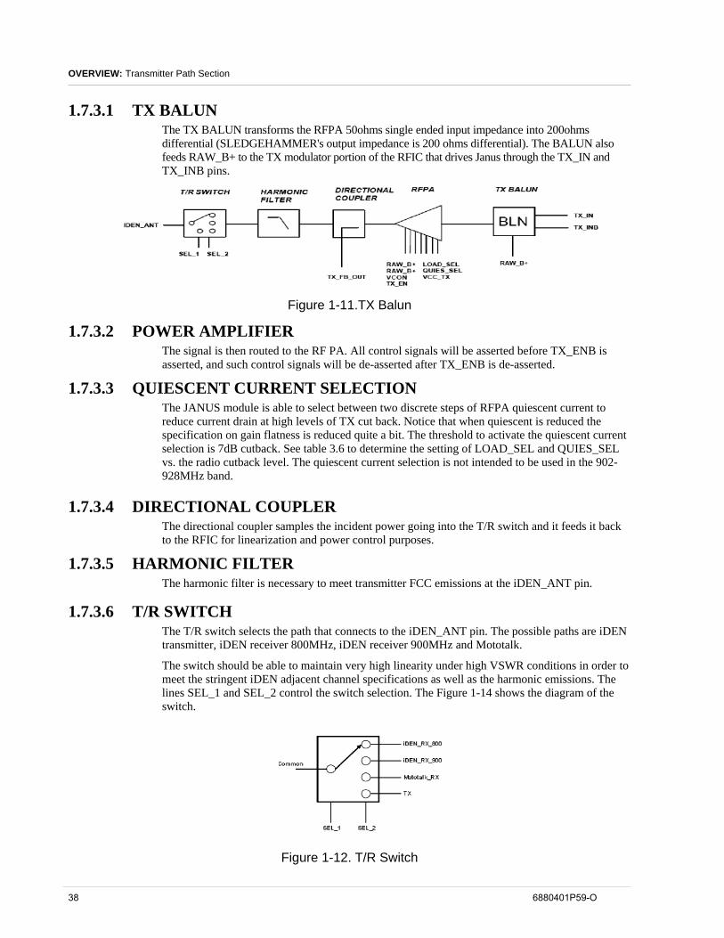
OVERVIEW: Transmitter Path Section
1.7.3.1 TX BALUN The TX BALUN transforms the RFPA 50ohms single ended input impedance into 200ohms differential (SLEDGEHAMMER's output impedance is 200 ohms differential). The BALUN also feeds RAW_B+ to the TX modulator portion of the RFIC that drives Janus through the TX_IN and TX_INB pins.
Figure 1-11.TX Balun
1.7.3.2 POWER AMPLIFIER The signal is then routed to the RF PA. All control signals will be asserted before TX_ENB is asserted, and such control signals will be de-asserted after TX_ENB is de-asserted.
1.7.3.3 QUIESCENT CURRENT SELECTION The JANUS module is able to select between two discrete steps of RFPA quiescent current to reduce current drain at high levels of TX cut back. Notice that when quiescent is reduced the specification on gain flatness is reduced quite a bit. The threshold to activate the quiescent current selection is 7dB cutback. See table 3.6 to determine the setting of LOAD_SEL and QUIES_SEL vs. the radio cutback level. The quiescent current selection is not intended to be used in the 902- 928MHz band.
1.7.3.4 DIRECTIONAL COUPLER The directional coupler samples the incident power going into the T/R switch and it feeds it back to the RFIC for linearization and power control purposes.
1.7.3.5 HARMONIC FILTER The harmonic filter is necessary to meet transmitter FCC emissions at the iDEN_ANT pin.
1.7.3.6 T/R SWITCH The T/R switch selects the path that connects to the iDEN_ANT pin. The possible paths are iDEN transmitter, iDEN receiver 800MHz, iDEN receiver 900MHz and Mototalk.
The switch should be able to maintain very high linearity under high VSWR conditions in order to meet the stringent iDEN adjacent channel specifications as well as the harmonic emissions. The lines SEL_1 and SEL_2 control the switch selection. The Figure 1-14 shows the diagram of the switch.
Figure 1-12. T/R Switch
38 6880401P59-O
OVERVIEW: Transmitter Path Section
1.7.3.7 TEMPERATURE SENSOR A temperature sensor is included in the Janus module. The sensor is located close to the SAW filter whose temperature raises the most during TX operation.
The preferred implementation for the sensor is a thermistor Panasonic ERTJZEP473J connected between GND and PA_TEMP.
1.7.4 Cartesian Feedback The iDEN transmitters use MQAM modulation, which requires a highly linear PA with wide dynamic range. Linear PAs are highly inefficient, so a class AB PA is used for better efficiency and longer battery life. The class AB PA is fairly linear, but not totally, and this causes splatter in the RF spectrum around the transmitted frequency band. To reduce splattering into the adjacent channels and to meet system specifications, the transmitter uses Cartesian feedback to linearize the PA and reduce splatter. Negative feedback is a commonly used method to linearize circuits.
Cartesian feedback is the process of down converting the feedback signal to baseband and summing it with the input signal in the I & Q paths separately. One can control the 180º phase shift at baseband more precisely than at RF frequencies. The SLEDGEHAMMER is the heart of the Cartesian feedback system, and as such, is the heart of the transmitter. There is a forward path and a feedback path in the transmitter. This is a closed loop system and the loop cannot be opened without drastic consequences. (See i897 Block Diagram Figure 1-13 Below). (TX interface between SLEDGEHAMMER and JANUS).
Figure 1-13. i897 Block Diagram
6880401P59-O 39
OVERVIEW: Transmitter Path Section
The forward path includes the following:
• SLEDGEHAMMER • JANUS (Balun, Power amplifier, Coupler)
The feedback path includes the following:
• Coupler • Feedback attenuation network. • SLEDGEHAMMER
1.7.5 Level Set and Phase Training Level set training is performed to ensure that the RF PA is not driven into clip, which would result in excess splatter and out-of-band spurious emissions. During training, the DSP signal is disconnected from the forward path and an internal analog ramp generator is connected. The feedback is monitored and compared to the analog ramp. As the ramp amplitude increases and the RF PA begins to clip, the error voltage increases. See Figure 1-16 on page 33.
The Javelin levelset circuit topology is modified slightly for Sledgehammer. The major difference is that switches are not provided to select the I-channel training waveform to the Q-channel V-I input. Instead, a programmable gain V-I is specified below on the Ichannel for boosting the reference signal level during level training. The "cnrmp" control signal is output from the levelset circuit to the I-channel V-I to control when the gain is changed.
V_TERM is a new signal input that will be OR'ed with the clip comparator output. This signal causes a controlled signal ramp down when the battery current exceeds 3A during level training. V_TERM OR'ed with the clip comparator output is sent back to the digital core to terminate the counter used for the LEVEL _TRAIN read back value
40 6880401P59-O
OVERVIEW: Transmitter Path Section
Negative feedback is required to maintain system stability. Phase training is done to ensure that the feedback is negative (180º). The phase shift of the loop consists of the sum of the delays of several modules and components.
Operation of the Sledgehammer in a closed loop system requires the phase of the feedback path to be adjusted with respect to the forward path such that the demodulated feedback signal is the correct phase at the summing junction. This adjustment needs to take place before the loop is closed and data is transmitted, and is referred to as the 'phase training period'.
The maximum peak input signal to Sledgehammer is also scaled via the Roadrunner/DSP to insure that the maximum input signal in the data will not cause clipping to occur in the power amplifier output as a result of temperature/voltage gain variation in the forward path (primarily the power amplifier). The scaling of the input signal is a result of 'level training' which is performed in the transmit slot prior to data transmission. When level set training was implemented on the Tranlin and ODCT IC, training was done autonomously on the IC. Most of the level set circuitry was removed on the JANUS for cost savings. SLEDGEHAMMER training methods will be based on the JANUS design. The scaling of the input signal and the ramping is now performed by the DSP.The ramp signal will be applied from the DSP, and will go through the signal path of the Roadrunner IC with the gain set to maximum. The loop will be closed, but the slew rate limiter will be in a low gain (low slew) mode. A counter on the Sledgehammer will begin counting from the beginning of the timing event associated signal 'LAGC' and its' associated timing parameter "D". The loop will perform an AGC function in the beginning portion of the ramp in order to set the loop gain and then hold this gain value.
When the clip detect comparator determines that the loop can no longer compensate for the PA, it will disconnect the Roadrunner input and allow the slew rate limiter to ramp the signal down in a controlled manner to prevent splatter. After clip has been detected, and before the beginning of data, a SPI read is necessary for the DSP to find out at what point in time the clip occurred. Based on this information, a reference level will be set in the Roadrunner. Providing level set in this manner will require at least two SPI activities. The first activity is to read back the timing value "D" from the Sledgehammer IC. The second is to write the gain setting for the Roadrunner.
Both phase and level training are required at least once before transmission of the data in the first slot, but not necessarily performed in every transmit slot. DC training will be performed at the start of every SLOT. All timer values associated with SLOT rising edge will be increased with respect to JANUS program values to account for the DC training time.
Unlike JANUS, Sledgehammer provides the ability to terminate the level training ramp by either the internal Sledgehammer clip detector or an external control digital signal V_TERM. V_TERM indicates when the battery current exceeds 3 Amps, which is used to terminate the training ramp to avoid an early radio shutdown during level training.
Shutdown is avoided by lowering the transmit power when V_TERM is detected. This signal goes directly to the levelset circuitry.
6880401P59-O 41
OVERVIEW: Receiver Path Section
1.8 Receiver Path Section The receiver is a direct conversion receiver. It operates in the commercial portion of the land-mobile receiver band (851-870MHz and 935-940). The receiver takes an incoming RF signal, down-converts it to baseband where it is then amplified, filtered, digitized and then provided to the DSP MODEM. The receiver has, automatic gain control (AGC) to maintain good linearity over a wide range of incoming signals.
The receiver has automatic gain control (AGC) to maintain good linearity over a wide range of incoming signals. The AGC circuitry also prevents clipping of high-level signals.
Janus block, which is a receiver circuitry path for TAOS (See i897 Block Diagram Figure 1-14 Below).
Figure 1-14. i897 Block Diagram
42 6880401P59-O
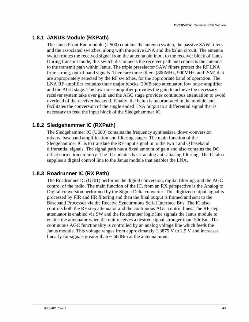
OVERVIEW: Receiver Path Section
1.8.1 JANUS Module (RXPath) The Janus Front End module (U500) contains the antenna switch, the passive SAW filters and the associated switches, along with the active LNA and the balun circuit. The antenna switch routes the received signal from the antenna pin input to the receiver block of Janus. During transmit mode, this switch disconnects the receiver path and connects the antenna to the transmit path within Janus. The triple preselector SAW filters protect the RF LNA from strong, out-of band signals. There are three filters (800MHz, 900MHz, and ISM) that are appropriately selected by the RF switches, for the appropriate band of operation. The LNA RF amplifier contains three major blocks: 20dB step attenuator, low noise amplifier and the AGC stage. The low-noise amplifier provides the gain to achieve the necessary receiver system take over gain and the AGC stage provides continuous attenuation to avoid overload of the receiver backend. Finally, the balun is incorporated in the module and facilitates the conversion of the single ended LNA output to a differential signal that is necessary to feed the input block of the Sledgehammer IC.
1.8.2 Sledgehammer IC (RXPath) The Sledgehammer IC (U600) contains the frequency synthesizer, down-conversion mixers, baseband amplification and filtering stages. The main function of the Sledgehammer IC is to translate the RF input signal in to the two I and Q baseband differential signals. The signal path has a fixed amount of gain and also contains the DC offset correction circuitry. The IC contains basic analog anti-aliasing filtering. The IC also supplies a digital control line to the Janus module that enables the LNA.
1.8.3 Roadrunner IC (RX Path) The Roadrunner IC (U701) performs the digital conversion, digital filtering, and the AGC control of the radio. The main function of the IC, from an RX perspective is the Analog to Digital conversion performed by the Sigma Delta converter. This digitized output signal is processed by FIR and IIR filtering and then the final output is framed and sent to the Baseband Processor via the Receive Synchronous Serial Interface Bus. The IC also controls both the RF step attenuator and the continuous AGC control lines. The RF step attenuator is enabled via SW and the Roadrunner logic line signals the Janus module to enable the attenuator when the unit receives a desired signal stronger than -50dBm. The continuous AGC functionality is controlled by an analog voltage line which feeds the Janus module. This voltage ranges from approximately 1.3875 V to 2.5 V and increases linearly for signals greater than ~-60dBm at the antenna input.
6880401P59-O 43
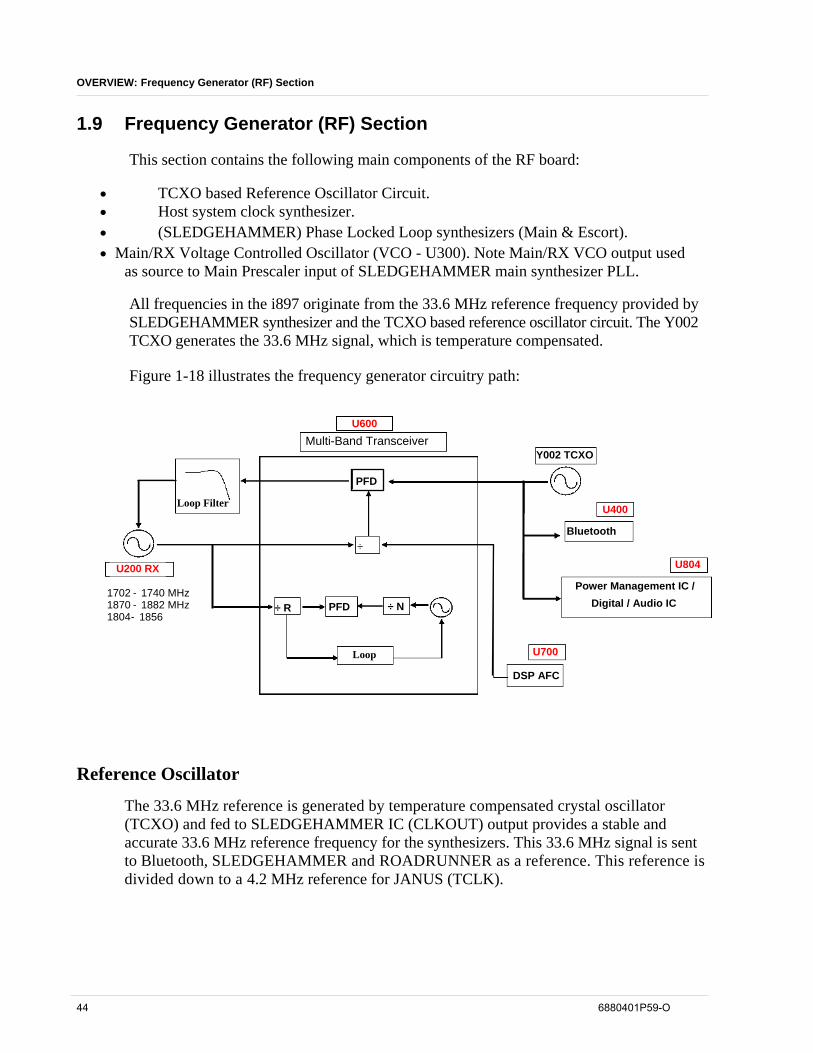
OVERVIEW: Frequency Generator (RF) Section
1.9 Frequency Generator (RF) Section
This section contains the following main components of the RF board:
• TCXO based Reference Oscillator Circuit. • Host system clock synthesizer. • (SLEDGEHAMMER) Phase Locked Loop synthesizers (Main & Escort). • Main/RX Voltage Controlled Oscillator (VCO - U300). Note Main/RX VCO output used
as source to Main Prescaler input of SLEDGEHAMMER main synthesizer PLL.
All frequencies in the i897 originate from the 33.6 MHz reference frequency provided by SLEDGEHAMMER synthesizer and the TCXO based reference oscillator circuit. The Y002 TCXO generates the 33.6 MHz signal, which is temperature compensated.
Figure 1-18 illustrates the frequency generator circuitry path:
U300
U600
Multi-Band Transceiver Y002 TCXO
Bluetooth
Power Management IC /Digital / Audio IC
DSP AFC
1702 - 1740 MHz 1870 - 1882 MHz 1804 - 1856
Loop Filter
÷ R PFD
Loop
÷
÷ N
PFD
U400
U804
U700
U200 RX
Reference Oscillator
The 33.6 MHz reference is generated by temperature compensated crystal oscillator (TCXO) and fed to SLEDGEHAMMER IC (CLKOUT) output provides a stable and accurate 33.6 MHz reference frequency for the synthesizers. This 33.6 MHz signal is sent to Bluetooth, SLEDGEHAMMER and ROADRUNNER as a reference. This reference is divided down to a 4.2 MHz reference for JANUS (TCLK).
44 6880401P59-O
OVERVIEW: Global Positioning System (GPS) Section
1.10 Global Positioning System (GPS) Section
The U.S. Department of Defense (DoD) operates a constellation of 24-satellites, employed for location and/or navigational purposes, on earth. These satellite vehicles (SV) operate in circular orbits, round the earth every 12 hours, at an altitude of 20,200 km. The SVs transmit earth-bound radio signals at a 1575.42 MHz fixed carrier frequency—an L1 band for non-military applications. Since the SVs utilize one carrier frequency, by employing a Spread Spectrum modulation technique, each SV can be uniquely identified from an assigned Pseudo-random Noise (PN) Code.
To determine a location on earth, a receiver must be built that can receive the simultaneous signals from the satellites that are in view of the receiver and use that information to calculate the location of the receiver. The receiver must pick up the signals from 4 satellites. Once the 4 satellites are located, the receiver measures the time it took for the satellite signals to arrive. From this timing information, the distance between the receiver and each satellite can be calculated. The four satellites’ ephemeris data provide the satellite’s X, Y, and Z positions. The range, R, is the receiver measurement made by calculating the time it took for the signal to reach the receiver. The user’s position, (Ux, Uy, Uz), and the clock bias, Cb, is then calculated.
To use the GPS, a receiver that can receive the spread-spectrum signals must be built. The detected signals are then converted from RF signals into appropriate digital input formats. These digital inputs are processed and converted into position information.
1.10.1 GPS Receiver A block diagram of the receiver for the i897 is shown in Figure 1-19. The GPS receiver is based on the SiRF SiRFStarIII GPS chipset.
6880401P59-O 45
OVERVIEW: Global Positioning System (GPS) Section
1.10.2 GPS Antenna The GPS antenna is common part of the tri-band antenna common to the iDEN antenna
1.10.3 JANUS IC The JANUS IC is a multi-purpose IC that host 4 critical parts of the GPS line up.
1.10.3.1 DIPLEXER This diplexer is used to isolate the GPS signal from the iDEN signal.
1.10.3.2 HIGH PASS FILTER The high pass filter provides further isolation from the iDEN signal.
1.10.3.3 GPS LNA GPS LNA is the front end GPS LNA. Expect about 18 dB of gain through this LNA.
1.10.3.4 SAW FILTER This SAW filter is to enhance the iDEN to GPS isolation and it works as a Balun that converts the signal ended signal to a differential signal.
1.10.4 GPS Receiver SLEDGEHAMMER IC is a multi-purpose IC that hosts a number of components in the GPS lineup. For GPS, the SLEDGEHAMMER IC mainly mixes down the differential RF signal to differential IF signal and provides the GPS clock to the next stage
1.10.5 GPS Receiver The ROADRUNNER IC is mainly a DC management IC but also converts the analog GPS IF signal to digital signal ready to be processed by the ZEUS IC.
1.10.6 GPS Receiver
The ZEUS IC is the main processor for the radio. The ZEUS IC also processes the GPS signal to calculate the GPS locations and provides the GPS AGC control to the SH IC.
1.10.7 GPS Receiver
A 33.6 MHz clock signal is used by the SH rf circuit as the frequency reference for its internal local oscillator. This clock is a temperature compensated crystal oscillator whose frequency accuracy is held to within 0.5 ppm. The high accuracy of the clock frequency plays a critical role in determining the time it takes to calculate the position coordinates.
1.10.8 GPS Receiver The baseband digital signals are input to the SiRF processor circuit (integrated in ZEUS) which in turn computes the position information. Once the position is determined, it is communicated to the handset microprocessor and displayed on the screen for personal use or transmitted to the base station for E911 as required
46 6880401P59-O
OVERVIEW: Bluetooth® Wireless System
1.11 Bluetooth® Wireless System Bluetooth technology is used for short range wireless communications that do not require high data rates. The original usage models included telephone, headsets, low-data rate access point, file transfer, and automatic synchronization. The newer usage models have added human interface devices, remote control, print capability, cable replacements and personal area networks.
Bluetooth devices use GFSK modulation in the 2.4 to 2.4835 GHz band. The channels have a bandwidth of 1 MHz. Frequency hopping is used to provide immunity to interference. The master unit in a pico-net dictates the hopping sequence at a rate of 1600 hops per second. This translates to a 625 uS transmission. The maximum data rate through a Bluetooth device is 3 Mb per second.
6880401P59-O 47

This Page Left Blank Intentionally
48 6880401P59-O
PREPARING FOR FIELD LEVEL TESTING: Preparing Equipment for Testing
Chapter 2
PREPARING FOR FIELD LEVEL TESTING Field level testing requires external equipment and support. To conduct field level trouble-shooting and testing of an i897 unit, you must become familiar with the screen readouts of the recommended test equipment.
Display screens provide information that is useful for troubleshooting purposes. Refer to Chapter 3 for information on the displays, errors, alert tones, and messages associated with this unit.
2.1 Preparing Equipment for Testing To ensure accurate testing of an i897 unit, it is important that the test equipment function properly.
2.1.1 Calibrating Equipment Test equipment should be internally calibrated before being used for testing. Note that the internal calibration does not substitute for a factory calibration. For more information, refer to R-2660 Digital Communications System Analyzer Operator’s Manual.
2.1.2 Checking the RF Cable Check the cable connection and quality to ensure that the test results are true. Cable length is criti cal to consistent Rx sensitivity and Tx power measurements. Use a high-quality, shielded, 50-ohm, coaxial cable that is approximately 1.5 feet in length. Place the unit to be tested at least 6 inches from the call box. The cable loss should be less than 2 dB.
2.1.3 Strong-Signal Environments
When using the R-2660 Communications System Analyzer to test a unit in a strong-signal environment (–75 dBm or stronger), change the bandmap of the unit.
For Registration/Call testing: Power up the unit. Immediately after hearing the beep, press Start on the R-2660. The unit will lock onto the first strong signal.
2.1.4 Protecting Static-Sensitive Devices
This unit contains static-sensitive devices that must be protected when opening the unit, or storing and transporting any printed-circuit board. Consider the following information to create a proper ground:
• Ground the working surface of your service bench. If possible, use the Motorola Static Protection Assembly (P/N 01803 86A82) to ground your service bench. This assembly contains a wrist strap, two ground cords, a table mat, and a floor mat
• Wear a conductive wrist strap in series with a 100 kΩ resistor to ground.
• Do not wear nylon clothing when handling any printed-circuit board.
• Prior to touching any printed-circuit board, touch an electrical ground to remove any static charge that might have accumulated.
6880401P59-O 49
PREPARING FOR FIELD LEVEL TESTING: Preparing Equipment for Testing
Refer to Service and Repair Note SRN-F 1052 for more information. This note is available through: Motorola Literature Distribution Center 2290 Hammond Drive Schaumburg, IL 60173 847-576-2826
The following should be considered when storing or transporting a circuit board: • Place the printed-circuit board in conductive, anti-static material. • Do not insert the printed-circuit board into conventional plastic “snow” trays used for
transporting other devices.
2.2 Using RSS Use Radio Service Software (RSS) to program a new software version or to update user information in the codeplug. Refer to “Connecting the Unit to the RSS Workstation” and the Radio Service Software Read-Me’s for information on the setup and use of RSS.
NOTE: You can use the RSS online Help for locating specific information about RSS dialog boxes and fields. To access online Help, press F1 while you are viewing an RSS screen.
If you are using the R-2660A Communications System Analyzer in the iDEN mode, which is 6:1 capable, use RSS to program an i897 unit for Full Rate operation. Use the 6:1 Interconnect softkey for all interconnect testing.
If you are using the R-2660B or later, which is 3:1 capable, use RSS to program an i897 unit for Half Rate operation. Use the 3:1 Interconnect softkey for all interconnect testing.
In the carrier version of RSS (but not the agent version), you can change interleave values. To access the fields where you can change these interleave values, go to the User Ergonomics dialog box, and then click on the Interleave tab.
NOTE: After servicing an i897 unit, use RSS to reprogram the unit back to its original operating state.
Refer to the R-2660 Digital Communications System Analyzer Operator’s Manual for more information on how to set up this equipment for iDEN mode testing.
2.3 Connecting an i897 Unit to the R-2660 The R-2660 Communications System Analyzer enables you to monitor and perform tests on an i897 unit. Figure 7-1 shows the i897/R-2660 test setup.
Equipment Required: R-2660, reference SIM card, SMA to N-type RF coaxial cable, battery eliminator, 5.0-12.0 Vdc power supply.
50 6880401P59-O
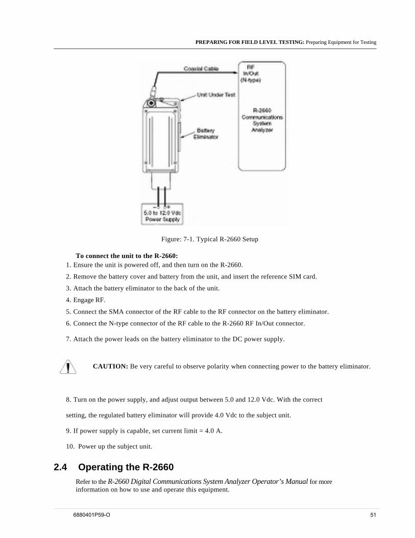
PREPARING FOR FIELD LEVEL TESTING: Preparing Equipment for Testing
Figure: 7-1. Typical R-2660 Setup
To connect the unit to the R-2660: 1. Ensure the unit is powered off, and then turn on the R-2660.
2. Remove the battery cover and battery from the unit, and insert the reference SIM card.
3. Attach the battery eliminator to the back of the unit.
4. Engage RF.
5. Connect the SMA connector of the RF cable to the RF connector on the battery eliminator.
6. Connect the N-type connector of the RF cable to the R-2660 RF In/Out connector.
7. Attach the power leads on the battery eliminator to the DC power supply.
CAUTION: Be very careful to observe polarity when connecting power to the battery eliminator.
8. Turn on the power supply, and adjust output between 5.0 and 12.0 Vdc. With the correct
setting, the regulated battery eliminator will provide 4.0 Vdc to the subject unit.
9. If power supply is capable, set current limit = 4.0 A.
10. Power up the subject unit.
2.4 Operating the R-2660 Refer to the R-2660 Digital Communications System Analyzer Operator’s Manual for more information on how to use and operate this equipment.
6880401P59-O 51
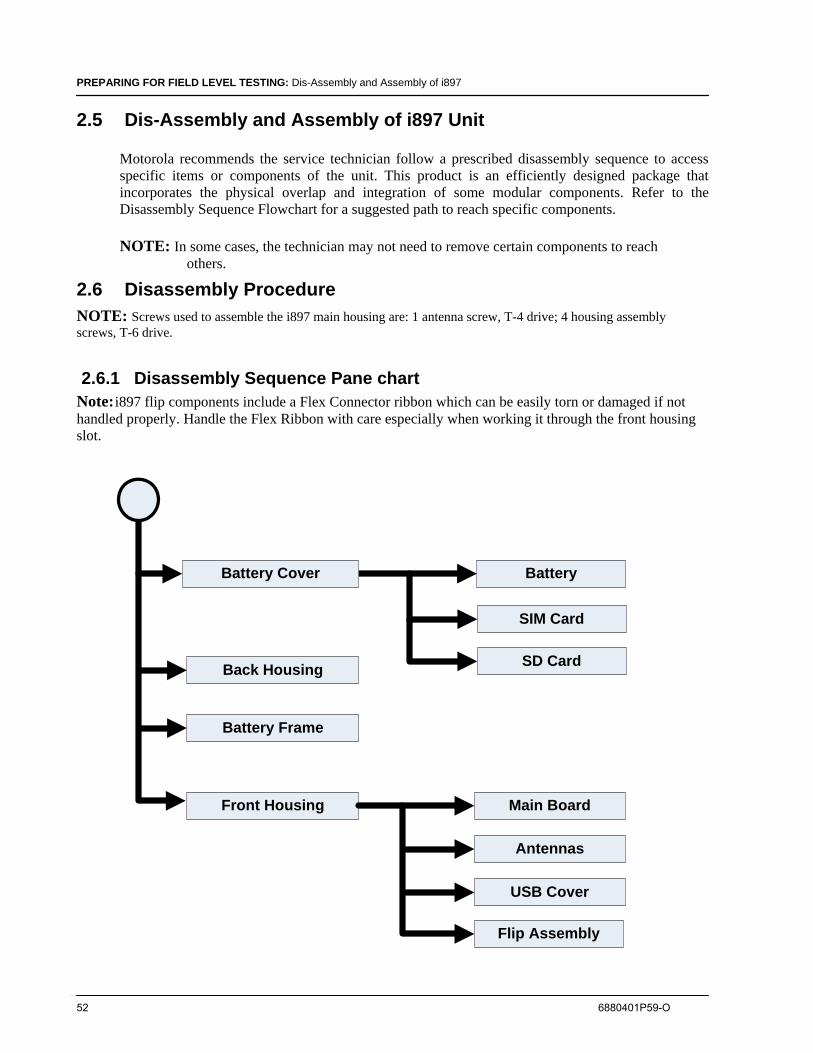
PREPARING FOR FIELD LEVEL TESTING: Dis-Assembly and Assembly of i897
2.5 Dis-Assembly and Assembly of i897 Unit
Motorola recommends the service technician follow a prescribed disassembly sequence to access specific items or components of the unit. This product is an efficiently designed package that incorporates the physical overlap and integration of some modular components. Refer to the Disassembly Sequence Flowchart for a suggested path to reach specific components.
NOTE: In some cases, the technician may not need to remove certain components to reach others.
2.6 Disassembly Procedure NOTE: Screws used to assemble the i897 main housing are: 1 antenna screw, T-4 drive; 4 housing assembly screws, T-6 drive.
2.6.1 Disassembly Sequence Pane chart Note: i897 flip components include a Flex Connector ribbon which can be easily torn or damaged if not handled properly. Handle the Flex Ribbon with care especially when working it through the front housing slot.
Main Board
Antennas
Back Housing
Front Housing
Battery Cover
SIM Card
Battery
USB Cover
Flip Assembly
SD Card
Battery Frame
52 6880401P59-O
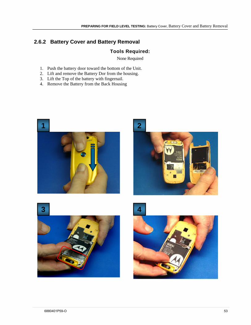
PREPARING FOR FIELD LEVEL TESTING: Battery Cover, Battery Cover and Battery Removal
2.6.2 Battery Cover and Battery Removal
Tools Required: None Required
1. Push the battery door toward the bottom of the Unit. 2. Lift and remove the Battery Dor from the housing. 3. Lift the Top of the battery with fingernail. 4. Remove the Battery from the Back Housing
1 2
3 4
6880401P59-O 53
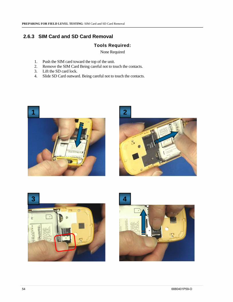
PREPARING FOR FIELD LEVEL TESTING: SIM Card and SD Card Removal
2.6.3 SIM Card and SD Card Removal
Tools Required: None Required
1. Push the SIM card toward the top of the unit. 2. Remove the SIM Card Being careful not to touch the contacts. 3. Lift the SD card lock. 4. Slide SD Card outward. Being careful not to touch the contacts.
1 2
3 4
54 6880401P59-O
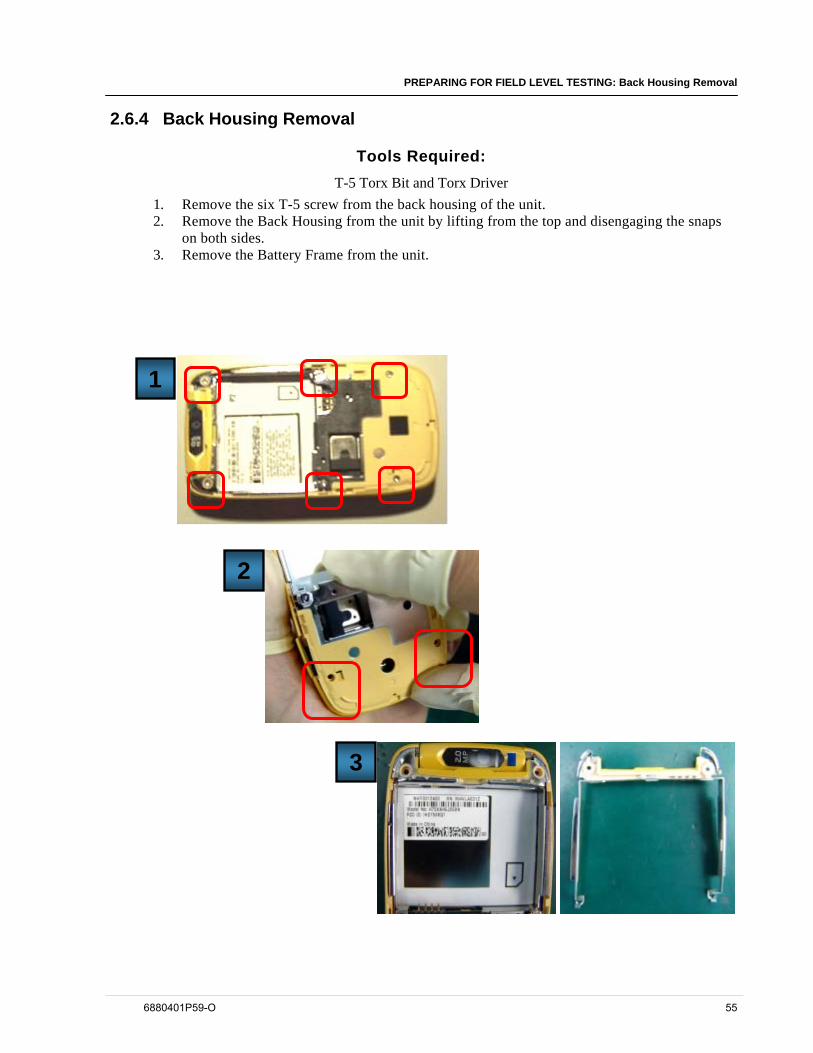
PREPARING FOR FIELD LEVEL TESTING: Back Housing Removal
2.6.4 Back Housing Removal
Tools Required: T-5 Torx Bit and Torx Driver
1. Remove the six T-5 screw from the back housing of the unit. 2. Remove the Back Housing from the unit by lifting from the top and disengaging the snaps
on both sides. 3. Remove the Battery Frame from the unit.
1
2
3
6880401P59-O 55
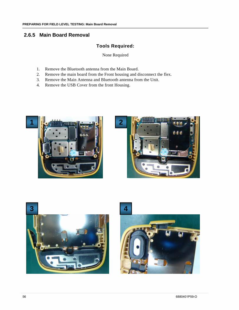
PREPARING FOR FIELD LEVEL TESTING: Main Board Removal
2.6.5 Main Board Removal
Tools Required:
None Required
1. Remove the Bluetooth antenna from the Main Board. 2. Remove the main board from the Front housing and disconnect the flex. 3. Remove the Main Antenna and Bluetooth antenna from the Unit. 4. Remove the USB Cover from the front Housing.
2 1
4 3
56 6880401P59-O
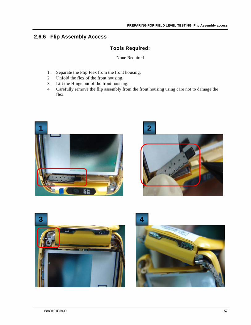
PREPARING FOR FIELD LEVEL TESTING: Flip Assembly access
2.6.6 Flip Assembly Access
Tools Required:
None Required
1. Separate the Flip Flex from the front housing. 2. Unfold the flex of the front housing. 3. Lift the Hinge out of the front housing. 4. Carefully remove the flip assembly from the front housing using care not to damage the
flex.
3 4
2 1
6880401P59-O 57

This page left blank intentionally
58 6880401P59-O
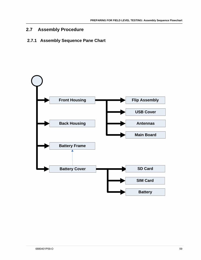
PREPARING FOR FIELD LEVEL TESTING: Assembly Sequence Flowchart
2.7 Assembly Procedure
2.7.1 Assembly Sequence Pane Chart
Main Board
AntennasBack Housing
Battery Frame
Battery Cover
SIM Card
Battery
USB Cover
Flip Assembly
SD Card
Front Housing
6880401P59-O 59
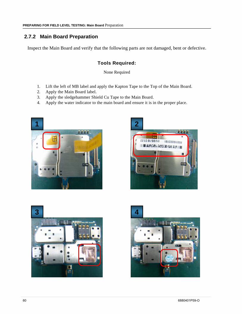
PREPARING FOR FIELD LEVEL TESTING: Main Board Preparation
2.7.2 Main Board Preparation
Inspect the Main Board and verify that the following parts are not damaged, bent or defective.
Tools Required:
None Required
1. Lift the left of MB label and apply the Kapton Tape to the Top of the Main Board. 2. Apply the Main Board label. 3. Apply the sledgehammer Shield Cu Tape to the Main Board. 4. Apply the water indicator to the main board and ensure it is in the proper place.
4 3
2 1
60 6880401P59-O
PREPARING FOR FIELD LEVEL TESTING: Main Board Preparation (Continued)
Main Board Preparation (Continued)
Tools Required:
None Required
5. Apply the Kapton tape to the SIM Strap on the main board. 6. Assemble USB strap to the Main Board. 7. Assemble the SIM card strap and Contact EMI shield to the main board and press it to
activate the adhesive. 8. Assemble two Contact EMI shield to the point of main board.
3
1
4
2
6880401P59-O 61
PREPARING FOR FIELD LEVEL TESTING: Flip to Front Housing Assembly
2.7.3 Flip to Front Housing Assembly
Tools Required: None Required
1. Apply the battery label in the battery cavity. 2. Apply 3 poron pads onto the front housing. 3. Apply a poron pad to the keypad Hinge Flex on the tip of the flex in the front housing. 4. Assemble the hinge button into the front housing with tweezers (Ensure proper direction)
as shown.
1 2
4 3
62 6880401P59-O
PREPARING FOR FIELD LEVEL TESTING: Flip to Front Housing Assembly (Continued)
Flip to Front Housing Assembly (Continued)
Tools Required: None Required
5. Assemble the ring in the FH. 6. Use the bottom of the tweezers to press the ring (Ensure the ridge of the ring is in the slot of
Front Housing correctly. 7. Insert the hinge mechanism into the flip housing. 8. Ensure correct orientation.
5 6
7 8
6880401P59-O 63
PREPARING FOR FIELD LEVEL TESTING: Flip to Front Housing Assembly (Continued)
Flip to Front Housing Assembly (Continued)
Tools Required:
None Required
9. Align the Flip with the ring in the Front Housing. 10. Align the hole on the hinge collar against the anchor point on the front housing, then close
the flip slowly. 11. Connect the Flex connector to the Front Housing Connector. 12. Apply the conductive poron on the location as shown.
9 10
11 12
64 6880401P59-O
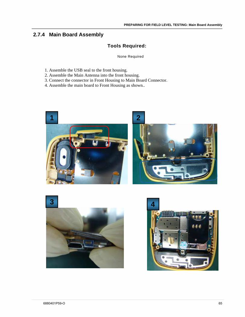
PREPARING FOR FIELD LEVEL TESTING: Main Board Assembly
2.7.4 Main Board Assembly
Tools Required:
None Required
1. Assemble the USB seal to the front housing. 2. Assemble the Main Antenna into the front housing. 3. Connect the connector in Front Housing to Main Board Connector. 4. Assemble the main board to Front Housing as shown..
1 2
3 4
6880401P59-O 65
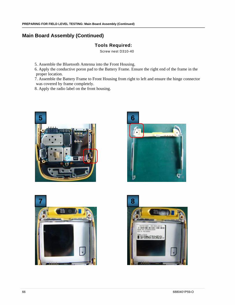
PREPARING FOR FIELD LEVEL TESTING: Main Board Assembly (Continued)
Main Board Assembly (Continued)
Tools Required: Screw nest D310-40
5. Assemble the Bluetooth Antenna into the Front Housing. 6. Apply the conductive poron pad to the Battery Frame. Ensure the right end of the frame in the proper location.
7. Assemble the Battery Frame to Front Housing from right to left and ensure the hinge connector was covered by frame completely.
8. Apply the radio label on the front housing.
5 6
7 8
66 6880401P59-O
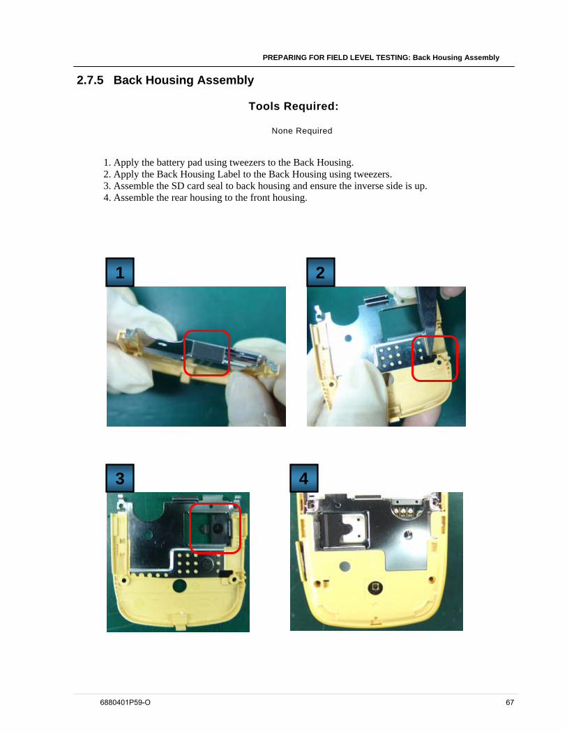
PREPARING FOR FIELD LEVEL TESTING: Back Housing Assembly
2.7.5 Back Housing Assembly
Tools Required:
None Required
1. Apply the battery pad using tweezers to the Back Housing. 2. Apply the Back Housing Label to the Back Housing using tweezers. 3. Assemble the SD card seal to back housing and ensure the inverse side is up. 4. Assemble the rear housing to the front housing.
1 2
3 4
6880401P59-O 67
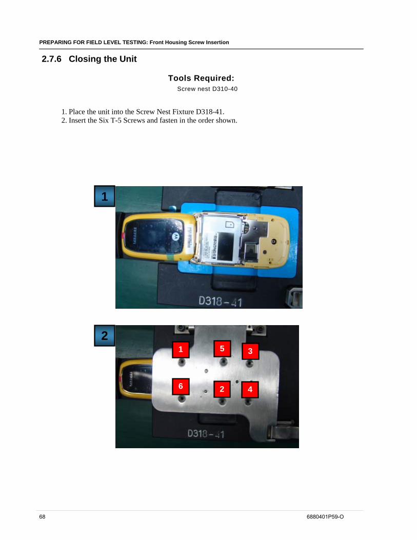
PREPARING FOR FIELD LEVEL TESTING: Front Housing Screw Insertion
2.7.6 Closing the Unit
Tools Required: Screw nest D310-40
1. Place the unit into the Screw Nest Fixture D318-41. 2. Insert the Six T-5 Screws and fasten in the order shown.
1
2 5 1 3
6 2 4
68 6880401P59-O
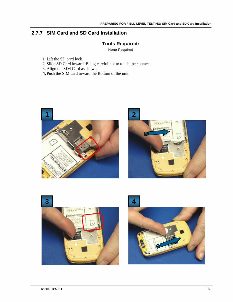
PREPARING FOR FIELD LEVEL TESTING: SIM Card and SD Card Installation
2.7.7 SIM Card and SD Card Installation
Tools Required: None Required
1. Lift the SD card lock. 2. Slide SD Card inward. Being careful not to touch the contacts. 3. Align the SIM Card as shown 4. Push the SIM card toward the Bottom of the unit.
3 4
1 2
6880401P59-O 69
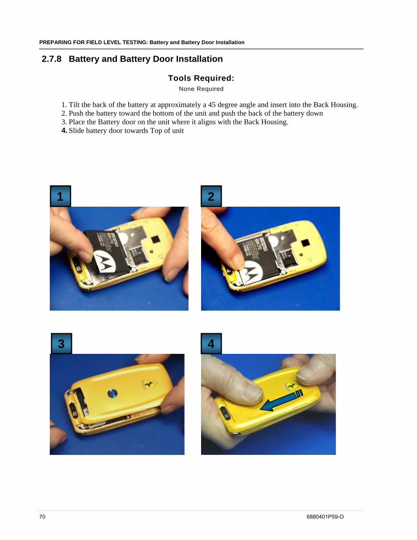
PREPARING FOR FIELD LEVEL TESTING: Battery and Battery Door Installation
2.7.8 Battery and Battery Door Installation
Tools Required: None Required
1. Tilt the back of the battery at approximately a 45 degree angle and insert into the Back Housing. 2. Push the battery toward the bottom of the unit and push the back of the battery down 3. Place the Battery door on the unit where it aligns with the Back Housing. 4. Slide battery door towards Top of unit
1 2
3 4
70 6880401P59-O
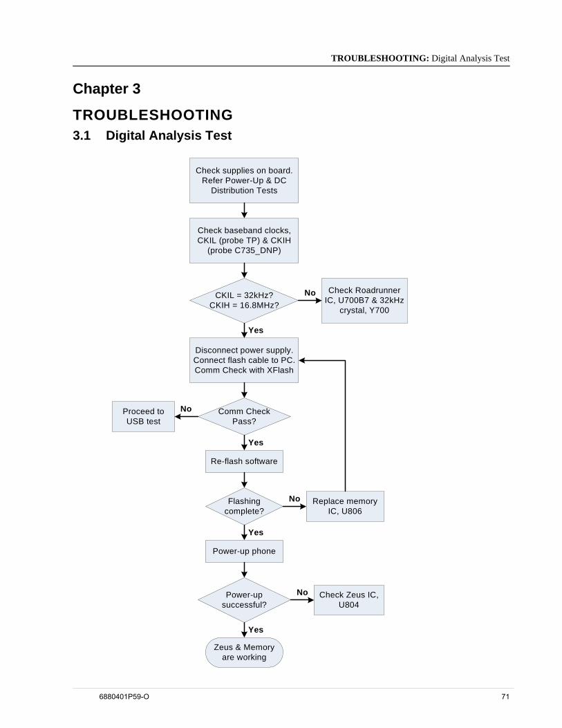
TROUBLESHOOTING: Digital Analysis Test
Chapter 3
TROUBLESHOOTING 3.1 Digital Analysis Test
Check supplies on board. Refer Power-Up & DC
Distribution Tests
Check baseband clocks, CKIL (probe TP) & CKIH
(probe C735_DNP)
CKIL = 32kHz?CKIH = 16.8MHz?
Check Roadrunner IC, U700B7 & 32kHz
crystal, Y700
Disconnect power supply. Connect flash cable to PC. Comm Check with XFlash
Comm Check Pass?
Re-flash software
Proceed to USB test
Flashing complete?
Power-up phone
Replace memory IC, U806
Power-up successful?
Zeus & Memory are working
Check Zeus IC, U804
Yes
Yes
Yes
Yes
No
No
No
No
6880401P59-O 71
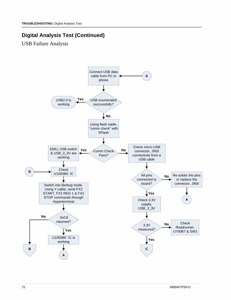
TROUBLESHOOTING: Digital Analysis Test
Digital Analysis Test (Continued)
USB Failure Analysis
Check micro-USB connector, J900
connectivity from a USB cable
All pins connected to
board?
Re-solder the pins or replace the
connector, J900
Using flash cable, “comm check” with
XFlash
Comm Check Pass?
Yes
No
EMU, USB switch & USB_3_3V are
working
Switch into Berbug mode. Using Y-cable, send FX2
START, FX2 REG 1 & FX2 STOP commands through
Hyperterminal
0xC8 returned?
USB enumerated successfully?
Connect USB data cable from PC to
phone
No
No
A
A
USB2.0 is working
Yes
Yes
Check 3.3V supply,
USB_3_3V
3.3V measured?
C
Yes
No
A
Yes
No
B
D
Check Roadrunner,
U700B7 & SW3
Check U1000B6 IC
U1000B6 IC is working
72 6880401P59-O
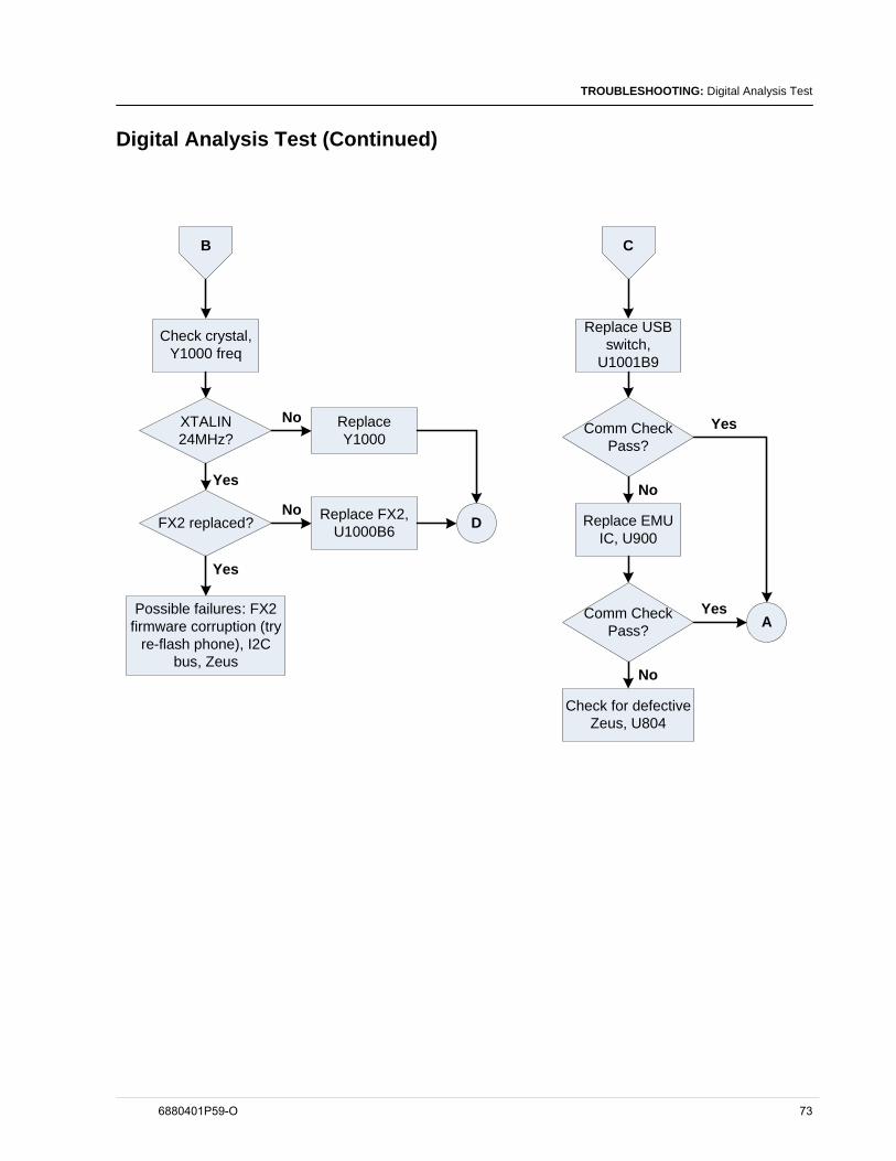
TROUBLESHOOTING: Digital Analysis Test
Digital Analysis Test (Continued)
Replace USB switch,
U1001B9
Comm Check Pass?
Replace EMU IC, U900
Comm Check Pass?
Check for defective Zeus, U804
Yes
Yes
No
No
C
A
Replace FX2, U1000B6
B
Check crystal, Y1000 freq
XTALIN 24MHz?
Replace Y1000
D
Possible failures: FX2 firmware corruption (try
re-flash phone), I2C bus, Zeus
FX2 replaced?
Yes
Yes
No
No
6880401P59-O 73
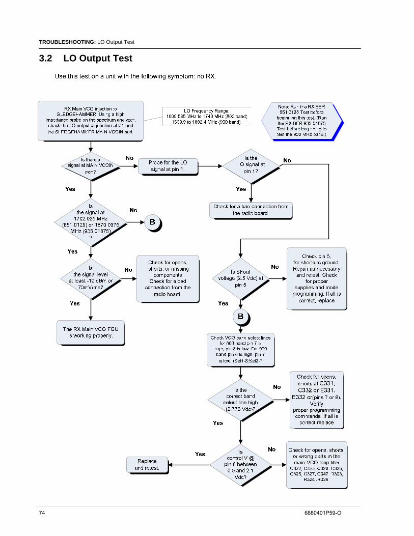
TROUBLESHOOTING: LO Output Test
3.2 LO Output Test
74 6880401P59-O
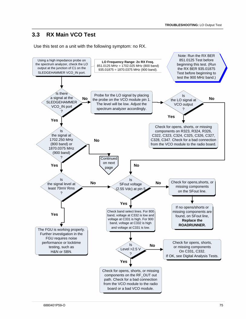
TROUBLESHOOTING: LO Output Test
3.3 RX Main VCO Test
Use this test on a unit with the following symptom: no RX.
Is therea signal at the
SLEDGEHAMMERVCO_IN port
?
Using a high impedance probe onthe spectrum analyzer, check the LO
output at the junction of C1 on theSLEDGEHAMMER VCO_IN port.
Probe for the LO signal by placing the probe on the VCO module pin 1.
The level will be low. Adjust the spectrum analyzer accordingly.
Check for opens,shorts, or missing components
on the SFout line.
Check band select lines. For 800band, voltage at C332 is low andvoltage at C331 is high. For 900
band, voltage at C332 is highand voltage at C331 is low.
Check for opens, shorts, or missingcomponents on the RF_OUT outpath. Check for a bad connectionfrom the VCO module to the radio
board or a bad VCO module.
The FGU is working properly. Further investigation in the
FGU requires noise performance or locktime
testing, such asH&N or SBN.
Check for opens, shorts, or missingcomponents on R323, R324, R326,
C322, C323, C324, C325, C326, C327, C328, C347. Check for a bad connection from the VCO module to the radio board.
Yes
No
IsLevel >2.5 V
?
Isthe LO signal at
VCO output?
IsSFout voltage
(2.55 Vdc) at pin 5
Isthe signal level atleast 70mV Rms
?
Isthe signal at
1702.250 MHz(800 band) or
1870.0375 MHz(900 band)
?
Check for opens, shorts,or missing components
On C331, C332. If OK, see Digital Analysis Tests.
Yes
No
Yes
No
Note: Run the RX BER 851.0125 Test before
beginning this test. (Run the RX BER 935.01875 Test before beginning to test the 900 MHz band.)
LO Frequency Range: 2x RX Freq. 851.0125 MHz = 1702.025 MHz (800 band) 935.01875 = 1870.0375 MHz (900 band).
No
NoNo
No
Yes
Yes
Yes
Continuedon next page
If no opens/shorts ormissing components are
found, on SFout line,Replace the
ROADRUNNER.
6880401P59-O 75
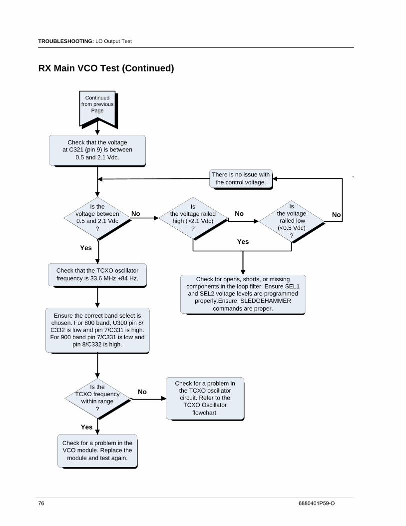
TROUBLESHOOTING: LO Output Test
RX Main VCO Test (Continued)
Is thevoltage between0.5 and 2.1 Vdc
?
Check that the voltageat C321 (pin 9) is between
0.5 and 2.1 Vdc.
Check that the TCXO oscillatorfrequency is 33.6 MHz +84 Hz.
There is no issue withthe control voltage.
Ensure the correct band select is chosen. For 800 band, U300 pin 8/C332 is low and pin 7/C331 is high. For 900 band pin 7/C331 is low and
pin 8/C332 is high.
Check for a problem inthe TCXO oscillatorcircuit. Refer to the
TCXO Oscillatorflowchart.
Check for a problem in theVCO module. Replace the
module and test again.
Yes
NoIs
the voltagerailed low
(<0.5 Vdc)?
Is theTCXO frequency
within range?
Isthe voltage railedhigh (>2.1 Vdc)
?
No
Yes
No
Yes
Check for opens, shorts, or missingcomponents in the loop filter. Ensure SEL1 and SEL2 voltage levels are programmed
properly.Ensure SLEDGEHAMMER commands are proper.
Continued from previous
Page
No
‘
76 6880401P59-O
TROUBLESHOOTING: Keypad Failure Test
3.4 Keypad Failure Test.
6880401P59-O 77
TROUBLESHOOTING: SLEDGEHAMMER Test
3.5 SLEDGEHAMMER Test
Is thevoltage at R660
2.775 Vdc(SF)
Go to thetest flowcharts forvoltage regulator
verification.
CheckL653 for
2.775 Vdc (V2_RX).
Go to thetest flowcharts forvoltage regulator
verification.
Yes
No
Isthe voltage
at L653correct +10%
?
Is thevoltage at E601
and R325 at 1.875Vdc
+10%?
Yes
No
Is thevoltage at E659(SF) at 2.56 Vdc
+10%
The problem is in theSLEDGEHAMMER.Repair or replace, as
necessary.
Go to thetest flowcharts forvoltage regulator
verification.
Use this test to check the SLEDGEHAMMER circuitry.
Yes
No
Yes
No
Continuedon next page
78 6880401P59-O
TROUBLESHOOTING: SLEDGEHAMMER Test
SLEDGEHAMMER Test (Continued)
Isthe voltage
at C332~ 0 Vdc and voltage at
C331 ~ 2.775 Vdc?
Remove U200, and check
the voltage again.
1. In BERBUG, type thefollowing: >rx static>mode rx (Ignore themessage returned).2. Check the voltageon C332 and C331.
The SLEDGEHAMMERis functional.
Yes
No
Is thevoltage at C332
~ 0 Vdc and voltage atC331 ~ 2.775 Vdc?
ReplaceROADRUNNER IC.
The problem is in theVCO module. Replacethe module and run the
test again.
Yes
No
6880401P59-O 79
TROUBLESHOOTING: RX Analysis Test
3.6 RX Analysis Test
Use this test on a unit to perform a RX analysis in iDEN mode.1. Set up the R-2660 as follows: Mode: iDEN Test, Meter: RF DISPLAY, RF Control: GENERATE, FREQ: (SeeTable) MHz, Gen: OUT6/6, Gen: -60 dBm, RF I/O.2. Set the spectrum analyzer to Center Freq: 851.000 MHz (935.01875 MHz for 900), Span: 100 kHz, Amplitude:-30 dBm reference level. Set marker to test frequency, and use Trace and Max. Hold to obtain readings. Use Clearbefore taking each reading.3. Except as noted, use a 50-ohm probe for all RF measurements. The probe ground must make contact with theboard ground during the measurements.4. Check that signal measurement levels are +3dB at each test point, unless otherwise stated. A low RSSI level willresult in higher BER as the signal becomes weaker.5. The RF cable from the R-2660 to the unit under test (UUT) should be <18 in. for these measurements in this flowchart.6. Be sure to check for any defects, such as unsoldered connections, shorts, broken or defective components.7. Remove the antenna from the UUT before beginning these tests.
Do voltagesagree withtable +5%?
Inject a -50 dBm CW tone into the RF jack at the selected frequency from the table with a frequency offset (+ 2KHz).
Place Radio into BERBUG, and send the following commands: RX STATICRX FREQ XXX ( XXX is one of the
frequencies from the table) MODE RX
For the programmed frequency, measure voltages on the capacitors in the table.
Check R760, R759, R758 for S,US, MP and DFP then if no fault remove the three resistors from the board and measure
the voltages on the Roadrunner side of the resistor.
Yes
NoWere all
frequencies fromtable tested?
Yes
No
Abbreviations:S - check for ShortsUS - check for unsoldered parts / open connections MP - check for missing partsDFP - check for defective parts
Do voltages
agree with table +5%?
Check the voltages on positive terminal of C212
( negative terminal always 0V)
Check R760, R759, R758 for S, DFP.
Check DC section, then if no fault found replace the
Roadrunner IC (U700).
Frequency GP03- GP04- GP05-(MHz) R760 R759 R758
Voltage Voltage Voltage860 0 2.775 2.775915.525 2.775 0 0937.49375 2.775 0 2.775
No
Are voltages2.775 V +5%?
Check C212, R212 and C214 for S, DFP.Check DC section, then if no fault
found replace the Janus Module (U500).
Yes
Check DC section, then if no fault found replace the
Roadrunner IC (U700).
No
Measure DC voltages on TP_RXI, TP_RXIX, TP_RXQ, TP_RXQX.
Yes
A
Continuedon next page
80 6880401P59-O
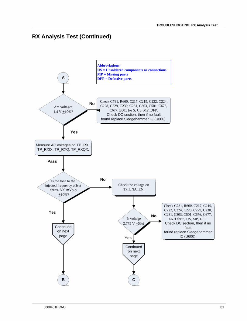
TROUBLESHOOTING: RX Analysis Test
RX Analysis Test (Continued)
Is the tone to the injected frequency offset
aprox. 500 mVp-p +10%?
Check C781, R660, C217, C219, C222, C224, C228, C229, C230, C231, C303, C501, C676,
C677, E601 for S, US, MP, DFP.Check DC section, then if no fault
found replace Sledgehammer IC (U600).
Are voltages 1.4 V +10%?
Check the voltage on TP_LNA_EN.
Yes
No
Abbreviations:US = Unsoldered components or connectionsMP = Missing partsDFP = Defective parts
Continuedon next page
Yes
Pass
No
A
Measure AC voltages on TP_RXI, TP_RXIX, TP_RXQ, TP_RXQX.
B
Is voltage 2.775 V +5%?
Continuedon next page
C
Yes
Check C781, R660, C217, C219, C222, C224, C228, C229, C230, C231, C303, C501, C676, C677,
E601 for S, US, MP, DFP.Check DC section, then if no
fault found replace Sledgehammer
IC (U600).
No
6880401P59-O 81
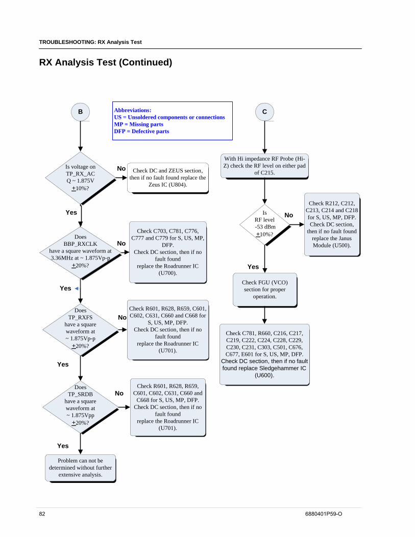
TROUBLESHOOTING: RX Analysis Test
RX Analysis Test (Continued)
DoesTP_RXFS
have a squarewaveform at~ 1.875Vp-p
+20%?
Check DC and ZEUS section,then if no fault found replace the
Zeus IC (U804).
Is voltage onTP_RX_ACQ ~ 1.875V
+10%?
DoesBBP_RXCLK
have a square waveform at3.36MHz at ~ 1.875Vp-p
+20%?
Yes
No
Abbreviations:US = Unsoldered components or connectionsMP = Missing partsDFP = Defective parts
Yes
No
Yes
No
DoesTP_SRDB
have a squarewaveform at~ 1.875Vpp
+20%?
Yes
Check R601, R628, R659, C601, C602, C631, C660 and
C668 for S, US, MP, DFP.Check DC section, then if no
fault foundreplace the Roadrunner IC
(U701).
Check R601, R628, R659, C601, C602, C631, C660 and C668 for
S, US, MP, DFP.Check DC section, then if no
fault foundreplace the Roadrunner IC
(U701).
Check C703, C781, C776, C777 and C779 for S, US, MP,
DFP.Check DC section, then if no
fault foundreplace the Roadrunner IC
(U700).
Problem can not be determined without further
extensive analysis.
No
B C
With Hi impedance RF Probe (Hi-Z) check the RF level on either pad
of C215.
Is RF level -53 dBm +10%?
Check FGU (VCO) section for proper
operation.
Check R212, C212, C213, C214 and C218 for S, US, MP, DFP.Check DC section,
then if no fault found replace the Janus Module (U500).
Yes
No
Check C781, R660, C216, C217, C219, C222, C224, C228, C229, C230, C231, C303, C501, C676, C677, E601 for S, US, MP, DFP.
Check DC section, then if no fault found replace Sledgehammer IC
(U600).
82 6880401P59-O
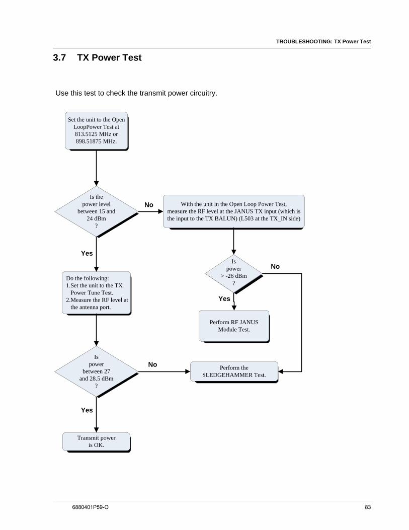
TROUBLESHOOTING: TX Power Test
3.7 TX Power Test
Use this test to check the transmit power circuitry.
With the unit in the Open Loop Power Test,
measure the RF level at the JANUS TX input (which is the input to the TX BALUN) (L503 at the TX_IN side)
Do the1.Set
following:the unit to the TX
Power Tune Test.2.Measure the RF level at the antenna port.
Transmit poweris OK.
Is thepower level
between 15 and24 dBm
?
Yes
Yes
No
Yes
No
Perform theSLEDGEHAMMER Test.
NoIs
power> -26 dBm
?
Perform RF JANUSModule Test.
Set the unit to the OpenLoopPower Test at813.5125 MHz or898.51875 MHz.
Ispower
between 27and 28.5 dBm
?
6880401P59-O 83
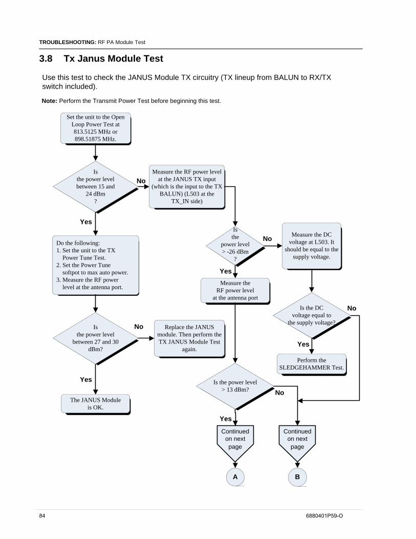
TROUBLESHOOTING: RF PA Module Test
3.8 Tx Janus Module Test
Note: Perform the Transmit Power Test before beginning this test.
Use this test to check the JANUS Module TX circuitry (TX lineup from BALUN to RX/TX switch included).
Measure the RF power level at the JANUS TX input
(which is the input to the TX BALUN) (L503 at the
TX_IN side)
Do the following:1. Set the unit to the TX Power Tune Test.2. Set the Power Tune softpot to max auto power.3. Measure the RF power level at the antenna port.
The JANUS Moduleis OK.
Isthe power levelbetween 15 and
24 dBm?
Yes
Yes
No
Yes
No
Measure the DC voltage at L503. It
should be equal to the supply voltage.
No
Isthe
power level> -26 dBm
?
Replace the JANUS module. Then perform the TX JANUS Module Test
again.
Set the unit to the Open Loop Power Test at 813.5125 MHz or898.51875 MHz.
Isthe power level
between 27 and 30dBm?
Measure theRF power level
at the antenna port
Continuedon next page
Is the DC voltage equal to
the supply voltage?
Perform theSLEDGEHAMMER Test.
Yes
Is the power level > 13 dBm?
Yes
Continuedon next page
No
A B
No
84 6880401P59-O
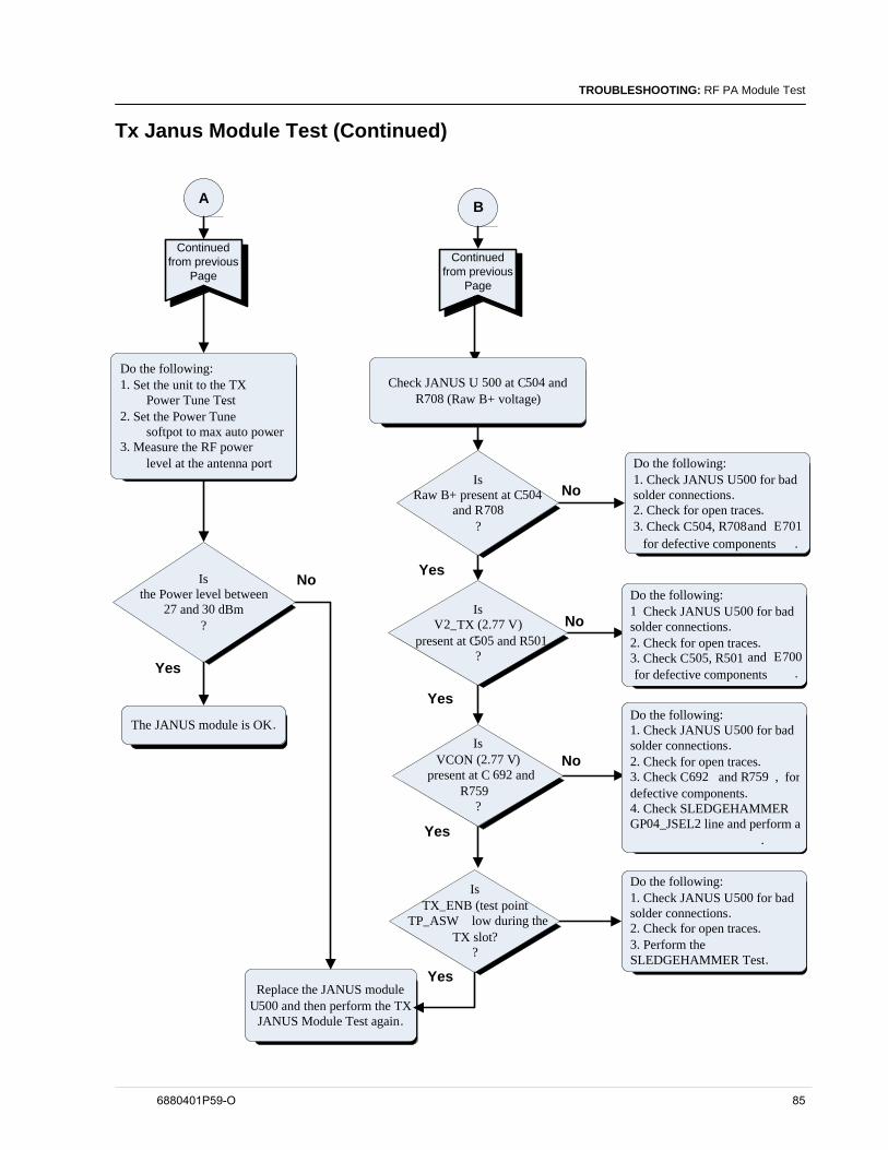
TROUBLESHOOTING: RF PA Module Test
Tx Janus Module Test (Continued)
A B
Continued from previous
Page
Continued from previous
Page
and Check JANUS U 500 R708 (Raw B+
at C504 voltage)
The JANUS module is OK.
Yes
Is the Power level between
27 and 30 dBm ?
Yes
No
No
No
Do the following:1 . Check JANUS U500 for bad solder connections.2 . Check for open traces.3 . Check C692 and R759 , for defective components.4 . Check SLEDGEHAMMER
2 line and perform a .
_ JSELGP
04
IsRaw B+ present at C504
and R708?
No
Do the following:1 . Check JANUS U500 for bad solder connections.2 . Check for open traces.3 . Check C504 , R708 E701 and for defective components .
Yes
Yes
700 .
E
Do the following:1 Check JANUS U500 for bad solder connections.2 . Check for open traces.3 . Check C505 , R501 for defective components
and
IsV2_TX (2.77 V)
present at C505 and R501?
Yes
IsVCON (2.77 V)
present at C 692 and R759
?
Replace the JANUS module U500 and then perform the TX
.
Do the following:1 . Check JANUS U500 for bad solder connections.2 . Check for open traces.3 . Perform the SLEDGEHAMMER Test
IsTX_ENB (test point
TP_ASW low during the TX slot
??
.JANUS Module Test again
Do the following: 1 . Set the unit to the TX Power Tune T tes. 2 . Set the Power Tune softpot to max auto pow r e. 3 . Measure the RF power level at the antenna port.
6880401P59-O 85
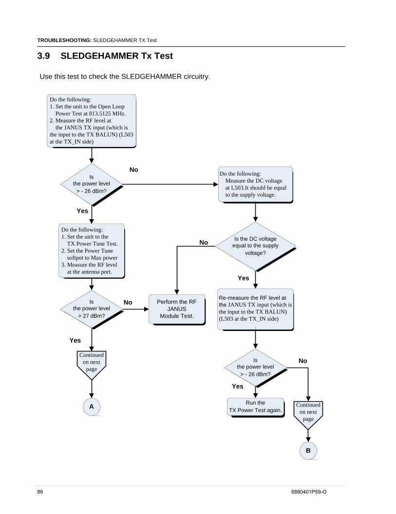
TROUBLESHOOTING: SLEDGEHAMMER TX Test
3.9 SLEDGEHAMMER Tx Test
Use this test to check the SLEDGEHAMMER circuitry.
Do the following: Measure the DC voltage at L503.It should be equal to the supply voltage.
Isthe power level
> - 26 dBm?
Yes
No
Yes
No
No
Run theTX Power Test again.
No
Yes
Perform the RF JANUS
Module Test.
Do the following:1. Set the unit to the Open Loop Power Test at 813.5125 MHz.2. Measure the RF level at the JANUS TX input (which is the input to the TX BALUN) (L503 at the TX_IN side)
Re-measure the RF level at the JANUS TX input (which is the input to the TX BALUN) (L503 at the TX_IN side)
.
Isthe power level
> 27 dBm?
Do the following:1. Set the unit to the TX Power Tune Test.2. Set the Power Tune softpot to Max power3. Measure the RF level at the antenna port.
Is the DC voltageequal to the supply
voltage?
Isthe power level
> - 26 dBm?
Continuedon next
page
Yes
Continuedon next
page
A
B
86 6880401P59-O
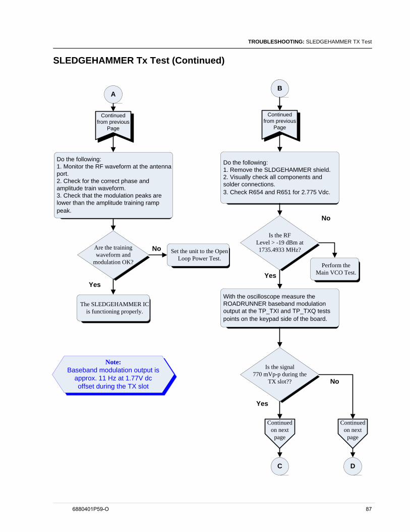
TROUBLESHOOTING: SLEDGEHAMMER TX Test
SLEDGEHAMMER Tx Test (Continued)
Are the training waveform and
modulation OK?
Yes
No
Do the following:1. Monitor the RF waveform at the antenna port.2. Check for the correct phase and amplitude train waveform.3. Check that the modulation peaks are lower than the amplitude training ramp peak.
Set the unit to the Open Loop Power Test.
Continuedon next
page
Continued from previous
Page
The SLEDGEHAMMER IC is functioning properly.
Note: Baseband modulation output is
approx. 11 Hz at 1.77V dc offset during the TX slot
AB
Continued from previous
Page
Do the following:1. Remove the SLDGEHAMMER shield.2. Visually check all components and solder connections.3. Check R654 and R651 for 2.775 Vdc.
Is the RF Level > -19 dBm at 1735.4933 MHz?
With the oscilloscope measure the ROADRUNNER baseband modulation output at the TP_TXI and TP_TXQ tests points on the keypad side of the board.
Yes
Is the signal 770 mVp-p during the
TX slot??
Yes
C
Perform the Main VCO Test.
No
D
No
Continuedon next
page
6880401P59-O 87
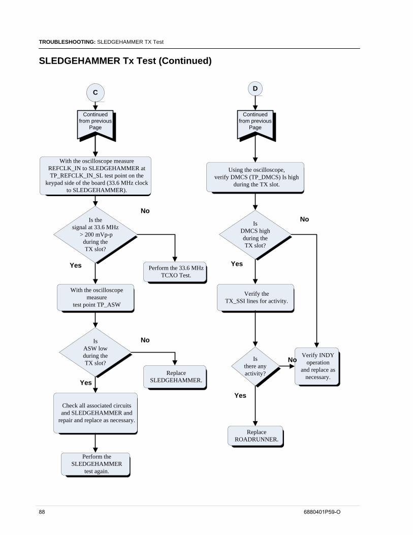
TROUBLESHOOTING: SLEDGEHAMMER TX Test
SLEDGEHAMMER Tx Test (Continued)
Continued from previous
Page
IsDMCS highduring theTX slot?
Verify INDYoperation
and replace asnecessary.
Verify theTX_SSI lines for activity.
ReplaceROADRUNNER.
Is ASW lowduring theTX slot?
No
With the oscilloscope measure REFCLK_IN to SLEDGEHAMMER at TP_REFCLK_IN_SL test point on the
keypad side of the board (33.6 MHz clock to SLEDGEHAMMER).
Perform theSLEDGEHAMMER
test again.
With the oscilloscopemeasure
test point TP_ASW
Check all associated circuitsand SLEDGEHAMMER and
repair and replace as necessary.
Isthere anyactivity?Replace
SLEDGEHAMMER.
Perform the 33.6 MHzTCXO Test.
Is thesignal at 33.6 MHz
> 200 mVp-pduring theTX slot?
Yes
No
Yes
No
Yes
No
C D
Using the oscilloscope, verify DMCS (TP_DMCS) Is high
during the TX slot.
Yes
Continued from previous
Page
88 6880401P59-O
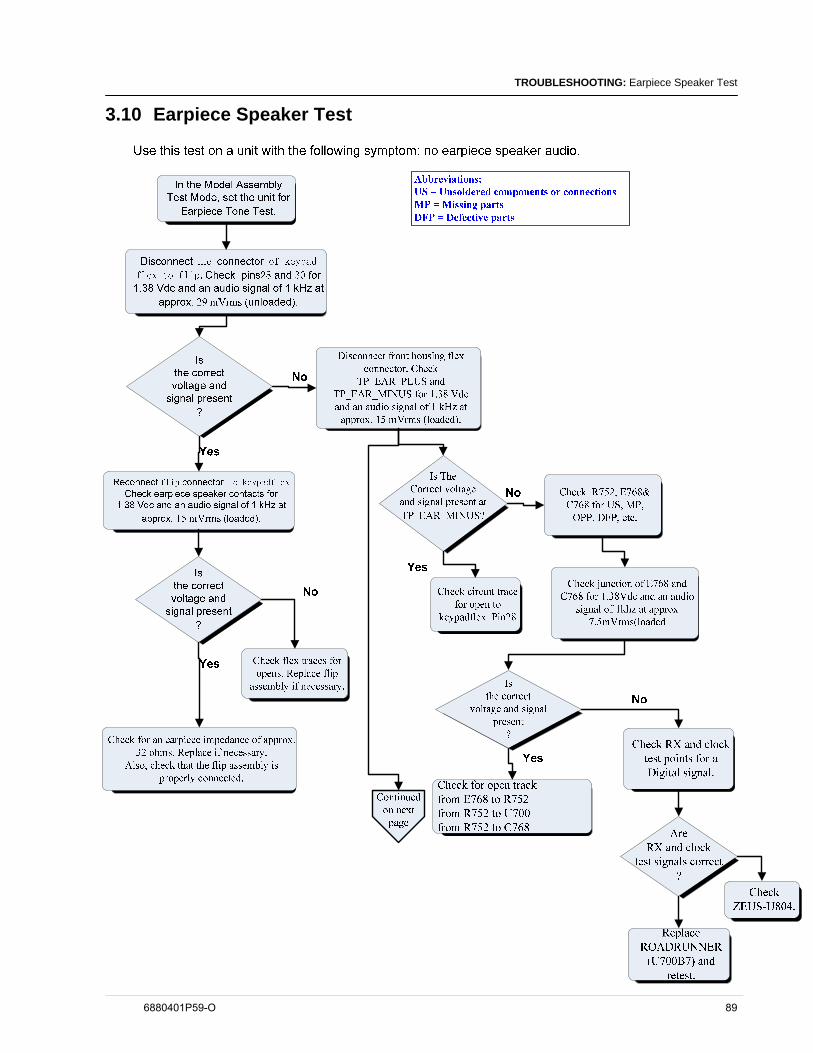
TROUBLESHOOTING: Earpiece Speaker Test
3.10 Earpiece Speaker Test
6880401P59-O 89
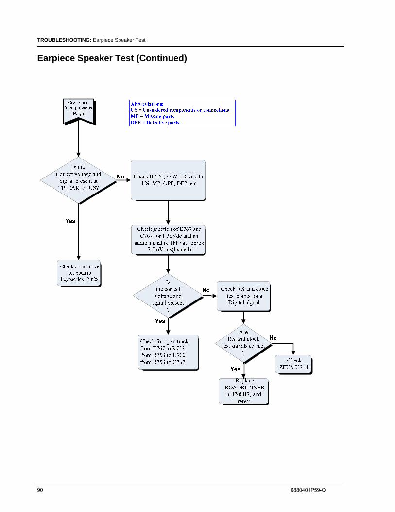
TROUBLESHOOTING: Earpiece Speaker Test
Earpiece Speaker Test (Continued)
90 6880401P59-O
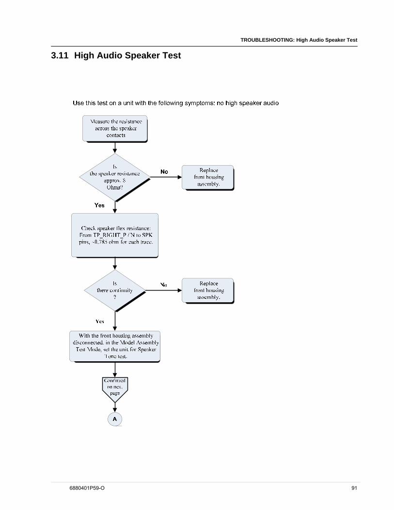
TROUBLESHOOTING: High Audio Speaker Test
3.11 High Audio Speaker Test
6880401P59-O 91
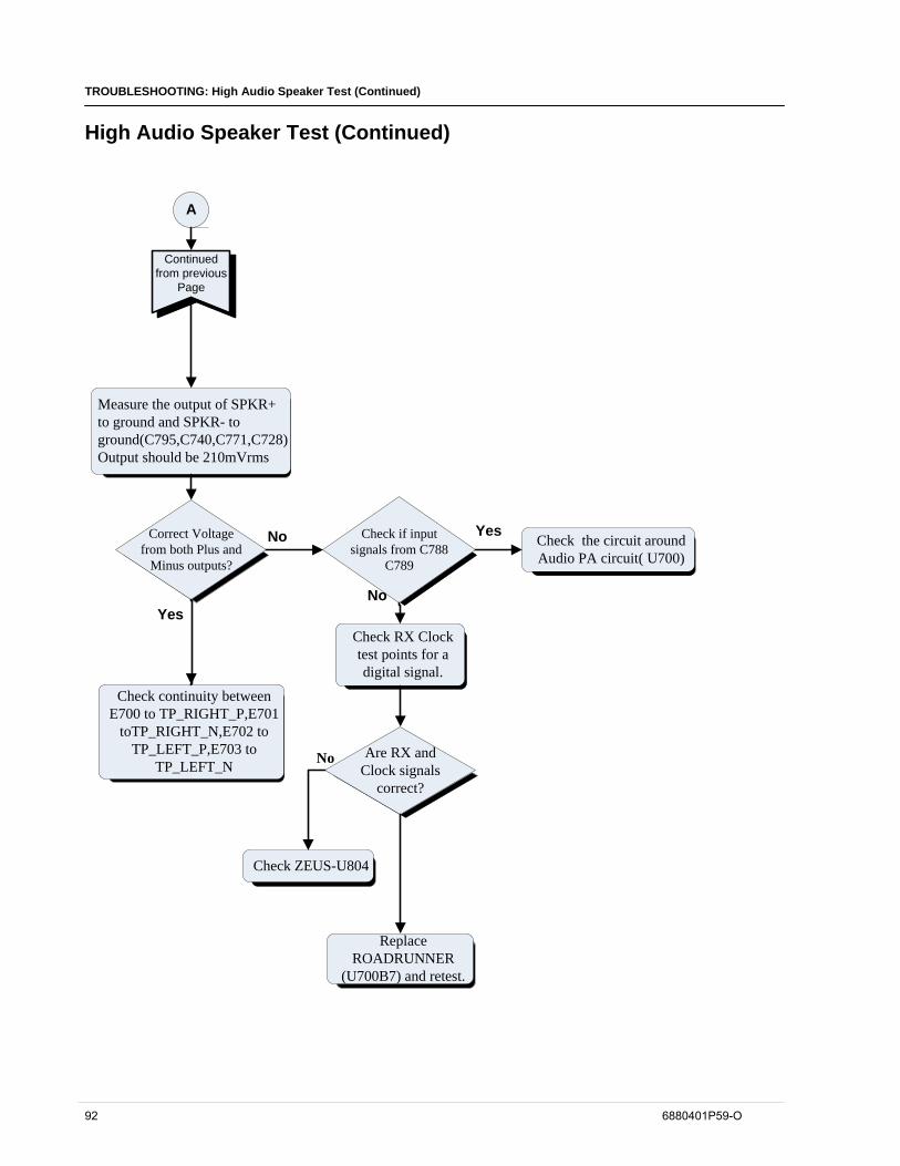
TROUBLESHOOTING: High Audio Speaker Test (Continued)
High Audio Speaker Test (Continued)
No
Measure the output of SPKR+ to ground and SPKR- to ground(C795,C740,C771,C728)Output should be 210mVrms
Check continuity between E700 to TP_RIGHT_P,E701
toTP_RIGHT_N,E702 to TP_LEFT_P,E703 to
TP_LEFT_N
Correct Voltagefrom both Plus and
Minus outputs?
Yes
Check the circuit around Audio PA circuit( U700)
Continued from previous
Page
A
Check if input signals from C788
C789
No
Yes
Check RX Clock test points for a digital signal.
Are RX andClock signals
correct?
ReplaceROADRUNNER
(U700B7) and retest.
No
Check ZEUS-U804
92 6880401P59-O
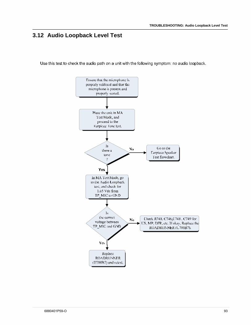
TROUBLESHOOTING: Audio Loopback Level Test
3.12 Audio Loopback Level Test
6880401P59-O 93
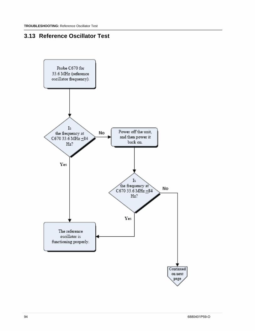
TROUBLESHOOTING: Reference Oscillator Test
3.13 Reference Oscillator Test
94 6880401P59-O
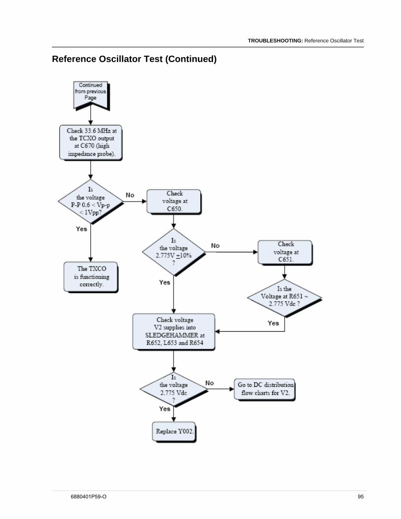
TROUBLESHOOTING: Reference Oscillator Test
Reference Oscillator Test (Continued)
6880401P59-O 95
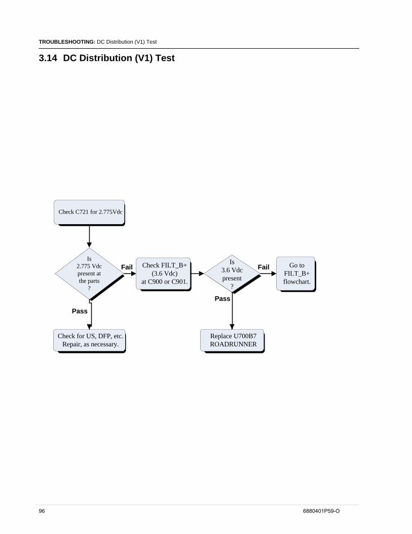
TROUBLESHOOTING: DC Distribution (V1) Test
3.14 DC Distribution (V1) Test
Check C721 for 2.775Vdc
Check for US, DFP, etc.Repair, as necessary.
Is2.775 Vdcpresent atthe parts
?
Check FILT_B+(3.6 Vdc)
at C900 or C901.
Go toFILT_B+flowchart.
Is3.6 Vdcpresent
?
Replace U700B7ROADRUNNER
Fail
Pass
Pass
Fail
96 6880401P59-O
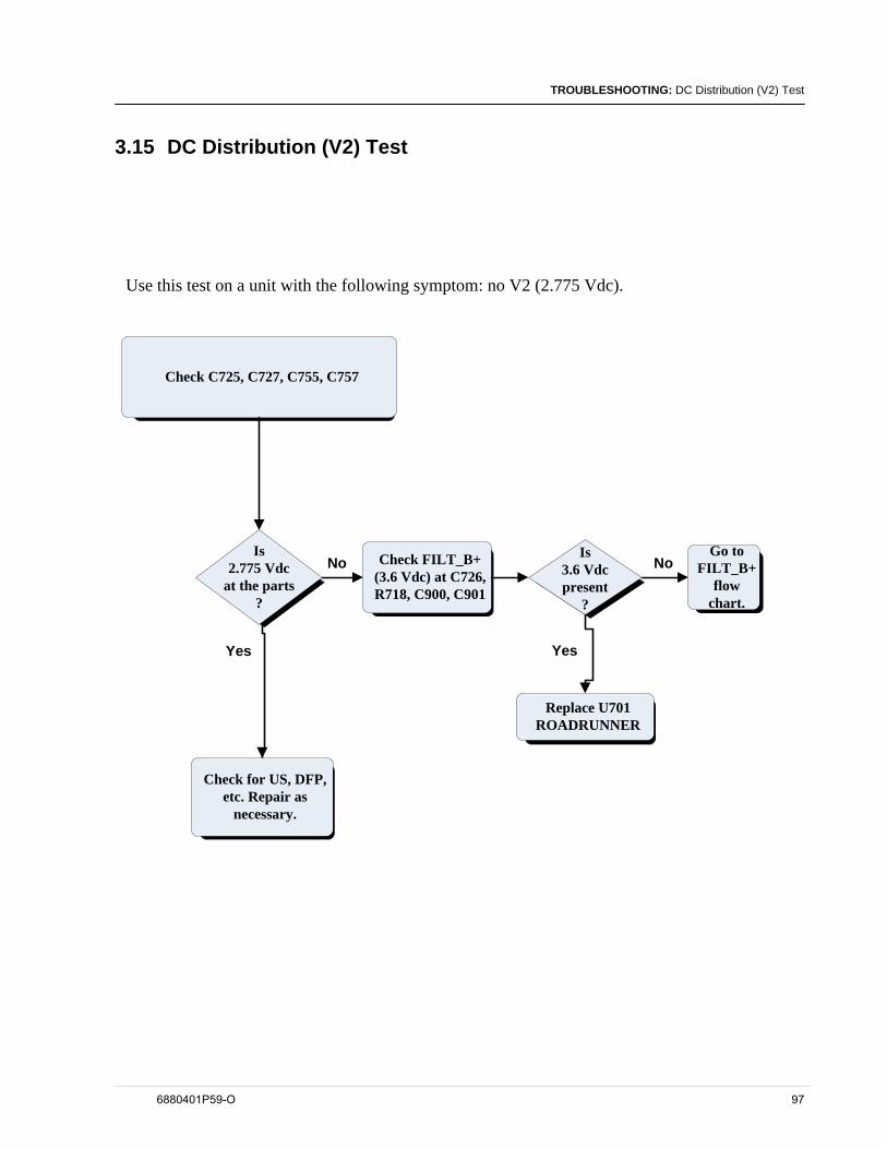
TROUBLESHOOTING: DC Distribution (V2) Test
3.15 DC Distribution (V2) Test
No
Check C725, C727, C755, C757
Go to FILT_B+
flow chart.
Is2.775 Vdc
at the parts?
Check FILT_B+ (3.6 Vdc) at C726, R718, C900, C901
Is3.6 Vdcpresent
?
No
YesYes
Check for US, DFP,etc. Repair as
necessary.
Replace U701ROADRUNNER
Use this test on a unit with the following symptom: no V2 (2.775 Vdc).
6880401P59-O 97
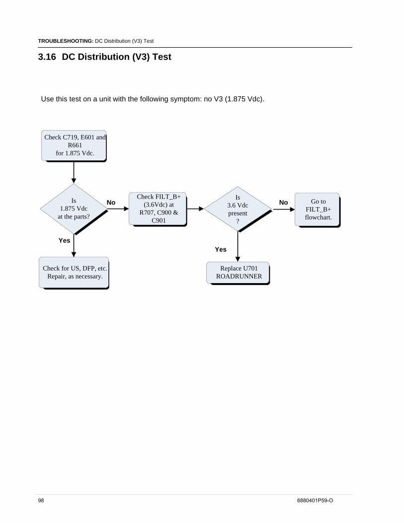
TROUBLESHOOTING: DC Distribution (V3) Test
3.16 DC Distribution (V3) Test
Check C719, E601 and R661
for 1.875 Vdc.
Go to FILT_B+flowchart.
Is1.875 Vdc
at the parts?
Check FILT_B+ (3.6Vdc) at
R707, C900 & C901
Is3.6 Vdcpresent
?
No
YesYes
No
Check for US, DFP, etc.Repair, as necessary.
Replace U701ROADRUNNER
Use this test on a unit with the following symptom: no V3 (1.875 Vdc).
98 6880401P59-O
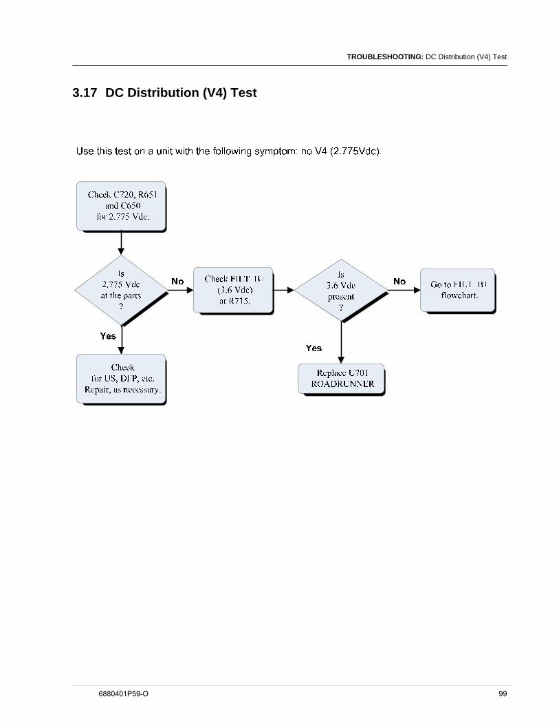
TROUBLESHOOTING: DC Distribution (V4) Test
3.17 DC Distribution (V4) Test
6880401P59-O 99
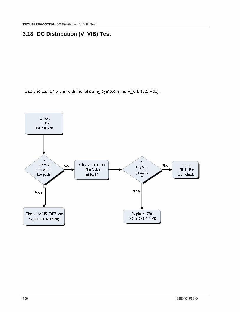
TROUBLESHOOTING: DC Distribution (V_VIB) Test
3.18 DC Distribution (V_VIB) Test
100 6880401P59-O
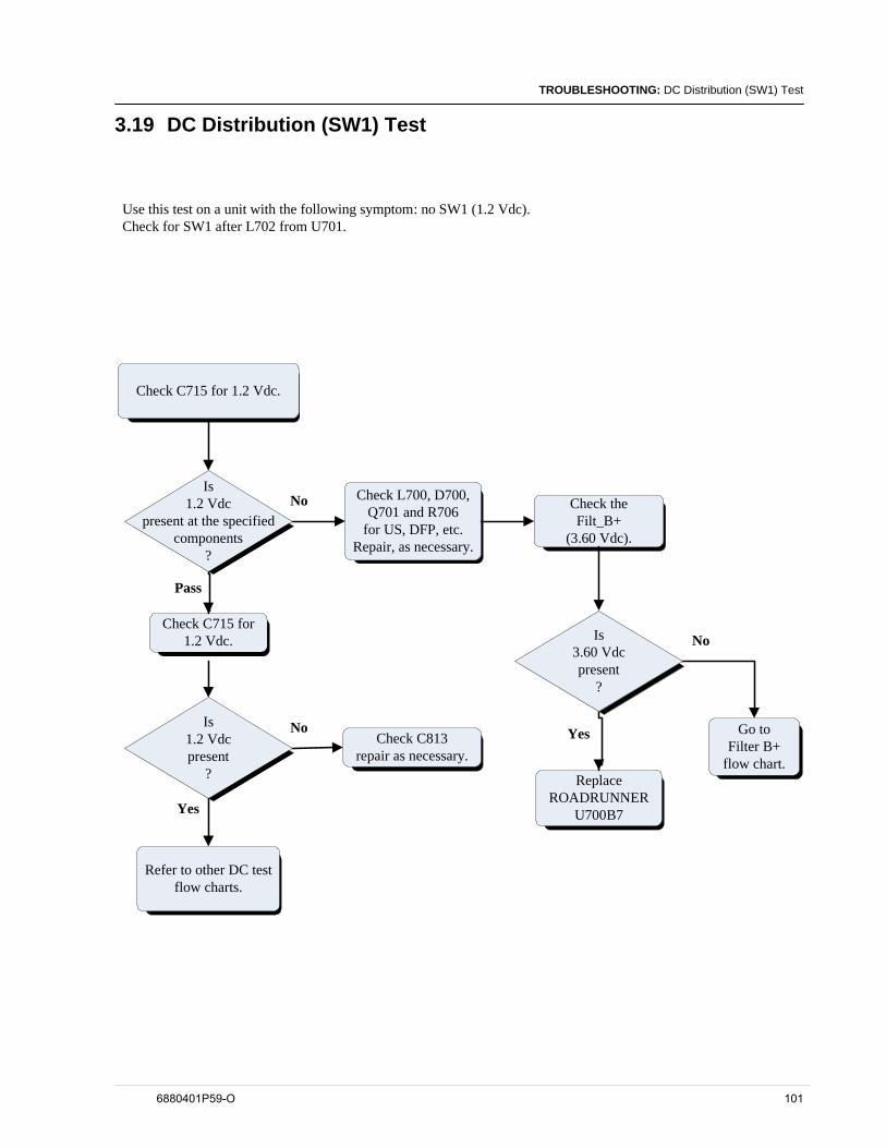
TROUBLESHOOTING: DC Distribution (SW1) Test
3.19 DC Distribution (SW1) Test
Is1.2 Vdcpresent
?
Check L700, D700, Q701 and R706
for US, DFP, etc.Repair, as necessary.
Check C813repair as necessary.
Refer to other DC testflow charts.
Check C715 for1.2 Vdc.
Replace ROADRUNNER
U700B7
Pass
No
Yes
No
Is3.60 Vdcpresent
?
Is1.2 Vdc
present at the specifiedcomponents
?
Go toFilter B+
flow chart.
Check theFilt_B+
(3.60 Vdc).
Yes
No
Check C715 for 1.2 Vdc.
Use this test on a unit with the following symptom: no SW1 (1.2 Vdc). Check for SW1 after L702 from U701.
6880401P59-O 101
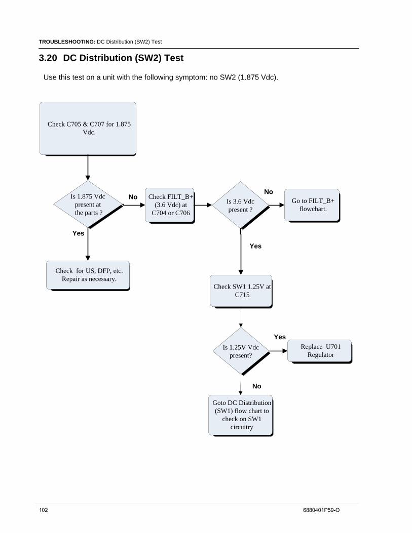
TROUBLESHOOTING: DC Distribution (SW2) Test
3.20 DC Distribution (SW2) Test
Use this test on a unit with the following symptom: no SW2 (1.875 Vdc).
Check C705 & C707 for 1.875 Vdc.
Check FILT_B+(3.6 Vdc) at
C704 or C706
Is 1.875 Vdc present atthe parts ?
No
Yes
Check for US, DFP, etc.Repair as necessary.
Is 3.6 Vdc present ?
Yes
Go to FILT_B+flowchart.
No
Goto DC Distribution (SW1) flow chart to
check on SW1 circuitry
Is 1.25V Vdc present?
Check SW1 1.25V at C715
YesReplace U701
Regulator
No
102 6880401P59-O
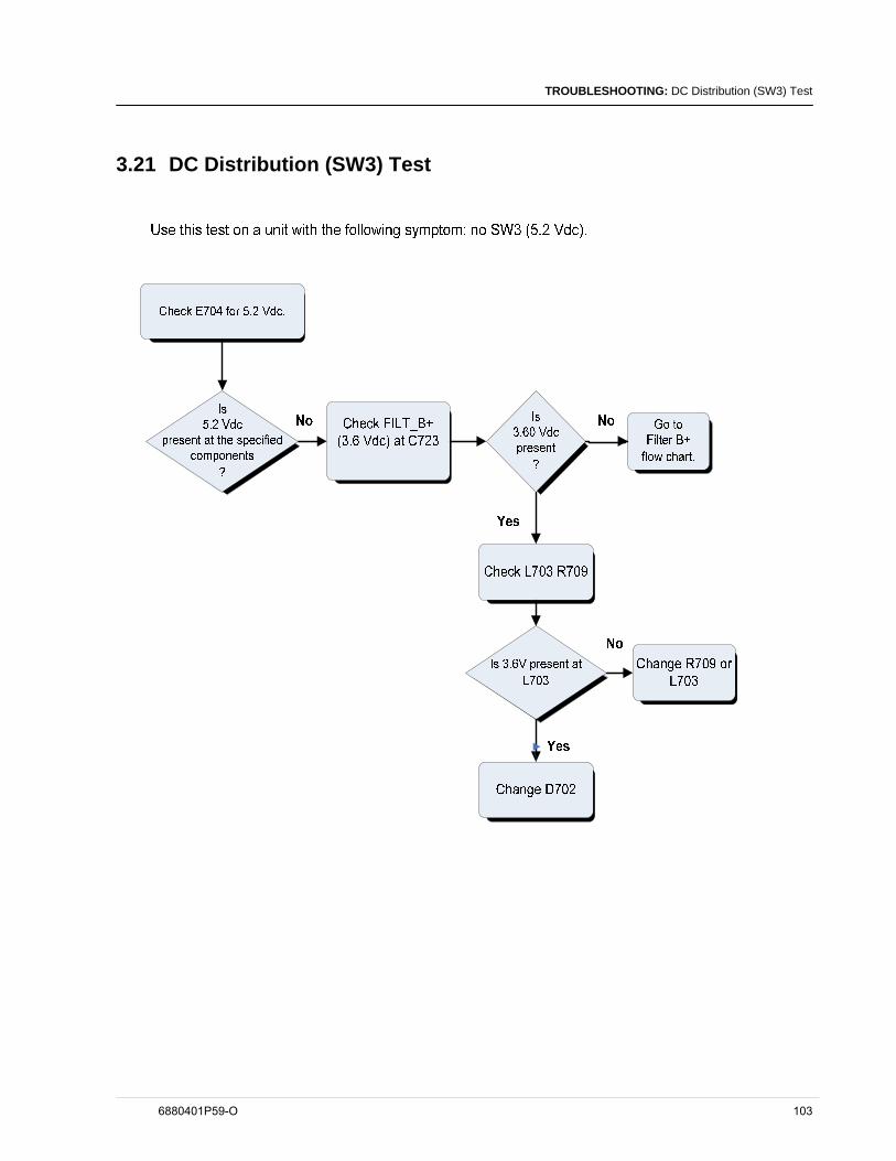
TROUBLESHOOTING: DC Distribution (SW3) Test
3.21 DC Distribution (SW3) Test
6880401P59-O 103
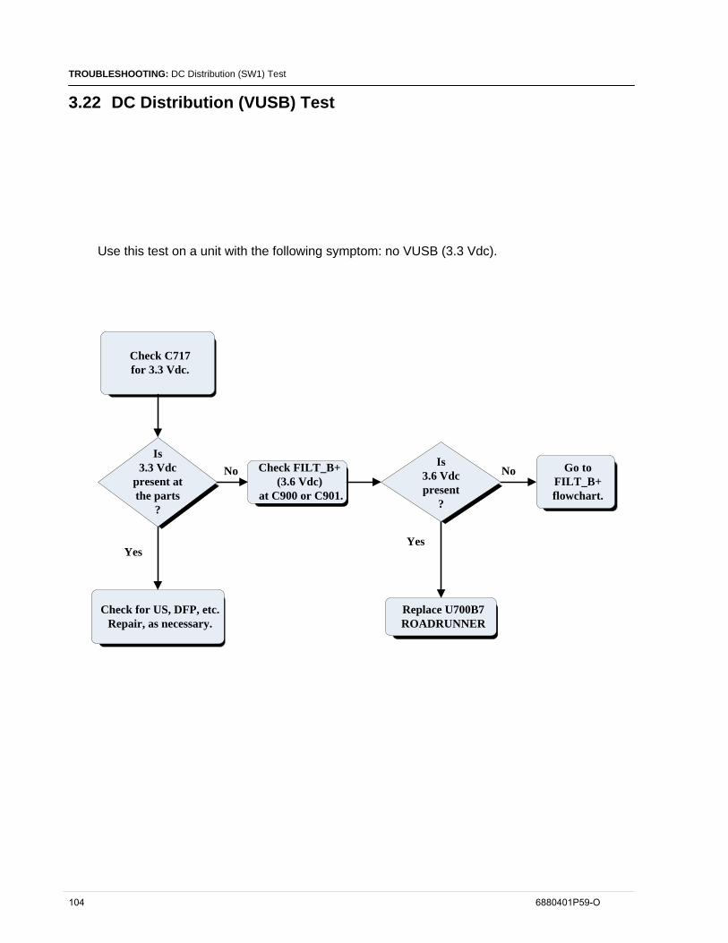
TROUBLESHOOTING: DC Distribution (SW1) Test
3.22 DC Distribution (VUSB) Test
Use this test on a unit with the following symptom: no VUSB (3.3 Vdc).
No
Check C717for 3.3 Vdc.
Check for US, DFP, etc.Repair, as necessary.
Go toFILT_B+flowchart.
Is3.3 Vdc
present atthe parts
?
Yes
Check FILT_B+(3.6 Vdc)
at C900 or C901.
Is3.6 Vdcpresent
?
No
Yes
Replace U700B7ROADRUNNER
104 6880401P59-O
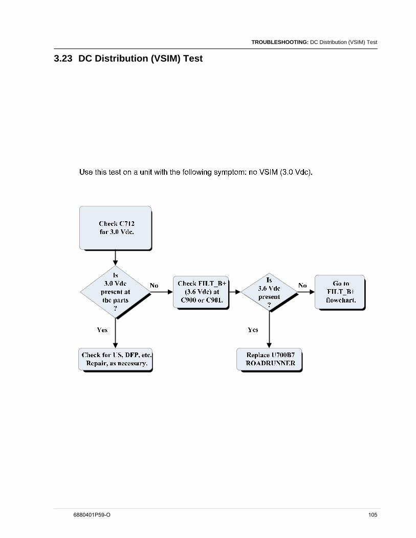
TROUBLESHOOTING: DC Distribution (VSIM) Test
3.23 DC Distribution (VSIM) Test
6880401P59-O 105
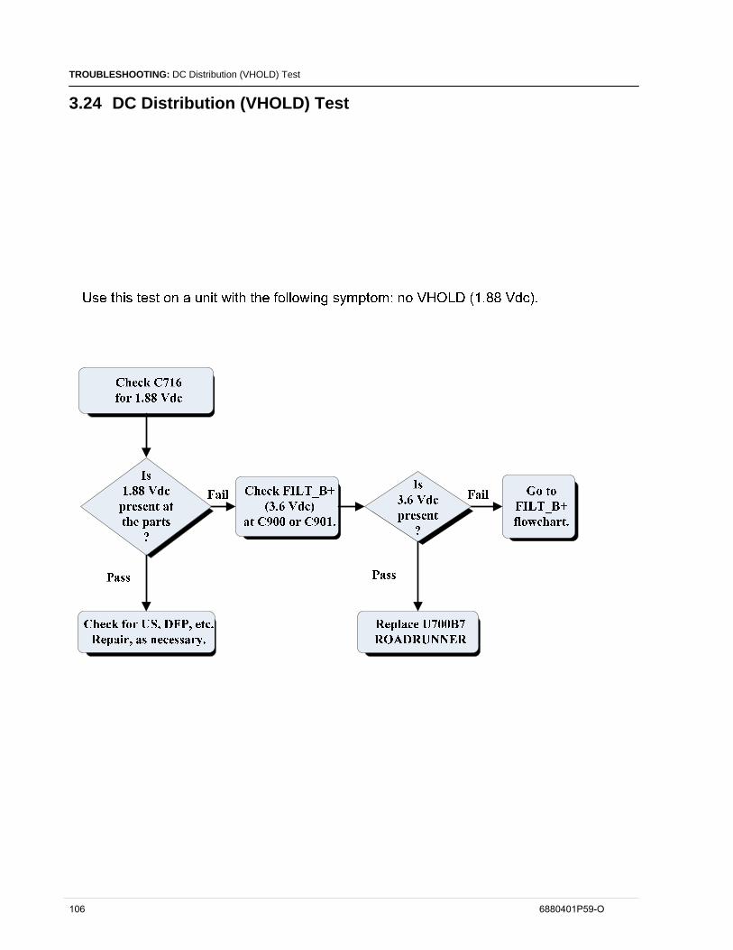
TROUBLESHOOTING: DC Distribution (VHOLD) Test
3.24 DC Distribution (VHOLD) Test
106 6880401P59-O
TROUBLESHOOTING: GPS Receiver Test
3.25 GPS Receiver Test
The Conducted signal testing described below can be performed to analyze or root cause an issue along the GPS RF subsystem, using a CW signal. The following tests are implemented in Factory Test Mode (BERBUG Mode). Test Setup
1. Set up the CW generator as follows: Frequency = 1575.42 MHz, Amplitude level = -80 dBm. Amplitude levels above -76 dBm will compress the Janus IC.
2. Remove the antenna and replace it with a 50 OHM coax. Power up the Unit Under Test (UUT), and connect the CW generator to the UUT.
3. Using Hyper Terminal, GPS is turned on as follows:
BERBUG > gps on
4. Set the Spectrum Analyzer to Center Frequency = 1575.42 MHz, Span = 1 MHz, Amplitude Reference Level = -50 dBm.
5. Use a High Impedance Probe to follow the signal flow along the GPS RF subsystem, block by block.
Block Level Testing of Critical Stages Below is a list of Critical Stages/Blocks, and their respective RF test points:
1. GPS (M500B10): GPS antenna port.
2. Sledgehammer IC (U600B10): IF frequency test pad. DC Power Supply
When testing, it is advisable to utilize an external DC Power supply set at 4 Volts and a current level of 2A. In BERBUG Mode, the UUT is expected to draw 60 mA to 65 mA at power up. By entering “gps on” the UUT should draw 97 mA to 102 mA
6880401P59-O 107
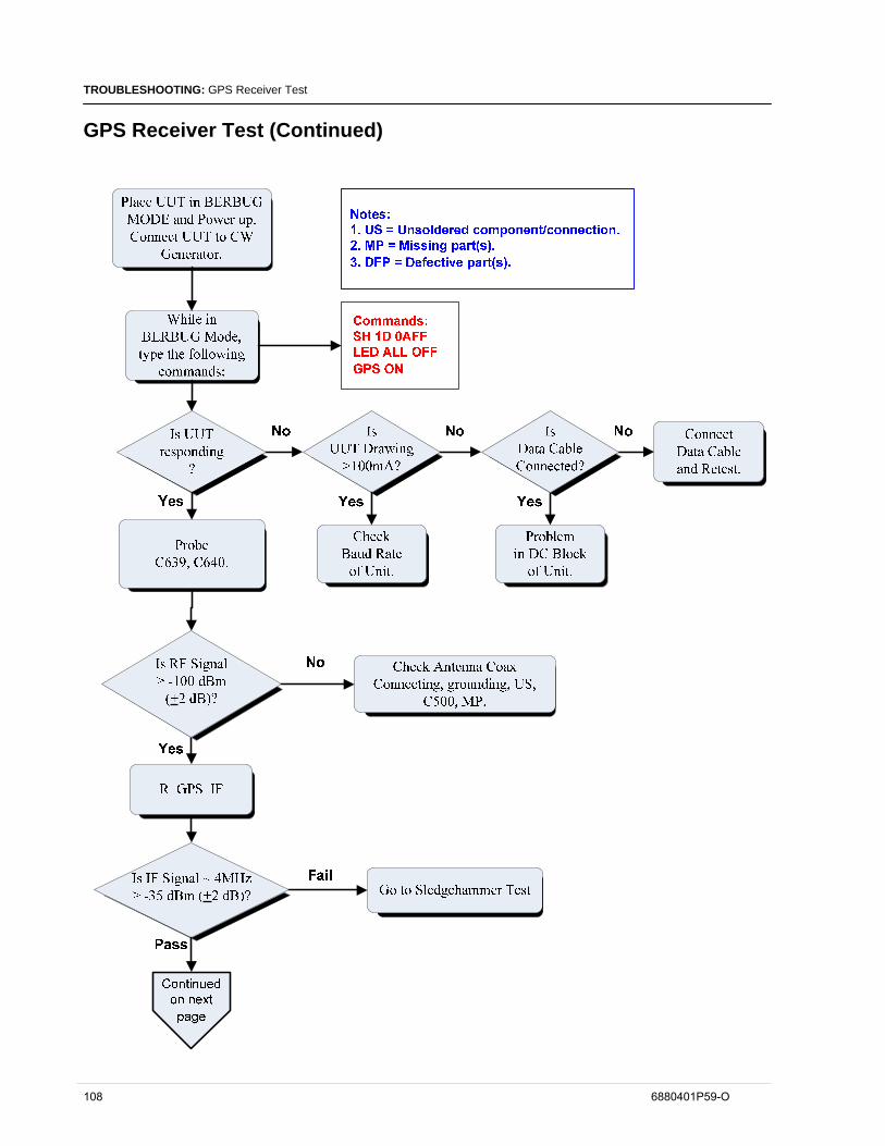
TROUBLESHOOTING: GPS Receiver Test
GPS Receiver Test (Continued)
108 6880401P59-O
TROUBLESHOOTING: GPS Receiver Test
GPS Receiver Test (Continued)
Probe Test Point AN_GPS_CLK
Check L601B10, C678B10
Is clock signal49.107 MHz ≥ -10 dBm?
No
Continued from previous
Page
End GPS testing
Yes
6880401P59-O 109
TROUBLESHOOTING: Digital Analysis Test
3.26 Mototalk
Since the iDEN Receiver and Transmitter Hardware are used for Dispatch (PTT), Phone Call, and MOTOtalk modes of operation; Hardware failures that occur during MOTOtalk will also occur in Dispatch (PTT) and Phone Call modes. Therefore, the electrical troubleshooting guide for MOTOtalk, Dispatch (PTT), and Phone Call are the same.
3.27 Model Assembly (MA) Test Mode Test
• Model Assembly Test Mode is an embedded series of operational tests of the unit's user interface and functional features.
• Motorola iDEN recommends MA Test Mode be performed after any servicing of the unit. • An Audio Test Cable is required to complete test mode correctly. See the Required Tools
section or contact Motorola’s Aftermarket Accessories Division. MA Test mode is achieved by starting from a power-down condition: 1. Press and hold three keys in a row such as 1-2-3, 4-5-6, 7-8-9, ÷-O-#. Simultaneously, press
the Power key 2. Release all keys once the opening screen appears in the main display. 3. Follow instructions as they appear pressing the indicated keys. 4. No instruction? Press any key or Scroll right. 5. No reaction? Power down the unit, check battery condition, and start MA Test again. Screen displays are depicted as follows:
110 6880401P59-O
TROUBLESHOOTING: Model Assembly (MA) Test Mode Test
Model Assembly (MA) Test Mode Test (cont.)
LCD Information Test VPT IST5205 Size 240 x 320
Next Next
The LCD manufacturer and size are displayed on the Main LCD. Press NEXT key
Here we test the LCD display with Color Bars. Press any key to advance
Ellipses are displayed on the main screen for Crosstalk test. Press any key to advance
The gray scale test image is from total black to white indicates that the display has no issues. Press any key to advance
Flicker test screen to check for flicker. Press any key to advance.
Test the LCD with Checkerboard test. Press any key to advance.
Check for camera I2C address, camera device ID, and camera vendor ID. Press any key to advance.
Speak into the internal microphone and listen to the earpiece.
If microphone has been detected, press any key to advance
If microphone not detected, press any key to retest.
Ext LCD TestWintek Size 128x160 Next Mute Key
Check Internal 4 borders
Closed Flip
Viewfinder test screen to verify image. Press YES key to advance.
Then, the camera data lines will be analyzed.
When the data lines test passed, press OK to advance.
The 4 internal borders are one-pixel wide and white. The rest (except text) are black. Close the flip to continue.
CID displays “External LCD test, vendor name and size”. Press mute key to continue.
6880401P59-O 111
TROUBLESHOOTING: Model Assembly (MA) Test Mode Test
Model Assembly (MA) Test Mode Test (cont.)
Color bar pattern is displayed on the modules to capture missing colors. Press any key to continue.
Ellipses are displayed on the main screen for Crosstalk test. Press any key to advance
The gray scale test image is from total black to white indicates that the display has no issues. Press any key to advance
Flicker test screen to check for flicker. Press any key to advance.
Test the LCD with Checkerboard test. Press any key to advance.
External 4 borders
Open Flip
Ext LCD Backlight ON Press any key
Ext key test < 0 > <C CAM C> SEL ViM FLA (+) (-) DEL EXI
CID displays “Open Flip”. And the 4 internal borders are one-pixel wide and white. Open the flip to continue.
Turns on keypad backlight, Main LCD backlight, SOL LED and vibrator. Remove the micro USB seal latch to observe the SOL LED. Verify backlight and vibration
Check for camera I2C address, camera device ID, and camera vendor ID. Press any key to advance.
Ext LED, Ext LED, Backlight On” displayed. Check for the LED functionally. Press any key to continue.
Morphing key turn on. All keys indicators are turned on. As each key is pressed, a short time vibration is felt and the key symbol on the CID disappeared. Continue until the entire keys have been pressed. Once all keys are pressed all key indicator LEDs on touch pad turn off. Proceed with flip open. If test fail, hit the mute key to skip
Vol-Up
Rigth Speaker Tone
Left Speaker Tone
Vol-Down PTT
Right and Left Speaker Tone
PTT
Earpiece Tone
OK
Photosensor: Place radio in light.
Right and Left Speaker tone” displayed and speaker tone was generated. Verifty speaker tone. Press PTT to continue.
“Right Speaker tone” displayed and speaker tone was generated. Verifty speaker tone. Press Volume Up to continue
“Left Speaker tone” displayed and speaker tone was generated. Verifty speaker tone. Press Volume Down to continue.
Verify earpiece audio. Press PTT to continue
Expose photosensor to light and press OK key to advance
112 6880401P59-O
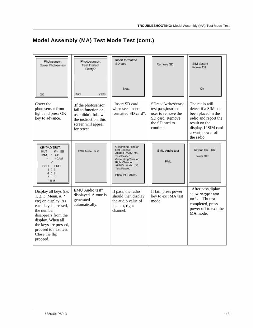
TROUBLESHOOTING: Model Assembly (MA) Test Mode Test
Model Assembly (MA) Test Mode Test (cont.)
Next
Insert formatted SD card
Remove SD
Ok
SIM absent Power Off
Cover the photosensor from light and press OK key to advance.
Insert SD card when see “insert formatted SD card”.
SDread/writes/erase test pass,instruct user to remove the SD card. Remove the SD card to continue.
The radio will detect if a SIM has been placed in the radio and report the result on the display. If SIM card absent, power off the radio
.If the photosensor fail to function or user didn’t follow the instruction, this screen will appear for retest.
EMU Audio test
Generating Tone on Left Channel AUDIO LV=0x1bf5 Test Passed Generating Tone on Right Channel AUDIO LV=0x1b35 Test Passed Press PTT button.
EMU Audio test
FAIL
Keypad test OK Power OFF
After pass,diplay show“Keypad test OK”, Tht test completed, press power off to exit the MA mode.
EMU Audio test” displayed. A tone is generated automatically.
If pass, the radio should then display the audio value of the left, right channel.
If fail, press power key to exit MA test mode.
Display all keys (i.e. 1, 2, 3, Menu, #, *, etc) on display. As each key is pressed, the number disappears from the display. When all the keys are pressed, proceed to next test. Close the flip proceed.
6880401P59-O 113

This Page Left Blank Intentionally
114 6880401P59-O
Schematic Diagrams and COMPONENT LOCATION
Chapter 4 SCHEMATIC DIAGRAMS AND COMPONENT LOCATION When ordering component parts, the part number and reference designator should be included. If the correct numbers cannot be located, call Motorola Parts Identification at 1-847-538-0021.
6880401P59-O 115
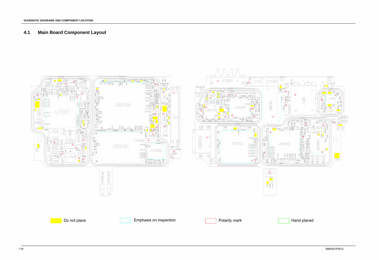
SCHEMATIC DIAGRAMS AND COMPONENT LOCATION
4.1 Main Board Component Layout
116 6880401P59-O
Do not place Emphasis on inspection Polarity mark Hand placed
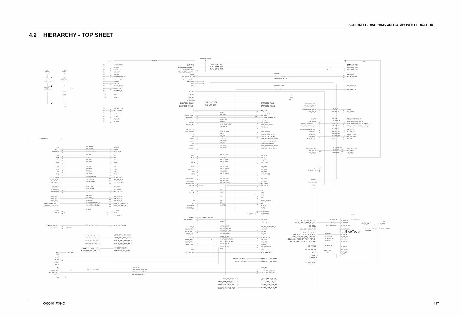
SCHEMATIC DIAGRAMS AND COMPONENT LOCATION
4.2 HIERARCHY - TOP SHEET
6880401P59-O 117
ARDINI Top Sheet, PCB rev10, phone rev Pilot2DELETED GROUNDING CUBESCHANGED BORDER TO D SIZE
Signal not used
ADDED PORTS TO CONNECT STEREO AMP
Thu Apr 15 18:27:22 2010
<CAD_FILE_NAME>
84009289002
84009289002.cpm
1
SH3
1
SH4
1
SH1
4321
SH6
1
SH5
1
SH2
EMU_USB_POWER
V1
SW2_FLTR
LVS
SAP_BITCLK0
FLASH_STROBE
FLIP_RST_B
RR_SEC_INT
ADTRIG
EAR_NEG_TOP
EAR_PLUS_TOP
out
out
EMU_SPI_MISO
inout
EMU_MIC_TOP
in
out
BT_UART_Tx
SAP_FSYNC1
SPI_PRI_CE_SH
HANDSET_MIC_BIAS
EMU_SPKR_TOPEMU_SPKL_TOP
in
in
SAP_RX0
in
Zeus_Shield
out
out
BBP_RX_RXACQ
BBP_GPS_MAG
SPI_PRI_MISO_RR_SH
Janus_Shield
26009267001
26009264001
EMU_Shield
RR_Shield
26009266001
2600926800126009265001
in
out
HANDSET_MIC_BIASHANDSET_MIC_LRC
TCXO_OUT_CLK33_6
GPSIF_ANA_GPS_CLK
GPSIF_IFOUTX
GPSIF_IFOUT
MAIN_VCO_BAND_SEL_2
JANUS_SEL_3
JANUS_SEL_2
JANUS_SEL_1
RXIF_RX_ATTEN
RXIF_AGCDAC
RXIF_RX_STROBE
TXIF_PHCLK
TXIF_TXQ
TXIF_TXI
RXIF_RXQX
PA_TEMP
MAIN_VCO_BAND_SEL_1
TXIF_TXIX
LEFT_SPK_NEG_FILT
LEFT_SPK_POS_FILT
RIGHT_SPK_NEG_FILT
RIGHT_SPK_POS_FILT
STANDBY_OUT_RR
ICHARGE
out
out
out
in
out
in
out
in
in
in
in
in
in
in
out
in
in
in
out
out
out
out
in
out
5
in
in
in
out
in
out
in
out
out
out
out
out
out
in
in
in
in
out
out
out
in
in
in
in
out
in
out
in
in
out
in
in
in
out
out
out
in
out
out
out
in
out
in
out
in
out
in
in
out
in
out
in
in
in
in
out
TAL MOR
TAL MOR
in
in
inout
SH_RESET
out
BT_TCXOout
out
2
out
out
out
out
in
in
in
out
in
in
out
in
in
in
in
in
out
out
out
out
in
in
out
3EMU
in
out
out
out
out
in
in
out
inout
inout
in
out
in
out
out
in
in
in
in
RXIF_RXQ
in
6
inBT_TCXO
STANDBY_OUT_RR
CKIL
in
out
7
ZEUS
inout
out
in
in
out
in
out
inout
inout
out
out
in
out
out
out
out
in
out
in
in
out
out
out
in
in
in
out
out
in
out
out
out
in
in
out
out
out
out
out
out
in
out
in
out
in
in
in
in
in
in
out
in
in
out
in
in
in
out
DSM2
CKO
CKIL
CKIH
EMU_INT
EMU_USB_ID
USB_RXD
USB_TXOE_B
USB_SE0_VM
USB_DAT_VP
EMU_SPI_CS
EMU_SPI_CLK
EMU_SPI_MOSI
HS_USB_DM
HS_USB_DP
USB_HS_SWITCH
USB_ID_PU
BBP_GPS_ACQ_CLK
BBP_GPS_SIGN
SAP_TX
SAP_FSYNC0
SAP_BITCLK1
BBP_TX_TXFS
BBP_TX_TXCLK
BBP_RX_RXFS
BBP_RX_RXCLK
BBP_RX_SRDB
ONE_WIRE
RR_PRI_INT
VSIM_EN
WDI
LV_DETECT
USEROFF
EOLI
SPI_SEC_CE_RR
SPI_SEC_MOSI_RR
SPI_SEC_CLK_RR
SPI_PRI_CLK_RR
SPI_PRI_CE_RR
TOUT2_TXE
TOUT10_JAN_LOAD_SEL
TOUT11_JAN_QUIES_SEL
ONB
SH_RESET
HANDSET_MIC_LRC
SPI_PRI_MOSI_RR_SHBT_PCM_CLK
out
in
SPI_SEC_MISO_RR
out
TXIF_INCR_DECR
BT_RESETB
BT_Shield
BT_PCM_SYNC
BT_PCM_IN
ZEUS_Standby_Out
BT_UART_Rx
out
in
RIGHT_SPK_POS_FILT
RIGHT_SPK_NEG_FILT
LEFT_SPK_POS_FILT
LEFT_SPK_NEG_FILT
out
inBT_PCM_OUT
RR_USBPWR_ADC
EMU_PWRON_RR_ON2
EMU_RESETB
EMU-USBPWR_RR_ON2
TXIF_VTERM
out
out
out
RR_EMU
out
BBP_TX_STDB
out
SAP_RX1
BBP_GPS_AGC_DAT
in
in
out
USER_HARD_RESET
TXIF_TXQX
RXIF_RXI
RXIF_RXIX
out
out
BBP_TX_DMCS
SldgHmr_Shield
out
out
MOBILE DEVICES
PROJECT NAME
BLOCK TITLE:
APPROVALS
LAST MODIFIED BY:
MOTOROLA CONFIDENTIAL RESTRICTEDTHE DRAWING ON THIS PRINT AND INFORMATIONTHEREWITH ARE PROPRIETARY TO MOTOROLA ANDSHALL NOT BE USED OR DISCUSSED IN WHOLEOR IN PART WITHOUT MOTOROLA'S CONSENT.
ENGINEER:
NOT IMPLY PUBLICATIONC
DZONE LTR
COPYRIGHT, MOTOROLA. THIS DOES
D
CAD FILE NAME:
TRANCEIVER
RSTB
PA_ID
PA_TEMP
V_TERM
PHCLK
INCR_DECR
RXI
RXIX
RXQ
RXQX
TXI
TXIX
TXQ
TXQX
MAIN_VCO_BAND_SEL_2
MAIN_VCO_BAND_SEL_1
JANUS_SEL_3
JANUS_SEL_2
JANUS_SEL_1
RX_ATTEN_SL_JN
AGC_DAC_SL_JN
RX_EN_STROB
GPS_IFOUT
GPS_IFOUTX
ANA_GPS_CLK
SPI_DW
SPI_DR
SPI_CLK
CE_SH
TXE
JAN_LOAD_SEL
JAN_QUIES_SEL
VCON
TCXO_OUT_CLK33_6
TCXO_33_6MHZ
GPS_AGC
ASW
RR_EMU
PTT_DET
TSY2
TSY1
PHANTOM_GND
AUX_MIC
A1_INT
HANDSET_MIC_BIAS
HANDSET_MIC_LRC
EMU_MIC
ANT_COLD_SW
SW2_MEM_FB
CID_PWM
KP_LED_PWM
DISP_LED_PWM
CI_BLUE
CI_GREEN
CI_RED
TCXO_OUT_CLK33_6
POWER_FAIL
PHOTO_SENSOR
VPP_OUT
BG_BYP
RR_VDRV4_5_PIN
RR_MOBPORTB_PIN
MUX_OUT
MOD_OUT
VCC_OUT
CS_OUT
VHOLD_EXT_EN
PA_ID
ANA_GPS_CLK
GPS_IFOUTX
GPS_IFOUT
MAIN_VCO_BAND_SEL_2
JANUS_SEL_3
JANUS_SEL_2
JANUS_SEL_1
RX_ATTEN_SL_JN
AGC_DAC_SL_JN
RX_EN_STROB
V_TERM
PHCLK
TXQX
TXQ
TXI
RXQX
RXQ
RXIX
RXI
PA_TEMP
MAIN_VCO_BAND_SEL_1
TXIX
INCR_DECR
LEFT_SPK_NEG_FILT
LEFT_SPK_POS_FILT
RIGHT_SPK_NEG_FILT
RIGHT_SPK_POS_FILT
AUD_PA_EN
EARPIECE_PLUS
FLASH_STROBE
DSM2
TSX1
EMU_USBPWR_RR_ON2
PRIMARY_INT
SECONDARY_INT
STANDBY
EOL_INTERRUPT
EMU_PWRON_RR_ON2
RR_USB_ID
SEC_SPI_CLK
SEC_SPI_MISO
SEC_SPI_MOSI
SEC_CE
USEROFF
BAT_DET_IN
RESETMCU_B
WDI
LV_DETECT
VSIM_EN
BATT_ID_FLTR
ADTRIG
LVS
RR_RAW_EXT_BPLUS_PIN
TSX2
ICHRGE
EMU_AUDIO_LEFT
32KHZ
16.8MHZ
GPS_CLK
GPS_ACQ_CLK
GPS_MAGBIT
GPS_SIGNBIT
DMCS
SDTX
RXFS
SCLK_OUT
RXACQ
SDR
TXCLK
TXFS
TX
RX0
FSYNC0
BITCLK0
BITCLK1
FSYNC1
RX1
PRI_CE
PRI_SPI_MOSI
PRI_SPI_MISO
PRI_SPI_CLK
ON
HAPTICS_EN
EARPIECE_MINUS
EMU_AUDIO_RIGHT
NC
NC NC
NC
NC
NC
NC
NC
NC
NC
NC
NC
NC
NC
NC
NC
NC
NC
NC
NC
NC
NC
NC
NC
NC
NC
NC
NC
NC
NC
NC
EMU
EMU_MIC_RR
EMU_RESET_B
EMU_INT
EMU_USB_ID
USB_ID
ZEUS_4WIRE_USB_SEO_VM_UART2_TX
ZEUS_4WIRE_USB_TXOE_B
ZEUS_4WIRE_USB_RXD
ZEUS_4WIRE_USB_DAT_VP_UART2_RX
EMU_SPI_CS
EMU_SPI_CLK
EMU_SPI_MOSI
EMU_SPI_MISO
USB_HS_SWITCH
HS_USB_DM
HS_USB_DP
EMU_AUDIO_RIGHT
EMU_AUDIO_LEFT
EMU_ICHRG
EMU_POWER_ON
EMU_USB_POWER
RR_USBPWR_AD
BlueTooth
BT_UART_Tx
BT_UART_Rx
NFC_Clk_Rq
BT_VReg_En
BT_Wake
Host_Wake
Main_Clk_RqN
BT_PCM_In
BT_UART_CTS_N
BT_UART_RTS_N
BB_CPU_Clk_RqN
BT_PCM_Out
BT_PCM_Sync
BT_PCM_Clk
BT_Reset_N
BT_V2_7_Pwr_In
TCXO_33_6_MHzBT_Sleep_Clk
ZEUS
USB_HS_DMA_REQ_BT_RTS
USB_HS_WAKEUP_BT_CTS
RIGHT_SPK_POS_FILT
RIGHT_SPK_NEG_FILT
LEFT_SPK_POS_FILT
LEFT_SPK_NEG_FILT
I2DAT
I2CLK
HANDSET_MIC_LRC
HANDSET_MIC_BIAS
BT_RESET
ZEUS_AD3_TXC_BT_PCM_DCLKZEUS_AD3_TXFS_BT_PCM_FSYNC
ZEUS_AD3_RXD_BT_PCM_TXDZEUS_AD3_TXD_BT_PCM_RXD
BP_STBY
ZEUS_UART3_TXD_BT_RXZEUS_UART3_RXD_BT_TX
URST_B
AP_RSTOUT_B
BP_RSTOUT_B
ON_OFF_SWITCH
ZEUS_GROUND
PTT
GPS_AGC_DAT
TOUT11_JAN_QUIES_SEL
TOUT10_JAN_LOAD_SEL
TOUT2_TXE
SPIA_CS6_SH_CE
RR_PRI_SPI_CS
SPIA_MOSI
SPIA_MISO
SPIA_CLK
SPI1_CLK
SPI1_MISO
SPI1_MOSI
SPI1_SS0_RR_SEC_SPI_CS
EOL_INT_B
RR_USER_OFF
USER_HARD_RESET
RSTIN_B
WDI
SIM_SVEN_ZEUS
RR_SEC_INT
TOUT8_RR_PRIMARY_INT
ONE_WIRE
TOUT4_RR_AD_TRIGGER
TOUT0_RX_ACQ
BBP_SRDB
BBP_RXCLK
BBP_RXFS
TOUT1_DMCS
BBP_STDB
BBP_TXCLK
BBP_TXFS
ZEUS_AD2_TXC_RR_DCLK1
ZEUS_AD2_TXFS_RR_FSYNC1
ZEUS_AD2_TXD_RR_RX1
ZEUS_AD1_TXC_RR_DCLK0
ZEUS_AD1_TXFS_RR_FSYNC0
ZEUS_AD1_TXD_RR_RX0
ZEUS_AD1_RXD_RR_TX
GPS_SIGN
GPS_MAG
GPS_CLKACQ
KEYPAD_ROW6_EMU_PU
USB_HS_SWITCH
HS_USB_DP
HS_USB_DM
CSPI2_MISO
CSPI2_MOSI
CSPI2_CLK
CSPI2_SS0_EMU_SPI_CS
USB_DAT_VP_RS232_RX
USB_SE0_VM_RS232_TX
USB_TXOE_B
USB_RXD
MOD_USB_ID
ZEUS_EMU_INT
CKIH
CKIL
CKOH
CKO
FLIP_RST_B
DSM2
FLASH_STROBE
BP_LVS
EARPIECE_MINUS
EARPIECE_PLUS
AUD_AMP_EN
NFC_CLK_REQ_FLT
AUDIO_JACK_LEFT
AUDIO_JACK_RIGHT
AUX_MIC
PHANTOM_GND
PTT_DET
A1_INT
BT_WAKE_B
BT_HOST_WAKE_B
NC
Schematic Diagrams and COMPONENT LOCATION
4.3 ZEUS DIGITAL INTERFACE
118 6880401P59-O
(COMMENT: PIN J801-10 JTAG)
(COMMENT: PIN J801-18 JTAG)
(COMMENT: PIN J801-17 JTAG)
(COMMENT: J801-16 JTAG)(COMMENT: J801-15 JTAG)
COMMENT: CONNECTS TO RR BATT_DET_IN PIN
1IF8
1IF3
1IF9
1IF4
1IF10
1IF1
1IF11
1IF2
1IF5
1IF7
1IF6
1IF12
1IF14
1IF15
1IF16
1IF13
1 TP_BT_RX
1 TP_BT_TX
1 TP_BT_RST
12
6354
M803
R828B6
D828
1CKOHB6
42
1U803B6 6
5
3
U803B6
1TP_TXFSB6
R812B6
21
TP_GPS_S_MB6
1 TP_EOLIB6
1TOUT5B6
R872B6
G1
5678
4321
FL800B6
1
623
4
5
U800B6
3
2
1
U805B6
R820B6
R819B6
R801B6
C804B6
R813B6
1CKILB6
1TP_RXFSB6
1TP_TXCLKB6
1TP_SRDBB6
1TP_STDBB6
C803B6
R811B6
R818B6
R816B6
R803
R814B6
21
C800B6
21 R804 R805B6
B2A2A1
B1
U801B6
1SPIAMISOB6
1SPIAMOSIB6
1SPIACLKB6
1SH_CEB6
1RRPRICSB6
1GPS_TIMEB6
1GPS_ACQB6
21
C802B6
21R808
21
R810B6
21
R809B6
21
R807B6
1 1PPSB6
1 UART2_RXB6
1 UART2_TXB6
AB2
AC1AD1
AC2
C24
L27M22
AE27AD27
M24
K28L23
M26K27
K22J27
J28
H27K23
AB8
AD2
AB7
AA3
AA7
C22
J26F27
G27K26
L26
B23
AE2N12
F28
A24
B25
H19
AF7AG7
C23AG22
B21C13
U804B6
R22R28R27R23
AE3AF2AF3AG3
AG10AC10
AB10AH10
AA10
Y7
P22G23D27
G20
H26P28E26
A13B26P23AG4F26C26F23C27
C7M13
G26D26
K21C25Y8
AA2AF4B20C21AF5
B22H20A23
AH6
AH5
AG6
AG5
AC3
AD3
AG9
AH9
AB9AA9
AF8
AF6
AG8AC7
U804B6
AB22
F22
P27E17G17F19C19H18B19C20
M21N27N26N28C17N22
A20G19
B24
G22
AC6
V21T11U18
B16F15
P12
E27
A16
G15B15M15
R11
H22
Y21AA19
G14
AF27L15A14H14
F14B14
R12
G16C16L17G18
H16B17
B18
F18C18
A19
E28
J24
U804B6
SPI1_CLK
SPI1_SS1_DISPLAY_CS
AP_TSTOUT
IF
IF
IF
JTAG_TRSTBIF
JTAG_TDOIF
JTAG_TDIIF
JTAG_TCKIF
JTAG_SJC_MODIFJTAG_DE_B
IFJTAG_TMSIFBP_TSTOUT
IF
IF
SW2_FLTR
IF
URST_B
UART1_TX
UART1_RX
BP_STBY
IF
IF
IF
ZEUS_UART3_RXD_BT_TX
ZEUS_UART3_TXD_BT_RX
CKOH
UART1_TX
NUF4001MU
SIM_RESET_FSIM_CLK_F
BT_RESET
TEST_POINT
TEST_POINT
AUD_AMP_EN
DISPLAY_SDRR_USER_OFF
FLIP_RST_B
FLASH_STROBEGP_AP_C9_HSUSB_DMA_REQ1
FLIP_OPEN_DET
USB_TXOE_B
USB_RXD
ED_INT4_RAM_DUMP_CTRL
USB_HS_FLAGCUART1_RX
SER_CLK_SEL
UART2_TXUART2_RXLOCK_SW
SPI1_MOSISPI1_MISO
UART1_RX
BT_HOST_WAKE_B
CSPI2_SS0_EMU_SPI_CS
USB_HS_RESET
DSM2
BT_WAKE_B
SER_STBY
ZEUS_AD3_RXC_E_FUSE_REG_CONTROL
USB_HS_SWITCH
USB_HS_WAKEUP_BT_CTSWDI
CAMERA_RESET
BP_STBY BP_STBY
0613952Y17
ZEUS_ONEWIRE_PIN
AP_TSTOUT
USB_HS_INTEOL_INT_B
RR_SEC_INT
USB_HS_DMA_REQ_BT_RTS
FLIP_INT
PTT
AP_TSTOUT SPI1_SS0_RR_SEC_SPI_CS
CSPI2_CLK
RSTIN_B
DISCRETE
ZEUS_AD3_TXD_BT_PCM_RXDZEUS_AD3_RXD_BT_PCM_TXD
ZEUS_AD3_TXFS_BT_PCM_FSYNC
ONE_WIRE
HSUSB_WAKEUP1
ZEUS_AD2_TXC_RR_DCLK1
0613952Y66
SIM_DATA_ZEUS
BP_LVS
URST_B
SIM_RST_ZEUS
ZEUS_UART3_RXD_BT_TX
ZEUS_AD1_TXFS_RR_FSYNC0
CSPI2_MOSI
SW2_FLTR
5175249A04
ZEUS_AD1_TXC_RR_DCLK0ZEUS_AD1_RXD_RR_TXZEUS_AD1_TXD_RR_RX0
SPI1_CLK
ZEUS_AD2_TXD_RR_RX1DISPLAY_ID
ZEUS_AD2_TXFS_RR_FSYNC1
ZEUS_AD3_TXC_BT_PCM_DCLK
ZEUS_AD3_RXFS_NFC_GPIO2
PC29973VXDR2
URST_B
CKO
CKIH
ZEUS_EMU_INT
CSPI2_MISO
RSTIN_B
AP_RSTOUT_B
CKIH
47K
BP_RSTOUT_B
E_FUSE_REGULATOR_CONTROL
0613952Y66
3971599M02
4.7K
SIM_DATA_F
VSIM
SW2_FLTRV2
0
SPI1_SS1_DISPLAY_CSUART1_TX
SPI1_MOSISPI1_MISO
ZEUS_UART3_TXD_BT_RX
CAMERA_PD
0
HARD_RST_R_C
0613952P68
E_FUSE_REGULATOR_CONTROL
EF_PGM
0
DISCRETEDISCRETE
MOD_USB_NEG_IN
100K VREG_FILTER
SW2_FLTR
MOD_USB_ID_GATEDTXS03121
BMOD0
FLASH_ENVM
TOUT2_TXE
0
1SS390
LP5900
VREG_FILTER_R_C
499K
ON_OFF_SWITCH
2113956A51
NLU1GT32
BBP_STDB
RR_PRI_SPI_CSSPIA_CS6_SH_CE
SPIA_MOSISPIA_MISO
SW3
0
.1UF
100K
0
V1_FLTR
SPARK_GAP
SW3
.22
100K
VSIM_FILT
MAX803
GPS_CLKACQ
BBP_SRDBBBP_TXCLK
EF_PGM
SPIA_CLK
1UF
100K
FILT_BPLUS
SW2_FLTR
.1UF
DISCRETE
0613952Y25
3.3UF
BP_TSTOUT
NLU1GT32
BMOD2
5175858M01
BP_TSTOUT
TOUT11_JAN_QUIES_SEL
TOUT6_GPS_1PPSZEUS_TOUT5
TOUT2_TXETOUT1_DMCS
GPS_AGC_DATGPS_MAGGPS_SIGN
BBP_RXFSBBP_RXCLK
TOUT10_JAN_LOAD_SEL
GPS_TIMEMARK
BBP_TXFS
PC29973VXDR2
5175249A04
USB_SE0_VM_RS232_TXUSB_DAT_VP_RS232_RX
CKIL
SIM_SVEN_ZEUS
PC29973VXDR2
5175249A04
TOUT0_RX_ACQ
TOUT8_RR_PRIMARY_INT
IPU_SPI_MISO
ON_OFF_SWITCH
0
BMOD1
MOD_USB_ID
SIM_CLK_ZEUS
100K
TOUT4_RR_AD_TRIGGER
USER_HARD_RESET
100K 100K
OUT
OUTOUT
OUT
OUT
OUTOUT
IN
IN
OUT
INOUTOUT
BI
OUT
OUT
IN
OUT
OUT
OUT
OUT
OUT
IN
OUTIN
IN
OUT
SIM_DATANC
GND
SIM_CLOCKSIM_RESETVSIM
IN
OUT
OUT
OUT
NC
OUT
NCNC
GND
VCC
OUT
OUT
OUT
NCNC
NC
NC
NC
OUT
NC
NC
NC
NC
NC
NC
NCIO
NC
NC
IN
NC
ININ
FLTR4FLTR3
FLTR1FLTR2FLTR3FLTR4
GND1
FLTR1FLTR2
IN
OUT
OUT
OUTOUT
OUTOUT
IN
CSPI2
CRM_COM
SHARED
DOMAIN
USB
OTG
USB
HOST2
USB
HOST1
UART3
CEBusSIGNALS
SIM
BLOCK
SPI2_CLK
SIM_PD
SPI2_SS1
SIM_RST_BSIM_SVEN
SIM_TRXDSIM_CLK
UH1_RXDMUH1_OVRUH1_PWR
SPI2_MOSISPI2_MISOSPI2_SS0
STBYLVS
CKILBP_RSTOUT_B
RSTIN_BURST_BAP_RSTOUT_B
CKIHCKOCKOH
USB_TXOE_BUSB_DAT_VPUSB_SE0_VM
USB_RXD
U3CE_CTS_BU3CE_DSR_BU3CE_RI_BU3CE_DCD_BU3CE_DTR_B
UH2_DPUH2_DMUH2_OVRUH2_PWR
UH1_TXOE_BUH1_SPEED
UH1_SUSPENDUH1_TXDPUH1_TXDMUH1_RXDUH1_RXDP
OUTOUTOUT
OUTOUT
OUT
OUTOUT
OUT
OUT
IN
OUT
OUT
IN
OUT
IN
V_POS
POS_INNEG_IN
SD
GND
VCC
GND
RESET
NC
OUT
IN
IN
IN
GPT
DOMAIN
SIGNALS
BLOCK
GPIO
GENERALUART1
CSPI1
AUDIO1
SIGNALS
AP
UART2
ONE WIRE
AUDIO3
AUDIO2
SPI1_MOSI
AD1_TXFS
SPI1_MISOGP_AP_C0GP_AP_C1
ED_INT0ED_INT1ED_INT2ED_INT3ED_INT4
GP_AP_C2
AD2_RXDAD2_TXCAD2_TXFS
GP_AP_C3GP_AP_C4GP_AP_C5GP_AP_C6GP_AP_C7
ED_INT5ED_INT6ED_INT7
GP_AP_C8GP_AP_C9GP_AP_C10GP_AP_C11
U1_TXDU1_RXD
U1_RTS_BU1_CTS_B
U2_TXDU2_RXD
U2_RTS_BU2_CTS_B
SPI1_CLK
SPI1_SS0SPI1_SS1
AD1_TXDAD1_RXDAD1_TXC
AD2_TXD
AD3_TXDAD3_RXDAD3_TXCAD3_RXCAD3_TXFSAD3_RXFS
OWDAT
BMOD0BMOD1BMOD2MUX_CTRL
ICAP1ICAP2ICK_APOC1OC2OC3
IN
OUTBI
IN
VOUT
GND
VINVEN
IN
IN
OUT
IN
IN
OUTOUT
IN
IN
ININ
IN
ININ
ININ
IN
MISC
L1T
MQSPI
GPS
DIGiRF
BP
DOMAIN
SIGNALS
BLOCK
JTAG
BBP
BPSPI1_MOSIBPSPI1_CLK
DIGIRF_TXDDIGIRF_TXEDIGRF_SYSCLKEN
ACQCLK
DIGRF_CDATDIGRF_CEN
SC2B
DIGRF_SCLK
TIMEMARK
BPSPI_CS2
BPSPI2_MISOBPSPI2_MOSIBPSPI2_CLK
BPSPI_CS1BPSPI_CS0 TRST_B
TDOTDITCK
RTCKTMSDE_B
SJC_MOD
BPSPI1_MISO
TOUT10
TOUT8
STDBSRDBSCKBSC0BSC1B
DIGRF_CCLK
SIGNMAGAGCDAT
EFUSE_PGM
VREG_FILTERTEST
TOUT0TOUT1TOUT2TOUT3TOUT4TOUT5TOUT6TOUT7
TOUT9
EFUSE_GND
TOUT11TOUT12TOUT13TOUT14TOUT15
BPSPI_CS3
SCHEMATIC DIAGRAMS AND COMPONENT LOCATION
4.4 ZEUS MEMORY INTERFACE
6880401P59-O 119
PLACE BY PIN H2
PLACE BY PIN P6PLACE BY PIN C8 AND C4
PLACE BY PIN P4 AND P8
R853B6
C867B6
R852B6
1DDR_DATA_8B6
1 DDR_UDQSB6
C897B6 C863B6
C865B6C864B6C861B6 C858B6
C856B6 C859B6C857B6
C860B6
R850B6
1DDR_DATA_0B6
1
WEMI_D_3B6
N3
P9P7P5H10G2C9C5
P8P4H2 P6C8C4
L7E3
F6
B3B2
T12
B1
T11H11T10
T3T2T1
R12R11R10R3
A12
R2R1P12
P11P3P2P1N2M2L2
A11
K10K9K8K5K4K2J11
J10J9J8
A10
J7J6J5J4J3J2H9H8H7H6
A3 H5H4H3G10
G9G6F9F2E2D3A2 D2D1C12
C11
C3C2C1B12
B11
B10
A1
L6
N11C10D10E10F10L10M10N10P10
D11E11F11G11K11L11M11
M3
D6
K7
F3
K6
K3
D7
G3
L3
N7M7N6M6N5M5L5N4
N9M9L9N8M8L8
M4L4
D5
C6C7
E6
F5E5
G7D9D8E8F8G8G4F4
E9E7F7G5
E4D4
U806B6
1 DDR_WEB6
1 DDR_RASB6
1 DDR_CASB6
1 DDR_CSBB6
1
NAND_CLEB6
1
NAND_ALEB6
1
NAND_CEB6
1
NAND_REB6
1
NAND_WEB6
1
NAND_WPB6
R851B6
R844B6R846B6
C866B6
1 DDR_LDQSB6
21
C862B6
1
DDR_A0B6
R845B6
C855B6
R843B6
C12H12
V8
W2
U2V2
W1Y1
T1V7
N3N7N2M5M3L6L3L7
T3T2R2R6P2P6
K3K6
G10
B12
V6
A5
Y3
B6H9 R1
N1
U7P1
A9F10B10G11A10C10B11F11
B7C8B8C9B9
H10
C11L12
U3
F7G7F6C5G8B5
L13
G13
V3
H11
G9G6
A6
B13
H3 H2 H7 J1 J2 J7 K1 K2B4 C4 B3 C6 C3 E3 L2C2 D3 F3 D2 E1 E2 G3 F1 F2 G2 M2
U804B6
SDRAM_CLKSDRAM_CLKB
SDRAM_CLK_ENSDRAM_CAS
NAND_REBNAND_WEBNAND_WPBNAND_READY
NAND_ALENAND_CLE
SDRAM_CSB
00613952Y66
2113945F07
.01UF2113945F07
DDR_VDD
0613952Y66
.01UF
2113945F07
DDR_VDD
MEM_VREF 0613952W
01
SW2_FLTR
PC29973VXDR2
0613952Y01
10K
NAND_CEB
NAND_VCC
SDRAM_ADD(13:0)
2113946U01 2175511A01
2.2UF
SDRAM_WEB
SDRAM_CLK_EN1
DDR_VDD_1
.1UF .01UF
NAND_VCC
2113945F07
2187893N01
.1UF2113946U01
100K
NAND_WPB
15
SDRAM_LDQS
.1UF
SDRAM_UDQMSDRAM_BA0
0613952W
01
10
7
14
H8BCS0SI0MAP
6
1110
2113946U011UF
NAND_REBNAND_CEB
1UF
SDCLK_B
2187893N01
2113945F07.1UF.01UF
0
SDRAM_CSBSDRAM_WEBSDRAM_RAS
SDRAM_LDQM
SDRAM_BA1
543
0
13
10
6
11
2
14
HS_USB_ADDR17
HS_USB_ADDR16
HS_USB_ADDR15
CS5_B
RW_B
WEMI_DATA(15:0)
SDRAM_DATA(15:0)
10WEMI_DATA(15:0)
NAND_READYSDRAM_UDQS
NAND_CLENAND_ALE
NAND_WEB
10
1312
789
6
1
131415
12
543
10
2
13
1112
98
6543
11
0
11
21
3
76
109
1415
13
3
9
12
12
4
8
8
OE_B
5
7
12
8
5
4
.01UF
210
2187893N011UF
SDRAM_DATA(15:0)
2
SDCLK
13
15
0
2113946U01
7654
2
SDRAM_LDQMSDRAM_CAS
100K
9
789
SDRAM_ADD(13:0)
10
SDRAM_CLKBSDRAM_CLK
1
11
SDRAM_UDQM
SDRAM_RAS
3
SW2_FLTR
0
.1UF
5175249A04
SDRAM_UDQSSDRAM_LDQS
SDRAM_BA0SDRAM_BA1
010
SW2_FLTR
NAND_VCC
0613952Y66
2113946U01
NC
NC
NC
NC
NC
NC
NC
NC
NC
NCNC
NC
NCNC NC NC NC NC NC NC NCNC NC NC NCNC NC NC NCNC NC NC NCNC NC NC NCNCNCNCNC
NC
NCNC
NC
NC
NC
NCNC
NC
NC
NC
NC NC NC NC NCNCNC NC NC NCNC NC NCNCNC NC NC NC NC NCNC NCNC NC NC NCNCNCNCNC
NC
RY_BY*
EN_CK
NC17
A0
EN_WE_D
NC69
NC42
RASCAS
CLKCLK*
BA0BA1
EN_LDQMEN_UDQM
A8
A13
DQ6
DQ3
DQ1DQ2
IO11_NAND
A5
DQ5
IO3_NAND
UDQS
VCC_N
A1A2
LDQS
IO15_NANDIO16_NAND
NC2
IO2_NAND
IO4_NANDIO5_NANDIO6_NANDIO7_NANDIO8_NAND
NC14
NC15_DNU
NC16
NC18
DQ0
DQ4
DQ7DQ8DQ9
DQ11
DQ13DQ14DQ15
NC1
NC3
NC4
NC5
NC6
NC7
NC8
NC9
NC10
VSS7
A3A4
A7
A9A10A11A12
VSS6
VSS1
VSS2
VSS3
VSS4
VSS5
VCC_D1
VCC_D2
VCC_D3
VCCQ_D1
VCCQ_D2
IO14_NANDIO13_NANDIO12_NAND
IO10_NANDIO9_NAND
DQ10
DQ12
IO1_NAND
CS
A6
NC21
NC20
NC19
WP_NAND
NC11
NC12
NC13
NC22
NC23
NC24
NC25
NC26
NC27
NC28
NC29
NC30
NC31
NC32
NC33
NC34
NC35
NC36
NC37
NC38
NC39
NC40
NC41
NC43
NC44
NC45
NC46
NC47
NC48
NC49
NC50
NC51
NC52
NC53
NC54
NC55
NC56
NC57
NC58
NC59
NC60NC61NC62NC63NC64NC65NC66
NC67NC68
NC70
EN_WE_NAND
EN_CE_NANDEN_RE_NAND
EN_CLE_NANDEN_ALE_NAND
NCNCNCNCNCNCNCNC
SDRAM
DATA
CONTROL
DATA
NAND
WEMI
INTERFACE
MEMORY
CONTROL
ADDRESS
A4_MA4
A3_MA3
A2_MA2
A1_MA1
SDCLKSDCLK_B
A15
A16
BE1_BOE_B
BCLK
D0
ECB_WAIT_B
SDWE_B
CS4_BCS5_BBE0_B
RW_BLBA_B
D1D2D3D4D5D6D7D8D9D10D11D12D13D14D15
CLEALECE_B
WP_BBSY_B
A23
A22
A21
A20
A19
A18
A17
A14
A13_MA13
A12_MA12
A11_MA11
A10
A9_MA9
A8_MA8
A7_MA7
A6_MA6
A5_MA5
A0_MA0
MA10
VREF
CS0_BCS1_B_A26
CSD0_BSDBA0
CS2_BCS3_B_CSD1_B
SDBA1DQS0DQS1
SDCKE0SDCKE1
RAS_BCAS_BDQM0DQM1
SD0SD1SD2SD3SD4SD5SD6SD7SD8SD9
SD10SD11SD12SD13SD14SD15
RE_BWE_B
A25
A24
SCHEMATIC DIAGRAMS AND COMPONENT LOCATION
4.5 ZEUS POWER
120 6880401P59-O
Legacy locationPlaced before 0 ohms
CURRENT SENSE AND DECOUPLING CAPACITORS
1.875V
1.875V
2.775 V
1.8 V
2.775 V
1.875V
2.775 V
1.875 V
1.875V
3.0 V
C882B6
R874B6
R878B6
C888B6
C890B6
C892B6
C893B6
C884B6
C886B6
C885B6
C887B6
C889B6
C891B6
C833B6
C829B6
C825B6
C834B6
C831B6
C830B6C812B6 C813B6
R833B6
AH23
AE26
AF22E9B28
B27
AG27
AG28
AH27
AD20
AD17
B2AD12
AC14
AB18
AB11AB6
AA18
AA15
AA12
AA11Y24
AH28
Y5W21W7
W6
W3
V13
U24
U17
U16
U15
A28
U14
U13
U12
U11U5T17
T12T7R17R8
A27
P17
P11P7N21
N18
N17
M17
M14
M12
M11
A2
M7L22L8K8J22J5J3H17
H15
E20
A1
AC26
AA22
M27
L21
M16
AG23
AC22
L16
G21
M18
AF9
P18
AC15
AF12
T18
T21
R21
T28
AB3
V15
U8T8R7P8N11
K7J8H13
E12
AF26
A15
AC19
AC18
AB20
V16
V12
R18
P21
N8M8L14
J21
AF11
AD9
AB19
W8
G12
AG21
Y2
AG2AG1AH2AH1B1
U804B6
21
C853B6
21
C854B6
21
C852B6
21
C846B6
21
C851B6
21
C845B6
21
C850B6
21
C843B6
21
C848B6
21
C844B6
21
C849B6
21
C837B6
21
C841B6
21
C838B6
21
C842B6
21
C836B6
21
C835B6
21
C839B6
21
C817B6
21
C816B6
21
C815B6 2
1C820B6
21
C824B6
21
C826B6
C823B6
21
C819B62
1C814B6
21
C811B6
21
C810B6
21
C809B6
??
$NET_PHYSICAL_TYPE=?
$NET_PHYSICAL_TYPE=?
??$NET_PHYSICAL_TYPE=?
$NET_PHYSICAL_TYPE=?
$NET_PHYSICAL_TYPE=?
$NET_PHYSICAL_TYPE=?
$NET_PHYSICAL_TYPE=?
?$NET_PHYSICAL_TYPE=?
$NET_PHYSICAL_TYPE=?
$NET_PHYSICAL_TYPE=?
$NET_PHYSICAL_TYPE=?
$NET_PHYSICAL_TYPE=?
$NET_PHYSICAL_TYPE=?
$NET_PHYSICAL_TYPE=?
?
82PF
Z_VDD_CORE
2113946U01
2113946U01
2113946U01
.1UF
82PF
.1UF
$NET_PHYSICAL_TYPE=?
2113946U01
2113946U01
2113946U01
SW1_FB SW1
.1UF
2113946U01
2113946U01
.1UF
2113946U01
2113946U01
2187893N01
.1UF
2113946U01
.1UF
VSIM
2113946U01
2113946U01
Z_VDD_SD1
2113946U01
.1UF
Z_VDD_UH2
SW2_FLTR
2113946U01
.1UF
Z_VDD_UH2
SW2_FLTR
SW2_FLTR
2113946U01
2113946U01
SW2_FLTR
2113946U01
.1UF
2113946U01
.1UF
.1UF
.1UF
SW2_FLTR
2113946U01
.1UF
SW2_FLTR
SW2_FLTR
.1UF
.1UF
.1UF
.1UF
2113946U01
2113946U01
.1UF
.1UF
2113946U01
.1UF
.1UF
.1UF
.1UF
.1UF
2113946U01
.1UF2113946U01
.1UF2113946U01
.1UF
SW2
Z_VDD_KPP
V1
RR_VUSB
ZEUS_GROUND
2113946U01
SW2_FLTR
.1UF
.1UF 2113946U01
.1UF
.1UF
.1UF
SW2_FLTR
2113946U01
2113946U01
1UF
.1UF
0
2113946U01
2113946U01
0
SW2_FLTR
2113946U01
SW2_FLTR
V1_FLTR
1UF
.1UF
SW2_FLTR
2113946U01
.1UF
.1UF
2113946U01
2113946U01
2113946U01
.1UF
SW2_FLTR
SW2_FLTR
SW2_FLTR
.1UF
Z_VDD_SD1
SW2_FLTR
SW2_FLTR
SW2_FLTR
VSIM
SW2_FLTR
SW2_FLTR
SW2_FLTR
SW2_FLTR
Z_VDD_CORE
.1UF
.1UF 2187893N01
2113946U01
2113946U01
.1UF
.1UF
2113946U01
2113946U01
.1UF
2113946U01
2113946U01
V1_FLTR
.1UF
.1UF
SW2_FLTR
SW2_FLTR
PC29973VXDR2
Z_VDD_KPP
Z_VDD_SD1
0
VMMC
SW2_FLTR
OUT
VDD_RRSH4_2
VDD_CSI_3
VDD_IPU2
VDD_UH1
NC1
VDD_CSI_2
VDD_CKIH
VDD_FUSEBOX
VSS_FUSEBOX
VSS_CKIH
VSS_DSCLK
VDD_EMI_2
VDD_CORE13
VDD_CORE11
VDD_CORE8
VDD_CORE7
VDD_CORE1
VDD_CORE2
VDD_CORE3
VDD_CORE4
VDD_CORE6
VSS61
VSS13
VDD_SD1
VDD_SD2
VSS12
VSS11
VSS10
VDD_RRSH2
VDD_SIM
VDD_IPU1
VDD_GEN1
VDD_GEN2
VDD_RRSH3
VDD_DSCLK
VDD_STBY
VDD_VREGPW
R
VDD_RRSH1
VSS2VSS1
VSS63
VSS64
VSS59
VDD_KPP1
VSS29
VSS31
VSS32
VSS33
VSS34
VSS36
VSS37
VSS38
VDD_EMI_1
VSS30
VSS9
VSS14
VSS4
VSS7VSS6
VSS16
VDD_CSI_1
VSS15
VSS50
VSS51
VSS53
VSS40
VSS45
VSS47
VSS60
VDD_CORE10
VDD_CORE5
VSS54
VSS55
VSS56
VSS57
VDD_DIGRF
VDD_KPP2
VDD_RRSH4_1
VDD_UH2
VDD_CE
VSS5
VSS3
VSS28
VSS23
VSS8
VSS58
VSS52
VSS62
VDD_JTAG
VSS18
VSS19
VSS20
VSS21
VSS22
VSS24
VSS25
VSS26
VSS27
VDD_EMI_3
VDD_EMI_4
VDD_EMI_5
VDD_EMI_6
VDD_EMI_7
VDD_EMI_8
VDD_EMI_9
VSS17
VSS39
VSS41
VDD_CORE9
VDD_CORE12
VSS35
VSS42
VSS43
VSS44
VSS46
VSS48
VSS49
NC2NC3
NC5NC4
SCHEMATIC DIAGRAMS AND COMPONENT LOCATION
4.6 DISPLAY AND CAMERA INTERFACE
6880401P59-O 121
(MPN 5170200D37)
R821 DNP for Brightwater
R888 DNP for Brightwater
Place FIN668
R822 DNP for Muscardini
SMART SPI SMART PAR
DUMB
NOTE: KEYPAD ROW 7 IS USED
R889 DNP for Muscardini
R890
R889
R822
R821
21
VR852B6C871B6
1IPU_OEB6
1IPU_VSYNCB6
1IPU_HSYNCB6
R888B6
8765
4321
G2 G1
910
J802B6
C794B6
C790B6 C793B6C792B6C791B6
B1B2A2
A1
U790B6
21
VR801B6
E887B6
C821B6 C827B6
C832B6C828B6
E888B6
R877B6R876B6
C874B6
E2 C2F2
E3
B4A4
A2
B2
A1
F3
D3
D2 C1
G1F1
D5E6E5
F6
G6F5G5E4
A5A6B5B6C5C6D4D6
G4F4
B3A3C3C4
B1
D1E1
G3
G2
U807B6
L800B6
G1
910111213141516
87654321
FL803B6
5
3 2 1
4
Q801B6
R856B6
AA20
AF25AG25AG24AH24
V17AG26
AA14
AF24AF21AF20AF23
V14AA17
AH13
AF13
AG13
AB13
AG12
AB12
AG11
AF10
AH16
AG15
AA16
AH15
AH14
AB15
AG14
AB14
AB23AA26
W26
AB26
W28U26V27U22V26U21U27T22
AD26AC28Y27W22Y28V23W27V22
T27T26
AC23
AB27
AD28
AC27
Y26
W23
AA27
Y22AB16AG16
AC11AG20AH20
AA13
AF19AB21AF18AH19AF17AG19AF16AG18AB17AG17
U804B6
C870B6
E806B6
IPU_SPI_CLK
DISP_CLK
ONE_WIRE82PF82PF
SD_CARD_DET
CSI_MCLK_MSEO1_B_FLTR10
4.7PF
6.8NH
CSI_MCLK_MSEO1_BCSI_PIXCLK_FILT
SD1_DATA1SD1_DATA0
14
SD1_DATA3_Z
13
82PF
82PF
SERDES_VDDS
EXT_DISP_EN
VMMC
SD1_CLK_L
SD1_DATA3SD1_DATA2
SD1_CMD SD1_CMD_Z
EXT_DISP_REG_SEL
CKS_P
IPU_SPI_CSEXT_DISP_ENMAIN_DISP_ENIPU_D3_VSYNCIPU_D3_HSYNC
.1UF
SERDES_VDDA
SW2_FLTR
5109817F88
0
17
10
7
PC29973VXDR2
CSI_D5_MDO5
CSI_D7_MDO7CSI_D8_MCKO
CSI_VSYNCCSI_HSYNC
CSI_D1_MDO1CSI_D2_MDO2
CSI_D4_MDO4
CSI_D9_MSEO0_B
1516
KEYPAD_ROW6_EMU_PU
0
.1UF
V1_FLTR
1
34
6
89
1112
2
KEYPAD_ROW6
100KKP_ROW6_SW
65 7
4 5210
20
4885316E03
4
V1_FLTR
KP_COL(7:0)
CSI_HSYNCCSI_VSYNC
SW2_FLTR1K1K
3
0
3
7
56NH
4.7UF
VMMC
1
SD1_DATA0_Z
EMC5
7.6VCDZ7-5B
7.6V
LP5990
CDZ7-5B8.2PF
4.7UF
NUF8001MU
SD1_DATA1_Z
1
8
5
33PF
9
6
DISP_CLK_F1516
1213
DISPLAY_SD
14
FIN670CGFX
11
0
17
VMMC
SD1_DATA1
SD1_CLK
SD1_DATA0
SD_CARD_DET
CONN_J
SD1_CMDSD1_DATA3SD1_DATA2
3971730C02
KP_ROW(5:0)
LCD_DATA(17:0)
5
I2CLKI2DAT
CSI_D6_MDO6
CSI_D3_MDO3
CSI_D0_MDO0
FILT_BPLUS
EXT_DISP_REG_SELEXT_DISP_EN
IPU_D3_VSYNC
10
SD_CARD_DET_ZSD1_DATA2_Z
0
.1UF
CKS_NDS_PDS_N
EXT_DISP_WR
SW2_FLTR
SER_CLK_SEL
SER_STBY
MAIN_DISP_EN
43
EXT_DISP_WR
IPU_D3_HSYNC
0
IPU_SPI_CSIPU_SPI_MOSI
DISP_CLK_F
2
FLIP_RST_B
SW2_FLTR
IN
PORT
1
KEYPAD INTERFACE
CAMERAINTERFACE
LCDINTERFACE
I2C
PORT2 MMC/SDIO
SD1_DAT1SD1_DAT2SD1_DAT3SD1_CMDSD1_CLKSD1_MMC_PU_CTRL
SD2_DAT0SD2_DAT1SD2_DAT2
SD2_CMDSD2_DAT3
SD2_MMC_PU_CTRL
CSI_PIXCLK
SD2_CLK
I2CLK
CSI_D5CSI_D6CSI_D7CSI_D8
IPU_LD14IPU_LD15
IPU_LD16_D1_CS
IPU_LD17_D0_VSYNC
SD1_DAT0
IPU_SD_CLKIPU_SER_RSIPU_SD_DIPU_D2_CS
KPCOL2
KPCOL3
KPCOL4
KPCOL5
KPCOL6
KPCOL7
KPROW0
KPROW1
I2DAT
KPCOL0
KPCOL1
IPU_LD6IPU_LD7IPU_LD8IPU_LD9IPU_LD10IPU_LD11IPU_LD12IPU_LD13
KPROW2
KPROW3
KPROW4
KPROW5
KPROW6
KPROW7
IPU_LD0IPU_LD1IPU_LD2IPU_LD3IPU_LD4IPU_LD5
CSI_MCLK
CSI_VSYNCCSI_HSYNC
CSI_D0CSI_D1 IPU_D3_VSYNC_BE0
IPU_D3_HSYNC_BE1IPU_D3_CLK_CONTRIPU_D3_DRDY_SPIPU_REV_D0_CS
IPU_D3_CONTR_PAR_RSIPU_D3_SPL_RDIPU_D3_CLS_WR
CSI_D2CSI_D3CSI_D4
CSI_D9
GND1
VDDA
VDDS
VDDP
CNTL0CNTL1CNTL2CNTL3
SDAT_CNTL4
SCLK_CNTL5
DS_NEG_CKS_NEGDS_POS_CKS_POSCKS_NEG_DS_NEGCKS_POS_DS_POS
STRB0_WCLK0
R_WTMODE
PAR_SPI_RESM_S
_STBY_RSLEW
CKSEL_RT180
STRB1_WCLK1
DP0DP1DP2DP3DP4DP5
DP6_SCLK
DP7_SDATDP8DP9DP10DP11DP12DP13DP14DP15DP16DP17
GND2
FLTR8FLTR7
FLTR8FLTR7
FLTR6FLTR5FLTR4FLTR3FLTR2FLTR1
GND
FLTR6FLTR5FLTR4FLTR3FLTR2FLTR1
47K47K10K
4.7K
IN
OUT
OUT
NC
NC
IN
PIN1PIN2PIN3
COMMON
PIN4
GND2
GND1
DETECT_SW
PIN7PIN6PIN5
PIN8
VOUT
GND
VINVEN
NCNCNCNCNCNCNC
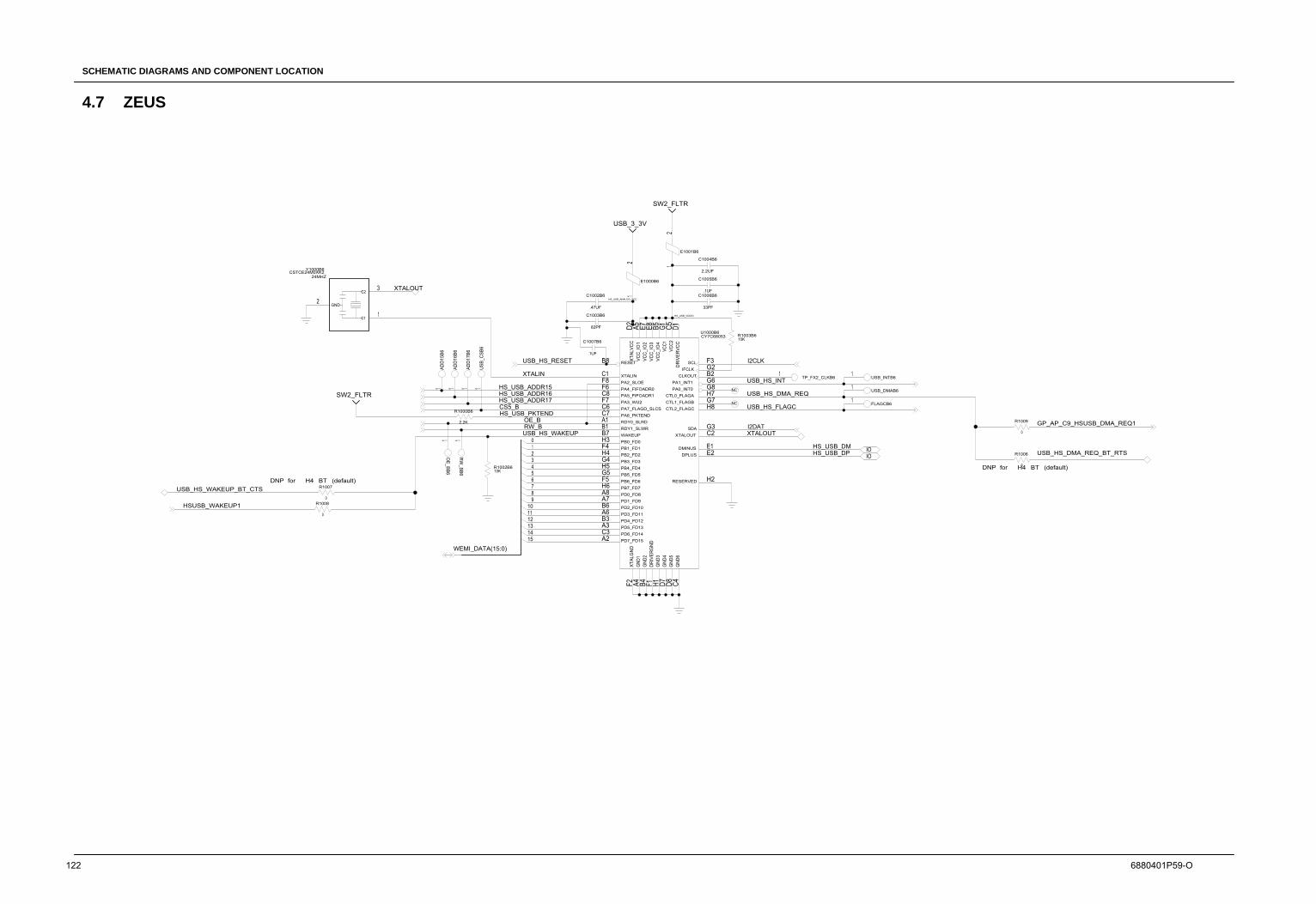
SCHEMATIC DIAGRAMS AND COMPONENT LOCATION
4.7 ZEUS
122 6880401P59-O
DNP for H4 BT (default)
DNP for H4 BT (default)
R1003B6
R1006
R1009
R1008
R1007
R1002B6
1TP_FX2_CLKB6
1
RW_BB6
1
OE_BB6
1ADD15B6
1USB_CSB6
1ADD17B6
1ADD16B6
1FLAGCB6
1USB_DMAB6
1USB_INTB6
C1007B6
R1000B6
C1004B6
C1005B6
C1002B6 C1006B6
C1003B6
21
E1001B6
21
E1000B6
2
3
1
Y1000B6
D2
C2
C1
F2
B7
B5E8E7A5 C5G1
G3
F3B8
H2
B1A1
A2C3A3B3A6B6A7A8H6F5G5H5G4H4F4H3
C6C7
C8F6
F7
F8 G6G8
G2
C4D8D7H1B4A4
D1
F1
E2E1
H8G7H7
B2
U1000B682PF
.47UF
HS_USB_VDDIO
HS_USB_ANALOG_VCC
10K
10K
3
USB_HS_WAKEUP
USB_HS_FLAGC
I2CLK
2.2UF
SW2_FLTR
HS_USB_ADDR16
CS5_B
USB_HS_INT
33PF
USB_HS_RESET.1UF
CSTCE24M0XK2
GP_AP_C9_HSUSB_DMA_REQ1
USB_HS_DMA_REQ_BT_RTS
0
4
0
HS_USB_PKTEND
USB_HS_DMA_REQ
HS_USB_DP
0
HS_USB_DM
I2DAT
CY7C68053
0
HSUSB_WAKEUP1
USB_HS_WAKEUP_BT_CTS
10
SW2_FLTRHS_USB_ADDR15
HS_USB_ADDR17
RW_B
WEMI_DATA(15:0)
0
15
5
14
8
6
21
7
24MHZ
2.2K
XTALIN
.1UF
12
9
OE_B
XTALOUT
XTALOUT
13
11
USB_3_3V
IOIO
NC
NC
C1
C2
GND
PA0_INT0CTL0_FLAGA
PA1_INT1
PA3_WU2
DRIVERVCC
VCC2
VCC1
VCC_IO4
VCC_IO3
VCC_IO2
VCC_IO1
XTALVCC
SDA
DRIVERGND
GND6
GND5
GND2
GND1
XTALGND
PD7_FD15PD6_FD14
PA6_PKTEND
PB0_FD0PB1_FD1PB2_FD2
PB6_FD6PB7_FD7
PD5_FD13PD4_FD12PD3_FD11PD2_FD10PD1_FD9
GND3
PA4_FIFOADR0PA5_FIFOADR1
GND4
PB3_FD3
RDY0_SLRD
PA7_FLAGD_SLCS
PB4_FD4PB5_FD5
WAKEUPRDY1_SLWR
SCLIFCLK
XTALOUT
CTL2_FLAGCCTL1_FLAGB
CLKOUT
RESET
PD0_FD8
DMINUSDPLUS
RESERVED
PA2_SLOEXTALIN
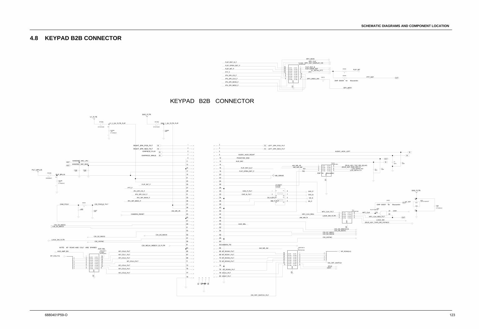
SCHEMATIC DIAGRAMS AND COMPONENT LOCATION
4.8 KEYPAD B2B CONNECTOR
6880401P59-O 123
DNP E6007 for Muscardini
NOTE: KP ROW5 AND COL7 ARE SPARES
KEYPAD B2B CONNECTOR
DNP E6009 for Muscardini
DNP for Muscardini
E6018
C2C3
C5C4
80J1
78J1
76J1
74J1
72J1
79J1
77J1
75J1
73J1
71J1
G1
5678
4321
FL813
E6008
E6009
E6007
C808
C2B1
A1U808
A2C1
U808
G1
5678
4321
FL2C6006C6007
E6003
C2509C2508
G1
87654321
910111213141516
FL1
70J1
68J1
66J1
64J1
62J1
60J1
58J1
56J1
67J1
69J1
65J1
63J1
61J1
59J1
57J1
55J1
G4J1
G3J1
G2J1
G1J1
54J1
52J1
50J1
48J1
46J1
44J1
42J1
40J1
38J1
36J1
34J1
32J1
30J1
28J1
26J1
24J1
22J1
20J1
18J1
16J1
14J1
12J1
10J1
8J1
6J1
4J1
2J1
53J1
51J1
49J1
47J1
45J1
43J1
41J1
39J1
37J1
35J1
33J1
31J1
29J1
27J1
25J1
23J1
21J1
19J1
17J1
15J1
13J1
11J1
9J1
7J1
5J1
3J1
1J1
4
3
2
1
5
6
7
8
FL6002B6
E881B6
E817B6
C896B6
21
C881B6
21
C879B6
E810B6
G1
81011124321
9765
13141516
FL810B6
G1
910111213141516
87654321
FL809B6
CSI_D9_MSEO0_BCSI_D8_MCKO
CSI_D7_MDO7CSI_D6_MDO6
NFC_CLK_FILT NUF4001MU
NFC_CLK_REQLOCK_SW_FLTR
xtal_talk_fs
NFC_CLK
NUF4001MU
LCD_DATA<17>LCD_DATA<16>
xtal_talk_clkxtal_talk_dat
TE1TE2
ZEUS_AD1_TXC_RR_DCLK0ZEUS_AD1_RXD_RR_TX
SW2_FLTR
SW2_1_8V_FLTR_FLIP
82PF
2475316C68
82PF 82PF
HANDSET_MIC_BIAS
PTT_F
IPU_SPI_CS_F
IPU_SPI_CLK_F
IPU_SPI_MOSI_F
AUDIO_JACK_LEFT
AUDIO_JACK_RIGHT
PHANTOM_GND
HANDSET_MIC_LRC
LOCK_SW_FLTR
KP_ROW0_FILT
CSI_MCLK_MSEO1_B_FLTR
CSI_D4_MDO4CSI_D3_MDO3
CSI_VSYNC
CKS_P_FILT
CSI_D2_MDO2
FLIP_INT_F
SPI1_MISO_SW
SPI1_MISO
0
PTT
SPI1_MOSI
SPI1_SS1_DISPLAY_CS
FLIP_RST_B
0
FLIP_OPEN_DETFL_INT/AJ_PTT
NUF8001MU
SPI1_CLK
V1_2_8V_FLTR_FLIP
LEFT_SPK_POS_FILT
LEFT_SPK_NEG_FILT
AUD_SEL
CSI_D5_MDO5
KP_COL0_FILT
KP_COL1_FILT
KP_COL2_FILT
CAMERA_RESET
EARPIECE_MINUS
RIGHT_SPK_NEG_FILT
RIGHT_SPK_POS_FILT
DS_N_FILT
DS_P_FILT DS_P
CKS_N
AUD_AMP_EN
KP_COL(7:0)
LOCK_SW
ZEUS_AD1_TXFS_RR_FSYNC0
NFC_CLK_REQ_FLT
74LVC1G08YZP
AUD_SEL
KP_COL3_FILT
FLIP_OPEN_DET_F
CKS_N_FILT
KP_ROW1_FILT
KP_ROW2_FILT
KP_ROW3_FILT
KP_ROW4_FILT
I2CLK_FILT
CAMERA_PD
I2DAT_FILT
ON_OFF_SWITCH_FILT
xtal_talk_dat
CKS_P
DS_N
FLIP_RST_B_F
4885534E14
NUF8001MU
IPU_SPI_CLK_F
PTT_F
xtal_talk_clk
KP_COL6_FILT
KP_COL5_FILT
KP_COL4_FILT
AUX_MIC
IPU_SPI_MISO_F
IPU_SPI_CS_F
EARPIECE_PLUS
2113946U01
FLIP_BPLUS
.1UF
FILT_BPLUS
7685268E01
2475316C68
V1_FLTR
2113946U01.1UF
0
FLIP_INT
PTT_DET
74LVC1G08YZP
SW2_FLTR
2113946U01.1UF
0
A1_INT
CKIH
2571968E03
TCM1608
FLIP_RST_B_F
FLIP_OPEN_DET_F
FLIP_INT_F
IPU_SPI_MISO_F
6543210
01234
KP_ROW(5:0)
I2DATI2CLK
ON_OFF_SWITCH
NUF8001MU
4885534E14
82PF82PF
82PF82PF
VIB_DRIVE
CSI_HSYNC
33PF
0
33PF
CAM_PCLK CSI_PIXCLK_FILT
IPU_SPI_MOSI_F
OUT
OUT
FLTR8FLTR7
FLTR8FLTR7
FLTR6FLTR5FLTR4FLTR3FLTR2FLTR1
GND
FLTR6FLTR5FLTR4FLTR3FLTR2FLTR1
IN
ININ
IN
P4
P3
S1
S2
S4
S3P2
P1
FLTR8FLTR7
FLTR8FLTR7
FLTR6FLTR5FLTR4FLTR3FLTR2FLTR1
GND
FLTR6FLTR5FLTR4FLTR3FLTR2FLTR1
IN
IN
FLTR8FLTR7
FLTR8FLTR7
FLTR6FLTR5FLTR4FLTR3FLTR2FLTR1
GND
FLTR6FLTR5FLTR4FLTR3FLTR2FLTR1
FLTR4FLTR3
FLTR1FLTR2FLTR3FLTR4
GND1
FLTR1FLTR2
OUT
IN
IN
IN
OUT
OUT
OUT
GND
VCC
FLTR4FLTR3
FLTR1FLTR2FLTR3FLTR4
GND1
FLTR1FLTR2
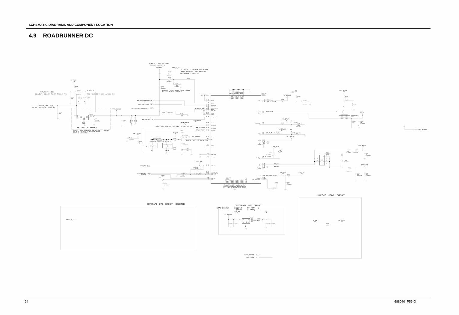
SCHEMATIC DIAGRAMS AND COMPONENT LOCATION
4.9 ROADRUNNER DC
124 6880401P59-O
NOTE:FB MUST TAP FROM C715
EXTERNAL SW3 CIRCUIT DELETED
FILT_BATTI : USE FOR HIGH POWERAUDIO AMPLIFIERS AND ALERT_VCC
RR_BATTI : USE FOR 750MA
2.775V
(RR AD4, SCHEMATIC SHEET #2)
1.875V
3.0V
2.775
3.0V
VR701 CHANGED TO 5.6V (MARLIN P14)
MD PN IS 3970350F01PIN 1 IS CLOSER TO EDGE OF BOARD
BATTERY CONTACT
HAPTICS DRIVE CIRCUIT
CURRENT LIMITED IC
CFA026: BATT CONTACTS ARE OPPOSITE FROM MD
(before 0 ohms)SW2 external triggered by SW1 FB
EXTERNAL SW2 CIRCUIT
2.775V
(COMMENT : CONNECT TO EMU TURN ON PIN)
NOTE: R706 MUST BE DIFF PAIR TO H14 AND H16
COMMENT : R708 NEEDS TO BE PLACEDNEXT TO BATTERY CONTACT
(RR SCHEMATIC SHEET #3)
C763
R736R735
C7230
C7080
R7090L7030
C7220
E7040
R7070
6
5
2
1
4
3
D7020
21
C730
R1005
L700B7
D703B7C707B7C706B7 C704B7
L704B7
C705B7
A1 B2
A3
C3C1
U701B7
43
21
G2G1
M700B7
R718B7
R707B7
R701B7
R700B7
21
VR704B7
5
4
876321 Q701B7
C709B7
R713B7
21
C715B7
R703B7
21
VR700B7C702B7
21 R704B7
C701B7
21
VR701B7 C708B7
21
C710B7
R706B7 6 5 2 1
4 3
D700B7
21
C712B7
21 R712B7
21 C716B7
E701B7
21C714B7
21 C713B7
E700B7
E702B7
R708B7
C717B7
21 C719B7
C720B7
21
C727B7C725B7
C726B7
21 C721B7
5
876321
4
Q702B7
21
R714B7
21 R715B7
G18
G16
D9C9
C7
D7
C11
B11E11
R16
B15
F6E7
R4R5
D8C8
B2C2
C10B10
G17
H18
H17
H14
H16
T18
J18
H15
L14
J14J15
B19
A19
A18
V19
W19
W18
W2
W1V1B1A2A1
P15
P17
K18
J17
R17
K16
K15
J16
F11
F15D5 U15
T14
P16
K17
E12
P18
V14
N18
R11P7G6E8F12
R18P5M15
T12
F17E9B16E5
U700B7
RR_SW1_LX1
SW1
FILT_BPLUS
82PF
7688697V04
0688044N02
BATTP_PIN_RR
82PF82PF 10UF
82PF
47UF
2113956B55
FILT_BPLUS
RR_RAW_EXT_BPLUS_PIN
RR_SW1PDRV
RR_SW1ISNSP
0
VCC_OUT
RR_SWINDRV
CONTACT
5.6V
2187893N01
1UF
FILT_BATTI
SW1_FB
0
2.2UF
RR_BATTI
RR_BATTI
2113946F08
FILT_BPLUS
BAS52
VIB_DRIVE
4.7UF
V_VIB
HAPTICS_EN
SW2
2113956B55
2.2UH
2175511A01
CDZT2R5_6B
VSIM_EN
SC55112VH
.05
.02
EXT_SW1_SWITCH_PIN
LM3671
2.2UF
NSS35200CF8T1G
0
0
5.6V
VCC_OUT
2113944E20
CDZT2R5_6B
2113956B55
0
56PF
22UF
RR_V1_OUTPUTRR_V1_IN
SW2_MEM_FB
2113946F08
2.2UF
RR_V2_DRV
0
5175771A73
V_VIB_IN
0
0613952Y66
USB_VBUS_URTSIVHOLD_EXT_EN
1%
V4
V3
V1
VSIM
V2
FILT_BPLUS
16V
68UF
68UF4805656W46
22UF
RR_V4_IN0
0613952Y66
DSM2
FLASH_STROBE
USB_3_3V
FILT_BPLUS
00613952Y66
4.7UH2571104B04
2113946F0822UF
.1
SW3
RR_LX3
RR_FB3
BAT960
FILT_BPLUS
V_VIB
0613952Y66
4.7UF
2175511A01
1UF
7685268E01
SW3_CAPS
22UF
0689774Y02
FILT_BPLUS
5.6K
BATTERY_TEMP
BATTERY_ID
V1_FLTR
00613952Y66
BATTI
FILT_BPLUS
SW3
2187893N01
4870370A33
FILT_BPLUS
FILT_BPLUS
0
V2_IN
0
4.7UF
RR_VDRV4_5_PIN
2175511A01
BAT9604870370A33
2175536A01
RR_MOBPORTB_PIN
7685268E01
VHOLD_OUT
0613952Y66
0
SW1_FB
RR_VUSB
82PF
82PF
RAW_B_PLUS
82PF
7685268E01
47UF
4809607E17
.1UF
BATT_ID_FLTR
4813970M62
SI5441DCT1
BAT_DET_IN
FILT_BPLUS
4.7UH
NC
NC
NC
IN
NC
SW1ISNSP
NC2_2
NC2_3
NC3_1
AGND5
AGND6
AGND7
VSIMVSIM_EN
VCC_OUT
BPLUS
BATTI
PSRC1
RAWEXTBPLUS
MAIN_FET
ISENSECHRGC
SW1ISNSN
NC2_1
NC3_2
NC3_3
NC4_1
NC4_2
NC4_3
MOBPORTB
PGND3
FB3
USB_VBUS_URTSI
VHOLD_EXT_IN
V_VIB
AGND_ESD2_2
BST_IN
LX3
V_VIB_IN
VUSB
AGND8
V3_VSIM_IN
BATT_DET_IN
NC1_3
NC1_2
AGND1
AGND2
VHOLD_EXT_EN
DGND1_1
DGND2
DGND3
AGND3
AGND4
V4_IN
FB2
VDRV4_5
V2_FB
AGND_ESD2_3
AGND_ESD2_4
AGND_ESD1
AGND_ESD2_1
PSRC2
VUSB_IN
V1_IN
V4
VHOLD_OUT
VMMC_DRV
DGND1_2
PGND1
DGND_TEST
LX2
V3
V1
V2_DRV
FB1
PGND2
SW1NDRV
SW1PDRV
NC1_1
BATTP
VMMC_FB
IN
IN
IN
NC
NC
FB
SW
GNDEN
VIN
NC
PIN1PIN2 PIN4
PIN3
GND1
GND2
NC
NC
NC
NC
IN
IN
IN
IN
OUT
OUT
OUT
OUT
IN
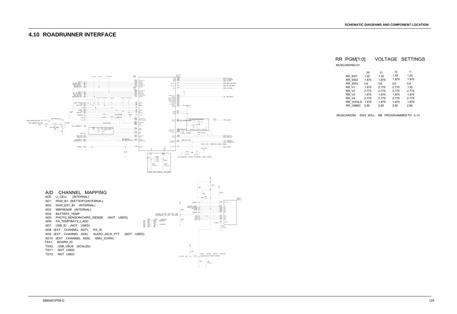
SCHEMATIC DIAGRAMS AND COMPONENT LOCATION
4.10 ROADRUNNER INTERFACE
6880401P59-O 125
ID1: 47K -- DNP - Brightwater
ID6: DNP -- 47K --ID5: 47K -- 10K --ID4: 100K -- 47K -- MuscardiniID3: 47K -- 47K --ID2: 47K -- 100K --
R729 -- R730 -- PRODUCTAD5: PHOTO_SENSOR/CHRG_ISENSE (NOT USED)AD6: PA_TEMP/BATT_I_ADC
AD1: RAW_B+ (BATTERY)(INTERNAL)
MAY REQUIRE VALUES DIFFERENT THAN 0-OHMS
PLACE R739 WHEN NOT USING SIGNAL
SEPARATE ISOLATED GROUNDS
VALUES ON R729 AND R730 AREDETERMINED BY HSID DOCUMENT
scaling network DNP for Muscardini
AD9 (EXT CHANNEL AD8): AUDIO_JACK_PTT (NOT USED)
MUSCARDINI SW3 WILL BE PROGRAMMEDTO 5.1V
MUSCARDINI=01
RR PGM[1:0] VOLTAGE SETTINGS
AD0: LI_CELL (INTERNAL)
RR_V3
RR_VHOLD
00RR_SW1
2.80RR_VMMC
RR_V4
RR_SW2RR_SW3
RR_V2RR_V1
1.875
1.8755.6
2.775
1.8752.775
1.551.875
2.775
2.7751.8752.80
1.8751.2001
5.6
1.8752.775
2.80 2.80
1.875
5.62.775
1.875
1.551.875
10
2.775
2.7751.8752.775
1.55
1.20
1.8752.775
5.61.875
11
TSY1: NOT USED
AD3: MBPSENSE (INTERNAL)AD4: BATTERY_TEMP
AD2: RAW_EXT_B+ (INTERNAL)
DNP
PLACE XTAL CIRCUIT FOR NOW
TSX1: BOARD_ID
TSY2: NOT USED
A/D CHANNEL MAPPING
TSX2: USB_VBUS (SCALED)
AD10 (EXT CHANNEL AD9): EMU_ICHRG
AD8 (EXT CHANNEL AD7): PA_IDAD7: USB_ID (NOT USED)
RF BOARD ALONEPLACE R702 WHEN POWERING
C745
C744
R737
C759R754
R756
R755
1
TP_TXB7
R723
R722B7C731B7
2
31
Q703B7
1
PRI_INTB7
1
SEC_INTB7
C732B7
C733B7
C734B7
R742B7
C742B7
21 C738B7
21 R732B7
C739B7
21 C741B7
C735
R724
21 R727B7
21 R725B7
1
TP_SEC_CEB7
1
TP_BITCLK1B7
1
TP_RX1B7
1
TP_BITCLK0B71
TP_RX0B7
U12
U11
F16
C16
G12
L15
L13
G13
E17
C18
G15G14
E18
D18D6
E14
U17U16V17
N14M14
E16
C5
E6
T11
E13C14
T17T15U18
R15T16
E15
T5R3R2
B18C17
D16F14
F5
N15N16
K14R12
B14
M18M17M16
L17
L16
D14C15
V18
M13
B5
G5
F13
D17
D15
P11M2
C3
C6
B6
B17
U700B7
T13U13V13P12
R13
V16
P14R14V15N13U14P13
U700B7
21
C737B7
21
C736B7
12Y700B7
R745B7
R738B7
R741B7
R730B7
R729B7
21
C743B7
82PF
BATTERY_TEMPPHOTO_SENSOR
PA_TEMP
ADTRIG
82PF
47K
V4
100K
TSX1TSX2TSY1
SW2
VCC_OUT
XTAL1
USER_OFF_PIN
LI_CELL
RR_LCELL_BYP
2187893N01
CD_CAP_ROADRUNNER
0613952Y66
FILT_BPLUS
EOL_INTERRUPT
DTC144EM
000613952Y66
2113956B55
33PF
EMU_PWRON_RR_ON2
V4
RX0
RR_ON2B_BASE
220K
EMU_USBPWR_RR_ON2
68PF
SC55112VH
2113944E15
5175771A73
SC55112VH
32KHZ
KP_LED_PWM
XTAL2
CI_BLUE
MOD_OUT
CI_REDCI_GREEN
PRI_SPI_CLKPRI_SPI_MOSI
PRI_CE
MUX_OUT
2113944E1518PF
32.768KHZ
4809995L15
BITCLK0
0613952Y66
2187893N01
39K
68PF
LVS
1UF
200K
18PF
0
0
SW2
V4
2.2UF
4.7UF
V1
LV_DETECT
SW2
EMU_PWR_ON_C
5.6K
47K
RESETMCU_B
5175771A73
2.2UF
16.8MHZ
FSYNC1
TX
PRI_SPI_MISO
PRIMARY_INT
RR_USB_ID
DISP_LED_PWM
2.7K
PA_ID
ICHRGE
.1UF
PTT_DET
2113946U01
392K
75K
20K
V2
2175536A01
RR_RESETMCU_BRR_RESETB
WDI
BG_BYP10K
CID_PWM
AUDIO_JACK_PTT_DET_SCALED
.1UF
SW2
FSYNC0
SEC_CESEC_SPI_MISOSEC_SPI_MOSISEC_SPI_CLK
SECONDARY_INT
RX1BITCLK1
STANDBYRR_LVS
RR_STANDBY
0613952Y66
ON
RR_ON2_PIN
BG_BYP_ROADRUNNER
1UF
47UF
POWER_FAIL
CS_OUTVPP_OUT
USEROFF
TS_BYP
TSY2
OUT
OUT
OUTOUT
OUTOUT
OUT
OUT
OUT
OUT
OUT
OUT
OUT
OUT
OUT
IN
IN
IN
IN
IN
IN
IN
ININ
IN
ININ
INPRI_MISO
MAIN_DIG_VCC
LCELL_BYP_1LCELL_BYP_2
CLK_32KHZ
DIN_UTXDI
USER_OFF
SE0_IN
VICR
USB_VP
USB_DIG_VCC
LED2_DRV
LED1_DRV
XTAL1
XTAL2
RTC_GND
POWER_FAIL
RX1
RX0
PRI_DIG_VCC
SEC_MOSI
WDI
ONBON2B
MCLK
BG_BYP
PGM4PGM1PGM0
TX_ENB
LEDB
RESETMCU_BRESETB
MOD
EOLI
LVS2
BITCLK1
FSYNC1
TX
BITCLK0
SEC_MISO
USB_ID
USB_DP_UTXDOUSB_DM_URXDI
CS_OUTVPP_OUT
LI_CELL
CD_CAP
XRXD_URTSOUSB_VM_URXDO
LEDRLEDG
FSYNC0
INT_SECSEC_SPI_CLK
INT_PRIPRI_SPI_CLK
SEC_CESEC_DIG_VCC
PRI_MOSI
PRI_CE
LVSSTANDBY
MAIN_DIG_GND
CLK16_8
MUX_CTRL
TS_BYP
TSX1
AD9AD8
TSY1
AD7AD6AD5AD4
TSY2
TSX2
AD_TRIGIN
IN
INININ
47K
47K
IN
IN
OUT
OUT
IN
OUT
OUTOUTOUT
INININ
OUTOUT
OUT
OUT
IN
IN
IN
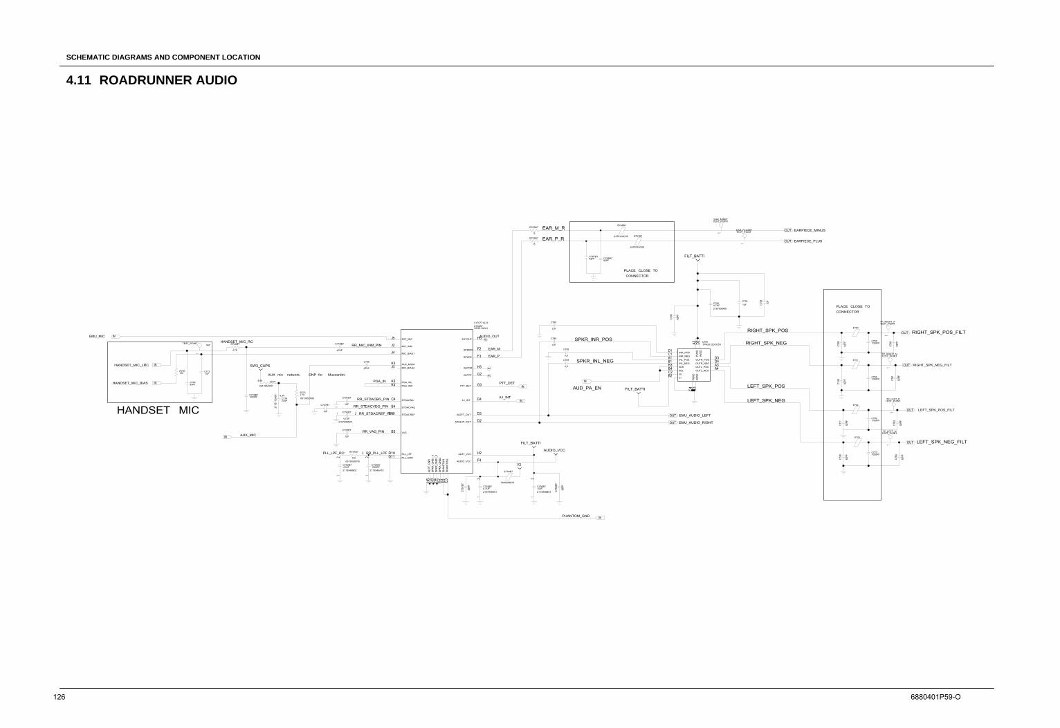
SCHEMATIC DIAGRAMS AND COMPONENT LOCATION
4.11 ROADRUNNER AUDIO
126 6880401P59-O
AUX mic network, DNP for Muscardini
PLACE CLOSE TO
PLACE CLOSE TO
CONNECTOR
CONNECTOR
HANDSET MIC
R750 C772
C770
C769
C766
C765
C764
C762
C761
C760
C749
1
TP_RIGHT_N
1
TP_LEFT_N
1
TP_LEFT_P
1
TP_RIGHT_P
C774
C798
R773
R774
1
MIC
E702
E703
E701
E700
E767B7
E768B7
C728
C771
C740
C795
C799
C794
C793
C792
C790
C785
B3B4
A2C4
D3D4A3A4
D1C1A1B1
B2C2
D2C3
U700
C789
C788
C746B7
C757B7
C758B7
1
EAR_MINB7
1
EAR_PLUSB7
C768B7C767B7
R753B7
R752B7
R748B7
B3
B4
E10
C4
F3
F2
E2H4G4
G3
D10D11
E3E4
K4K5
J2
J3
J4
H5J5
K3
F4
D2
G2
H3
H2
H6
D3
D4
U700B7
21
C756B7
E704B7
21
C755B7
21
C754B7
21
C750B7
21 R751B7
21 C752B7
C751B7
C747B7
C753B7
C748B7
HANDSET_MIC_BIAS
TEST_POINT
HANDSET_MIC_LRC
100
.47UF
RR_MIC_INM_PIN
SW3_CAPS
HANDSET_MIC_RC
1000PF
.1UF
0613952X91
AUX_MIC
5175771A73
2475316C05
2475316C05
2.7K0613952X83
1UF
1UF
SPKR_INR_POS1UF
1UF
4.7UF2187906N01
FILT_BATTI
TEST_POINT
.1UF
TEST_POINT
EARPIECE_PLUS
RR_STDACVDG_PIN
.47UF
22UF
2175110A01
AUD_PA_EN FILT_BATTI
6.3V
PTT_DET
A1_INT
AUDIO_VCC
PHANTOM_GND
RR_STDACBG_PIN
RR_STDACREF_PIN
82PF
7685268E01
82PF
SC55112VH
AUDIO_OUT
EAR_P
EMU_AUDIO_RIGHT
EMU_AUDIO_LEFT
RR_VAG_PIN
2187906N01
82PF
LEFT_SPK_POS
.1UF
.1UF
PGA_IN
2113945B02
0613952R16
4.7UF
43K
10UF
.01UF
PLL_LPF_RC
2113956B54
2113945A101500PF
.1UF
2187906N01
V2
FILT_BATTI
15EARPIECE_MINUS
EMU_MIC
LEFT_SPK_NEG
82PF
82PF
EAR_M_R
1UF
EAR_M
RR_PLL_LPF
4.7UF
82PF82PF
EAR_P_R
TPA2012D2YZH 82PFRIGHT_SPK_NEG
15
LEFT_SPK_POS_FILT
TEST_POINT
82PF
82PF
TEST_POINT
TEST_POINT
TEST_POINT
82PF
RIGHT_SPK_POS_FILT
82PF
RIGHT_SPK_NEG_FILT
RIGHT_SPK_POS
1000PF
1000PF
82PF
LEFT_SPK_NEG_FILT
1000PF
4.7K
5.6K
82PF
SPKR_INL_NEG
1000PF
OUT
OUT
IN
IN
IN
IN
IN
IN
OUT
OUT
OUT
OUT
IN
PVDD
G1G0SDLSDR
INL_POSINR_NEGINR_POS
OUTL_POSOUTR_NEG
AGND
PGND
OUTL_NEG
OUTR_POSINL_NEG
AVDD
NC
NC
IN
OUT
OUT
NC
A1_INT
EXT_MIC
MIC_INM
MIC_BIAS1
PGA_INRPGA_INL
AUX_MICMMIC_BIAS2
STDACBG
ALRT_GND
VAG
ALRT_VCC
SPKR_GND1_1
SPKR_GND2
SPKR_GND1_2
PHANTOM1
PHANTOM2
EXTOUT
SPKRM
ALRTM
ALRTP
PTT_DET
ALEFT_OUT
ARIGHT_OUT
PLL_GND
STDACREF
PLL_LPF
AUDIO_VCC
SPKRP
STDACVAG
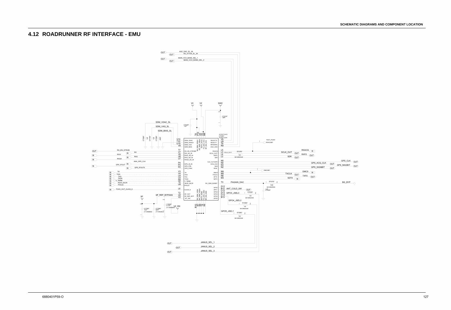
SCHEMATIC DIAGRAMS AND COMPONENT LOCATION
4.12 ROADRUNNER RF INTERFACE - EMU
6880401P59-O 127
R757B7
C778B7
R8U3U4V4V3
M5
V5T4
N2
N6
V2U2T2
V9U9
M3
L2
T10V10
U10V8
L3
U5R6
U7U6V6V7
L4
L5
R7R10
T6 P10
T3
T7
T9
M6K6
U8
N3
T8
P2P3P4
B13C13D13C12B12D12
M4
N5
L6
R9
N4
U700B7
1 DMCSB7
1 RXACQB7
21
C781B7
C703B7
C779B7
C777B7
C776B7
21
C780B721
C775B7
C700B7
21 R761B7
21 R758B7
21 R759B7
21 R760B7
.1UF
GPO3_JSEL3
GPO4_JSEL2
GPO5_JSEL1
MAIN_VCO_BAND_SEL_2
ANT_COLD_SW
TXFS
0613952X49100
5175771A73
SC55112VH
RX_EN_STROBRXI
GPS_IFOUT
ANA_GPS_CLK
GPS_IFOUTX
TXI
RXQRXQX
RXIX
V_TERM
TXQTXIX
SDTX
TXCLK
GPS_SIGNBITGPS_MAGBIT
GPS_ACQ_CLKGPS_CLK
SDR
SCLK_OUT1
RXFS
TXQX
TCXO_OUT_CLK33_6
SF_REF_BYPASS
PHCLKINCR_DECR PAGAIN_DAC
SDM_VDAC_SL
JANUS_SEL_3
JANUS_SEL_2
JANUS_SEL_1
MAIN_VCO_BAND_SEL_1
RX_ATTEN_SL_JN
SCLK_OUT
DMCS
AGC_DAC_SL_JN
SW2
SF
2113944E2282PF
2113956B5410UF
1000613952X49
1000613952X49
4.7UF
V2
18PF
100K0613952R25
BG_BYP
.1UF
SDM_VAG_SL
1000613952X49
TEST_POINT
V2
RXACQ1UF
1UF
.22UF
SDM_BIAS_SL
2113956B55V2_RX
OUT
OUT
OUT
OUT
OUTOUT
OUTOUT
IN
INININININININ
ININ
IN
IN
ININ
IN
OUT
SDM_VDAC0SDM_VAGSDM_BIAS
RX_EN_STROBERXI_AD_IN
GPS_IFINGPS_49_IN
GPS_IFINX
TXI
RXQ_AD_INRXQX_AD_IN
RXIX_AD_IN
SDM_VDAC
RX_SDM
_VSSA
RF_SSI_VCC
TX_DAC_VCC
RXTX_AVCC
RX_SDM
_VDDA1
SF_VIN GPO5GPO4GPO3
GPO1GPO0
V_TERM
TXQTXIX
SDTXSFTXTXCLKDMCS
SIGNMAG
ACQ_CLKCLK_OUTGPS
SDR
SELECT1
SCLK_OUTRXACQ
AGC_DACRFSTEPA
RXFS
SELECT2
TX_DAC_GND
RX_SDM
_VDDA
TXQX
CLK33_6
SF_OUTSF_REF_BYP
GPO2
PHCLK
RF_SSI_GND
RXTX_AGND
RX_SDM
_VSSA1
INCR_DECR RX_SDM_BGREF
IN
IN
IN
OUTOUT
OUT
OUTOUT
OUTOUT
OUTOUT
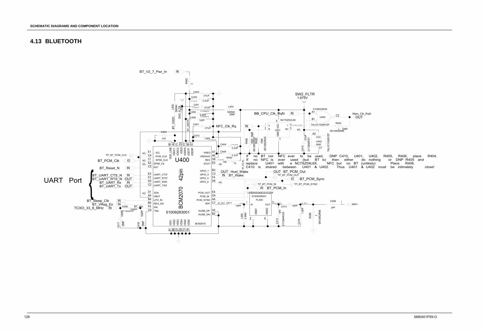
SCHEMATIC DIAGRAMS AND COMPONENT LOCATION
4.13 BLUETOOTH
128 6880401P59-O
If no BT nor NFC ever to be used, DNP C410, U401, U402, R405, R406, place R404.If no NFC is ever used (but BT is) then either do nothing or DNP R405 andreplace U401 with a NC7SZ04L6X. NFC but no BT (unlikely): Place R406.C410 is shared between U401 & U402. Thus U401 & U402 must be intimately close!
UART Port
DNP
DNP
DNP
DNP
DNP
BT_UART_Tx
51009283001
46
5
3
21
U401
R406
C2B1
A1
U402
A2
C1
U402
R499
1 M401
C416
C417
C404
C406
R402
C402
L403
C415
L402
C409
C499
L400
31
42
FL400
C414
C413C411
R400
E5
F5
F6F3E6D7B6A1
A6A7
B7 E7F7D3F1A3B1
A5
C2D2F2E3
C6
E2C1
D1
E1
C5
C7
D6
B5A4
E4D4
C4
B4
A2B2
D5F4
B3C3
U400
R405
R404
C410
C412
C407
C408
C400
C405
C403
1TP_BT_PCM_CLK
1 TP_BT_PCM_IN
1TP_BT_PCM_OUT
C401
1 TP_BT_PCM_SYNC
SW2_FLTR
SW2_FLTR
BT_V2_7_Pwr_In
0
BB_CPU_Clk_RqN
.01UF
Host_WakeBT_UART_CTS_N
BCM2070
42pin
BT_Wake
NC7SZ02L6X
5109522E94
BT_VDDTF 10PF
.1UF
BT_VDDC
10PF
0613952R25
2113945F07
0613952R25
BT_Clk_Rq15K
.01UF
2170282F346.8PF
2113944E10 560NH
NFC_Clk_Rq
2.2UF
1%
LFB2H2G45CG1C026
BT_RFP1
0613952R66
BT_PCM_In
1.5PF
0
2PF10PF
1.875V
74LVC1G08YZP
BT_PCM_Sync
BT_PCM_Out
3.3NH 1PF
2113944V03
91009256001
2171410C01 2.2UF
BT_Ref_ResBT_PCM_Clk
BT_Reset_N
BT_UART_Rx
BT_Sleep_Clk
2113945F07
Main_Clk_RqN
100K
2.2UF
BT_XIn100PF
BT_UART_RTS_N
100PF
BT_VReg_En
2113944E23
2171410C01
.01UF
1.875V
560NH
.01UF
BT_VReg_Out
0613952R66
74LVC1G08YZP
BT_RFFOut
TCXO_33_6_MHz
0
BCM2070
10PFBT_RFFIn
100K
BT_NFC_Clk_RqN
BT_RFP
100PF
VREGVREGHV
RESXOUT
HUSB_DN
UART_TXDGPIO_6GPIO_5
REG_EN
VSS1
VSS2
VSS3
VSS4
XINTM2
VBATLPO_IN
SDA
UART_RXDUART_RTS*
RST
UART_CTS*
SPIM_CSSPIM_CLKPCM_CLKSCL
VDD_USB
VDDC1
VDDC2
VDDO
VSS6
VSS5
HUSB_DP
RFP
PCM_INPCM_SYNC
PCM_OUT
GPIO_1GPIO_0
VDDTF
VDDPX
VDDRF
IN
OUT
IO
IN
NC
AB
GND
VCC
NCY
GND
VCC
NC
NC
IN
NC
GND2
IN
GND1
OUTIN
INNCNC
NC
INOUTINOUT
INOUT
IN
OUTIN
IN
IO
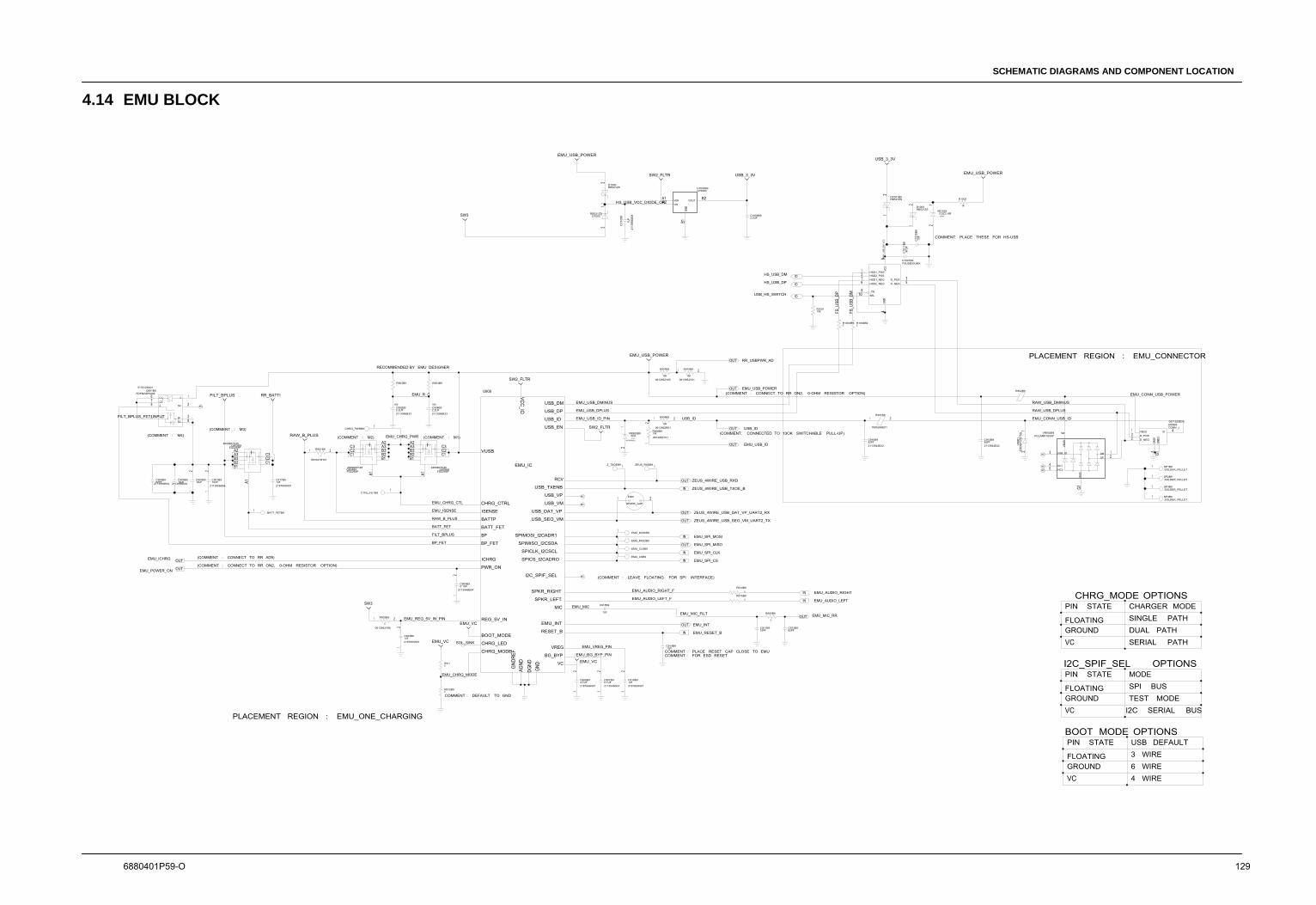
SCHEMATIC DIAGRAMS AND COMPONENT LOCATION
4.14 EMU BLOCK
6880401P59-O 129
PCB rev10, phone rev Pilot2
(COMMENT : M2)
COMMENT: PLACE THESE FOR HS-USB
(COMMENT : CONNECT TO RR AD9)
RECOMMENDED BY EMU DESIGNER
PLACEMENT REGION : EMU_CONNECTOR
(COMMENT : M1)
COMMENT : PLACE RESET CAP CLOSE TO EMUCOMMENT : FOR ESD RESET
I2C_SPIF_SEL OPTIONS
CHRG_MODE OPTIONSCHARGER MODE
COMMENT : DEFAULT TO GND TEST MODE
U900
GROUNDVC
BOOT MODE OPTIONSPIN STATE
VCGROUNDFLOATING 3 WIRE
4 WIRE6 WIRE
VC
PIN STATE
FLOATINGGROUND
PIN STATE MODESPI BUS
SINGLE PATH
SERIAL PATH
I2C SERIAL BUS
DUAL PATH
FLOATING
USB DEFAULT
(COMMENT : LEAVE FLOATING FOR SPI INTERFACE)
PLACEMENT REGION : EMU_ONE_CHARGING
(COMMENT : CONNECT TO RR ON2, 0-OHM RESISTOR OPTION)
(COMMENT: CONNECTED TO 10OK SWITCHABLE PULL-UP)
(COMMENT : CONNECT TO RR ON2, 0-OHM RESISTOR OPTION)
(COMMENT : M4)(COMMENT : M3)
C917B9C908B9 C909B9
R1002
21
VR1003
21
D1001B9
21
D1003
C1009B9
B2A2A1
B1
U1002B9
CC1008
21
D1002
21
D1000
1BATT_FETB9
4
25
83
76 1
Q901B9
1EMU_CSB9
1EMU_CLKB9
1EMU_MISOB9
1EMU_MOSIB9
R915B9
R914B9
1 SP4B9
1 SP3B9
1 SP2B9
1 SP1B9
R905B9
C912B9C911B9
6
3
54
G1
21
VR902B9
C915B9
1 4
G15
32
J900B9
R1001
21
VR901
R1004B9R1003B9
C1011B9
C1010B9
9
10
2
6
1
7
4
35
8
U1001B9
R912B9
R911
C914B9
1ZEUS_RXDB91Z_TXOEB9
21 E900
1CHRG_PWRB9
1CTRL_FETB9
C902B9
R903B9
C910B9 C913B9A2A3B3B2B1
A1
C3C2C1
Q905B9
A2A3B3B2B1
A1
C3C2C1
Q904B9
A2A3B3B2B1
A1
C3C2C1
Q902B9
21 R901B9
E902B9
21E901B9
21 R910B9R907B9
21
VR900B9
21
R906B9
21 R909B9
21
C916B9
21
C907B9
21
C906B9
C904B9
21
C903B9
21 R902B9
R904B9
21
C905B9
21
C901B9
21
C900B9
RR_BATTIFILT_BPLUS
USB_3_3V
SW2_FLTR
EMU_VC
SW3
SW3
EMU_VC
EMU_VC
RAW_B_PLUS
SW2_FLTR
EMU_USB_POWER
USB_3_3VSW2_FLTR
EMU_USB_POWER
EMU_USB_POWER
RR_USBPWR_AD
4809807C45FDZ293P
1UF2187893N01
2187893N011UF
EMU_REG_5V_IN_PIN
2113946B04
BP_FET
FILT_BPLUS
10UF2113956B5482PF
82PF
10UF2113956B542113956B5410UF
EMU_CHRG_PWR
0
0
1K
3.845V
.1UF
FSUSB30UMX
FS_USB_DM
FS_USB_DP
RB521ZS
2113956A51 2.2UF
U1001_USB_SW
_VCC
HS_USB_DP
.47UF
RB521ZS
2113956B33
RCLAMP1654P
ESD9X12ST5G
RAW_USB_DMINUS
RAW_USB_DPLUS
EMU_AUDIO_RIGHT_F
EMU_AUDIO_LEFT_F
EMU_MIC1UF
4809807C45
EMU_CHRG_CTL
EMU_ISENSE
RAW_B_PLUS
BATT_FET
SPARK_GAP
33PF
EMU_SPI_CLK
EMU_MIC_FILT
EMU_VREG_PIN
EMU_MIC_RR
.1UF
1UF2113946B04
EMU_SPI_CS
EMU_SPI_MISO
0616416H01
10K
EMU_USB_DMINUS
0613952Y01
5178126A01
2187893N01
USB_ID
0
EMU_AUDIO_LEFT
EMU_BG_BYP_PIN
EMU_CHRG_MODE
CONN_J
4.7UF
10K
0
0613952Y01
0
2187906N01
2.2UF
.1
0.1UF
82PF
FDZ293P
10K
5.6V4870359A02
0
0613952Y660
EMU_AUDIO_RIGHT
FDFMA2P029Z
EMU_USB_ID
EMU_RESET_B
EMU_INT
SOL_SINK
0.1UF
EMU_SPI_MOSI
USB_ID
EMU_POWER_ON
SOLDER_PELLET
SOLDER_PELLET
SOLDER_PELLET
SOLDER_PELLET
0971529E05
EMU_CONN_USB_POWER
82PF2113944E22
16V
2113944E22
7685268E01
EMU_CONN_USB_ID
0
16V
1 1
EMU_R_C
2.2UF2113956B33
FDZ293P4809807C45
FILT_BPLUS_FET_INPUT
EMU_ICHRG
ZEUS_4WIRE_USB_TXOE_B
ZEUS_4WIRE_USB_RXD
0613952R01
EMU_USB_DPLUS
EMU_USB_ID_PIN
RB521ZS
ZEUS_4WIRE_USB_SEO_VM_UART2_TX
ZEUS_4WIRE_USB_DAT_VP_UART2_RX
EDZ
0613952Y0515K
LP5900
1UF
HS_USB_VCC_DIODE_OR
EMU_USB_POWER
RB521ZS
HS_USB_DM
USB_HS_SWITCH
10K
CDZ3_6B
OUT
OUT
OUT
OUT
NC
NC
OUT
OUT
OUT
EMU_IC
USB_TXENB
USB_VP
USB_VM
USB_DAT_VP
USB_SEO_VMBATTP
ISENSE
USB_EN
USB_DM
USB_ID
USB_DP
VCC_IO
I2C_SPIF_SEL
SPICS_I2CADRO
BATT_FET
BP
BP_FET
SPKR_RIGHT
SPKR_LEFT
PWR_ON
ICHRG
GND
GNDREF
AGND
DGND
EMU_INT
MIC
SPICLK_I2CSCL
SPIMISO_I2CSDA
RESET_B
VREG
BG_BYP
VC
BOOT_MODE
CHRG_LED
CHRG_MODE
REG_5V_IN
CHRG_CTRL
SPIMOSI_I2CADR1
RCV
VUSB
IN
IN
IN
IN
IN
IN
OUT
OUT
OUT
NC
OUT
OUT
VOUT
GND
VINVEN
S
NC
AC1C2G
D2D1
NC
NCNC
NC USB_ID
DP
NC1
DM
GND
NC2
VBUS
D_NEGD_POSVBUS ID
GND1
GND2
IO
IO
IOD_POSD_NEG
HSD1_POSHSD2_POSHSD1_NEGHSD2_NEG
_OESEL
GND
VCC
IN
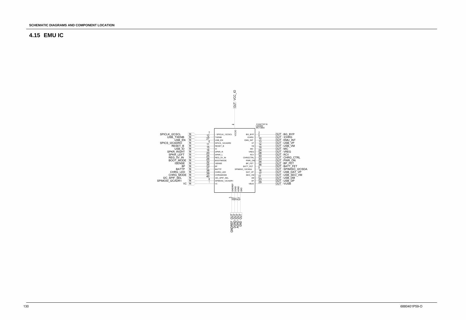
SCHEMATIC DIAGRAMS AND COMPONENT LOCATION
4.15 EMU IC
130 6880401P59-O
24
1314
4
1 29
2712
1820
8
9
6
7
17
11
2528
33
19
32
15
5
40
3 G1
10
2321
22
1639
30
38
3435
26
2
3736
31
U900B9
SPICLK_I2CSCL BG_BYP
EMU_INTUSB_VP
CHRG_CTRL
BATT_FET
VCC_IO
USB_VM
USB_SEO_VMUSB_DAT_VP
MICVREGRCV
USB_TXENBUSB_EN
SPICS_I2CADRO
CHRG_LED
DGND
AGND
GNDREF
RESET_B
REG_5V_INBOOT_MODE
USB_ID
VC
CHRG_MODEUSB_DM
BP_FET
BATTPBP
ISENSE
GND
ICHRG
SPIMOSI_I2CADR1I2C_SPIF_SEL
SPKR_LEFTSPKR_RIGHT
VUSBUSB_DP
PWR_ON
SPIMISO_I2CSDA
5109773F18
MC13883
OUTOUTOUTOUTOUT
INININ
OUT
ININININININININININ
OUT
ININININ
IN
OUT
OUT
OUT
OUT
OUT
OUTOUTOUTOUTOUTOUTOUTOUTOUTOUTOUT
MICVMVP
SPIMISO_12CSDABATT_FETBP_FETPWR_ON
CHRGCTRLRCV
VBUSDPDM
SEO_VMDAT_VP
GND
ISENSEBOOTMODEREG_5V_INSPKR_L
CHRGMODECHRG_LEDBATTPBP
TXENBSPICLK_12CSCL
SPKR_RIDRESET_BSPICS_12CADR0USB_EN
VC
AGND
BG_BYPICHRG
EMU_INT
VCCIO
I2C_SPIF_SEL
GNDREF
DGND
SPIMOSI_12CADR1
VREG
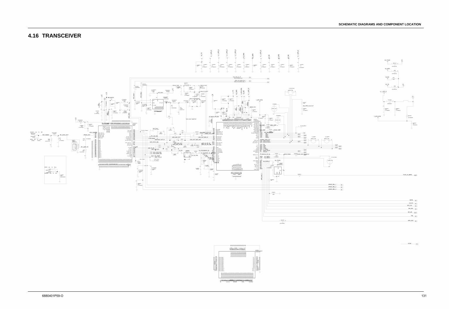
SCHEMATIC DIAGRAMS AND COMPONENT LOCATION
4.16 TRANSCEIVER
6880401P59-O 131
M502B10 only for BW
(rotated contact)
M500B10 only for BW
M5000 only for Musc.
M5020 only for Musc.
Mon May 03 15:27:44 2010
84009289002.cpm
transceiver
<
1
L500
M50203987977Y02
ANT_FEED413987977Y02M502B10
M50003987977Y02
M500B103987977Y02
.5PF
1
1
C510
R641
21
L502
C500
R530R531
L513
C225
R216
R215
L501B10R630B10
R629B10
R696B10
C223B10
C222B10
21
E_GPS_IFB10
21
E_TXQB10
21
E_TXIB10
C696B10
C695B10
C508B10
C507B10
C506B10C509B10
R503B10
21
C661B10
R661B10
C678B10
L601B10
C218B101 TP_RX_ENB102
1E_RXQB10
21E_RXIB10
C694B10
L694B10
C231B10
C676B10
21
R324B10
1ASWB10
21
TP_SLTSTB10
1 TP_PAIDB10
21C213B10
21
C214B10
21
R212B10
1 TP_RF_ATTNB101 TP_LNA_ENB10
R357B10
21C323B10
21
R326B10
21
R323B10
21
C325B10
21
C322B10
21
C326B10
21
C328B10
21
C327B10
21
C347B10
21
L641
R631
R632B10
C230B10
21
C677B10
21E601B10
21
C221B10
21
C303B10
21
C526B10
21
C518B10
21
C521B10
21
C514B10
21
C515B10
L639B10L640B10
21L503B10
21 C600B10
21 C601B10
21
C634B1021
C216B10
21
C215B10
21
C640B10
21
C639B10
21
C693B10
21
C692B10
21
C691B10
21C517B10
21
4 3
U505B10
R660B10
21
C501B10
21
E331B10
21
E332B10
E659B10
C332B10
C331B10 21
C321B10
C330B10
5
9
7
8
1
6121110432
U200B10
21
E656B10
21
C233B10
21
C234B10C235B10
21
C236B10
21
C224B10
21
C228B10
21
C502B10
21
C503B10
C229B10
21
C305B10
21
C301B10
21 R650B10
21 C217B10
21 C219B10
21 C670B10
21
C650B10 4
3
21
Y002B10
21 R211B10 21
C212B10
21
R653
21
C504B10
21 C5
05B10
21
C651B10
4
3
12
J500B10
21
C568
21 R654
L653
21 R652
21 R651B10
P2
B13B14B15D14C14
B7
C7
B4B3
C4
B6 D16
G16F16
L16M16
T8
R6T5
T6
R4
L15
B2
E3
J15
C2
E2
J16
D2
F3
H15
D3
F2
H16
G3
K2
J2
K15
L3
L2 G15
R9
T9
E16
G2
T7
T2T3
H2
M2N2
R2 T4
P4P3
R8
B12C13B11C12
M7
F15
R7
T13
T12
T15T14
R16
R12
K16 N16P16
T11
R11
R10
P15
T16
M15
B9 B10
C10
C11
B8
T10
N15
H3
R5
C16B16
B5
C5
U600B10
I8
G9H4 H1
K9K8
A8
F9
D5B5C5
K6
K4G6
G5
E9D9D8
F6
G1
C6
A6
H9
G3
K2K1
G4
D3
B4B3B2B1
D1K7K3I9I7I6I5I4I3
A9
I2I1H8H7H6H5H3H2G7C1
A7
G2F8F7F5F4F3F2F1
E8E7
A4
E6E4E3E2E1D7D6D4D2C9
A3
C8C7G8C4
C3C2B9B8B7B6
A2
A5A1
K5
E5
U500B10
G7G6
F12F11
R14
R13
P14
F10
N3M3K3J3E15
D15D4C9C8C6
F9
M12
M11
M10M9M8M6L12
L11
L10L9
F8
L8L7L6K12
K11
K7K6J12
J11
J7
F7
J6H12
H11
H7H6G12
G11
G10G9G8
F6
U2U1T1B17A17A16B1A2
U17U16T17
A1
U600B10
RR_BATTI
V2
V2
V2
V_1_875_D
1_875_SYN
V_1_875_D
V_1_875_D
V4_TCXO
V_1_875_D
V_1_875_D
V2
SFV3
V_1_875_D
1_875_SYN
V4
V2
V4_TCXO
SF
V_1_875_D
1_875_SYN
V_1_875_D
V2_RX
V2_TX
V2_GPS
V2_GPS
V2_RX
V2_GPS
V2_GPS
V2_TX
V2_GPS
V2_RX
V2_TX
V2_RX
2113945F05
JAN_LOAD_SELJAN_QUIES_SEL
PA_TEMP
JAN_TX_IN_B
12NH
2113944A61
.1UF
2113946U01
82PF
2113944E22
0613952R66
2113946U01.1UF
2113946U01
1000PF
2113944E2282PF
2113944E2282PF
UCVA5V06A
82PF
47UF
82PF
82PF .1UF
JANUS_OUT
1.791GHZVCO_OUT
0613952X46
51VCO_OUT_MATCH
2113945A09
MAIN_CP_LOOPCAPS
2185419D28
6.8NH2414017A11
1000PF
MAIN_CP_ADAPT
10UF2113956B54
GPS_SAW_IN
CONN_J0985502E02
2113944E22
JAN_LNA_OUT
LNA_OUT_MIX_INX2414017P24
82NH
2414017P24
10
2113944E22
RF_JACK_OUT
0613952R66
0
82NH
RF_JACK_IN
82PF
0613952Q25
82PF
82PF2113944E22
12PF
6800PF
TX_FB_PAD
EXB24ATA
5.6NH
RX_LNA_EN
CTAP_BIASJAN_LNA_OUT_B
GPS_PATH_SEL1.5PF
1.5PF
PA_ID
10PF
GPS_LNA_OUTBGPS_LNA_OUT
0
AGC_DAC
4700PF
00
82PF
0
TX_FB
GPS_IFOUTX
24007093030
SF_SL
82PF
82PF
2113944E22
2113944E22
LNA_OUT_MIX_N
MAIN_VCC
RXI
18NH
JAN_TX_IN
JANUS_SEL_1
TX_FEEDBACK_SL82PF
0
.1UF
10PF
LP1I
TEST_POINT
ASW
GPS_SYN_V
CAPO_SLLP1QB
CAPM_SL
RXI_WBP
GPS_AGC_1
RX_EN_STROB
RXQ_WBP
ANA_GPS_CLK
SH_RSTB_F
V_TERMTXQXTXQ
SL_TEST3SL_TEST1
REFCLK_IN_SL
PHCLK
RXQXRXQRXIX
TXIXTXI
GPS_IFOUT
INCR_DECR
5164852H14SLEDGEHAMMER
0613952Q47
0613952Y66
VCO_SEL2
2113944E22
VCO_SEL1
7685268E01
7685268E01
2113946U01 2113944E13.1UF
7685268E01
82PFSF_VCO
0 0613952X83
.1UF
TCXO_OUT_CLK33_6
2113944A42
TCXO_FEED
RXIX_WBP
RXQX_WBP
2113944E1312PF
0
56NH
82PF
0613952Z43
3K
2113944E22
TEST_POINT
2113944E22
82PF
75
0
2113946B04
0.1UF2113945A09
30
2113944E22
0613952Y66
.033UF
150PF
AN_GPS_CLK_FLT
TEST_POINT
SLEDGEHAMMER5164852H14
.1UF2113946U01
.1UF 82PF
82PF
JANUS
5185633C72
12PF 1UF
2113956B5410UF
.1UF
82PF
SPARK_GAP
1.2UH
.1UF2113946U01
0613952R660
1UF2187893N01
82PF
SPARK_GAP
SPARK_GAP
2113946U01.1UF
.1UF
100
0
56NH
0613952Y66
2113945B02.01UF
3300PF2113945A12
0613952R660
82PF
RSTB
VCON
TXE
SPI_CLK
TCXO_33_6MHZ0
0
5185633C47
2113945A12
SPARK_GAP
2187893N01
SPARK_GAP
SPARK_GAP
2200PF
SPI_DW
FAISAL ABDULLAH
FAISAL ABDULLAH
82PF
SPI_DR
CE_SH
7685268E01
33.6MHZ
10
2113944E22
22NH
2113944E22
2113946U01
0
82PF
2.7K
82PF
CP_BIAS_PIN_B8
2113946U012113944E22
RXVCO_TUNE 0613952Q36
.1UF
5175772B65
2113946B02.047UF
82
2185419D28
.1UF
2185419D28
10UF
1UF
3300PF
2113946U01
2113956B54
0613952R66
2187893N01
2113946U01
MAIN_VCO_BAND_SEL_2MAIN_VCO_BAND_SEL_1
.1UF
MAIN_CP_OUT
1300613952Q52
.1UF
AGC_DAC_SL_JNRX_ATTEN_SL_JN
2113944E2282PF
JANUS_SEL_2
JANUS_SEL_3
GPS_AGC
0613952Y66
2113946U012113944E22
MAIN_VCO_INX12PF
.022UF
.022UF
LP1Q
SL_MAIN_VCO_IN
GPS_SL_RF_INGPS_SL_RF_INB
6.8NH
TX_FEEDBAK_SL_BYPASS
LP1IB
MOBILE DEVICES
PROJECT NAME
BLOCK TITLE:
APPROVALS
LAST MODIFIED BY:
MOTOROLA CONFIDENTIAL RESTRICTEDTHE DRAWING ON THIS PRINT AND INFORMATION
ENGINEER:
RD
OUT
GND2
VCC
GND1
VCO_BUF_VCC
GPS_AVCC
GPS_SYNTH_VCC
LVCC
RX_CHP_VCC
RX_QGEN_VCC
MIXER_VCC
GPS_CP_VCC
CAPOLP1QBLP1Q
ESC_CP_VCC
ESC_VCC
TX_VCO_VCC
CAPM
PR1_VCC
ASW
GPS_RFINGPS_LNA_EN
LP1IBLP1ILCAPTX_DM_RFINB
CAPOC
MAIN_VCO_INMN_ADAPT_CPMN_CP
RX_MIX_INXCIAP_BIASRX_MIX_INRX_EN_OUT
TX_RFOUT
RXQ_NBPRXIX_WBPRXI_WBP
RXI
CP_BIAS
MAIN_VCO_INX
GPS_AGC
GPS_RFINB
RX_EN_STROBERXQX_WBPRXQ_WBP
GPS_CLK
MAIN_CP_GND2
MAIN_CP_GND1
ESC_CP_GND2
RXIX_NBPRXI_NBP
LGND
GPS_CP_GND2
RXQX_NBP
CLEAN_VCC
CLK_VCC
MAIN_CP_VCC
ESC_CP_GND1
TX_VCO_GND
TX_RF_GND
SPI_VCC
GPS_CP_GND1
GPS_VCO_VCC
GPS_MIX_VCC
GPS_RFA_VCC
MAIN_VCC
PR2_VCC
TX_DMIX_VCC
TX_QGEN_VCC
RX_AVCC
CEXRSTB
SCAN_MODE
SLTSPI_DRSPI_DW
TX_RFOUTBTX_DM_RFIIN
V_TERMTXQXTXQ
TEST2TEST1
REFCLK_IN
PHCLK
SPI_CLK
RXQXRXQ
RXIX
TXIXTXI
GPS_IFOUTXGPS_IFOUT
INCR_DECR
G2CA
G1
OUT
IN
IN
IN
ININ
IN
ININ
IN
IN
IN
OUT
OUT
OUT
OUTOUT
IN
OUTOUT
OUT
OUTOUT
IN
OUT
IN
OUT
OUTOUT
INOUT
IN
IN
OUT
OUT
OUTOUT
AGC_DAC
RX_LNA_OUTBCTAP_BIASRX_LNA_OUTRX_LNA_EN
GND56
VCC_TX
GND18
GND24
GND31
GND30
GND21
GND19
GND33
GND41
GND29
GND28
GND32
GND37
TX_INB
DIPLEX_COM
GND38
GND46
GND45
GND36
SEL2SEL1
RX_ATTN
GND53
GND52
GND51
GND57
GND8GND7
GND20
GPS_LNA_OUT
GND4GND3
GND49
GND48
GND47
GND55
VCONQUIES_SEL
GND9
GND15GND14
GND6GND5
GND12GND11
TX_FB_OUT
SEL3
TX_INTX_ENB
GPS_OUTBGPS_OUT
GND2
GND13
GND10
RAW_BPLUS_3
RAW_BPLUS_2
VCC_GPS
GPS_LNA_EN
PA_TEMP
VCC_RX
GND16
GND23
GND22
RAW_BPLUS_1
GND58
LOAD_SEL
GND27
GND26
GND17
GND35
GND34
GND25
GND54
GND44
GND43
GND42
GND50
GND40
GND39
ID
IDEN_ANTDIPLEX_IDEN
GPS_SAW_IN
GND1
96.3
96.3
71.3
GND8
RF_OUT
GND7
GND6
GND5
GND3
GND2
GND1
VCC
V_TUNE
SEL2
SEL1
PKG_GND1 NC1
PKG_GND39
PKG_GND38
NC6
PKG_GND36
PKG_GND35
PKG_GND34
NC2
NC9NC8NC7
NC12
NC5NC4NC3
NC10
PKG_GND50
PKG_GND49
PKG_GND48
PKG_GND33
PKG_GND45
PKG_GND44
PKG_GND43
PKG_GND52
PKG_GND51
PKG_GND42
PKG_GND41
PKG_GND40
PKG_GND47
PKG_GND46
NC11
PKG_GND5
PKG_GND8PKG_GND7PKG_GND6
PKG_GND13
PKG_GND4PKG_GND3PKG_GND2
PKG_GND9
PKG_GND16
PKG_GND15
PKG_GND14
PKG_GND21
PKG_GND12PKG_GND11PKG_GND10
PKG_GND17
PKG_GND24
PKG_GND23
PKG_GND22
PKG_GND29
PKG_GND20
PKG_GND19
PKG_GND18
PKG_GND25
PKG_GND32
PKG_GND31
PKG_GND30
PKG_GND37
PKG_GND28
PKG_GND27
PKG_GND26
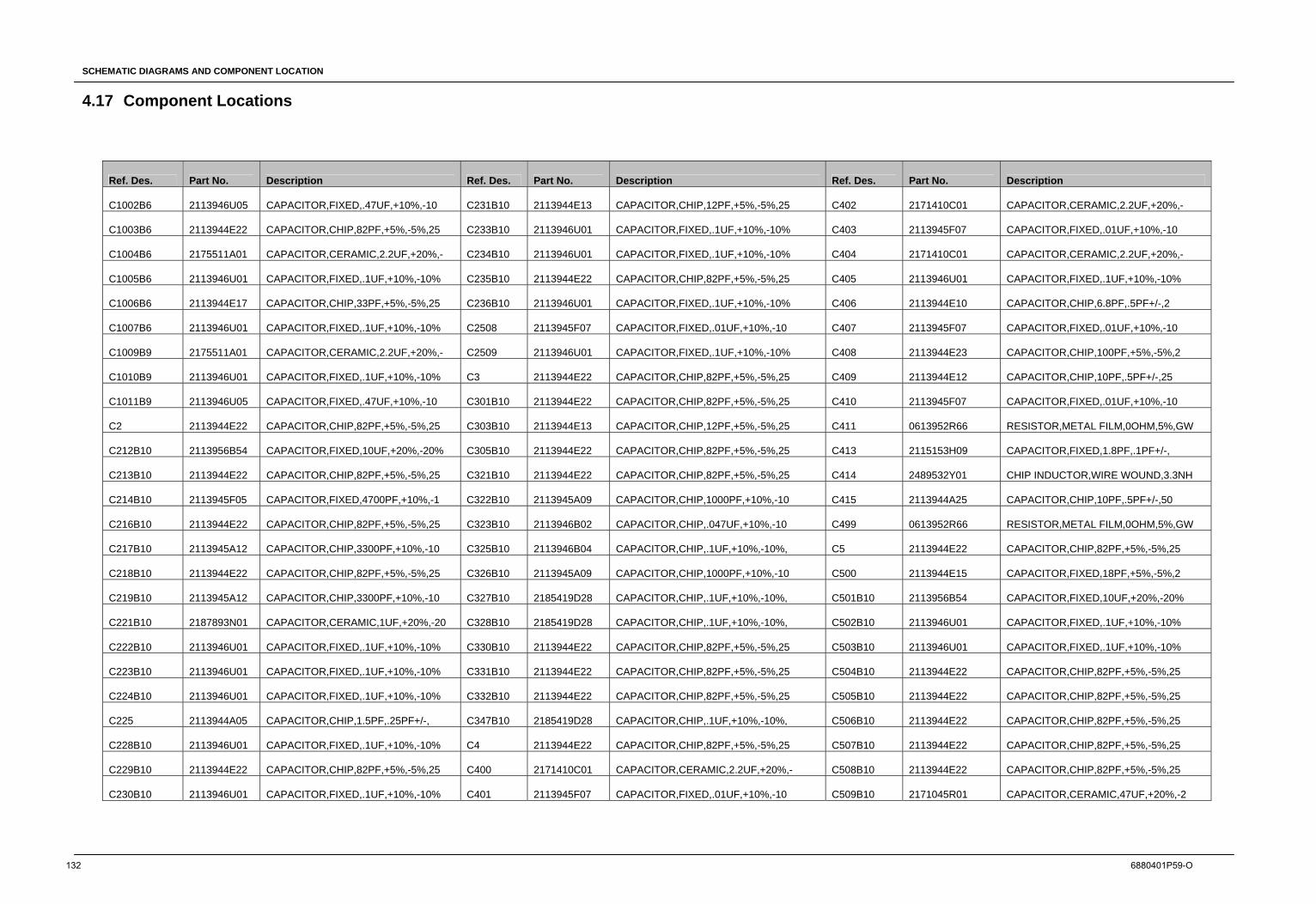
SCHEMATIC DIAGRAMS AND COMPONENT LOCATION
4.17 Component Locations
132 6880401P59-O
Ref. Des. Part No. Description Ref. Des. Part No. Description Ref. Des. Part No. Description
C1002B6 2113946U05 CAPACITOR,FIXED,.47UF,+10%,-10 C231B10 2113944E13 CAPACITOR,CHIP,12PF,+5%,-5%,25 C402 2171410C01 CAPACITOR,CERAMIC,2.2UF,+20%,-
C1003B6 2113944E22 CAPACITOR,CHIP,82PF,+5%,-5%,25 C233B10 2113946U01 CAPACITOR,FIXED,.1UF,+10%,-10% C403 2113945F07 CAPACITOR,FIXED,.01UF,+10%,-10
C1004B6 2175511A01 CAPACITOR,CERAMIC,2.2UF,+20%,- C234B10 2113946U01 CAPACITOR,FIXED,.1UF,+10%,-10% C404 2171410C01 CAPACITOR,CERAMIC,2.2UF,+20%,-
C1005B6 2113946U01 CAPACITOR,FIXED,.1UF,+10%,-10% C235B10 2113944E22 CAPACITOR,CHIP,82PF,+5%,-5%,25 C405 2113946U01 CAPACITOR,FIXED,.1UF,+10%,-10%
C1006B6 2113944E17 CAPACITOR,CHIP,33PF,+5%,-5%,25 C236B10 2113946U01 CAPACITOR,FIXED,.1UF,+10%,-10% C406 2113944E10 CAPACITOR,CHIP,6.8PF,.5PF+/-,2
C1007B6 2113946U01 CAPACITOR,FIXED,.1UF,+10%,-10% C2508 2113945F07 CAPACITOR,FIXED,.01UF,+10%,-10 C407 2113945F07 CAPACITOR,FIXED,.01UF,+10%,-10
C1009B9 2175511A01 CAPACITOR,CERAMIC,2.2UF,+20%,- C2509 2113946U01 CAPACITOR,FIXED,.1UF,+10%,-10% C408 2113944E23 CAPACITOR,CHIP,100PF,+5%,-5%,2
C1010B9 2113946U01 CAPACITOR,FIXED,.1UF,+10%,-10% C3 2113944E22 CAPACITOR,CHIP,82PF,+5%,-5%,25 C409 2113944E12 CAPACITOR,CHIP,10PF,.5PF+/-,25
C1011B9 2113946U05 CAPACITOR,FIXED,.47UF,+10%,-10 C301B10 2113944E22 CAPACITOR,CHIP,82PF,+5%,-5%,25 C410 2113945F07 CAPACITOR,FIXED,.01UF,+10%,-10
C2 2113944E22 CAPACITOR,CHIP,82PF,+5%,-5%,25 C303B10 2113944E13 CAPACITOR,CHIP,12PF,+5%,-5%,25 C411 0613952R66 RESISTOR,METAL FILM,0OHM,5%,GW
C212B10 2113956B54 CAPACITOR,FIXED,10UF,+20%,-20% C305B10 2113944E22 CAPACITOR,CHIP,82PF,+5%,-5%,25 C413 2115153H09 CAPACITOR,FIXED,1.8PF,.1PF+/-,
C213B10 2113944E22 CAPACITOR,CHIP,82PF,+5%,-5%,25 C321B10 2113944E22 CAPACITOR,CHIP,82PF,+5%,-5%,25 C414 2489532Y01 CHIP INDUCTOR,WIRE WOUND,3.3NH
C214B10 2113945F05 CAPACITOR,FIXED,4700PF,+10%,-1 C322B10 2113945A09 CAPACITOR,CHIP,1000PF,+10%,-10 C415 2113944A25 CAPACITOR,CHIP,10PF,.5PF+/-,50
C216B10 2113944E22 CAPACITOR,CHIP,82PF,+5%,-5%,25 C323B10 2113946B02 CAPACITOR,CHIP,.047UF,+10%,-10 C499 0613952R66 RESISTOR,METAL FILM,0OHM,5%,GW
C217B10 2113945A12 CAPACITOR,CHIP,3300PF,+10%,-10 C325B10 2113946B04 CAPACITOR,CHIP,.1UF,+10%,-10%, C5 2113944E22 CAPACITOR,CHIP,82PF,+5%,-5%,25
C218B10 2113944E22 CAPACITOR,CHIP,82PF,+5%,-5%,25 C326B10 2113945A09 CAPACITOR,CHIP,1000PF,+10%,-10 C500 2113944E15 CAPACITOR,FIXED,18PF,+5%,-5%,2
C219B10 2113945A12 CAPACITOR,CHIP,3300PF,+10%,-10 C327B10 2185419D28 CAPACITOR,CHIP,.1UF,+10%,-10%, C501B10 2113956B54 CAPACITOR,FIXED,10UF,+20%,-20%
C221B10 2187893N01 CAPACITOR,CERAMIC,1UF,+20%,-20 C328B10 2185419D28 CAPACITOR,CHIP,.1UF,+10%,-10%, C502B10 2113946U01 CAPACITOR,FIXED,.1UF,+10%,-10%
C222B10 2113946U01 CAPACITOR,FIXED,.1UF,+10%,-10% C330B10 2113944E22 CAPACITOR,CHIP,82PF,+5%,-5%,25 C503B10 2113946U01 CAPACITOR,FIXED,.1UF,+10%,-10%
C223B10 2113946U01 CAPACITOR,FIXED,.1UF,+10%,-10% C331B10 2113944E22 CAPACITOR,CHIP,82PF,+5%,-5%,25 C504B10 2113944E22 CAPACITOR,CHIP,82PF,+5%,-5%,25
C224B10 2113946U01 CAPACITOR,FIXED,.1UF,+10%,-10% C332B10 2113944E22 CAPACITOR,CHIP,82PF,+5%,-5%,25 C505B10 2113944E22 CAPACITOR,CHIP,82PF,+5%,-5%,25
C225 2113944A05 CAPACITOR,CHIP,1.5PF,.25PF+/-, C347B10 2185419D28 CAPACITOR,CHIP,.1UF,+10%,-10%, C506B10 2113944E22 CAPACITOR,CHIP,82PF,+5%,-5%,25
C228B10 2113946U01 CAPACITOR,FIXED,.1UF,+10%,-10% C4 2113944E22 CAPACITOR,CHIP,82PF,+5%,-5%,25 C507B10 2113944E22 CAPACITOR,CHIP,82PF,+5%,-5%,25
C229B10 2113944E22 CAPACITOR,CHIP,82PF,+5%,-5%,25 C400 2171410C01 CAPACITOR,CERAMIC,2.2UF,+20%,- C508B10 2113944E22 CAPACITOR,CHIP,82PF,+5%,-5%,25
C230B10 2113946U01 CAPACITOR,FIXED,.1UF,+10%,-10% C401 2113945F07 CAPACITOR,FIXED,.01UF,+10%,-10 C509B10 2171045R01 CAPACITOR,CERAMIC,47UF,+20%,-2
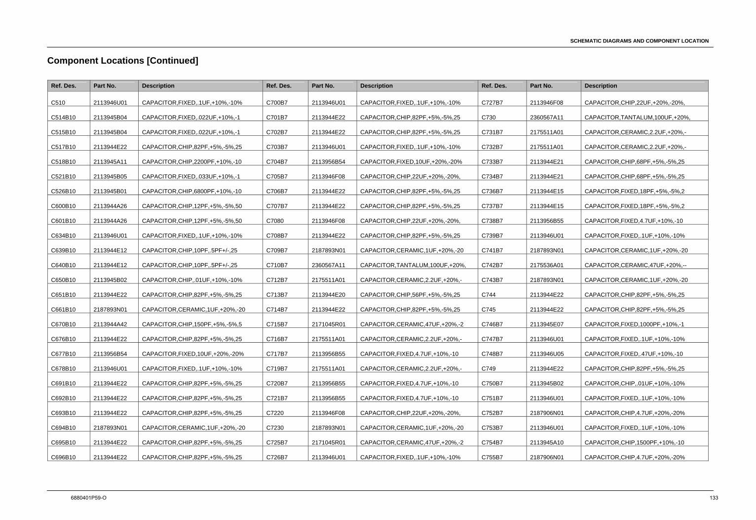
SCHEMATIC DIAGRAMS AND COMPONENT LOCATION
Component Locations [Continued]
6880401P59-O 133
Ref. Des. Part No. Description Ref. Des. Part No. Description Ref. Des. Part No. Description
C510 2113946U01 CAPACITOR,FIXED,.1UF,+10%,-10% C700B7 2113946U01 CAPACITOR,FIXED,.1UF,+10%,-10% C727B7 2113946F08 CAPACITOR,CHIP,22UF,+20%,-20%,
C514B10 2113945B04 CAPACITOR,FIXED,.022UF,+10%,-1 C701B7 2113944E22 CAPACITOR,CHIP,82PF,+5%,-5%,25 C730 2360567A11 CAPACITOR,TANTALUM,100UF,+20%,
C515B10 2113945B04 CAPACITOR,FIXED,.022UF,+10%,-1 C702B7 2113944E22 CAPACITOR,CHIP,82PF,+5%,-5%,25 C731B7 2175511A01 CAPACITOR,CERAMIC,2.2UF,+20%,-
C517B10 2113944E22 CAPACITOR,CHIP,82PF,+5%,-5%,25 C703B7 2113946U01 CAPACITOR,FIXED,.1UF,+10%,-10% C732B7 2175511A01 CAPACITOR,CERAMIC,2.2UF,+20%,-
C518B10 2113945A11 CAPACITOR,CHIP,2200PF,+10%,-10 C704B7 2113956B54 CAPACITOR,FIXED,10UF,+20%,-20% C733B7 2113944E21 CAPACITOR,CHIP,68PF,+5%,-5%,25
C521B10 2113945B05 CAPACITOR,FIXED,.033UF,+10%,-1 C705B7 2113946F08 CAPACITOR,CHIP,22UF,+20%,-20%, C734B7 2113944E21 CAPACITOR,CHIP,68PF,+5%,-5%,25
C526B10 2113945B01 CAPACITOR,CHIP,6800PF,+10%,-10 C706B7 2113944E22 CAPACITOR,CHIP,82PF,+5%,-5%,25 C736B7 2113944E15 CAPACITOR,FIXED,18PF,+5%,-5%,2
C600B10 2113944A26 CAPACITOR,CHIP,12PF,+5%,-5%,50 C707B7 2113944E22 CAPACITOR,CHIP,82PF,+5%,-5%,25 C737B7 2113944E15 CAPACITOR,FIXED,18PF,+5%,-5%,2
C601B10 2113944A26 CAPACITOR,CHIP,12PF,+5%,-5%,50 C7080 2113946F08 CAPACITOR,CHIP,22UF,+20%,-20%, C738B7 2113956B55 CAPACITOR,FIXED,4.7UF,+10%,-10
C634B10 2113946U01 CAPACITOR,FIXED,.1UF,+10%,-10% C708B7 2113944E22 CAPACITOR,CHIP,82PF,+5%,-5%,25 C739B7 2113946U01 CAPACITOR,FIXED,.1UF,+10%,-10%
C639B10 2113944E12 CAPACITOR,CHIP,10PF,.5PF+/-,25 C709B7 2187893N01 CAPACITOR,CERAMIC,1UF,+20%,-20 C741B7 2187893N01 CAPACITOR,CERAMIC,1UF,+20%,-20
C640B10 2113944E12 CAPACITOR,CHIP,10PF,.5PF+/-,25 C710B7 2360567A11 CAPACITOR,TANTALUM,100UF,+20%, C742B7 2175536A01 CAPACITOR,CERAMIC,47UF,+20%,--
C650B10 2113945B02 CAPACITOR,CHIP,.01UF,+10%,-10% C712B7 2175511A01 CAPACITOR,CERAMIC,2.2UF,+20%,- C743B7 2187893N01 CAPACITOR,CERAMIC,1UF,+20%,-20
C651B10 2113944E22 CAPACITOR,CHIP,82PF,+5%,-5%,25 C713B7 2113944E20 CAPACITOR,CHIP,56PF,+5%,-5%,25 C744 2113944E22 CAPACITOR,CHIP,82PF,+5%,-5%,25
C661B10 2187893N01 CAPACITOR,CERAMIC,1UF,+20%,-20 C714B7 2113944E22 CAPACITOR,CHIP,82PF,+5%,-5%,25 C745 2113944E22 CAPACITOR,CHIP,82PF,+5%,-5%,25
C670B10 2113944A42 CAPACITOR,CHIP,150PF,+5%,-5%,5 C715B7 2171045R01 CAPACITOR,CERAMIC,47UF,+20%,-2 C746B7 2113945E07 CAPACITOR,FIXED,1000PF,+10%,-1
C676B10 2113944E22 CAPACITOR,CHIP,82PF,+5%,-5%,25 C716B7 2175511A01 CAPACITOR,CERAMIC,2.2UF,+20%,- C747B7 2113946U01 CAPACITOR,FIXED,.1UF,+10%,-10%
C677B10 2113956B54 CAPACITOR,FIXED,10UF,+20%,-20% C717B7 2113956B55 CAPACITOR,FIXED,4.7UF,+10%,-10 C748B7 2113946U05 CAPACITOR,FIXED,.47UF,+10%,-10
C678B10 2113946U01 CAPACITOR,FIXED,.1UF,+10%,-10% C719B7 2175511A01 CAPACITOR,CERAMIC,2.2UF,+20%,- C749 2113944E22 CAPACITOR,CHIP,82PF,+5%,-5%,25
C691B10 2113944E22 CAPACITOR,CHIP,82PF,+5%,-5%,25 C720B7 2113956B55 CAPACITOR,FIXED,4.7UF,+10%,-10 C750B7 2113945B02 CAPACITOR,CHIP,.01UF,+10%,-10%
C692B10 2113944E22 CAPACITOR,CHIP,82PF,+5%,-5%,25 C721B7 2113956B55 CAPACITOR,FIXED,4.7UF,+10%,-10 C751B7 2113946U01 CAPACITOR,FIXED,.1UF,+10%,-10%
C693B10 2113944E22 CAPACITOR,CHIP,82PF,+5%,-5%,25 C7220 2113946F08 CAPACITOR,CHIP,22UF,+20%,-20%, C752B7 2187906N01 CAPACITOR,CHIP,4.7UF,+20%,-20%
C694B10 2187893N01 CAPACITOR,CERAMIC,1UF,+20%,-20 C7230 2187893N01 CAPACITOR,CERAMIC,1UF,+20%,-20 C753B7 2113946U01 CAPACITOR,FIXED,.1UF,+10%,-10%
C695B10 2113944E22 CAPACITOR,CHIP,82PF,+5%,-5%,25 C725B7 2171045R01 CAPACITOR,CERAMIC,47UF,+20%,-2 C754B7 2113945A10 CAPACITOR,CHIP,1500PF,+10%,-10
C696B10 2113944E22 CAPACITOR,CHIP,82PF,+5%,-5%,25 C726B7 2113946U01 CAPACITOR,FIXED,.1UF,+10%,-10% C755B7 2187906N01 CAPACITOR,CHIP,4.7UF,+20%,-20%
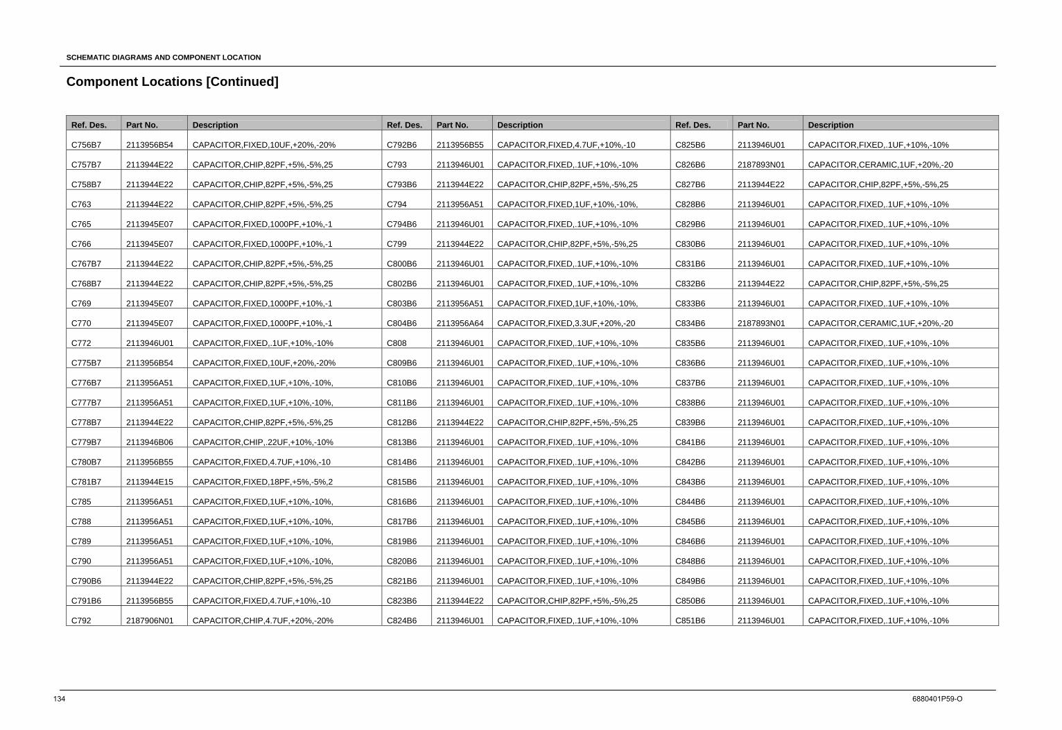
SCHEMATIC DIAGRAMS AND COMPONENT LOCATION
Component Locations [Continued]
134 6880401P59-O
Ref. Des. Part No. Description Ref. Des. Part No. Description Ref. Des. Part No. Description
C756B7 2113956B54 CAPACITOR,FIXED,10UF,+20%,-20% C792B6 2113956B55 CAPACITOR,FIXED,4.7UF,+10%,-10 C825B6 2113946U01 CAPACITOR,FIXED,.1UF,+10%,-10%
C757B7 2113944E22 CAPACITOR,CHIP,82PF,+5%,-5%,25 C793 2113946U01 CAPACITOR,FIXED,.1UF,+10%,-10% C826B6 2187893N01 CAPACITOR,CERAMIC,1UF,+20%,-20
C758B7 2113944E22 CAPACITOR,CHIP,82PF,+5%,-5%,25 C793B6 2113944E22 CAPACITOR,CHIP,82PF,+5%,-5%,25 C827B6 2113944E22 CAPACITOR,CHIP,82PF,+5%,-5%,25
C763 2113944E22 CAPACITOR,CHIP,82PF,+5%,-5%,25 C794 2113956A51 CAPACITOR,FIXED,1UF,+10%,-10%, C828B6 2113946U01 CAPACITOR,FIXED,.1UF,+10%,-10%
C765 2113945E07 CAPACITOR,FIXED,1000PF,+10%,-1 C794B6 2113946U01 CAPACITOR,FIXED,.1UF,+10%,-10% C829B6 2113946U01 CAPACITOR,FIXED,.1UF,+10%,-10%
C766 2113945E07 CAPACITOR,FIXED,1000PF,+10%,-1 C799 2113944E22 CAPACITOR,CHIP,82PF,+5%,-5%,25 C830B6 2113946U01 CAPACITOR,FIXED,.1UF,+10%,-10%
C767B7 2113944E22 CAPACITOR,CHIP,82PF,+5%,-5%,25 C800B6 2113946U01 CAPACITOR,FIXED,.1UF,+10%,-10% C831B6 2113946U01 CAPACITOR,FIXED,.1UF,+10%,-10%
C768B7 2113944E22 CAPACITOR,CHIP,82PF,+5%,-5%,25 C802B6 2113946U01 CAPACITOR,FIXED,.1UF,+10%,-10% C832B6 2113944E22 CAPACITOR,CHIP,82PF,+5%,-5%,25
C769 2113945E07 CAPACITOR,FIXED,1000PF,+10%,-1 C803B6 2113956A51 CAPACITOR,FIXED,1UF,+10%,-10%, C833B6 2113946U01 CAPACITOR,FIXED,.1UF,+10%,-10%
C770 2113945E07 CAPACITOR,FIXED,1000PF,+10%,-1 C804B6 2113956A64 CAPACITOR,FIXED,3.3UF,+20%,-20 C834B6 2187893N01 CAPACITOR,CERAMIC,1UF,+20%,-20
C772 2113946U01 CAPACITOR,FIXED,.1UF,+10%,-10% C808 2113946U01 CAPACITOR,FIXED,.1UF,+10%,-10% C835B6 2113946U01 CAPACITOR,FIXED,.1UF,+10%,-10%
C775B7 2113956B54 CAPACITOR,FIXED,10UF,+20%,-20% C809B6 2113946U01 CAPACITOR,FIXED,.1UF,+10%,-10% C836B6 2113946U01 CAPACITOR,FIXED,.1UF,+10%,-10%
C776B7 2113956A51 CAPACITOR,FIXED,1UF,+10%,-10%, C810B6 2113946U01 CAPACITOR,FIXED,.1UF,+10%,-10% C837B6 2113946U01 CAPACITOR,FIXED,.1UF,+10%,-10%
C777B7 2113956A51 CAPACITOR,FIXED,1UF,+10%,-10%, C811B6 2113946U01 CAPACITOR,FIXED,.1UF,+10%,-10% C838B6 2113946U01 CAPACITOR,FIXED,.1UF,+10%,-10%
C778B7 2113944E22 CAPACITOR,CHIP,82PF,+5%,-5%,25 C812B6 2113944E22 CAPACITOR,CHIP,82PF,+5%,-5%,25 C839B6 2113946U01 CAPACITOR,FIXED,.1UF,+10%,-10%
C779B7 2113946B06 CAPACITOR,CHIP,.22UF,+10%,-10% C813B6 2113946U01 CAPACITOR,FIXED,.1UF,+10%,-10% C841B6 2113946U01 CAPACITOR,FIXED,.1UF,+10%,-10%
C780B7 2113956B55 CAPACITOR,FIXED,4.7UF,+10%,-10 C814B6 2113946U01 CAPACITOR,FIXED,.1UF,+10%,-10% C842B6 2113946U01 CAPACITOR,FIXED,.1UF,+10%,-10%
C781B7 2113944E15 CAPACITOR,FIXED,18PF,+5%,-5%,2 C815B6 2113946U01 CAPACITOR,FIXED,.1UF,+10%,-10% C843B6 2113946U01 CAPACITOR,FIXED,.1UF,+10%,-10%
C785 2113956A51 CAPACITOR,FIXED,1UF,+10%,-10%, C816B6 2113946U01 CAPACITOR,FIXED,.1UF,+10%,-10% C844B6 2113946U01 CAPACITOR,FIXED,.1UF,+10%,-10%
C788 2113956A51 CAPACITOR,FIXED,1UF,+10%,-10%, C817B6 2113946U01 CAPACITOR,FIXED,.1UF,+10%,-10% C845B6 2113946U01 CAPACITOR,FIXED,.1UF,+10%,-10%
C789 2113956A51 CAPACITOR,FIXED,1UF,+10%,-10%, C819B6 2113946U01 CAPACITOR,FIXED,.1UF,+10%,-10% C846B6 2113946U01 CAPACITOR,FIXED,.1UF,+10%,-10%
C790 2113956A51 CAPACITOR,FIXED,1UF,+10%,-10%, C820B6 2113946U01 CAPACITOR,FIXED,.1UF,+10%,-10% C848B6 2113946U01 CAPACITOR,FIXED,.1UF,+10%,-10%
C790B6 2113944E22 CAPACITOR,CHIP,82PF,+5%,-5%,25 C821B6 2113946U01 CAPACITOR,FIXED,.1UF,+10%,-10% C849B6 2113946U01 CAPACITOR,FIXED,.1UF,+10%,-10%
C791B6 2113956B55 CAPACITOR,FIXED,4.7UF,+10%,-10 C823B6 2113944E22 CAPACITOR,CHIP,82PF,+5%,-5%,25 C850B6 2113946U01 CAPACITOR,FIXED,.1UF,+10%,-10%
C792 2187906N01 CAPACITOR,CHIP,4.7UF,+20%,-20% C824B6 2113946U01 CAPACITOR,FIXED,.1UF,+10%,-10% C851B6 2113946U01 CAPACITOR,FIXED,.1UF,+10%,-10%
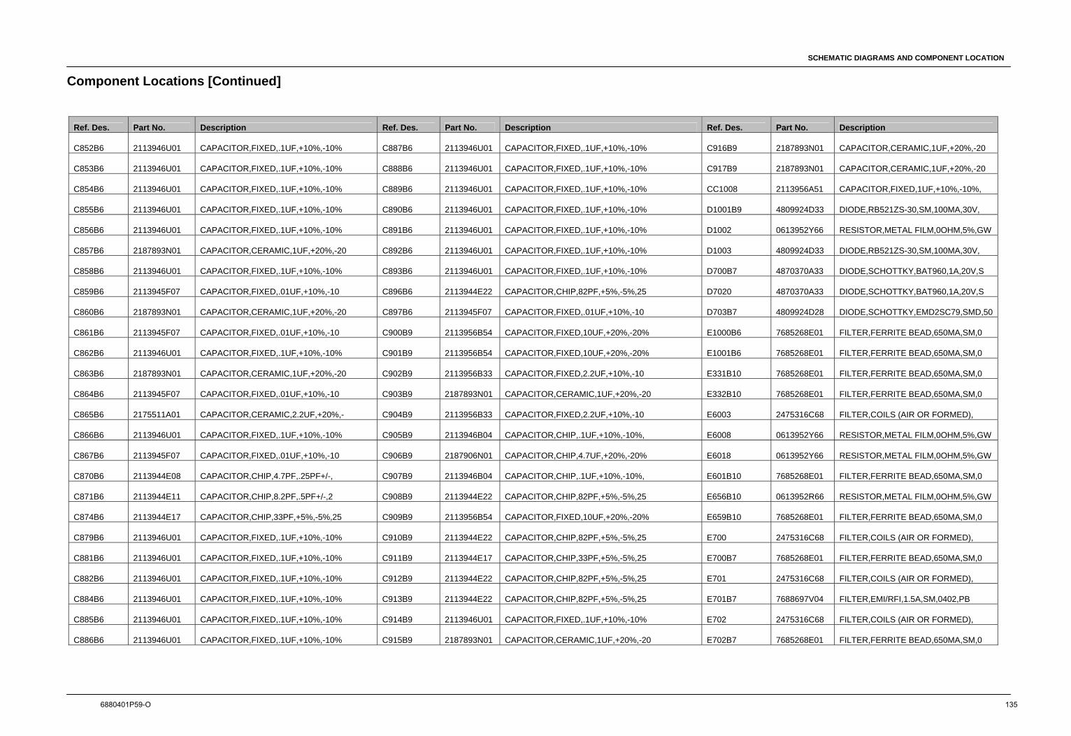
SCHEMATIC DIAGRAMS AND COMPONENT LOCATION
Component Locations [Continued]
6880401P59-O 135
Ref. Des. Part No. Description Ref. Des. Part No. Description Ref. Des. Part No. Description
C852B6 2113946U01 CAPACITOR,FIXED,.1UF,+10%,-10% C887B6 2113946U01 CAPACITOR,FIXED,.1UF,+10%,-10% C916B9 2187893N01 CAPACITOR,CERAMIC,1UF,+20%,-20
C853B6 2113946U01 CAPACITOR,FIXED,.1UF,+10%,-10% C888B6 2113946U01 CAPACITOR,FIXED,.1UF,+10%,-10% C917B9 2187893N01 CAPACITOR,CERAMIC,1UF,+20%,-20
C854B6 2113946U01 CAPACITOR,FIXED,.1UF,+10%,-10% C889B6 2113946U01 CAPACITOR,FIXED,.1UF,+10%,-10% CC1008 2113956A51 CAPACITOR,FIXED,1UF,+10%,-10%,
C855B6 2113946U01 CAPACITOR,FIXED,.1UF,+10%,-10% C890B6 2113946U01 CAPACITOR,FIXED,.1UF,+10%,-10% D1001B9 4809924D33 DIODE,RB521ZS-30,SM,100MA,30V,
C856B6 2113946U01 CAPACITOR,FIXED,.1UF,+10%,-10% C891B6 2113946U01 CAPACITOR,FIXED,.1UF,+10%,-10% D1002 0613952Y66 RESISTOR,METAL FILM,0OHM,5%,GW
C857B6 2187893N01 CAPACITOR,CERAMIC,1UF,+20%,-20 C892B6 2113946U01 CAPACITOR,FIXED,.1UF,+10%,-10% D1003 4809924D33 DIODE,RB521ZS-30,SM,100MA,30V,
C858B6 2113946U01 CAPACITOR,FIXED,.1UF,+10%,-10% C893B6 2113946U01 CAPACITOR,FIXED,.1UF,+10%,-10% D700B7 4870370A33 DIODE,SCHOTTKY,BAT960,1A,20V,S
C859B6 2113945F07 CAPACITOR,FIXED,.01UF,+10%,-10 C896B6 2113944E22 CAPACITOR,CHIP,82PF,+5%,-5%,25 D7020 4870370A33 DIODE,SCHOTTKY,BAT960,1A,20V,S
C860B6 2187893N01 CAPACITOR,CERAMIC,1UF,+20%,-20 C897B6 2113945F07 CAPACITOR,FIXED,.01UF,+10%,-10 D703B7 4809924D28 DIODE,SCHOTTKY,EMD2SC79,SMD,50
C861B6 2113945F07 CAPACITOR,FIXED,.01UF,+10%,-10 C900B9 2113956B54 CAPACITOR,FIXED,10UF,+20%,-20% E1000B6 7685268E01 FILTER,FERRITE BEAD,650MA,SM,0
C862B6 2113946U01 CAPACITOR,FIXED,.1UF,+10%,-10% C901B9 2113956B54 CAPACITOR,FIXED,10UF,+20%,-20% E1001B6 7685268E01 FILTER,FERRITE BEAD,650MA,SM,0
C863B6 2187893N01 CAPACITOR,CERAMIC,1UF,+20%,-20 C902B9 2113956B33 CAPACITOR,FIXED,2.2UF,+10%,-10 E331B10 7685268E01 FILTER,FERRITE BEAD,650MA,SM,0
C864B6 2113945F07 CAPACITOR,FIXED,.01UF,+10%,-10 C903B9 2187893N01 CAPACITOR,CERAMIC,1UF,+20%,-20 E332B10 7685268E01 FILTER,FERRITE BEAD,650MA,SM,0
C865B6 2175511A01 CAPACITOR,CERAMIC,2.2UF,+20%,- C904B9 2113956B33 CAPACITOR,FIXED,2.2UF,+10%,-10 E6003 2475316C68 FILTER,COILS (AIR OR FORMED),
C866B6 2113946U01 CAPACITOR,FIXED,.1UF,+10%,-10% C905B9 2113946B04 CAPACITOR,CHIP,.1UF,+10%,-10%, E6008 0613952Y66 RESISTOR,METAL FILM,0OHM,5%,GW
C867B6 2113945F07 CAPACITOR,FIXED,.01UF,+10%,-10 C906B9 2187906N01 CAPACITOR,CHIP,4.7UF,+20%,-20% E6018 0613952Y66 RESISTOR,METAL FILM,0OHM,5%,GW
C870B6 2113944E08 CAPACITOR,CHIP,4.7PF,.25PF+/-, C907B9 2113946B04 CAPACITOR,CHIP,.1UF,+10%,-10%, E601B10 7685268E01 FILTER,FERRITE BEAD,650MA,SM,0
C871B6 2113944E11 CAPACITOR,CHIP,8.2PF,.5PF+/-,2 C908B9 2113944E22 CAPACITOR,CHIP,82PF,+5%,-5%,25 E656B10 0613952R66 RESISTOR,METAL FILM,0OHM,5%,GW
C874B6 2113944E17 CAPACITOR,CHIP,33PF,+5%,-5%,25 C909B9 2113956B54 CAPACITOR,FIXED,10UF,+20%,-20% E659B10 7685268E01 FILTER,FERRITE BEAD,650MA,SM,0
C879B6 2113946U01 CAPACITOR,FIXED,.1UF,+10%,-10% C910B9 2113944E22 CAPACITOR,CHIP,82PF,+5%,-5%,25 E700 2475316C68 FILTER,COILS (AIR OR FORMED),
C881B6 2113946U01 CAPACITOR,FIXED,.1UF,+10%,-10% C911B9 2113944E17 CAPACITOR,CHIP,33PF,+5%,-5%,25 E700B7 7685268E01 FILTER,FERRITE BEAD,650MA,SM,0
C882B6 2113946U01 CAPACITOR,FIXED,.1UF,+10%,-10% C912B9 2113944E22 CAPACITOR,CHIP,82PF,+5%,-5%,25 E701 2475316C68 FILTER,COILS (AIR OR FORMED),
C884B6 2113946U01 CAPACITOR,FIXED,.1UF,+10%,-10% C913B9 2113944E22 CAPACITOR,CHIP,82PF,+5%,-5%,25 E701B7 7688697V04 FILTER,EMI/RFI,1.5A,SM,0402,PB
C885B6 2113946U01 CAPACITOR,FIXED,.1UF,+10%,-10% C914B9 2113946U01 CAPACITOR,FIXED,.1UF,+10%,-10% E702 2475316C68 FILTER,COILS (AIR OR FORMED),
C886B6 2113946U01 CAPACITOR,FIXED,.1UF,+10%,-10% C915B9 2187893N01 CAPACITOR,CERAMIC,1UF,+20%,-20 E702B7 7685268E01 FILTER,FERRITE BEAD,650MA,SM,0
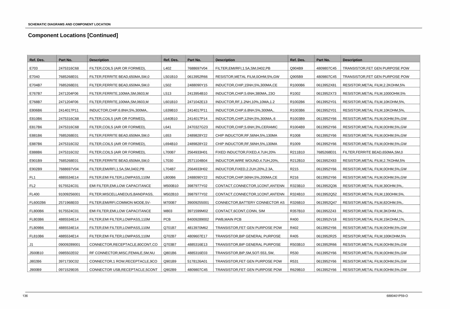
SCHEMATIC DIAGRAMS AND COMPONENT LOCATION
Component Locations [Continued]
136 6880401P59-O
Ref. Des. Part No. Description Ref. Des. Part No. Description Ref. Des. Part No. Description
E703 2475316C68 FILTER,COILS (AIR OR FORMED), L402 7688697V04 FILTER,EMI/RFI,1.5A,SM,0402,PB Q904B9 4809807C45 TRANSISTOR,FET GEN PURPOSE POW
E7040 7685268E01 FILTER,FERRITE BEAD,650MA,SM,0 L501B10 0613952R66 RESISTOR,METAL FILM,0OHM,5%,GW Q905B9 4809807C45 TRANSISTOR,FET GEN PURPOSE POW
E704B7 7685268E01 FILTER,FERRITE BEAD,650MA,SM,0 L502 2488090Y15 INDUCTOR,CHIP,15NH,5%,300MA,CE R1000B6 0613952X81 RESISTOR,METAL FILM,2.2KOHM,5%
E767B7 2471204F06 FILTER,FERRITE,100MA,SM,0603,M L513 2413954B10 INDUCTOR,CHIP,5.6NH,380MA,.23O R1002 0613952X73 RESISTOR,METAL FILM,1000OHM,5%
E768B7 2471204F06 FILTER,FERRITE,100MA,SM,0603,M L601B10 2471042E13 INDUCTOR,RF,1.2NH,10%,10MA,1.2 R1002B6 0613952Y01 RESISTOR,METAL FILM,10KOHM,5%,
E806B6 2414017P11 INDUCTOR,CHIP,6.8NH,5%,300MA,. L639B10 2414017P11 INDUCTOR,CHIP,6.8NH,5%,300MA,. R1003B6 0613952Y01 RESISTOR,METAL FILM,10KOHM,5%,
E810B6 2475316C68 FILTER,COILS (AIR OR FORMED), L640B10 2414017P14 INDUCTOR,CHIP,12NH,5%,300MA,.6 R1003B9 0613952Y66 RESISTOR,METAL FILM,0OHM,5%,GW
E817B6 2475316C68 FILTER,COILS (AIR OR FORMED), L641 2470327G23 INDUCTOR,CHIP,5.6NH,3%,CERAMIC R1004B9 0613952Y66 RESISTOR,METAL FILM,0OHM,5%,GW
E881B6 7685268E01 FILTER,FERRITE BEAD,650MA,SM,0 L653 2489828Y22 CHIP INDUCTOR,RF,56NH,5%,130MA R1008 0613952Y66 RESISTOR,METAL FILM,0OHM,5%,GW
E887B6 2475316C02 FILTER,COILS (AIR OR FORMED), L694B10 2489828Y22 CHIP INDUCTOR,RF,56NH,5%,130MA R1009 0613952Y66 RESISTOR,METAL FILM,0OHM,5%,GW
E888B6 2475316C02 FILTER,COILS (AIR OR FORMED), L700B7 2564933H01 FIXED INDUCTOR,FIXED,4.7UH,20% R211B10 7685268E01 FILTER,FERRITE BEAD,650MA,SM,0
E901B9 7685268E01 FILTER,FERRITE BEAD,650MA,SM,0 L7030 2571104B04 INDUCTOR,WIRE WOUND,4.7UH,20%, R212B10 0613952X83 RESISTOR,METAL FILM,2.7KOHM,5%
E902B9 7688697V04 FILTER,EMI/RFI,1.5A,SM,0402,PB L704B7 2564933H02 INDUCTOR,FIXED,2.2UH,20%,2.3A, R215 0613952Y66 RESISTOR,METAL FILM,0OHM,5%,GW
FL1 4885534E14 FILTER,EMI FILTER,LOWPASS,110M L800B6 2488090Y22 INDUCTOR,CHIP,56NH,5%,200MA,CE R216 0613952Y66 RESISTOR,METAL FILM,0OHM,5%,GW
FL2 9175524C01 EMI FILTER,EMI,LOW CAPACITANCE M500B10 3987977Y02 CONTACT,CONNECTOR,1CONT,ANTENN R323B10 0613952Q36 RESISTOR,METAL FILM,30OHM,5%,.
FL400 91009256001 FILTER,MISCELLANEOUS,BANDPASS, M502B10 3987977Y02 CONTACT,CONNECTOR,1CONT,ANTENN R324B10 0613952Q52 RESISTOR,METAL FILM,130OHM,5%,
FL6002B6 2571968E03 FILTER,EMI/RFI,COMMON MODE,5V- M700B7 39009255001 CONNECTOR,BATTERY CONNECTOR AS R326B10 0613952Q47 RESISTOR,METAL FILM,82OHM,5%,.
FL800B6 9175524C01 EMI FILTER,EMI,LOW CAPACITANCE M803 3971599M02 CONTACT,6CONT,CONN, SIM R357B10 0613952Z43 RESISTOR,METAL FILM,3KOHM,1%,.
FL803B6 4885534E14 FILTER,EMI FILTER,LOWPASS,110M PCB 84009289002 PWB,MAIN PCB R400 0613952V18 RESISTOR,METAL FILM,15KOHM,1%,
FL809B6 4885534E14 FILTER,EMI FILTER,LOWPASS,110M Q701B7 4813970M62 TRANSISTOR,FET GEN PURPOSE POW R402 0613952Y66 RESISTOR,METAL FILM,0OHM,5%,GW
FL810B6 4885534E14 FILTER,EMI FILTER,LOWPASS,110M Q702B7 4809607E17 TRANSISTOR,BIP GENERAL PURPOSE R405 0613952R25 RESISTOR,METAL FILM,100KOHM,5%
J1 09009289001 CONNECTOR,RECEPTACLE,80CONT,CO Q703B7 4885316E13 TRANSISTOR,BIP GENERAL PURPOSE R503B10 0613952R66 RESISTOR,METAL FILM,0OHM,5%,GW
J500B10 0985502E02 RF CONNECTOR,MISC,FEMALE,SM,NU Q801B6 4885316E03 TRANSISTOR,BIP,SM,SOT-553,.5W, R530 0613952Y66 RESISTOR,METAL FILM,0OHM,5%,GW
J802B6 3971730C02 CONNECTOR,1 ROW,RECEPTACLE,9CO Q901B9 5178126A01 TRANSISTOR,FET GEN PURPOSE POW R531 0613952Y66 RESISTOR,METAL FILM,0OHM,5%,GW
J900B9 0971529E05 CONNECTOR USB,RECEPTACLE,5CONT Q902B9 4809807C45 TRANSISTOR,FET GEN PURPOSE POW R629B10 0613952Y66 RESISTOR,METAL FILM,0OHM,5%,GW
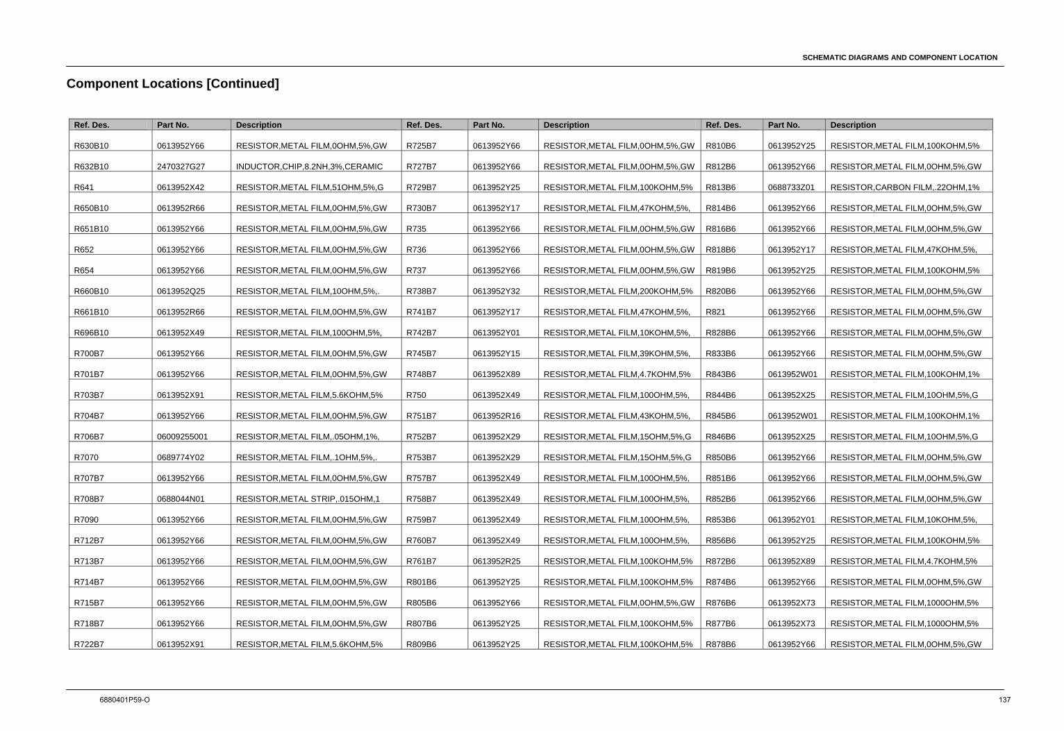
SCHEMATIC DIAGRAMS AND COMPONENT LOCATION
Component Locations [Continued]
6880401P59-O 137
Ref. Des. Part No. Description Ref. Des. Part No. Description Ref. Des. Part No. Description
R630B10 0613952Y66 RESISTOR,METAL FILM,0OHM,5%,GW R725B7 0613952Y66 RESISTOR,METAL FILM,0OHM,5%,GW R810B6 0613952Y25 RESISTOR,METAL FILM,100KOHM,5%
R632B10 2470327G27 INDUCTOR,CHIP,8.2NH,3%,CERAMIC R727B7 0613952Y66 RESISTOR,METAL FILM,0OHM,5%,GW R812B6 0613952Y66 RESISTOR,METAL FILM,0OHM,5%,GW
R641 0613952X42 RESISTOR,METAL FILM,51OHM,5%,G R729B7 0613952Y25 RESISTOR,METAL FILM,100KOHM,5% R813B6 0688733Z01 RESISTOR,CARBON FILM,.22OHM,1%
R650B10 0613952R66 RESISTOR,METAL FILM,0OHM,5%,GW R730B7 0613952Y17 RESISTOR,METAL FILM,47KOHM,5%, R814B6 0613952Y66 RESISTOR,METAL FILM,0OHM,5%,GW
R651B10 0613952Y66 RESISTOR,METAL FILM,0OHM,5%,GW R735 0613952Y66 RESISTOR,METAL FILM,0OHM,5%,GW R816B6 0613952Y66 RESISTOR,METAL FILM,0OHM,5%,GW
R652 0613952Y66 RESISTOR,METAL FILM,0OHM,5%,GW R736 0613952Y66 RESISTOR,METAL FILM,0OHM,5%,GW R818B6 0613952Y17 RESISTOR,METAL FILM,47KOHM,5%,
R654 0613952Y66 RESISTOR,METAL FILM,0OHM,5%,GW R737 0613952Y66 RESISTOR,METAL FILM,0OHM,5%,GW R819B6 0613952Y25 RESISTOR,METAL FILM,100KOHM,5%
R660B10 0613952Q25 RESISTOR,METAL FILM,10OHM,5%,. R738B7 0613952Y32 RESISTOR,METAL FILM,200KOHM,5% R820B6 0613952Y66 RESISTOR,METAL FILM,0OHM,5%,GW
R661B10 0613952R66 RESISTOR,METAL FILM,0OHM,5%,GW R741B7 0613952Y17 RESISTOR,METAL FILM,47KOHM,5%, R821 0613952Y66 RESISTOR,METAL FILM,0OHM,5%,GW
R696B10 0613952X49 RESISTOR,METAL FILM,100OHM,5%, R742B7 0613952Y01 RESISTOR,METAL FILM,10KOHM,5%, R828B6 0613952Y66 RESISTOR,METAL FILM,0OHM,5%,GW
R700B7 0613952Y66 RESISTOR,METAL FILM,0OHM,5%,GW R745B7 0613952Y15 RESISTOR,METAL FILM,39KOHM,5%, R833B6 0613952Y66 RESISTOR,METAL FILM,0OHM,5%,GW
R701B7 0613952Y66 RESISTOR,METAL FILM,0OHM,5%,GW R748B7 0613952X89 RESISTOR,METAL FILM,4.7KOHM,5% R843B6 0613952W01 RESISTOR,METAL FILM,100KOHM,1%
R703B7 0613952X91 RESISTOR,METAL FILM,5.6KOHM,5% R750 0613952X49 RESISTOR,METAL FILM,100OHM,5%, R844B6 0613952X25 RESISTOR,METAL FILM,10OHM,5%,G
R704B7 0613952Y66 RESISTOR,METAL FILM,0OHM,5%,GW R751B7 0613952R16 RESISTOR,METAL FILM,43KOHM,5%, R845B6 0613952W01 RESISTOR,METAL FILM,100KOHM,1%
R706B7 06009255001 RESISTOR,METAL FILM,.05OHM,1%, R752B7 0613952X29 RESISTOR,METAL FILM,15OHM,5%,G R846B6 0613952X25 RESISTOR,METAL FILM,10OHM,5%,G
R7070 0689774Y02 RESISTOR,METAL FILM,.1OHM,5%,. R753B7 0613952X29 RESISTOR,METAL FILM,15OHM,5%,G R850B6 0613952Y66 RESISTOR,METAL FILM,0OHM,5%,GW
R707B7 0613952Y66 RESISTOR,METAL FILM,0OHM,5%,GW R757B7 0613952X49 RESISTOR,METAL FILM,100OHM,5%, R851B6 0613952Y66 RESISTOR,METAL FILM,0OHM,5%,GW
R708B7 0688044N01 RESISTOR,METAL STRIP,.015OHM,1 R758B7 0613952X49 RESISTOR,METAL FILM,100OHM,5%, R852B6 0613952Y66 RESISTOR,METAL FILM,0OHM,5%,GW
R7090 0613952Y66 RESISTOR,METAL FILM,0OHM,5%,GW R759B7 0613952X49 RESISTOR,METAL FILM,100OHM,5%, R853B6 0613952Y01 RESISTOR,METAL FILM,10KOHM,5%,
R712B7 0613952Y66 RESISTOR,METAL FILM,0OHM,5%,GW R760B7 0613952X49 RESISTOR,METAL FILM,100OHM,5%, R856B6 0613952Y25 RESISTOR,METAL FILM,100KOHM,5%
R713B7 0613952Y66 RESISTOR,METAL FILM,0OHM,5%,GW R761B7 0613952R25 RESISTOR,METAL FILM,100KOHM,5% R872B6 0613952X89 RESISTOR,METAL FILM,4.7KOHM,5%
R714B7 0613952Y66 RESISTOR,METAL FILM,0OHM,5%,GW R801B6 0613952Y25 RESISTOR,METAL FILM,100KOHM,5% R874B6 0613952Y66 RESISTOR,METAL FILM,0OHM,5%,GW
R715B7 0613952Y66 RESISTOR,METAL FILM,0OHM,5%,GW R805B6 0613952Y66 RESISTOR,METAL FILM,0OHM,5%,GW R876B6 0613952X73 RESISTOR,METAL FILM,1000OHM,5%
R718B7 0613952Y66 RESISTOR,METAL FILM,0OHM,5%,GW R807B6 0613952Y25 RESISTOR,METAL FILM,100KOHM,5% R877B6 0613952X73 RESISTOR,METAL FILM,1000OHM,5%
R722B7 0613952X91 RESISTOR,METAL FILM,5.6KOHM,5% R809B6 0613952Y25 RESISTOR,METAL FILM,100KOHM,5% R878B6 0613952Y66 RESISTOR,METAL FILM,0OHM,5%,GW
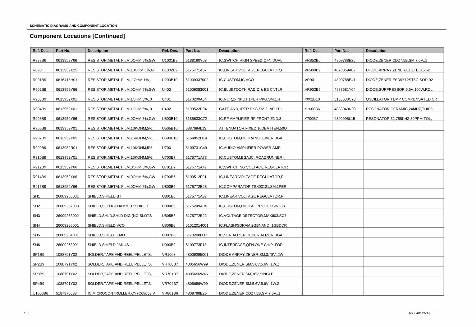
SCHEMATIC DIAGRAMS AND COMPONENT LOCATION
Component Locations [Continued]
138 6880401P59-O
Ref. Des. Part No. Description Ref. Des. Part No. Description Ref. Des. Part No. Description
R888B6 0613952Y66 RESISTOR,METAL FILM,0OHM,5%,GW U1001B9 5188160Y03 IC,SWITCH,HIGH SPEED,QFN,DUAL VR852B6 4809788E25 DIODE,ZENER,CDZ7.5B,SM,7.6V,.1
R890 0613952X25 RESISTOR,METAL FILM,10OHM,5%,G U1002B9 5175771A37 IC,LINEAR VOLTAGE REGULATOR,FI VR900B9 4870359A02 DIODE ARRAY,ZENER,EDZTE615.6B,
R901B9 0616416H01 RESISTOR,METAL FILM,.1OHM,1%,. U200B10 51009337002 IC,CUSTOM,IC VCO VR901 4809788E41 DIODE,ZENER,ESD9X12ST5G,SOD-92
R902B9 0613952Y66 RESISTOR,METAL FILM,0OHM,5%,GW U400 51009283001 IC,BLUETOOTH RADIO & BB CNTLR, VR902B9 4888581Y04 DIODE,SUPPRESSOR,5.5V,100W,RCL
R903B9 0613952X01 RESISTOR,METAL FILM,1OHM,5%,.0 U401 5170200A64 IC,NOR,2-INPUT,1PER PKG,SM,1.4 Y002B10 5185633C78 OSCILLATOR,TEMP COMPENSATED CR
R904B9 0613952X01 RESISTOR,METAL FILM,1OHM,5%,.0 U402 5109522E94 GATE,AND,1PER PKG,SM,2 INPUT I Y1000B6 4888040N03 RESONATOR,CERAMIC,24MHZ,THIRD
R905B9 0613952Y66 RESISTOR,METAL FILM,0OHM,5%,GW U500B10 5185633C72 IC,RF AMPLIFIER,RF FRONT END,8 Y700B7 4809995L15 RESONATOR,32.768KHZ,30PPM TOL,
R906B9 0613952Y01 RESISTOR,METAL FILM,10KOHM,5%, U505B10 5887694L13 ATTENUATOR,FIXED,10DBATTEN,50O
R907B9 0613952Y05 RESISTOR,METAL FILM,15KOHM,5%, U600B10 5164852H14 IC,CUSTOM,RF TRANSCEIVER,BGA,I
R909B9 0613952R01 RESISTOR,METAL FILM,10KOHM,5%, U700 5109731C49 IC,AUDIO AMPLIFIER,POWER AMPLI
R910B9 0613952Y01 RESISTOR,METAL FILM,10KOHM,5%, U700B7 5175771A73 IC,CUSTOM,BGA,IC, ROADRUNNER (
R912B9 0613952Y66 RESISTOR,METAL FILM,0OHM,5%,GW U701B7 5175771A47 IC,SWITCHING VOLTAGE REGULATOR
R914B9 0613952Y66 RESISTOR,METAL FILM,0OHM,5%,GW U790B6 5109512F91 IC,LINEAR VOLTAGE REGULATOR,FI
R915B9 0613952Y66 RESISTOR,METAL FILM,0OHM,5%,GW U800B6 5175772B28 IC,COMPARATOR,TSX03121,SM,1PER
SH1 26009265001 SHIELD,SHIELD BT U801B6 5175771A37 IC,LINEAR VOLTAGE REGULATOR,FI
SH2 26009267003 SHIELD,SLEDGEHAMMER SHIELD U804B6 5175249A04 IC,CUSTOM,DIGITAL PROCESSING,B
SH3 26009268002 SHIELD,SHLD,SHLD DIG (NO SLOTS U805B6 5175772B22 IC,VOLTAGE DETECTOR,MAX803,SC7
SH4 26009266001 SHIELD,SHIELD VCO U806B6 51012014001 IC,FLASH/SDRAM,2GBNAND, 1GBDDR
SH5 26009264001 SHIELD,SHIELD EMU U807B6 5170200D37 IC,SERIALIZER,DESERIALIZER,BGA
SH6 26009263001 SHIELD,SHIELD JANUS U900B9 5109773F18 IC,INTERFACE,QFN,ONE CHIP FOR
SP1B9 1088791Y02 SOLDER,TAPE AND REEL,PELLETS, VR1003 48009295001 DIODE ARRAY,ZENER,SM,3.78V,.2W
SP2B9 1088791Y02 SOLDER,TAPE AND REEL,PELLETS, VR700B7 4805656W99 DIODE,ZENER,SM,5.6V,5.6V,.1W,Z
SP3B9 1088791Y02 SOLDER,TAPE AND REEL,PELLETS, VR701B7 4805656W46 DIODE,ZENER,SM,16V,SINGLE
SP4B9 1088791Y02 SOLDER,TAPE AND REEL,PELLETS, VR704B7 4805656W99 DIODE,ZENER,SM,5.6V,5.6V,.1W,Z
U1000B6 5187970L83 IC,MICROCONTROLLER,CY7C68053,V VR801B6 4809788E25 DIODE,ZENER,CDZ7.5B,SM,7.6V,.1

SCHEMATIC DIAGRAMS AND COMPONENT LOCATION
6880401P59-O 139
This Page Left Blank Intentionally

SCHEMATIC DIAGRAMS AND COMPONENT LOCATION
140 6880401P59-O
This Page Left Blank Intentionally
ORDERING REPLACEMENT PARTS AND KITS: Ordering Replacement Parts and Kits
APPENDIX A
ORDERING REPLACEMENT PARTS AND KITS Parts should be replaced with identical replacement parts. Replacement parts and kits for i897 units can be ordered directly from the Motorola Accessories and Aftermarket Division (AAD) at 1-800-422-4210 and listen to the prompts; or FAX 800-622-6210.
A.1 Customer Service For warranty and customer service assistance, call:
1-800-453-0920 U.S./Canada 1-954-723-3000 FAX 1-954-723-4910 International (outside U.S ./Canada)
A.2 Replacement Parts When ordering replacement and accessory parts, the complete part number should be included. If the correct part number cannot be located, call Motorola Parts Identification at 1-800-422-4210.
A.3 Domestic Orders
Send written orders for replacement parts, test equipment, or manuals to:
Motorola, Inc. Accessories and Aftermarket Division Attn: Order Processing 1313 E. Algonquin Road Schaumburg, IL 60196
Call, fax, or telex orders to:
1-800-422-4210 1-847-538-8198 FAX 280 127 TELEX
A.4 International Orders For international orders: Motorola, Inc. Accessories and Aftermarket Division Attn: International Order Processing 1313 E. Algonquin Road Schaumburg, IL 60196
Call, fax, or telex orders to: 1-847-538-8023 1-847-576-3023 FAX 403305 TELEX
6880401P59-O 141
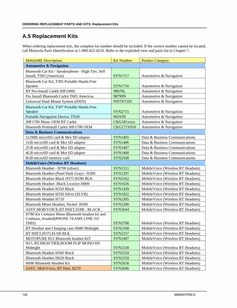
ORDERING REPLACEMENT PARTS AND KITS: Replacement Kits
A.5 Replacement Kits
When ordering replacement kits, the complete kit number should be included. If the correct number cannot be located, call Motorola Parts Identification at 1-800-422-4210. Refer to the exploded view and parts list in Chapter 7.
MobileME Description Kit Number Product Category Automotive & Navigation Bluetooth Car Kit / Speakerphone - High Tier, Self Install, T505 (Americas) SYN1717 Automotive & Navigation Bluetooth Car Kit, T305 Portable Hands-Free Speaker SYN1716 Automotive & Navigation BT Pro-Install CarkIt IHF1000r 98676L Automotive & Navigation Pro Install Bluetooth Carkit T605 Americas 98799N Automotive & Navigation Universal Dash Mount System (iDEN) NNTN7295 Automotive & Navigation Bluetooth Car Kit, T307 Portable Hands-Free Speaker SYN2715 Automotive & Navigation Portable Navigation Device, TN30 89293N Automotive & Navigation IHF1700 Music OEM BT Carkit CKG181xxxx Automotive & Navigation Bluetooth ProInstall Carkit IHF1700 OEM CKG171V010 Automotive & Navigation Data & Business Communications 512MB microSD card & Mot SD adapter SYN1405 Data & Business Communications 1GB microSD card & Mot SD adapter SYN1406 Data & Business Communications 2GB microSD card & Mot SD adapter SYN1407 Data & Business Communications 4GB microSD card & Mot SD adapter SYN1408 Data & Business Communications 8GB microSD memory card SYN2508 Data & Business Communications MobileVoice (Wireless BT Headsets) Bluetooth Headset - H700 (silver) SYN1311 MobileVoice (Wireless BT Headsets) Bluetooth Headset (Pearl Dark Gray) - H300 SYN1297 MobileVoice (Wireless BT Headsets) Bluetooth Headset Black H375 ROM BLK SYN2162 MobileVoice (Wireless BT Headsets) Bluetooth Headset -Black Licorice-H800 SYN1626 MobileVoice (Wireless BT Headsets) Bluetooth Headset H350 Black SYN1439 MobileVoice (Wireless BT Headsets) Bluetooth Headset H550 Silver (SLVR) SYN1822 MobileVoice (Wireless BT Headsets) Bluetooth Headset H710 SYN2305 MobileVoice (Wireless BT Headsets) Bluetooth Mono Headset, Nickel- H500 SYN1290 MobileVoice (Wireless BT Headsets) ASSY,MOB/VOICE,BT HSET,H390 , BLACK SYN2644 MobileVoice (Wireless BT Headsets) H780 Kit Contains Mono Bluetooth headset kit and Cushions, brushed(PHONE TEAMS LINK TO THIS) SYN2708 MobileVoice (Wireless BT Headsets) BT Headset and Charging case H680 Midnight SYN2168 MobileVoice (Wireless BT Headsets) BT HSET,H375,FLSH BLK SYN2257 MobileVoice (Wireless BT Headsets) MOTOPURE H12 Bluetooth headset KIT SYN2487 MobileVoice (Wireless BT Headsets) H15, BT,HIGH TIER,BOOM FLIP MONO HS Midnight SYN2530 MobileVoice (Wireless BT Headsets) Bluetooth Headset H560 Black SYN2518 MobileVoice (Wireless BT Headsets) Bluetooth Headset H620 Black SYN2259 MobileVoice (Wireless BT Headsets) H690 Bluetooth Headset Kit SYN2616 MobileVoice (Wireless BT Headsets) ASSY, Mob/Voice, BT Hset, H270 SYN2646 MobileVoice (Wireless BT Headsets)
142 6880401P59-O
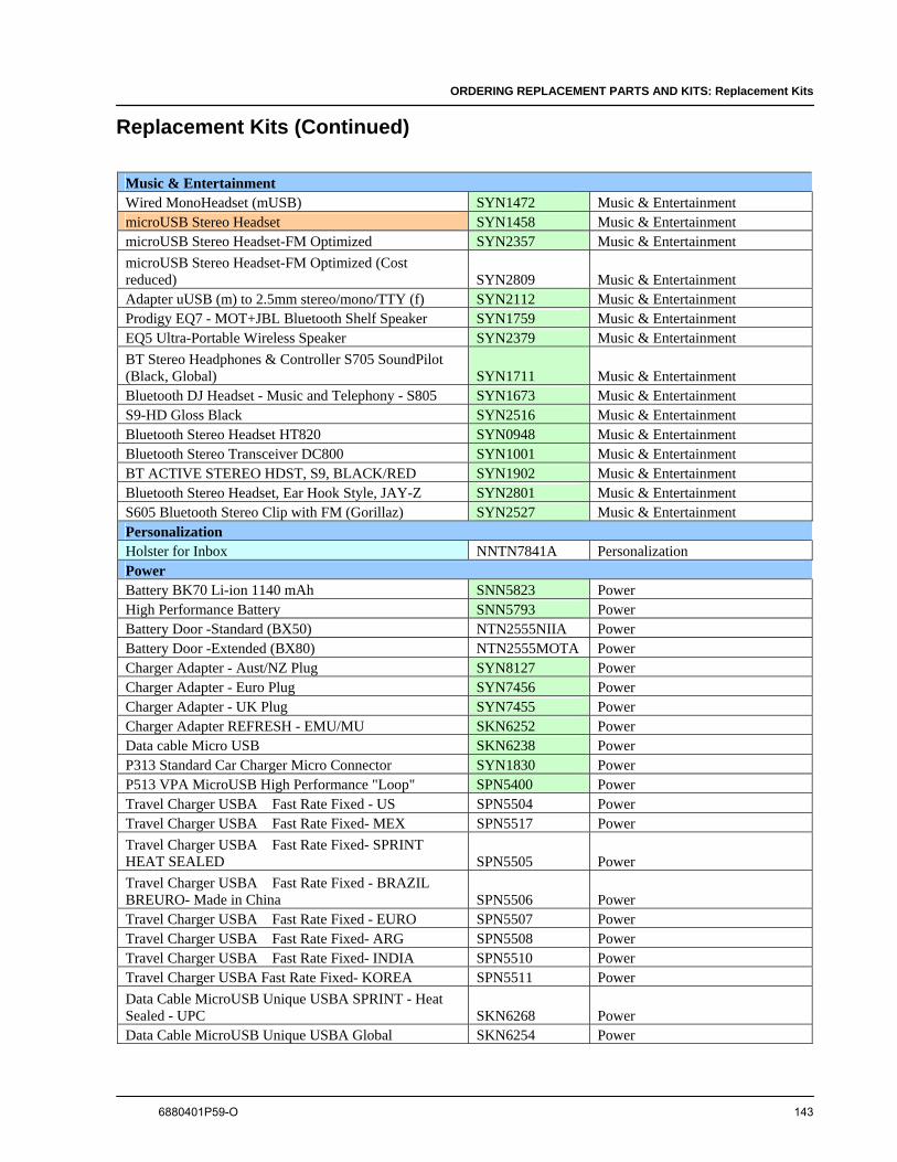
ORDERING REPLACEMENT PARTS AND KITS: Replacement Kits Replacement Kits (Continued)
Music & Entertainment Wired MonoHeadset (mUSB) SYN1472 Music & Entertainment microUSB Stereo Headset SYN1458 Music & Entertainment microUSB Stereo Headset-FM Optimized SYN2357 Music & Entertainment microUSB Stereo Headset-FM Optimized (Cost reduced) SYN2809 Music & Entertainment Adapter uUSB (m) to 2.5mm stereo/mono/TTY (f) SYN2112 Music & Entertainment Prodigy EQ7 - MOT+JBL Bluetooth Shelf Speaker SYN1759 Music & Entertainment EQ5 Ultra-Portable Wireless Speaker SYN2379 Music & Entertainment BT Stereo Headphones & Controller S705 SoundPilot (Black, Global) SYN1711 Music & Entertainment Bluetooth DJ Headset - Music and Telephony - S805 SYN1673 Music & Entertainment S9-HD Gloss Black SYN2516 Music & Entertainment Bluetooth Stereo Headset HT820 SYN0948 Music & Entertainment Bluetooth Stereo Transceiver DC800 SYN1001 Music & Entertainment BT ACTIVE STEREO HDST, S9, BLACK/RED SYN1902 Music & Entertainment Bluetooth Stereo Headset, Ear Hook Style, JAY-Z SYN2801 Music & Entertainment S605 Bluetooth Stereo Clip with FM (Gorillaz) SYN2527 Music & Entertainment Personalization Holster for Inbox NNTN7841A Personalization Power Battery BK70 Li-ion 1140 mAh SNN5823 Power High Performance Battery SNN5793 Power Battery Door -Standard (BX50) NTN2555NIIA Power Battery Door -Extended (BX80) NTN2555MOTA Power Charger Adapter - Aust/NZ Plug SYN8127 Power Charger Adapter - Euro Plug SYN7456 Power Charger Adapter - UK Plug SYN7455 Power Charger Adapter REFRESH - EMU/MU SKN6252 Power Data cable Micro USB SKN6238 Power P313 Standard Car Charger Micro Connector SYN1830 Power P513 VPA MicroUSB High Performance "Loop" SPN5400 Power Travel Charger USBA Fast Rate Fixed - US SPN5504 Power Travel Charger USBA Fast Rate Fixed- MEX SPN5517 Power Travel Charger USBA Fast Rate Fixed- SPRINT HEAT SEALED SPN5505 Power Travel Charger USBA Fast Rate Fixed - BRAZIL BREURO- Made in China SPN5506 Power Travel Charger USBA Fast Rate Fixed - EURO SPN5507 Power Travel Charger USBA Fast Rate Fixed- ARG SPN5508 Power Travel Charger USBA Fast Rate Fixed- INDIA SPN5510 Power Travel Charger USBA Fast Rate Fixed- KOREA SPN5511 Power Data Cable MicroUSB Unique USBA SPRINT - Heat Sealed - UPC SKN6268 Power Data Cable MicroUSB Unique USBA Global SKN6254 Power
6880401P59-O 143
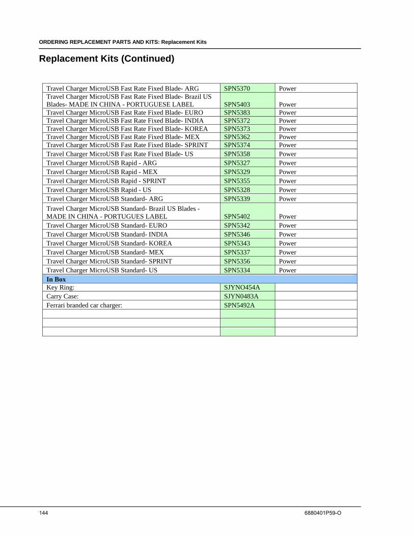
ORDERING REPLACEMENT PARTS AND KITS: Replacement Kits Replacement Kits (Continued)
Travel Charger MicroUSB Fast Rate Fixed Blade- ARG SPN5370 Power Travel Charger MicroUSB Fast Rate Fixed Blade- Brazil US Blades- MADE IN CHINA - PORTUGUESE LABEL SPN5403 Power Travel Charger MicroUSB Fast Rate Fixed Blade- EURO SPN5383 Power Travel Charger MicroUSB Fast Rate Fixed Blade- INDIA SPN5372 Power Travel Charger MicroUSB Fast Rate Fixed Blade- KOREA SPN5373 Power Travel Charger MicroUSB Fast Rate Fixed Blade- MEX SPN5362 Power Travel Charger MicroUSB Fast Rate Fixed Blade- SPRINT SPN5374 Power Travel Charger MicroUSB Fast Rate Fixed Blade- US SPN5358 Power Travel Charger MicroUSB Rapid - ARG SPN5327 Power Travel Charger MicroUSB Rapid - MEX SPN5329 Power Travel Charger MicroUSB Rapid - SPRINT SPN5355 Power Travel Charger MicroUSB Rapid - US SPN5328 Power Travel Charger MicroUSB Standard- ARG SPN5339 Power Travel Charger MicroUSB Standard- Brazil US Blades - MADE IN CHINA - PORTUGUES LABEL SPN5402 Power Travel Charger MicroUSB Standard- EURO SPN5342 Power Travel Charger MicroUSB Standard- INDIA SPN5346 Power Travel Charger MicroUSB Standard- KOREA SPN5343 Power Travel Charger MicroUSB Standard- MEX SPN5337 Power Travel Charger MicroUSB Standard- SPRINT SPN5356 Power Travel Charger MicroUSB Standard- US SPN5334 Power In Box Key Ring:
SJYNO454A Carry Case: SJYN0483A Ferrari branded car charger: SPN5492A
144 6880401P59-O
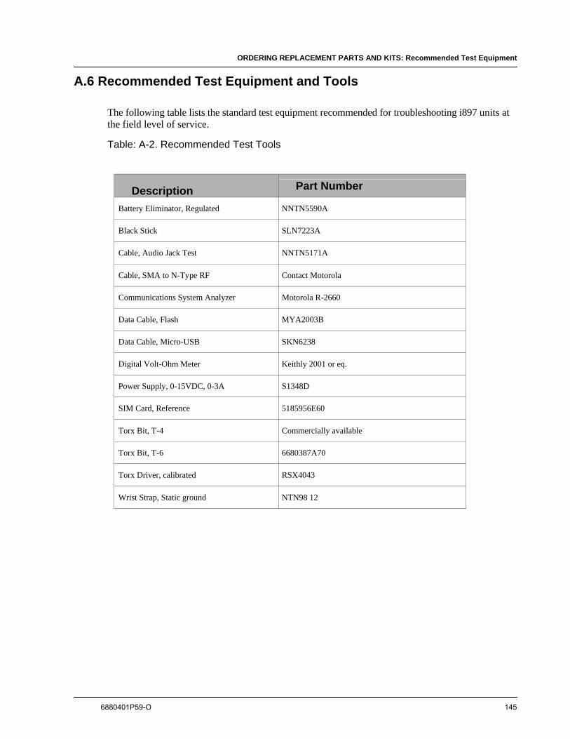
ORDERING REPLACEMENT PARTS AND KITS: Recommended Test Equipment
A.6 Recommended Test Equipment and Tools
The following table lists the standard test equipment recommended for troubleshooting i897 units at the field level of service.
Table: A-2. Recommended Test Tools
Description Part Number
Battery Eliminator, Regulated NNTN5590A
Black Stick SLN7223A
Cable, Audio Jack Test NNTN5171A
Cable, SMA to N-Type RF Contact Motorola
Communications System Analyzer Motorola R-2660
Data Cable, Flash MYA2003B
Data Cable, Micro-USB SKN6238
Digital Volt-Ohm Meter Keithly 2001 or eq.
Power Supply, 0-15VDC, 0-3A S1348D
SIM Card, Reference 5185956E60
Torx Bit, T-4 Commercially available
Torx Bit, T-6 6680387A70
Torx Driver, calibrated RSX4043
Wrist Strap, Static ground NTN98 12
6880401P59-O 145
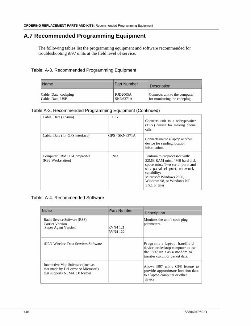
ORDERING REPLACEMENT PARTS AND KITS: Recommended Programming Equipment
A.7 Recommended Programming Equipment
The following tables list the programming equipment and software recommended for troubleshooting i897 units at the field level of service.
Table: A-3. Recommended Programming Equipment
Name Part Number Description
Cable, Data, codeplug Cable, Data, USB
RJD2005A SKN6371A
Connects unit to the computer for monitoring the codeplug.
Table A-3. Recommended Programming Equipment (Continued) Cable, Data (2.5mm) TTY
Connects unit to a teletypewriter (TTY) device for making phone calls.
Cable, Data (for GPS interface) GPS - SKN6371A Connects unit to a laptop or other device for sending location information.
Computer, IBM PC-Compatible N/A Pentium microprocessor with: (RSS Workstation) 32MB RAM min.; 4MB hard disk
space min.; Two serial ports and one para l le l por t ; ne twork- capability;
Microsoft Windows 2000, Windows 98, or Windows NT
3.5.1 or later
Table: A-4. Recommended Software
Name Part Number Description
Monitors the unit’s code plug parameters.
Radio Service Software (RSS) Carrier Version
RVN4 121 RVN4 122
Super Agent Version
Programs a laptop, handheld device, or desktop computer to use the i897 unit as a modem to transfer circuit or packet data.
iDEN Wireless Data Services Software
Interactive Map Software (such as that made by DeLorme or Microsoft) that supports NEMA 3.0 format
Allows i897 unit’s GPS feature to provide approximate location data to a laptop computer or other device.
146 6880401P59-O

6880401P59-O 147

© 2010 by Motorola, Inc. 8000 W. Sunrise Blvd. Ft. Lauderdale, FL 33322 All Rights Reserved.