manipulation of spin currents in metallic...
TRANSCRIPT

Phil. Trans. R. Soc. A (2011) 369, 3136–3149doi:10.1098/rsta.2011.0010
REVIEW
Manipulation of spin currents in metallicsystems
BY YOSHICHIKA OTANI1,* AND TAKASHI KIMURA2
1Institute for Solid State Physics, University of Tokyo, 5-1-5 Kashiwanoha,Kashiwa, Chiba 277-8581, Japan
2Inamori Frontier Research Center, Kyushu University, 744 Motooka,Fukuoka 819-0395, Japan
The transport properties of diffusive spin currents have been investigated in lateralferromagnetic/non-magnetic metal hybrid structures. The spin diffusion processes werefound to be strongly dependent on the magnitude of the spin resistances of connectedmaterials. Efficient spin injection and detection are accomplished by optimizing thejunction structures on the basis of the spin resistance circuitry. The magnetizationswitching of a nanoscale ferromagnetic particle and also room temperature spin Halleffect measurements were realized by using an efficient pure-spin-current injection.
Keywords: spin current; spin injection; spin torque; spin Hall effect; spin–orbit interaction
1. Introduction
There has been a great deal of interest in studying spin-electronic properties inferromagnetic (F)/non-magnetic (N) hybrid structures since the discovery of thegiant magnetoresistance (GMR) effect [1,2], where a spin current, i.e. a flow ofspin angular momentum, is a key ingredient [3,4]. Therefore, understanding thephysics responsible for spin currents and establishing efficient ways for mani-pulation are indispensable for further advancement of spin-electronic devices.
In N metals, the spin current flows with the non-equilibrium spin polarization,the magnitude of which decays via spin relaxation. The length scale over whichspin current flows is known as the spin-diffusion length, typically a few hundredsof nanometres. Most experiments on spin transport have been carried out so farwith vertical structures configured to have current perpendicular to the plane [5].In this way, the travelling length for the spin current in a non-magnet can beshortened below the spin-diffusion length. However, the vertical structures onlygive limited information about series resistances of magnetic multi-layers. Onthe contrary, laterally configured F/N hybrid devices have great advantages ofdeveloping multi-terminal devices. Recent nanofabrication techniques enable usto prepare structures where the travelling length of the spin current is comparable*Author for correspondence ([email protected]).
One contribution of 12 to a Theme Issue ‘New directions in spintronics’.
This journal is © 2011 The Royal Society3136
on June 4, 2018http://rsta.royalsocietypublishing.org/Downloaded from

Review. Manipulation of spin currents 3137
Py1
H
Py2
Cu
Ie
Ie
positive V
Vnegative
V–
V+100 nmI+
I–
(a)
(b)
(c)
Figure 1. (a) Scanning electron microscope image of a typical lateral spin-valve consisting of twoPy wires and a Cu wire. (b,c) Schematic illustrations of non-local detection of spin accumulation.The positive and negative voltages are induced between the F and N voltage probes for (b) paralleland (c) anti-parallel configurations, respectively. (Online version in colour.)
to or shorter than the spin-diffusion length, even in the lateral configuration. Inthis article, we investigate the diffusive spin transport in metallic F/N hybridlateral structures.
2. Electrical detection of spin accumulation induced by non-local spin injection
Despite the device dimension being smaller than the spin-diffusion length, it hasbeen difficult to detect spin-dependent signals in lateral structures owing to thespurious magnetoresistance effects, such as anisotropic magnetoresistance andanomalous Hall effects. Non-local spin injection, by which the spin and chargecurrents are well separated, is thus a useful means for detecting the spin current-induced signals in lateral configurations because irrelevant magnetoresistancechanges can be removed [6,7]. In this section, we explain the principle of theelectrical detection of the spin accumulation induced by a non-local spin injection.
Figure 1a shows a scanning electron microscope (SEM) image of a typicallateral spin-valve consisting of two permalloy (Py) wires bridged by a Cu wire.Lateral spin-valve is prepared by means of the undercut resist mask and shadowevaporation technique. First, the Py layer of 20 nm in thickness is formed byoblique evaporation at a pressure of 10−9 torr. After the Py deposition, the Cu of100 nm in thickness is evaporated from the normal to the substrate in a differentchamber with a base pressure of 2×10⁻⁷ torr. In order to reduce the magnetic imp-urity in the Cu film, the chamber for the Cu evaporation is separated from that forthe Py evaporation. Note here that these two chambers are connected in vacuum.
As shown in figure 1a, the electric current is injected from Py1 into the left-hand side of the Cu wire. Thereby, non-equilibrium spin accumulation is inducedin the vicinity of the junction. The accumulated spins diffuse not only into theleft-hand side of the Cu but also into the right-hand side of the Cu as shown infigure 1b. In this way, a spin current is produced with carrying no charge current(pure spin current) in the right-hand side. When another ferromagnet Py2 isconnected to the right-hand side of the Cu, spin splitting in the electrochemical
Phil. Trans. R. Soc. A (2011)
on June 4, 2018http://rsta.royalsocietypublishing.org/Downloaded from

3138 Y. Otani and T. Kimura
4(a) (b)
2
V/ I
(m
Ω)
0
–600 –300 0
Δ RS
Δ R
s (Ω
)
300magnetic field (Oe)
600500 1000 1500
T = 10 K
T = 290 K
distance (nm)2000
10–2
10–3
10–4
10–5
Figure 2. (a) Typical non-local spin-valve signal measured at 10 K. (b) Spin signal as a functionof the electrode distance between two Py wires at 290 K and 10 K. The solid and dotted lines arecalculated evolutions of the spin signal using equation (2.1) at 10 K and 290 K, respectively.
potential is induced in Py2 sufficient for the continuity condition of the chemicalpotential at the interface. The stationary point for the chemical potential inPy2 shifts from the central point because of the spin-dependent conductivity.Therefore, the voltage appears between Py2 and the right-hand side of the Cu wireas shown in figure 1b and the induced voltage changes its sign according to therelative magnetic configuration between Py1 and Py2. When Py1 is parallel (anti-parallel) to Py2, the induced voltage is positive (negative). Figure 2a shows thefield dependence of the non-local spin-valve (NLSV) signal, where the magneticfield is applied along the Py wires. Here, in the vertical axis, the non-local signal inohms is given by the induced voltage divided by the injecting current. The non-local signal exhibits the clear spin-valve effect corresponding to either parallel(high) or anti-parallel (low) state. We define here the spin signal as the resistancechange between the parallel and anti-parallel states.
We here evaluate the spin-diffusion length of the Cu wire from the spin signalmeasured as a function of separation d. The spin signals for various separationsfrom 250 to 1650 nm measured at 290 and 10 K are shown in figure 2b. The spinsignal decreases monotonically with the separation. From the one-dimensionalspin-diffusion model with the transparent Py/Cu interface, the dependence ofthe spin signal DRS on the separation d is deduced as [8,9]
DRS ≈ P2PyR
2SPy
2RSPy exp (d/lCu) + RSCu sinh (d/lCu). (2.1)
Here, PPy is the spin polarization for Py and lCu is the spin-diffusion length ofCu. RSPy and RSCu are the spin resistances for Py and Cu, respectively. The spinresistance is defined as 2rl/((1 − P2)S), with polarization P, resistivity r, spin-diffusion length l and the effective cross-sectional area for the spin current S . Weshow in the following sections that the spin resistance is an important measureto design the spin-dependent transport property of the system.
From the curve fitting, we obtain the spin-diffusion length for the Cu wire as400 nm at 290 K and 1000 nm at 10 K. The spin polarization and the spin-diffusionlength for Py are 0.49 and 4.5 nm at room temperature and then 0.58 and 5 nmat 10 K. The spin-diffusion length of the Py is in good agreement with previouslyreported values [7,9].
Phil. Trans. R. Soc. A (2011)
on June 4, 2018http://rsta.royalsocietypublishing.org/Downloaded from
Review. Manipulation of spin currents 3139
1.0(a) (b) 1.5
1.0
0.5
λ Cu
(μm
)
ρ Cu
(μΩ
cm)
2
1
0
0.8
0.6
0.4
Δ R
S (m
Ω)
0.2
0 100 200T (K) T (K)
300 0 100 200 300
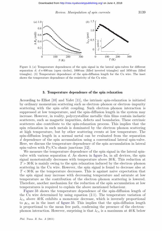
Figure 3. (a) Temperature dependences of the spin signal in the lateral spin-valves for differentseparation d; d = 600 nm (open circles), 1000 nm (filled inverted triangles) and 1650 nm (filledtriangles). (b) Temperature dependence of the spin-diffusion length for the Cu wire. The insetshows the temperature dependence of the resistivity of the Cu wire.
3. Temperature dependence of the spin relaxation
According to Elliot [10] and Yafet [11], the intrinsic spin-relaxation is initiatedby ordinary momentum scattering such as electron–phonon or electron–impurityscattering with the spin–orbit coupling. Such electron–phonon interaction issuppressed at low temperature, and the spin-diffusion length in the system mayincrease. However, in reality, polycrystalline metallic thin films contain inelasticscatterers, such as magnetic impurities, defects and boundaries. These extrinsicscatterers also contribute to the spin-relaxation process. This implies that thespin relaxation in such metals is dominated by the electron–phonon scatteringat high temperature, but by other scattering events at low temperature. Thespin-diffusion length in a normal metal can be evaluated from the separationd dependence of the spin accumulation using a conventional lateral spin-valve.Here, we discuss the temperature dependence of the spin accumulation in lateralspin-valves with Py/Cu ohmic junctions [12].
We measure the temperature dependence of the spin signal in the lateral spin-valve with various separation d. As shown in figure 3a, in all devices, the spinsignal monotonically decreases with temperature above 30 K. This reduction atT > 30 K is mainly owing to the spin relaxation induced by the electron–phononscattering in the Cu wire. However, the spin signal is found to decrease also atT < 30 K as the temperature decreases. This is against naive expectation thatthe spin signal may increase with decreasing temperature and saturate at lowtemperature as the contribution of the electron–phonon scattering is lowered.Therefore, another mechanism for the reduction of the spin accumulation at lowtemperatures is required to explain the above mentioned behaviour.
Figure 3b shows the temperature dependence of the spin-diffusion length ofthe Cu wire determined by using equation (2.1). The temperature variation oflCu above 40 K exhibits a monotonic decrease, which is inversely proportionalto rCu as in the inset of figure 3b. This implies that the spin-diffusion lengthis proportional to the mean free path, confirming the presence of the electron–phonon interaction. However, surprising is that lCu is a maximum at 40 K below
Phil. Trans. R. Soc. A (2011)
on June 4, 2018http://rsta.royalsocietypublishing.org/Downloaded from
3140 Y. Otani and T. Kimura
which lCu decreases rapidly with temperature. It should be noted that the spin-diffusion length and spin polarization of Py determined from the experimentsonly slightly decrease in this temperature range.
Thus, the reduction of the spin signal below 40 K is likely owing to the reductionof lCu. The spin-diffusion length l is given by
√Dtsf , where D and tsf are the
diffusion constant and the spin-relaxation time, respectively. As seen in the insetof figure 3b, the resistivity of the Cu wire slightly decreases even below 40 Kwith temperature, implying that the mean free path l for the electrons in theCu wire increases with decreasing temperature. Since D is proportional to themean free path, the reduction in lCu should be owing to the reduction of tsf .A possible reason for the reduction is the surface oxidation. As Cu surfacesare known to be reactive in air, the top and side surfaces of the Cu wire maybe oxidized. The oxidized regions provide stronger spin-flip scatterers than theinside of the Cu wire [13]. Therefore, the spin-flip scattering owing to the oxidizedCu is more pronounced as the mean free path is increased at low temperatures.This explains the reduction of the spin-diffusion length at low temperatures below40 K. The ratio of the elastic scattering time to the spin-flip scattering time, te/tsf ,represents the strength of the spin–orbit interaction. The relation te = l/vf withthe Fermi velocity vf yields the ratio te/tsf = 2.74 × 10⁻³ at 290 K and 4.64 × 10⁻³
at 10 K, agreeing with the scenario that the spin-flip scattering is mediatedby the exchange interaction with small magnetic moment in the copper oxide.This means that the spin–orbit interaction becomes large at low temperatures,supporting that the reduction of tsf is due to the scattering of the oxidized layer.
4. Influence of an additional ohmic contact
In the NLSV measurement, an F wire is commonly used to detect the spin accu-mulation in the N wire. However, we have to take into account that the ferro-magnet with a low interface resistance significantly affects the distribution of thespin-dependent electrochemical potential in the N wire because the spin currentis preferably absorbed and equilibrated in the F wire. In this section, we showthe non-trivial influence of an additional ohmic contact on the spin accumulationand also spin current using a lateral spin-valve device with a middle wire [14].
Figure 4 shows the suppression of the spin accumulation can be demonstratedin the NLSV measurement using a lateral spin-valve consisting of three Py wiresand a Cu wire. As mentioned above, the Py middle wire connected to the Cuwire reduces the spin splitting of the chemical potential and also the spin signalmeasured with the Py1 and Py3 leads. The obtained small spin signal of 0.04 mUcoincides well with the above expectation. The geometrical defect owing to theadditional F contact lying beneath the Cu wire may also violate the distributionof the spin accumulation. However, we believe that such an effect is negligiblebecause of large difference in thickness between Cu and Py.
For comparison, we also fabricated a lateral spin-valve consisting of two Pywires separated by 600 nm spacing, longer than the spacing of 460 nm betweenPy1 and Py3 in figure 4a. The thickness and the width of Py and Cu wires arethe same as those of the previous spin-valve device consisting of three Py wires.The SEM image of the fabricated device is shown in the inset of figure 4b. If thereis no suppression owing to an additional Py wire in the previous experiment, the
Phil. Trans. R. Soc. A (2011)
on June 4, 2018http://rsta.royalsocietypublishing.org/Downloaded from

Review. Manipulation of spin currents 3141
0
(a) (b)
ΔV/I
(m
Ω)
–1.0–500 –400–200 200 400 6000–250 2500
magnetic field (Oe) magnetic field (Oe)
–0.5 Py1Py2Py3
I I
V V
Figure 4. (a) Non-local spin-valve signal for a lateral spin-valve consisting of three Py wires withthe middle Py wire. The inset shows an SEM image of the device and the probe configuration forthe measurement. (b) Non-local spin-valve signal for a lateral spin-valve consisting of two Py wireswith a spacing of 600 nm. The inset shows an SEM image of the device and the probe configurationfor the measurement.
spin signal of figure 4b should be smaller by a factor of about 0.7 than that offigure 4b. Figure 4b shows the spin signal measured in the probe configurationshown in the inset. The obtained spin signal is 0.2 mU, much larger than thatof figure 4a. These results support that the spin accumulation in the N wireis reduced by the F wire connected to the N wire. Note here that no change isobserved in the spin signal with the middle Py wire indicating that the magnitudeof the spin current absorption does not depend on the magnetization configurationof the middle wire.
We also demonstrate that the spin accumulation is reduced by connecting theN wire with a small spin resistance. For this purpose, lateral spin-valves consistingof triple junctions were prepared with various middle (M) wires as in figure 5a.Figure 5b shows the spin signal of the device with the Au M wire. The obtainedspin signal is 0.08 mU, showing the large reduction in the spin signal similar tothat of the Py M wire. This implies that the Au wire has smaller spin resistance.
The spin signal DRS can be approximated to be a function of spin resistanceRSM of the middle wire [9]:
DRS ≈ P2Py
(RSPy/RSCu
)2 RSM
4 ((cosh (d/lN) − 1) + (RSM/RSCu) sinh (d/lN)). (4.1)
By putting into equation (4.1) the values of spin resistances RSPy and RSCudetermined in the previous double junction experiments, we obtain the followingrelation between the detected spin signal RNLSV and RSM:
RSM(U) = 7.02RNLSV(mU)1.27 − 4.41RNLSV(mU)
. (4.2)
This equation provides a useful means to estimate the spin resistance andthe spin-diffusion length of the middle wire from the magnitude of the spinsignal without varying the spacing d. Below is described a test experiment forvarious materials: Cu, Au and Py. In this calculation, the spin signal with themiddle wire insertion does not depend on the magnetization configuration of themiddle wire.
Phil. Trans. R. Soc. A (2011)
on June 4, 2018http://rsta.royalsocietypublishing.org/Downloaded from

3142 Y. Otani and T. Kimura
1
10–1
10–2
Cu wire
Au wire Py wires
–0.2
0.2
(a)
(b)
(c)Cu
Au
Py
–0.4–500 –250 250 500
0 0.1 0.2
magnetic field (Oe)
0
0
ΔV/I
(m
Ω)
RSM
(Ω
)
RNLSV (mΩ)
Figure 5. (a) SEM image of a typical lateral spin device consisting of double Py/Cu junctions anda middle Au/Cu junction. (b) Non-local spin-valve curve with Au middle insertions. (c) Calculatedspin resistance as a function of the obtained non-local spin signal RNLSV.
Figure 5c shows the spin resistance of the M wire RSM as a function of RNLSVdeduced from equation (4.2). From the equation, we respectively obtain the spinresistances of the Cu, Au and Py wires as 2.67, 0.62 and 0.33 U. The experimentalvalues for the Py and Cu M wires are quantitatively in good agreement with thoseobtained from the double junction confirming the validity of equation (4.2). Forthe Au wire, the resistivity of 5.24 mU cm of the Au strip yields a spin-diffusionlength of 60 nm. This is in good agreement with the other reported values [15]and proves that the Au wire has short spin-diffusion length owing to the strongspin–orbit interaction [16].
5. Efficient spin accumulation by reducing junction size
As discussed above, the spatial distribution of the spin current and accumulationcan be calculated by introducing the spin resistance [9]. The calculation showsthat the spin accumulation and current depend not only on the electrode spacingbut also on the spin resistance of each constituent segment, whose magnitudevaries with the effective cross-sectional area S . Therefore, the spin polarizationinduced in N should depend on the effective cross-sectional area, equivalent toF/N junction size. In this section, we experimentally demonstrate that the size ofthe ohmic F/N junction is an important structural factor for obtaining large spinaccumulation in N and that both the spin polarization and the spin resistanceof F are enhanced by optimizing the junction size [17,18].
The difference in the junction size between injector and detector gives riseto a significant difference in the spin resistance. In a cross-shaped Cu wire, theeffective spin resistances of the vertical Cu arms are much smaller than thoseof the horizontal Cu arms because the vertical Cu arms have additional ohmiccontacts with the Py pad and wire. This allows us to neglect the spin current
Phil. Trans. R. Soc. A (2011)
on June 4, 2018http://rsta.royalsocietypublishing.org/Downloaded from
Review. Manipulation of spin currents 3143
19.8
I+
I+
V+
V+
I–
I–
V–
V–
V/I
(m
Ω)
V/I
(m
Ω)
19.7
6.0
5.5
5.0
1.0
0.8
0.6
0.4
spin
sig
nal (
mΩ
)
0.2
0 0.1
600 nm
w
lp
junction size, lpw (μm2)
junction size, lpw
0.2
–600 –300 0magnetic field (Oe)
300 600
(a)
(b)
(c)
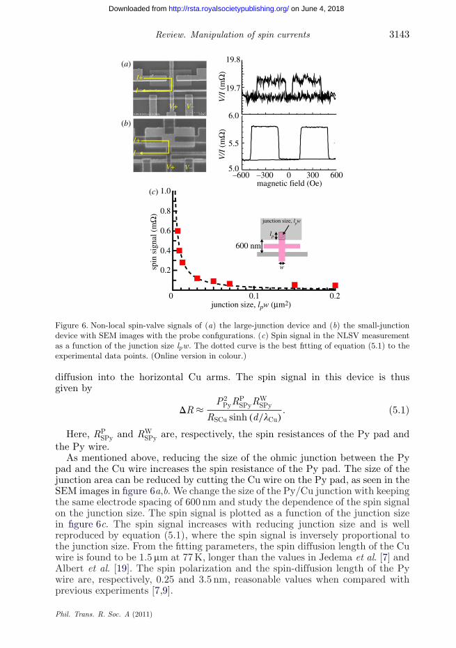
Figure 6. Non-local spin-valve signals of (a) the large-junction device and (b) the small-junctiondevice with SEM images with the probe configurations. (c) Spin signal in the NLSV measurementas a function of the junction size lpw. The dotted curve is the best fitting of equation (5.1) to theexperimental data points. (Online version in colour.)
diffusion into the horizontal Cu arms. The spin signal in this device is thusgiven by
DR ≈ P2PyR
PSPyR
WSPy
RSCu sinh (d/lCu). (5.1)
Here, RPSPy and RW
SPy are, respectively, the spin resistances of the Py pad andthe Py wire.
As mentioned above, reducing the size of the ohmic junction between the Pypad and the Cu wire increases the spin resistance of the Py pad. The size of thejunction area can be reduced by cutting the Cu wire on the Py pad, as seen in theSEM images in figure 6a,b. We change the size of the Py/Cu junction with keepingthe same electrode spacing of 600 nm and study the dependence of the spin signalon the junction size. The spin signal is plotted as a function of the junction sizein figure 6c. The spin signal increases with reducing junction size and is wellreproduced by equation (5.1), where the spin signal is inversely proportional tothe junction size. From the fitting parameters, the spin diffusion length of the Cuwire is found to be 1.5 mm at 77 K, longer than the values in Jedema et al. [7] andAlbert et al. [19]. The spin polarization and the spin-diffusion length of the Pywire are, respectively, 0.25 and 3.5 nm, reasonable values when compared withprevious experiments [7,9].
Phil. Trans. R. Soc. A (2011)
on June 4, 2018http://rsta.royalsocietypublishing.org/Downloaded from

3144 Y. Otani and T. Kimura
0.2
injector injector
Ie
μ1
μynormal
particle
(a) (b)
(c) (d)
particle
V–
IS
Ic
0.1
V/I
(m
Ω)
0
–2000 2000 –20 –10 0Iamp (mA)
10
parallel
anti-parallel
20–1000 10000
0.18 mΩ0.18 mΩ
magnetic field (Oe)
400 nm
Py particle
Py injector
Figure 7. (a) Schematic illustration of non-local spin injection using lateral spin-valve geometry.Only spin current is injected into the small F particle. (b) SEM image of the fabricated lateralspin-valve. The device consists of a large 30 nm thick Py injector, a Cu cross 100 nm wide and80 nm thick and a Py nanoscale particle, 50 nm wide, 180 nm long and 6 nm thick. (c) Fielddependence of the non-local spin signal. The changes in resistance at low and high fieldscorrespond to the relative magnetic switching of the Py injector and particle, from parallel to anti-parallel states and vice versa. (d) Non-local spin-valve signal after pulsed current injection as afunction of the current amplitude with corresponding magnetization configurations. (Online versionin colour.)
6. Magnetization switching owing to spin current absorption
Current-induced magnetization reversal is one of the key technologies fordeveloping spintronic devices. The switching mechanism owing to spin torqueis explained with a model proposed by Slonczewski in which the torque exertedon the magnetization is proportional to the injected spin current. This clearlyindicates that the spin current is essential to realize the magnetization switchingowing to the spin injection. Most of the present spin-transfer devices consistof vertical multi-layered nanopillars in which typically two magnetic layers areseparated by an N metal layer [19,20]. In such vertical structures, the chargecurrent always flows together with the spin current, and thereby undesirable Jouleheat is generated. As discussed in §4, the spin currents are effectively absorbedinto an additionally connected metallic wire with a small spin resistance. Thisimplies that the spin current without a charge flow can be selectively injected intoan F particle with a small spin resistance, such as a Py particle, once replacedwith the wire so that the pure spin current may contribute to the spin torque.To test this idea, a nanoscale F particle is configured for a lateral non-local spininjection device as in figure 7a,b [21].
Phil. Trans. R. Soc. A (2011)
on June 4, 2018http://rsta.royalsocietypublishing.org/Downloaded from
Review. Manipulation of spin currents 3145
The device consists of a large Py pad 30 nm in thickness, a Cu cross 100 nmin width and 80 nm in thickness, and a Py nanoscale particle, 50 nm in width,180 nm in length and 6 nm in thickness. A gold wire of 100 nm in width and 40 nmin thickness is connected to the Py particle to reduce the effective spin resistance,resulting in high-spin current absorption into the Py particle. The magnetic field isapplied along the easy axis of the Py particle. Note here that the dimensions of Pypad and Cu wires are chosen large enough to carry a charge current up to 15 mA.
To confirm whether the spin current from the Py injector is absorbed intothe Py particle, NLSV measurements are performed. As in figure 7c, the fielddependence shows a clear spin signal with a magnitude of 0.18 mU, ensuring thatthe spin current reaches the Py particle. Then, we examine the effect of thenon-local spin injection into the Py particle using the same probe configuration.Before performing the non-local spin injection, the magnetization configuration isset in the anti-parallel state by controlling the external magnetic field. The non-local spin injection is performed by applying large pulsed currents up to 15 mAin the absence of magnetic field. As shown in figure 7d, when the magnitudeof the pulsed current is increased positively in the anti-parallel state, no signalchange is observed up to 15 mA. While for the negative scan an abrupt signalchange is observed at −14 mA. The change in resistance at −14 mA is 0.18 mU,corresponding to that of the transition from anti-parallel to parallel states. Thismeans that the magnetization of the Py particle is switched only by the non-local spin current. The spin current responsible for switching is estimated fromthe experiment to be about 200 mA, which is reasonable compared with the valuesobtained for conventional pillar structures. However, the observed switching wasonly from the anti-parallel to parallel state in the device. This is mainly owingto the low spin injection efficiency.
To improve the efficiency of the injecting spin current, we have fabricated thenewly designed sample shown in figure 8a consisting of two Py/Au nanopillars ona Cu wire [22]. As shown in figure 8a, the junction size between the Py/Cu in thenew sample is effectively diminished, leading to the enhanced spin resistance forthe Py. Figure 8b shows the NLSV signal as a function of the external field. Theobtained spin signal is around 4 mU, much larger than previously reported values.Then, non-local spin injection with variable DC current between contacts 3 and 6is applied to switch the magnetization of the Py/Au nanopillar. The sample isset in a parallel state (denoted as A) at which both magnetizations are alignedin the positive field direction. As can be seen in figure 8c, when the current isincreased, the NLSV signal exhibits a sharp drop at about 5 mA, correspondingto a clear magnetization reversal from the parallel state A to the anti-parallelstate (denoted as B), which is switched back to the parallel state A by a negativeDC current of 5 mA. In this way, reversible magnetization switching between anti-parallel and parallel states is demonstrated by means of non-local spin injectionwith the specially developed device consisting of perpendicular nanopillars andlateral magnetic nanostructures.
7. Electrical detection of spin Hall effect
Electron trajectories are influenced by the interaction between the electron spinand the orbital angular momentum. This is known as the spin–orbit interaction,which induces non-trivial physical properties such as anomalous Hall effects in
Phil. Trans. R. Soc. A (2011)
on June 4, 2018http://rsta.royalsocietypublishing.org/Downloaded from

3146 Y. Otani and T. Kimura
3
5
V–+
1 3
2
detector
(a)
(b) (c)
injector
4
6
270 nm
Cu wire
Py/Au nanopillarsI
Is
2
1
0
V/I
(m
Ω)
–1
–2
3
2
1
0
–1
–2
–8 –6 –4 –2 0
A
–1
B
P
AP
IDC (mA)2 4 6 8–1.5 –1.0 –0.5 0.5
AP
P
H (kOe)1.0 1.50
Figure 8. (a) SEM image and schematic illustration of the improved non-local spin injection device.(b) Giant spin signal and (c) the reversible magnetization switching by pure spin current injectionobserved in the improved device. (Online version in colour.)
ferromagnets [23]. Even in non-magnets, the spin–orbit interaction is a dominantmechanism for spin-flip scattering causing spin decoherence. However, recently,the scattering owing to the spin–orbit interaction has been found to inducethe spin current in non-magnets via the spin Hall effect (SHE) [24,25]. Therehas been no experimental demonstration although the SHE was theoreticallypredicted a long time ago [26]. However, recent progress in spin injectionand detection techniques enables us to study the SHEs in N materials. Sincethe SHE can be used for generating the spin current without ferromagnets,exploring materials with large SHE is a challenging issue from the technologicalviewpoint.
A first clear observation of the SHE in a metallic system was reported byapplying non-local spin injection technique to a CoFe–Al hybrid structure [27].However, the observation is limited to low temperature because of the smallspin–orbit interaction in Al. To induce large SHE, the material should containspin–orbit scatterers. Platinum is known to exhibit large spin–orbit interactionbecause of its large atomic number. The conventional lateral structure for non-local spin injection cannot be employed to measure the SHE for Pt because ofthe extremely short spin-diffusion length of about a few nanometres [28]. Here,we show clear observation of direct and inverse SHEs induced in a Pt wire atroom temperature using the spin current absorption technique discussed in §4[21]. This technique allows us to detect the spin Hall signal generated over thenanoscale spin-diffusion length.
An SEM image of the device used for the present SHE experiment is shown infigure 9a. The device consists of a large Py pad 30 nm in thickness, a Cu cross100 nm in width and 80 nm in thickness and a Pt wire 80 nm in width and 4 nmin thickness. The distance from the centre of the injector to the centre of the Pt
Phil. Trans. R. Soc. A (2011)
on June 4, 2018http://rsta.royalsocietypublishing.org/Downloaded from

Review. Manipulation of spin currents 3147
Cu
Cu(a)
(b) (c)
Cu 1 2 31 2 3
Cu
Cu
1 2 3
Is
ISIe
Ie
IS
s
Pt
Py
Py
Py
PtCu
Pty
x
zy
x
Figure 9. (a) SEM image of the fabricated spin Hall device together with a schematic illustration ofthe fabricated device. (b) Schematic spin-dependent electrochemical potential map indicating spinaccumulation in Cu and Pt induced by the spin injection from the Py pad. Dashed line representsthe equilibrium position. (c) Schematic illustration of the charge accumulation process in the Ptwire, where IS and Ie denote injected pure spin current and induced charge current, respectively.(Online version in colour.)
wire is 400 nm. When the charge current is injected from an F Py pad into anN Cu cross and drained from one of the two arms (figure 9b), the non-local spincurrent is preferably absorbed into the Pt wire with strong spin–orbit interaction.
The spin currents injected into the Pt wire are converted to the transversecharge current voltage via the spin–orbit scattering. When the spin current ispolarized along the x-axis, the spin–orbit scattering induces the charge currentalong the Pt wire as schematically shown in figure 9c. Under the open circuitcondition, the charge current is balanced with the electric field owing to thecharge accumulation. Thus, the spin currents injected into the Pt wire producethe charge Hall voltage along the Pt wire. This phenomenon is known as theinverse SHE.
Figure 10 shows the field dependence of the voltage in the Pt wire induced bythe inverse SHE measured at room temperature and 77 K. Here, the magnitude ofthe effect is conventionally given in ohms by the voltage divided by the injectingcurrent in the Py/Cu junction. The angular dependence measurements of theinverse SHE reveal that the induced voltage is proportional to the in-plane xcomponent of the Py injector magnetization. This is an advantage in controllingthe injector magnetization because of low saturation field of the order of a fewhundred oersteds.
8. Conclusion
We have studied the spin-diffusion processes in lateral spin-valve structuresconsisting of Py/Cu ohmic junctions. The spin-diffusion length of the Cu wireis found to decrease at low temperature because of the enhancement of the
Phil. Trans. R. Soc. A (2011)
on June 4, 2018http://rsta.royalsocietypublishing.org/Downloaded from

3148 Y. Otani and T. Kimura
0.05(a)
(b)
sweepdirection
–0.05
0
0.10
0.05
HIe
M Vc
ΔRSHE0
–0.05
–0.10–2000 –1000 1000 20000
magnetic field (Oe)
ΔVc/
I (m
Ω)
ΔVc/
I (m
Ω)
Figure 10. The resistance change owing to the inverse SHE measured at (a) room temperatureand (b) 77 K. (Online version in colour.)
surface spin-flip scattering. We also found that the spin current and the spinaccumulation can be manipulated by additionally connected wires which act asspin absorber or spin-relaxation volume. The magnetization switching by purespin current injection and electrical detection of the SHE were demonstrated byusing efficient spin current absorptions.
References
1 Baibich, M. N., Broto, J. M., Fert, A., Nguyen Van Dau, F., Petroff, F., Eitenne, P., Creuzet,G., Friederich, A. & Chazelas, J. 1988 Giant magnetoresistance of (001)Fe/(001)Cr magneticsuperlattices. Phys. Rev. Lett. 61, 2472–2475. (doi:10.1103/PhysRevLett.61.2472)
2 Binasch, G., Grunberg, P., Saurenbach, F. & Zinn, W. 1989 Enhanced magnetoresistance inlayered magnetic structures with antiferromagnetic interlayer exchange. Phys. Rev. B 39, 4828–4830. (doi:10.1103/PhysRevB.39.4828)
3 Wolf, S. A., Awschalom, D. D., Buhrman, R. A., Daughton, J. M., von Molnar, S., Roukes,M. L., Chtchelkanova, A. Y. & Treger, D. M. 2001 Spintronics: a spin-based electronics visionfor the future. Science 294, 1488–1495. (doi:10.1126/science.1065389)
4 Zutic, I., Fabian, I. & Das Sarma, S. 2004 Spintronics: fundamentals and applications. Rev.Mod. Phys. 76, 323–410. (doi:10.1103/RevModPhys.76.323)
5 Pratt Jr, W. P., Lee, S.-F., Slaughter, J. M., Loloee, R., Schroeder, P. A. & Bass, J. 1991Perpendicular giant magnetoresistances of Ag/Co multilayers. Phys. Rev. Lett. 66, 3060–3063.(doi:10.1103/PhysRevLett.66.3060)
6 Johnson, M. & Silsbee, R. H. 1985 Interfacial charge–spin coupling: injection anddetection of spin magnetization in metals. Phys. Rev. Lett. 55, 1790–1793. (doi:10.1103/PhysRevLett.55.1790)
Phil. Trans. R. Soc. A (2011)
on June 4, 2018http://rsta.royalsocietypublishing.org/Downloaded from
Review. Manipulation of spin currents 3149
7 Jedema, F. J., Filip, A. T. & van Wees, B. J. 2001 Electrical spin injection and accumulationat room temperature in an all-metal mesoscopic spin valve. Nature 410, 345–348. (doi:10.1038/35066533)
8 Takahashi, S. & Maekawa, S. 2003 Spin injection and detection in magnetic nanostructures.Phys. Rev. B 67, 052409. (doi:10.1103/PhysRevB.67.052409)
9 Kimura, T., Hamrle, J. & Otani, Y. 2005 Estimation of spin-diffusion length from the magnitudeof spin-current absorption: multi-terminal ferromagnetic/non-ferromagnetic hybrid structures.Phys. Rev. B 72, 014461. (doi:10.1103/PhysRevB.72.014461)
10 Elliott, R. J. 1954 Theory of the effect of spin–orbit coupling on magnetic resonance in somesemiconductors. Phys. Rev. 96, 266–279. (doi:10.1103/PhysRev.96.266)
11 Yafet, Y. 1963 g Factors and spin-lattice relaxation of conduction electrons. In Solid statephysics, vol. 14 (eds F. Seitz & D. Turnbull), pp. 2–98. New York, NY: Academic press.
12 Kimura, T., Sato, T. & Otani, Y. 2008 Temperature evolution of spin relaxation in a NiFe/Culateral spin valve. Phys. Rev. Lett. 100, 066602. (doi:10.1103/PhysRevLett.100.066602)
13 Yuasa, S., Katayama, T., Nyvlt, M., Suzuki, Y. & Yori, T. 1998 Magnetoresistance in singleFe(001) ultrathin films. J. Appl. Phys. 83, 7031–7033. (doi:10.1063/1.367842)
14 Kimura, T., Hamrle, J., Otani, Y., Tsukagoshi, K. & Aoyagi, Y. 2004 Suppression of spinaccumulation in non-magnet due to ferromagnetic ohmic contact. Appl. Phys. Lett. 85, 3795–3796. (doi:10.1063/1.1811801)
15 Chiang, W. C., Ritz, C., Eid, K., Loloee, R., Pratt, W. P. & Bass, J. 2004 Search for mean-free-path effects in current-perpendicular-to-plane magnetoresistance. Phys. Rev. B 69, 184405.(doi:10.1103/PhysRevB.69.184405)
16 Pannetier, B., Chaussy, J., Rammal, R. & Gandit, P. 1985 First observation of Altshuler–Aronov–Spivak effect in gold and copper. Phys. Rev. B 31, 3209–3211. (doi:10.1103/PhysRevB.31.3209)
17 Kimura, T., Otani, Y. & Hamrle, J. 2006 Switching magnetization of a nanoscaleferromagnetic particle using non-local spin injection. Phys. Rev. Lett. 96, 037201. (doi:10.1103/PhysRevLett.96.037201)
18 Kimura, T., Otani, Y. & Hamrle, J. 2006 Enhancement of spin accumulation in a non-magneticlayer by reducing junction size. Phys. Rev. B 73, 132405. (doi:10.1103/PhysRevB.73.132405)
19 Albert, F. J., Emley, N. C., Myers, E. B., Ralph, D. C. & Buhrman, R. A. 2002 Quantitativestudy of magnetization reversal by spin-polarized current in magnetic multilayer nanopillars.Phys. Rev. Lett. 89, 266802. (doi:10.1103/PhysRevLett.89.226802)
20 Tsoi, M., Jansen, A. G. M., Bass, J., Chiang, W.-C., Seck, M., Tsoi, V. & Wyder, P. 1998Excitation of a magnetic multilayer by an electric current. Phys. Rev. Lett. 80, 4281–4284.(doi:10.1103/PhysRevLett.80.4281)
21 Kimura, T., Otani, Y., Sato, T., Takahashi, S. & Maekawa, S. 2007 Room-temperaturereversible spin Hall effect. Phys. Rev. Lett. 98, 156601. [Erratum in Phys. Rev. Lett. 2007,98, 249901(E). (doi:10.1103/PhysRevLett.98.249901)] (doi:10.1103/PhysRevLett.98.156601)
22 Yang, T., Kimura, T. & Otani, Y. 2008 Giant spin-accumulation signal and pure spin-current-induced reversible magnetization switching. Nat. Phys. 4, 851–854. (doi:10.1038/nphys1095)
23 Miyasato, T., Abe, N., Fujii, T., Asamitsu, A., Onoda, S., Onose, Y., Nagaosa, N. & Tokura, Y.2007 Crossover behavior of the anomalous Hall effect and anomalous Nernst effect in itinerantferromagnets. Phys. Rev. Lett. 99, 086602. (doi:10.1103/PhysRevLett.99.086602)
24 Hirsh, J. E. 1999 Spin Hall effect. Phys. Rev. Lett. 83, 1834–1837. (doi:10.1103/PhysRevLett.83.1834)
25 Zhang, S. 2000 Spin Hall effect in the presence of spin diffusion. Phys. Rev. Lett. 85, 393–396.(doi:10.1103/PhysRevLett.85.393)
26 Dyakonov, M. I. 1971 Current-induced spin orientation of electrons in semiconductors. JETPLett. 13, 467–469.
27 Valenzuela, S. O. & Tinkham, M. 2006 Direct electronic measurement of the spin Hall effect.Nature 442, 176–179. (doi:10.1038/nature04937)
28 Kurt, H., Loloee, R., Eid, K., Pratt Jr, W. P. & Bass, J. 2002 Spin-memory loss at 4.2 K insputtered Pd and Pt and at Pd/Cu and Pt/Cu interfaces. Appl. Phys. Lett. 81, 4787–4789.(doi:10.1063/1.1528737)
Phil. Trans. R. Soc. A (2011)
on June 4, 2018http://rsta.royalsocietypublishing.org/Downloaded from