manchester 09/sept/2008 a.falou & p.cornebise {lal-orsay} 1 slab integration & thermal...
TRANSCRIPT

Manchester 09/sept/2008
A.Falou & P.Cornebise {LAL-Orsay} 1
SLAB Integration & Thermal MeasurementsSlides Overview
Thermal Measurements (Demonstrator) Detector SLAB Integration Open Questions Conclusion/ Next Items

Manchester 09/sept/2008
A.Falou & P.Cornebise {LAL-Orsay}
2
Realization of slab model, to simulate the heat dissipation of chips in a slab EUDET
in order to valid the future cooling system
To simulate the slab heat dissipation, we decided to use resistances with a temperature control
E L E C T R O N I Q U E
PCB
Cooling
1PCB 4 wafers 8 chips 576 ways 14.4 mW
1 wafer2 chips144 ways
1 chip72 ways1.8 mW

Manchester 09/sept/2008
A.Falou & P.Cornebise {LAL-Orsay} 3
The choice is to manufacture:1 PCB able to simulate the power down to 14.4 mW (1PCB) and power up to 1 W (>7 PCBs)8 PCBs for temperature control1 external card for steering resistance
+1 2v+1 2v
+1 5v
0v
R1
14 3 oh m s
P1 k ohm s
R2
16 koh m s
R4 cha r ge8 r és is t anc es e n sé ri e
de 12. 4 o hm s
R38. 0 6 oh m s
2N 22 1912 +
13 - 414
11LM 324
-15 v
AM P03
3+
2-1
3
2
1
5
76
4
s
s’
LM 324
8 PCBs temperature control
2 external cardS for steering resistance
FE_TEMP_5_6
1 PCB heater
FE_TEMP_17_48
FE_TEMP_7_8
FE_TEMP_9_10
FE_TEMP_11_12
FE_TEMP_13_14
FE_TEMP_15_16
FE_TEMP_1WFE_TEMP_30W
FE_TEMP_3_4
FE_TEMP_1_2
1 PCB adaptator and dif
FE_ADAPT_DIF

Manchester 09/sept/2008
A.Falou & P.Cornebise {LAL-Orsay} 4
PCB heater1 card: FE_TEMP_17_48Dimensions:
Thickness = 0.8 mm Width = 124.5 mm +0-0.1 Length = 124.5 mm +0-0.1
With 8 squares de 12 x 12 mm max as depth as possible4 electric tracks by square,
2 for resistance 2 for T° sensor
Resistance CMS 0805 12.4 Ohms
strain g auge Vishay 183112
Example of square R1 S12 Pads for résistance
2 Pads for gauge
12 mm
3 mm
3 mm 3 mm
R5S5
R3S3
R6S6
R8S8
R1S1
R2S2
R4S4
R7S7
r = 40mm
51.428°
10 mm
10 mm
124.5 mm +0-0.1
124.5 mm +0-0.1

Manchester 09/sept/2008
A.Falou & P.Cornebise {LAL-Orsay} 5
PCBs temperature control8 cards:
FE_TEMP_1_2FE_TEMP_3_4FE_TEMP_5_6FE_TEMP_7_8FE_TEMP_9_10FE_TEMP_11_12FE_TEMP_13_14FE_TEMP_15_16
Dimensions:Thickness = 0.8 mm Width = 124.5 mm +0-0.1
Length = 124.5 mm +0-0.1With 1 square 12x12 mm max as depth as possible
2 electric tracks for T° sensor
strain g auge Vishay 183112
Square
2 Pads for gauge
12 mm
3 mm 3 mm
124.5 mm +0-0.1
124.5 mm +0-0.1
Manchester 09/sept/2008
A.Falou & P.Cornebise {LAL-Orsay} 6
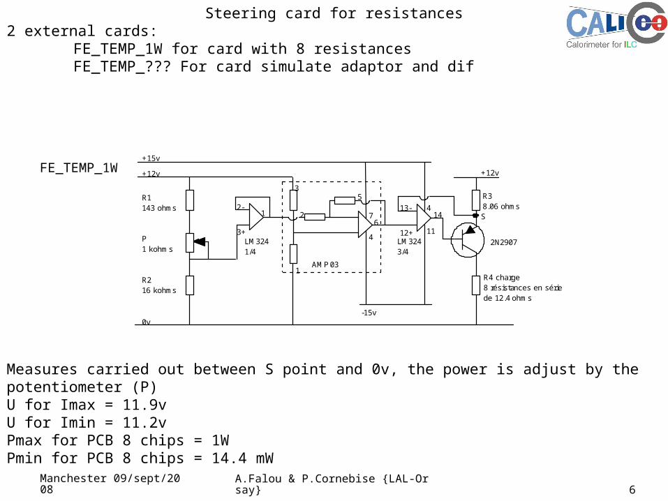
+12v+12v
+15v
0v
R1143 ohms
P1 kohms
R216 kohms
R4 charge8 résistances en série de 12.4 ohms
R38.06 ohms
2N290712+
13- 414
11LM3243/4
-15v
AMP03
3+
2-1
3
2
1
5
76
4
S
LM3241/4
Steering card for resistances2 external cards:
FE_TEMP_1W for card with 8 resistancesFE_TEMP_??? For card simulate adaptor and dif
Measures carried out between S point and 0v, the power is adjust by the potentiometer (P)U for Imax = 11.9vU for Imin = 11.2vPmax for PCB 8 chips = 1W Pmin for PCB 8 chips = 14.4 mW
FE_TEMP_1W

Manchester 09/sept/2008
A.Falou & P.Cornebise {LAL-Orsay} 7
Adaptor and dif card
1 card: FE_ADAPT_DIF2 parts:-Adaptor, with a square for 1 resistance and 1 gauge for temperature-Dif with 1 big resistance 1 pt100 for temperature
Dimensions:Thickness = 0.8 mm Width = 124.5 mm +0 -0.1 Length = 95 mm +0.1 -0.1
DIF CARD
ADAPTATOR CARD
FE_TEMP_43_44
PIN OUT CONNECTOR
Square forRESISTOR AND SENSOR
RESISTOR AND SENSOR
124 mm
40 mm
95 mm
49.5 mm
55 mm
74.5 mmoutsid
e the sla
bin sla
b
QUESTIONS : what are the values of the max power dissipated in the
adaptor part and dif part

Manchester 09/sept/2008
A.Falou & P.Cornebise {LAL-Orsay} 8
Resistance Gauge
Test and measurementA strain gauge Vishay (reference 183112 used as T° sensor) is glued on the PCB and the resistance which simulates the chip, is directly bonded to the gage.
Resistance glued to gauge
PT100 for calibration of the gauge
Steering resistance system
Temperature acquisition system

Manchester 09/sept/2008
A.Falou & P.Cornebise {LAL-Orsay} 9
Cards assembling in slab model
To achieve the interconnections between the PCBs, we use kapton combs
gauges S1 à S8resistances R1 à R8
gauge S12
gauge S13
gauge S14
gauge S15
gauge S16
38 wires
40 wires
42 wires
44 wires
46 wires
36 wires to the central acquisition
position 3 FE_TEMP_5_6gauge S11
6 wires
48 wires
position 4 FE_TEMP_17_48
position 5 FE_TEMP_7_8
position 6 FE_TEMP_9_10
position 7 FE_TEMP_11_12
position 8 FE_TEMP_13_14
position 9 FE_TEMP_15_16
18 wires to the steering card resistances
+1 2v+1 2v
+1 5v
0v
R1
14 3 oh ms
P1 k ohm s
R2
16 koh ms
R4 cha r ge8 r és is t anc es e n sé ri e
de 12. 4 o hms
R38. 0 6 oh m s
2N 22 1912 +
13 - 414
11LM 324
-15 v
AM P03
3+
2-1
3
2
1
5
76
4
s
s’
LM 324
FE_TEMP_1W
combs capton
position 2 FE_TEMP_3_4gauge S10
4 wires
position 1 FE_TEMP_1_2gauge S9
2 wires
Possibility to remove this cardon position 2-3-5-6-7-8-9
cooling
position 10 FE_ADAPT_DIF
56 wires
2 wires to the steering card resistances
+1 2v+1 2v
+1 5v
0v
R1
14 3 oh ms
P1 k ohm s
R2
16 koh ms
R4 cha r ge8 r és is t anc es e n sé ri e
de 12. 4 o hms
R38. 0 6 oh m s
2N 22 1912 +
13 - 414
11LM 324
-15 v
AM P03
3+
2-1
3
2
1
5
76
4
s
s’
LM 324
FE_TEMP_30W

Manchester 09/sept/2008
A.Falou & P.Cornebise {LAL-Orsay} 10
Step 1Comb 20 ways Kapton width = 19 mmWire = 0.25 mmTrack = 0.03 mm Wire + solder + track = moy 0.29 mm
Solder = moy 0.01 mm
Step 2Comb 32 ways Kapton width = 19 mmWire = 0.11 mmTrack = 0.03 mm Wire + solder + track = moy 0.15 mmSolder = moy 0.01 mm Step 3
Comb 20 ways Kapton width = 5 mmWire = 0.11 mmTrack = 0.03 mm Wire + solder + track = moy 0.15 mmSolder = moy 0.01 mmT max relieved on the top = 45.6 °C
T max relieved on the lower side wafers = 42.5 °C
Tests of kapton combs The combs are made by positioning the wires on a layer of kapton scotch and covered by another layer of kapton scotch.Then the wire are solder alternately starting with wire n° 1 and n° 10, 20, 2, 11, 21…Soldering iron used: Weller ws50 at 350°CThe temperature is controlled step by step with PT100 placed on the top and on the bottom (wafers side)

Manchester 09/sept/2008
A.Falou & P.Cornebise {LAL-Orsay} 11
Resistors loadParameters Value parameter
Enclosure type 0805
Technologie Thin Film
Value of resistance 12,4Ω
Tolerance resistance ±0.1%
Rated power at 70 °C 0.1W
Temperature coefficient ±10 ppm/°C
Using temperature -55°C à +125°C
Power use 100 V (max.)
Tension overload 200 V (max.)
Length 2mm
Width 1,25mm
Resistance R3Parameters Value parameter
Enclosure type 0805
Technologie Thin Film
Value of resistance 8,06Ω
Tolerance resistance ±0.1%
Rated power at 70 °C 0.125W
Temperature coefficient ±10 ppm/°C
Using temperature -55°C à +125°C
Power use 100 V (max.)
Tension overload 200 V (max.)
Length 2mm
Width 1,25mm
R2= resistance 16K OHM 0.1% 10PPM 0805R1=143Ω resistance 0805 143R 0.1% 15PPM
Documents annexes Steering card for resistances
2N2907

Manchester 09/sept/2008
A.Falou & P.Cornebise {LAL-Orsay} 12
Analog Devices AMP03
LM324

Manchester 09/sept/2008
A.Falou & P.Cornebise {LAL-Orsay} 13
Creation of a special card for making combs60 mm
30 mm
130 mm
18 mm4 mm
1.6 mm
2 mm
4 wires l = 0.2 mm
hole diameter 0.6 mm
2 x 48 pads
5 mm
8 mm
single sidethinkness PCB = 16/10thinkness CU = 17.5 µ
0.5 mm

Manchester 09/sept/2008
A.Falou & P.Cornebise {LAL-Orsay} 14
Control temperatureGauge Vishay temperature Sensors
AcknowledgmentsA Thiebault to manage temperatures
M Quentin for carrying out the solder on the capton combsM Gaspard for the current generator
J Fleury for schemasD Cuisy for the CAO
M Lacroix