manaul r1_0.doc · web viewit is ideal for live visualization of documents or films and scanning of...
TRANSCRIPT
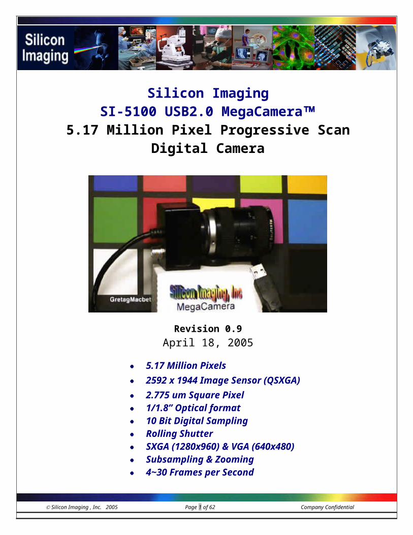
Silicon ImagingSI-5100 USB2.0 MegaCamera
5.17 Million Pixel Progressive Scan Digital Camera
Revision 0.9April 18, 2005
5.17 Million Pixels 2592 x 1944 Image Sensor (QSXGA)2.775 um Square Pixel1/1.8” Optical format10 Bit Digital Sampling Rolling ShutterSXGA (1280x960) & VGA (640x480)Subsampling & Zooming4~30 Frames per SecondRGB Bayer Color Auto White BalanceAuto Exposure ControlUSB2.0 Interface
**** Company Confidential ****
Silicon Imaging , Inc. 2005 Page 1 of 42 Company Confidential
SI-5100RGB MegaCamera™ 5.17 Megapixel, 10-Bit Digital USB 2.0 Smart Color Digital Camera
Silicon Imaging Inc.
Silicon Imaging , Inc. 2005 Page 2 of 42 Company Confidential
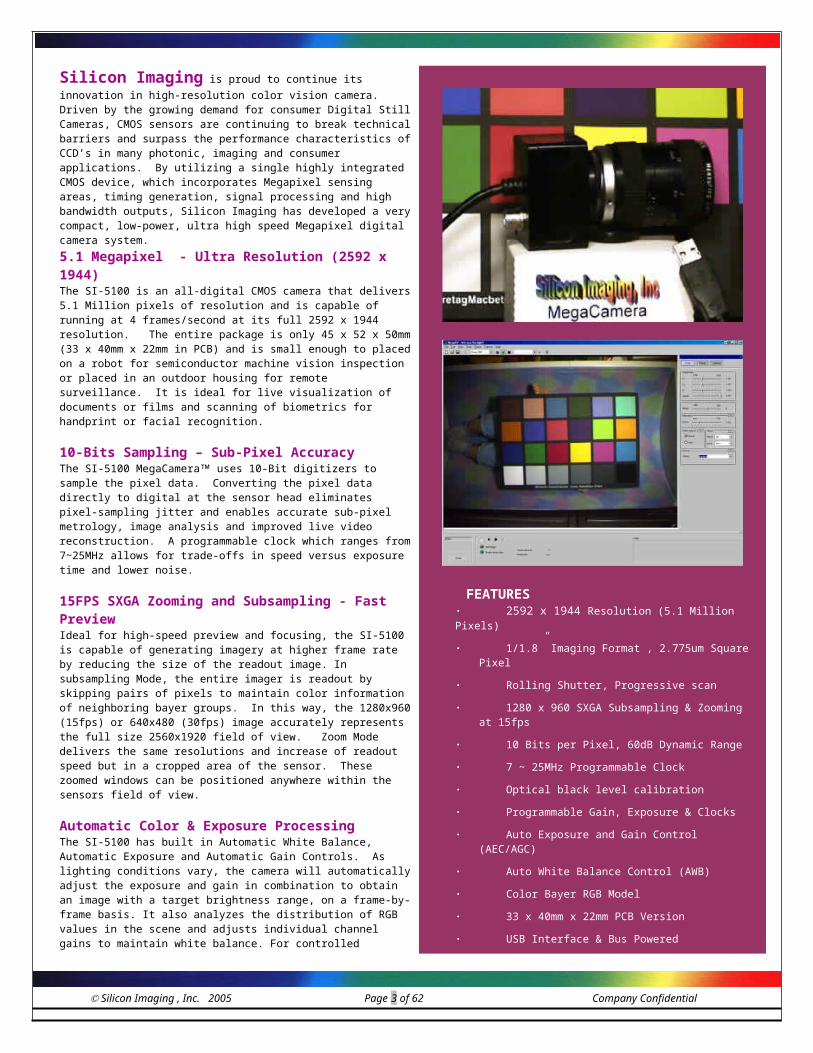
Silicon Imaging is proud to continue its innovation in high-resolution color vision camera. Driven by the growing demand for consumer Digital Still Cameras, CMOS sensors are continuing to break technical barriers and surpass the performance characteristics of CCD’s in many photonic, imaging and consumer applications. By utilizing a single highly integrated CMOS device, which incorporates Megapixel sensing areas, timing generation, signal processing and high bandwidth outputs, Silicon Imaging has developed a very compact, low-power, ultra high speed Megapixel digital camera system. 5.1 Megapixel - Ultra Resolution (2592 x 1944)The SI-5100 is an all-digital CMOS camera that delivers 5.1 Million pixels of resolution and is capable of running at 4 frames/second at its full 2592 x 1944 resolution. The entire package is only 45 x 52 x 50mm (33 x 40mm x 22mm in PCB) and is small enough to placed on a robot for semiconductor machine vision inspection or placed in an outdoor housing for remote surveillance. It is ideal for live visualization of documents or films and scanning of biometrics for handprint or facial recognition.
10-Bits Sampling – Sub-Pixel AccuracyThe SI-5100 MegaCamera uses 10-Bit digitizers to sample the pixel data. Converting the pixel data directly to digital at the sensor head eliminates pixel-sampling jitter and enables accurate sub-pixel metrology, image analysis and improved live video reconstruction. A programmable clock which ranges from 7~25MHz allows for trade-offs in speed versus exposure time and lower noise.
15FPS SXGA Zooming and Subsampling - Fast PreviewIdeal for high-speed preview and focusing, the SI-5100 is capable of generating imagery at higher frame rate by reducing the size of the readout image. In subsampling Mode, the entire imager is readout by skipping pairs of pixels to maintain color information of neighboring bayer groups. In this way, the 1280x960 (15fps) or 640x480 (30fps) image accurately represents the full size 2560x1920 field of view. Zoom Mode delivers the same resolutions and increase of readout speed but in a cropped area of the sensor. These zoomed windows can be positioned anywhere within the sensors field of view.
Automatic Color & Exposure Processing The SI-5100 has built in Automatic White Balance, Automatic Exposure and Automatic Gain Controls. As lighting conditions vary, the camera will automatically adjust the exposure and gain in combination to obtain an image with a target brightness range, on a frame-by-frame basis. It also analyzes the distribution of RGB values in the scene and adjusts individual channel gains to maintain white balance. For controlled lighting and inspection applications, gain and exposure values can be set manually via simple commands and software presets.
USB 2.0 High-Speed InterfaceThe high-speed image captures and connectivity is undergoing a revolution. The new UBS2.0 standard allows you to connect megapixel vision cameras with a single 4-wire cable directly into a 480Mbit/sec (megabits per second) port, found in every new motherboard produced with Intel P4 chipsets. These new USB 2.0 vision cameras can transfer precision 8 or 10-bit digital gray scale or color image data, eliminating the sampling jitter of traditional analog RS-170 systems. This interface also provides bi-directional serial communication for camera setup and control, triggering, strobing and other I/O signaling. One of the most convenient benefits is not requiring an additional power supply; these cameras are powered thru the same USB cable. For the vision system end-user, the benefit will be a lower system cost than previous camera and frame grabber solutions and plug-n-play installation.
FEATURES· 2592 x 1944 Resolution (5.1 Million Pixels)
· 1/1.8” Imaging Format , 2.775um Square Pixel
· Rolling Shutter, Progressive scan
· 1280 x 960 SXGA Subsampling & Zooming at 15fps
· 10 Bits per Pixel, 60dB Dynamic Range
· 7 ~ 25MHz Programmable Clock
· Optical black level calibration
· Programmable Gain, Exposure & Clocks
· Auto Exposure and Gain Control (AEC/AGC)
· Auto White Balance Control (AWB)
· Color Bayer RGB Model
· 33 x 40mm x 22mm PCB Version
· USB Interface & Bus Powered
· C-Mount Precision Machined Housing
SI-5100 USB2.0 MegaCamera Specifications
Silicon Imaging , Inc. 2005 Page 3 of 42 Company Confidential

Sensor: Optical Imaging Format 1/1.8” (7.33mm x 5.44mm)Active Pixels 2592H x 1944VPixel Size (pitch) 2.775 µm x 2.775 µm Pixel Type CMOS Aspect Ratio 1 : 1Spectral Response 350 ~ 1100 nmReadout Method Progressive ScanBlack Level Auto Black Level CalibrationShutter Rolling Shutter Shutter Speed Variable, 1 to 1998 row times Windowing (ROI) Horizontal & Vertical, No Speed-upSubsampling SXGA, VGA, HF ModesSubsampling & Zoom 1280 x 960 (SXGA)
640 x 480 (VGA)320 x 200 (HF)
Dynamic range 60 dB (10-bit ADC Conversion)Global Gain 1 to 8X, min step size 0.125Red/Blue Gains 1/3-X to 3-X Horizontal Blanking 408(QSXGA), 352(SXGA), 176(VGA) Minimum Row Time 3000 Clocks (2592+ 408 Blanking)Vertical Blanking 56 Rows Row/Frame Time 3000 clocks/row x 2000rows = 4fps
ADC & Digital Video OutputA/D Conversion Nominal 25Mhz (4fps @ 5.1MP)Vertical Resolution 10 Bit Readout Format 8-bit or 16bit (10-bit data)Readout Rate 7 ~ 25Mhz ( 8-bit format)
7 ~ 20Mhz (16-bit format)Max Transfer Rate ~ 40MB/sec (ICH4 or higher)Max Frame Rate
2592 x 19441280 x 960640 x 480
25MHz4
1530
15MHz2.59
20
USB2.0 High-Speed Interface & Control: USB Speed 480Mb/sec (High-Speed)Serial Communication Endpoint 0, Vendor ProtocolData Interface Endpoint 2, 2K FIFOProgrammable Modes Exposure, Gain, Windowing, Zoom
Mode & Window Subsampling, Clock rates
Region-of–Interest Programmable Horiz & VerticalAuto Gain Controls(AGC)
Manual / Automatic Global & Red/Blue
Auto White Balance (AWB)
Manual / Automatic AWB Threshold, AWB Speed
Auto Exposure Control (AEC)
Manual / AutomaticAEC Target Min/MaxAEC Speed/Steps
Histogram Counters R/Gr/Gb/B Channel AverageLuminance Average
Setting Timing Next top of FrameExternal Triggers (optional)
TTL Trigger-In / Strobe-Out w/3-Pin connection (option)
PowerInput Voltage +5 VDC +/- 10% < 500mAPower Consumption 2.0 WattsTrigger Connection (opt) Tajimi RO3-PB3M 3Pin (optional)Connection USB Bus Powered
MechanicalLens Mount C-Mount, 7mm Back focus Adj.Enclosure Size 45mm W x 52mm H x 50mm LWeight 8.5 oz. / 240gCamera Mount ¼” x 20 standard tripod mountCable Connector USB-A Cable Integrated
Spectral Response Curve
SI-5100 Ordering InformationSI-5100RGB-U 5.1 Megapixel USB2.0 Camera, RGB= Bayer Color -PCB PCB (33x40mm) Version of Camera. No housing included. -T External Trigger & strobe with 3-Pin Connection and Trigger/Strobe Breakout CableSDK Software Development Kit (Microsoft .NETSample Code, IPP Color Processing API & USB Capture
Silicon Imaging , Inc. 2005 Page 4 of 42 Company Confidential

Camera Architecture OverviewThe MegaCamera SI-5100 consists of 6 major component sections, which are built on two circuit boards.
1.) 5.17 Megapixel Sensor2.) Digital Clock Synthesizer3.) Digital Control Logic4.) Microprocessor5.) USB Interface6.) Power Regulation
SI-5100 Camera Block Diagram
1.) 5.17 Megapixel CMOS Image Sensor (2592 x 1944)
The MegaCamera SI-5100 utilizes a proprietary 5.17 Million pixel high-speed CMOS image sensor. Of the 5,174,400 pixels, 5,153,280 are active. The other pixels are used for black level calibration and interpolation. Each pixel is 2.775um square, ideal for image processing, and the entire array fits the 1/1.8” format for flexible optic choices. This reduction in process geometry allows for both an increase in transistors and fill factor without compromising performance, plus offers more advanced readout controls, greater speeds and lower power dissipation.
This new sensor technology offers a more responsive pixel design with added circuitry for increased dynamic range, greater sensitivity, decreased fixed pattern noise and low dark current for long exposure applications. Unlike CCD, which leak charge to adjacent pixels when the registers overflows (blooms), the SI-5100 provides inherent anti-blooming protection in each pixel, so that there is no blooming.
Silicon Imaging , Inc. 2005 Page 5 of 42 Company Confidential

The array has 2592 pixels on a line and 1944 active rows, which result in approx 3:4 aspect ratio. The sensor array design is based on a field integration read-out system with line-by-line transfer and an electronic shutter with a synchronous pixel read-out scheme (aka. Rolling Shutter Method).
Timing Generator (ROI Windowing, Subsampling & Zooming/Pan)
Various size images can be captured from the SI-5100. A Windowing Mode allows the selection of a portion of the full size imager to be transferred to the host. However, modifying window size or window position does not alter the frame or pixel rate. The Subsampling mode does allows faster readout of the entire field of view by doing by reading out 2 pixels and skipping 2 (4:2) in both horizontal and vertical directions. Using a window of 2560x1920, two subsampling modes can be obtained: SXGA (1280x960) with up to 15fps and VGA (640 x 480) at up to 30fps. A Zoom Mode provides the same SXGA and VGA resolutions and fps, but are cropped (zoomed) areas of the imager. The zoom position is programmable.
Analog Gain Amplifier (AGC) & Color Balance (AWB)
When the column sample/hold circuit has sampled one row of pixels, the pixel data will shift out one-by-one thruan analog amplifier with Global Gain. The amplifier gain can either be manually programmed by the user or controlled by the internal automatic gain control circuit (AGC). The adjustment range is 0 to 42 dB. The amplified signals are then color balanced with a channel balance block. In this block, the Red/Blue channel gain is increased or decreased to match Green channel luminance level along with gamma correction. The adjustment range is +/-9.5 dB. Red/Blue Channel Balance can be done manually by the user or by the internal automatic white balance (AWB) controller.
10-Bit A/D Conversion
The balanced signal is then digitized by the on-chip 10-bit ADC. It can operate at 40 MHz and is fully synchronous tothe pixel clock. The actual conversion rate is determined by the programmable clock rate.
Black Level Compensation
After the pixel data has been digitized, black level calibration can be applied before the data is output. The black level calibration block subtracts the average signal level of optical black pixels to compensate for the temperature and exposure time generated dark current in the pixel output. The user can disable black level calibration.
Bayer Digital Output (BG/GR)
The color balanced and black level corrected data is output from the sensor in 10-bit raw BG/GR Bayer Digital format and fed through the programmable logic to the USB2.0 High-Speed Interface either in 8-Bit (MSB) or16-bit mode.
Silicon Imaging , Inc. 2005 Page 6 of 42 Company Confidential

2.) 10-Bit Digital Sampling System A 10-Bit Analog-to-digital (A/D) converter samples each pixel value and quantizes it into 1024 levels inside the sensor. Pixel clock sampling ensures precise measurement of the photonic charge without the jitter and sampling uncertainty associated with traditional analog video systems, such as RS-170 and CCIR. The produces images which can deliver improved photometry accuracy and sub-pixel metrology. The use of 10-bit converters versus traditional 8-bit systems further enhances the image dynamic range. The combination of 10-bit vertical resolution and pixel clock sampling provide precise sub-pixel measurement accuracy (ex. 1/10 pixel).
3.) Digital Clock Synthesizer A wide range a master clock frequencies (eg. 7 to 25MHz) can by precisely generated using the Digital Clock Synthesizer. The frequency of the clock synthesizer can be set by vendor command. A table with associated clock frequency is found in the serial programming section of the manual. Due to frequency restriction on the digital transmission link and processor clocks, the pixel clock frequency cannot be lower than 5Mhz or higher than 25MHz. In 10-bit mode, the sustained data rate on the USB2.0 is up 2x the pixel clock rate. In order to maintain full 10-bit resolution the clock rate needs to be reduced to half the maximum. Alternatively, the camera is capable of switching to 8-bit mode and the clock rates increased.
4.) Embedded MicroprocessorA microprocessor in the camera provides the control interface between the PC and the functional block in the camera (Sensor, Clock Synthesizer, Register Memory, triggers & USB Interface. The Microprocessor receives commands thru the USB interface and issues commands to the other internal devices. It also can store preset values for camera setting, which can be recalled.
5.) USB2.0 Interface & PowerThe UBS2.0 interface connects the camera to the PC with a single 4-wire cable. The port provides sustained data rates of over 40MB/sec and also provides +5VDC to the camera for operation. The interface also provides bi-directional serial communication for camera setup and control, triggering, strobing and other I/O signaling.
PCB OEM Version 44 x 33 x 14mm - 2PCB Actual size
6.) Camera Control Signals & PowerSeveral digital I/O and power signals are available on the processor from PCB header points for custom OEM applications.
Silicon Imaging , Inc. 2005 Page 7 of 42 Company Confidential

InstallationDownload and install the current software from the Zip compressed file by double-clicking on the MegaXVInstall:
The Wizard will take you thru the steps to completion.
Once the MegaXV software and USB drivers (ezusb.sys & ezusbsi.inf) or extracted, you are ready to plug-in the camera.
Silicon Imaging , Inc. 2005 Page 8 of 42 Company Confidential

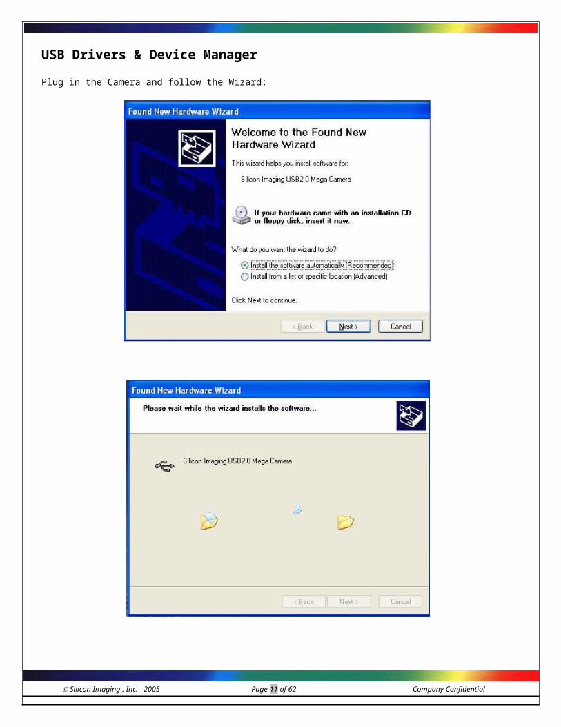
USB Drivers & Device ManagerPlug in the Camera and follow the Wizard:
Silicon Imaging , Inc. 2005 Page 9 of 42 Company Confidential

A warning message will appear:
Press Continue Anyway.
Select ‘Finish’. The Registry has now been updated and the camera can now be accessed by the MegaXV application.
Silicon Imaging , Inc. 2005 Page 10 of 42 Company Confidential
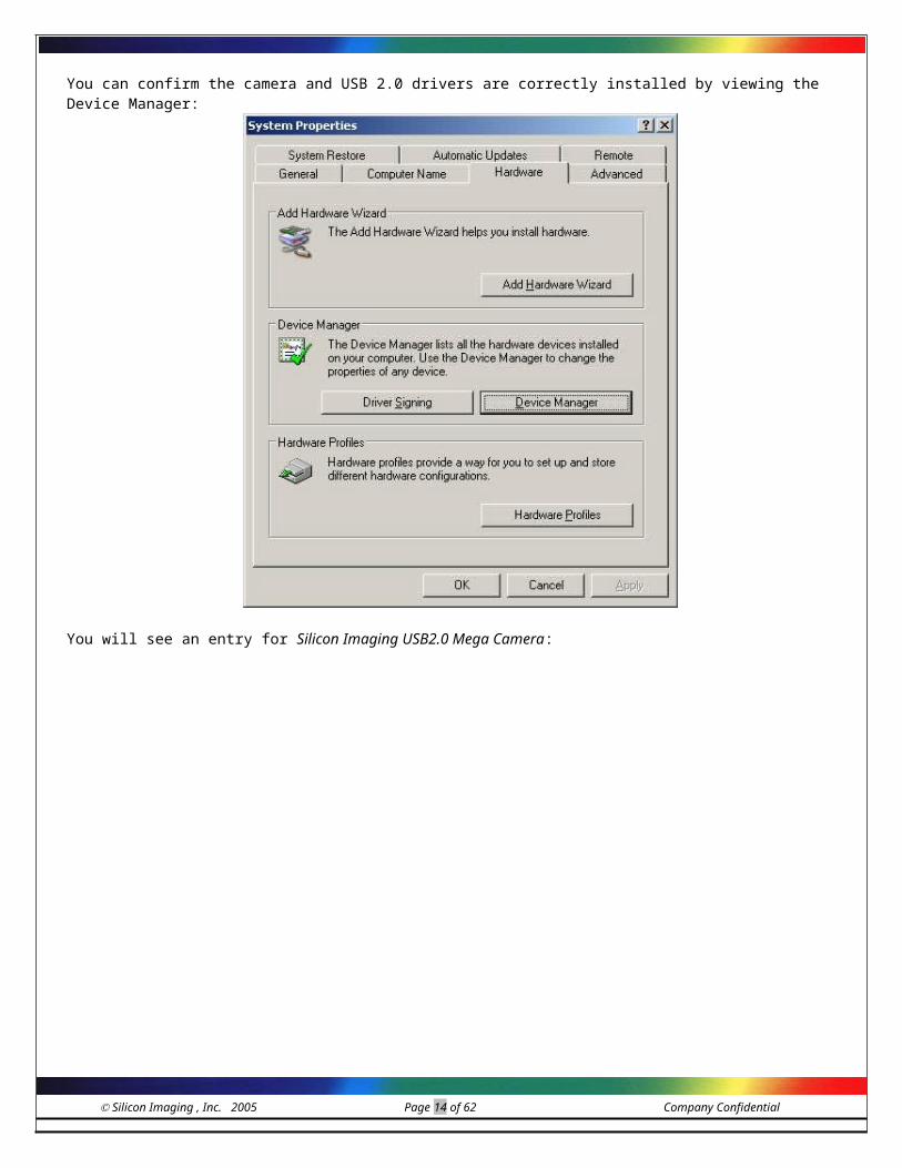
You can confirm the camera and USB 2.0 drivers are correctly installed by viewing the Device Manager:
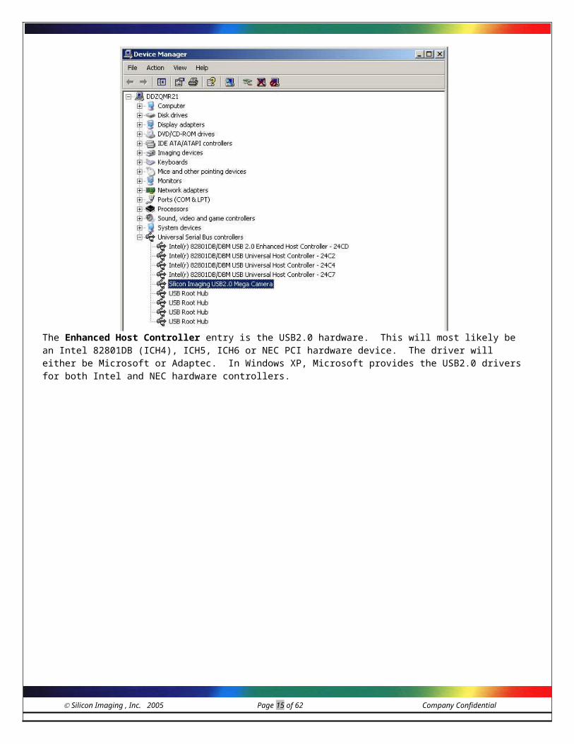
You will see an entry for Silicon Imaging USB2.0 Mega Camera:
Silicon Imaging , Inc. 2005 Page 11 of 42 Company Confidential

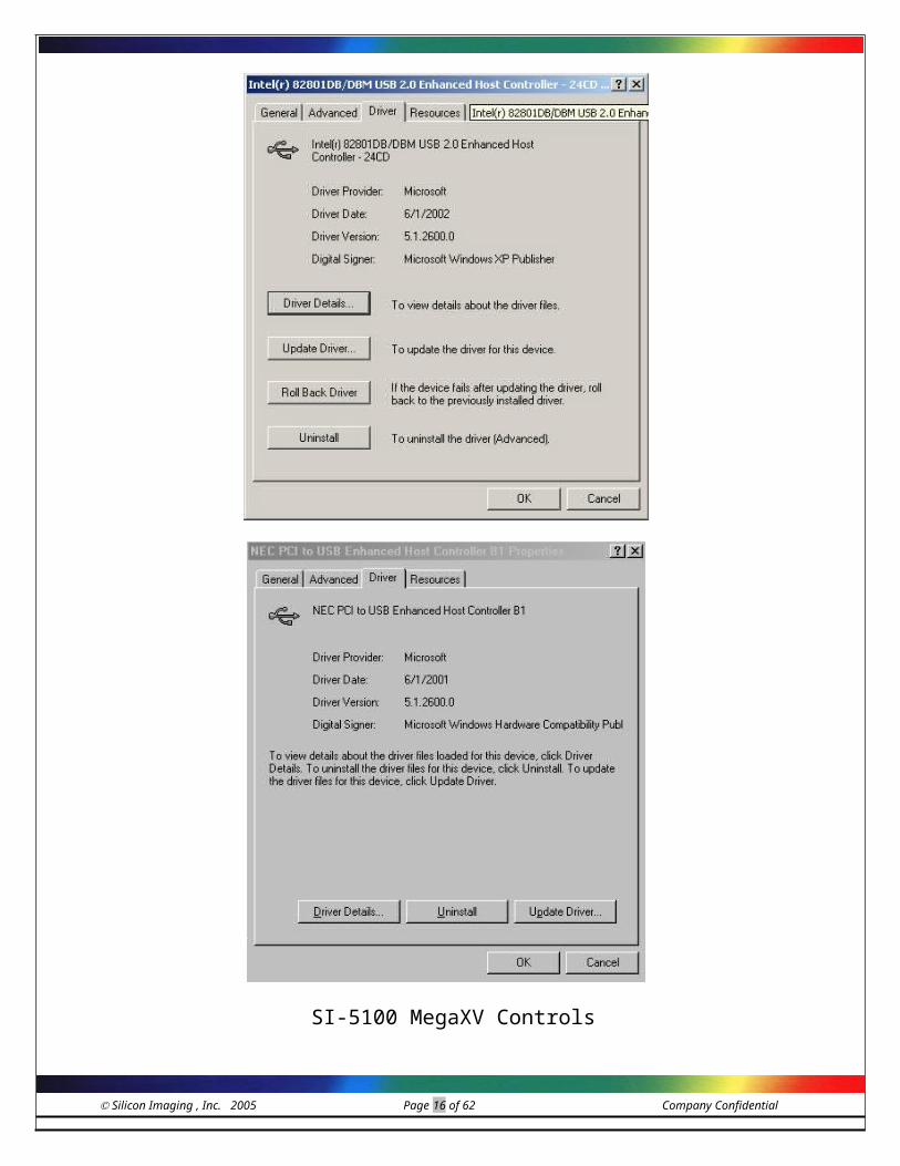
The Enhanced Host Controller entry is the USB2.0 hardware. This will most likely be an Intel 82801DB (ICH4), ICH5, ICH6 or NEC PCI hardware device. The driver will either be Microsoft or Adaptec. In Windows XP, Microsoft provides the USB2.0 drivers for both Intel and NEC hardware controllers.
Silicon Imaging , Inc. 2005 Page 12 of 42 Company Confidential

SI-5100 MegaXV Controls
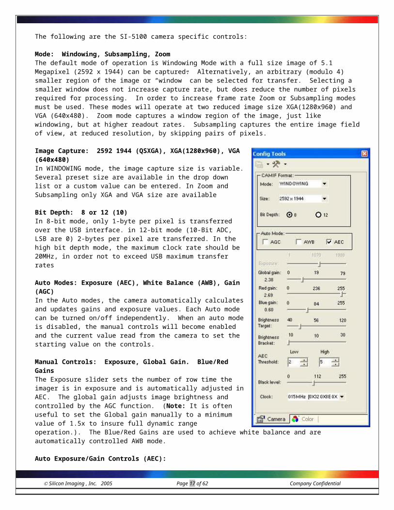
The following are the SI-5100 camera specific controls:
Mode: Windowing, Subsampling, ZoomThe default mode of operation is Windowing Mode with a full size image of 5.1 Megapixel (2592 x 1944) can be captured. Alternatively, an arbitrary (modulo 4) smaller region of the image or “window” can be selected for transfer. Selecting a smaller window does not increase capture rate, but does reduce the number of pixels required for processing. In order to increase frame rate Zoom or Subsampling modes must be used. These modes will operate at two reduced image size XGA(1280x960) and VGA (640x480). Zoom mode captures a window region of the image, just like windowing, but at higher readout rates. Subsampling captures the entire image field of view, at reduced resolution, by skipping pairs of pixels.
Image Capture: 2592 1944 (QSXGA), XGA(1280x960), VGA (640x480)In WINDOWING mode, the image capture size is variable. Several preset size are available in the drop down list or a custom value can be entered. In Zoom and Subsampling only XGA and VGA size are available
Bit Depth: 8 or 12 (10)In 8-bit mode, only 1-byte per pixel is transferred over the USB interface. in 12-bit mode (10-Bit ADC, LSB are 0) 2-bytes per pixel are transferred. In the high bit depth mode, the maximum clock rate should be 20MHz, in order not to exceed USB maximum transfer rates
Auto Modes: Exposure (AEC), White Balance (AWB), Gain (AGC)In the Auto modes, the camera automatically calculates and updates gains and exposure values. Each Auto mode can be turned on/off independently. When an auto mode is disabled, the manual controls will become enabled and the current value read from the camera to set the starting value on the controls.
Manual Controls: Exposure, Global Gain. Blue/Red GainsThe Exposure slider sets the number of row time the imager is in exposure and is automatically adjusted in AEC. The global gain adjusts image brightness and controlled by the AGC function. (Note: It is often useful to set the Global gain manually to a minimum value of 1.5x to insure full dynamic range operation.). The Blue/Red Gains are used to achieve white balance and are automatically controlled AWB mode.
Auto Exposure/Gain Controls (AEC): Brightness Target, Brightness BracketAEC threshold: Threshold low/high
The AEC/AGC function will automatically adjust exposure and gains to achieve a brightness target within the bracket range. If the average brightness is out of the AEC low/high threshold range, larger step changes of gain and exposure are applied.
Black Level Offset Use the Black level to adjust image offset and insure the signal output in black is above zero. This value may need to be adjusted for optimal operation at different gain settings.
Clock: 7~ 25MHz ProgrammableThe clock rate determines the readout speed of the camera over the USB bus and determines the maximum frame rate of the system. The nominal speed is 15MHz. For 10-bit (12) operation, the maximum rate should not exceed 20MHz, as the burst rate on the USB becomes 40MB/sec. Higher clock speeds also show increased FPN.
Silicon Imaging , Inc. 2005 Page 13 of 42 Company Confidential
Introduction to USB Communication
Vendor Requests – Endpoint-0 Communication
All camera controls and programming are done at the lowest level USB communication using Vendor Requests (VR). The VR’s codes have been assigned by Silicon Imaging, “the vendor” and their functions are defined in the following section.
The Vendor Request can be used to change all camera settings or the high-level API can be used to perform the same functions. The INFO-tab of MegaXV, provides a convenient method for sending these commands and seeing the results.
The basic Vendor Request provides the following fields:
Vendor Code: 8 bitsValue: 16 bitsIndex: 16 bitsLength: 16 bitsDirection: 1 bit, (IN (1) or OUT (0))
A non-zero length vendor request implies an endpoint 0 (EP0) data transfer, which is either IN or OUT. A "Hex Bytes" input field is provided in the control panel window and holds the data for OUT transfers.
TransferCamControlData( )
The following is the Silicon Imaging API function used to send any vendor request command:
int TransferCamControlData (int iCamNumber, int iVendorRequestCode, int iIndex, int iValue, int iDirection, int iBufferSize, unsigned char* buffer) ;
Description:
Downloads or uploads arbitrary Endpoint-0 control data to the camera registers.
Arguments:
iCamNumber – number of camera deviceiVendorRequestCode - vendor request codeiIndex – Camera register or value (16 bits)iValue – data value per command (16 bits)iDirection – 1 (IN) - transmit commands with return string from camera
0 (OUT) - download from host to camera with host providing stringiBufferSize – number of bytes to transfer to/from register specified by the iIndex value*buffer – pointer to buffer containing control information (typ recived from the camera for 1=IN)
A non-zero Length Vendor Request implies an EndPoint 0 (EP0) data transfer, which is either IN or OUT.
Silicon Imaging , Inc. 2005 Page 14 of 42 Company Confidential
SI-5100 LOW LEVEL USB VENDOR CODES
VR Function Value Index DIR Buffer Description
0xD1 Write Register xVVVV
Value toWrite
xRRRR
RegisterTo Write
1 0No data response.
0xD0 Read Register 0 xRRRegister 1 1 Read Register (8-bit) response
0xE1 Read Firmware Version 0 0 1 16 Issue an IN transfer of Length 16 to Read
Firmware Version. The Value and Index fields are ignored. The returned string will contain ASCII characters, and the last byte will be zero.
0xE7 Read Serial Number 0 0 1 16 To read Serial Number String from the Camera, issue an IN transfer of Length 16 bytes. The Value and Index fields are ignored. The returned string will contain ASCII characters.
0xE4 Write Flash memory (OUT) 0 0x0000to
0x00FF
0 32 An OUT transfer of 16 is used for storage of 32 words of 14bit values. The Index field is used to address 256 blocks(0xFF) of memory. The first byte and every odd byte contain only 6 usable bits. The Value field is ignored. This command is used in firmware upgrades, but the data storage can be used for other function
0xE4 Read Flash memory(OUT)Note: This memory space is used in firmware upgrades and will overwrite any user data stored in this memory.
0 0x0000 -
0x00FF
1 32 An IN transfer of 32 is used to read 16 words of 14bit values. The Index field is used to address 256 blocks (0xFF) of memory. The first byte and every odd byte contain only 6 usable bits. The Value field is ignored. This command is read arbitrary data stored by the Write Flash command.
0xE4 Upgrade Firmware (IN)
WARNING! Please wait 30 seconds before unplugging the camera to allow the upgrade to complete.
CODE 0 1 4 An IN request of Length 4 will expect a firmware upgrade code (from factory) in the Value field (length 16 bits – 4 hex). Index field ignored. If the CODE does not match, the returned 4 bytes will contain the ASCII "FAIL". If the code does match, the 4 bytes of data returned will be "DONE". After the firmware update is done, the USB Camera should be reboot (unplug and replug). The new firmware will then be active.
0xE8 Read CPLD code 0 0 1 4 An IN transfers of Length 4 bytes will return the CPLD Firmware Code.
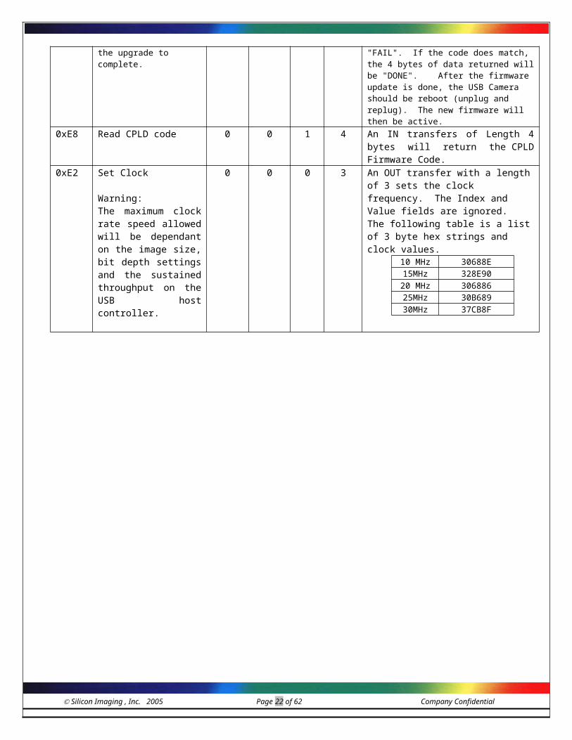
0xE2 Set Clock
Warning:The maximum clock rate speed allowed will be dependant on the image size, bit depth settings and the sustained throughput on the USB host controller.
0 0 0 3 An OUT transfer with a length of 3 sets the clock frequency. The Index and Value fields are ignored. The following table is a list of 3 byte hex strings and clock values.
10 MHz 30688E15MHz 328E9020 MHz 30688625MHz 30B68930MHz 37CB8F
Silicon Imaging , Inc. 2005 Page 15 of 42 Company Confidential
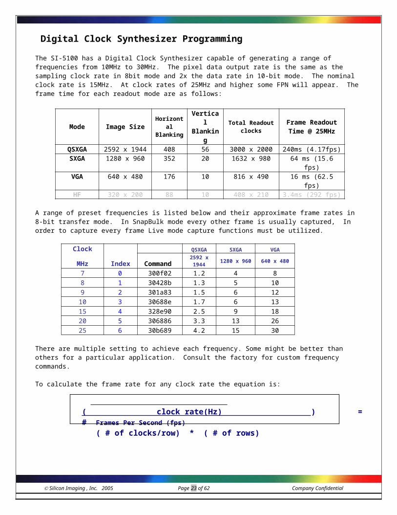
Digital Clock Synthesizer ProgrammingThe SI-5100 has a Digital Clock Synthesizer capable of generating a range of frequencies from 10MHz to 30MHz. The pixel data output rate is the same as the sampling clock rate in 8bit mode and 2x the data rate in 10-bit mode. The nominal clock rate is 15MHz. At clock rates of 25MHz and higher some FPN will appear. The frame time for each readout mode are as follows:
Mode Image Size Horizontal Blanking
Vertical Blanking
Total Readoutclocks
Frame ReadoutTime @ 25MHz
QSXGA 2592 x 1944 408 56 3000 x 2000 240ms (4.17fps)SXGA 1280 x 960 352 20 1632 x 980 64 ms (15.6 fps)VGA 640 x 480 176 10 816 x 490 16 ms (62.5 fps)HF 320 x 200 88 10 408 x 210 3.4ms (292 fps)
A range of preset frequencies is listed below and their approximate frame rates in 8-bit transfer mode. In SnapBulk mode every other frame is usually captured, In order to capture every frame Live mode capture functions must be utilized.
Clock QSXGA SXGA VGAMHz Index Command 2592 x 1944 1280 x 960 640 x 480
7 0 300f02 1.2 4 88 1 30428b 1.3 5 109 2 301a83 1.5 6 12
10 3 30688e 1.7 6 1315 4 328e90 2.5 9 1820 5 306886 3.3 13 2625 6 30b689 4.2 15 30
There are multiple setting to achieve each frequency. Some might be better than others for a particular application. Consult the factory for custom frequency commands.
To calculate the frame rate for any clock rate the equation is:
( clock rate(Hz) ) = # Frames Per Second (fps)
( # of clocks/row) * ( # of rows)
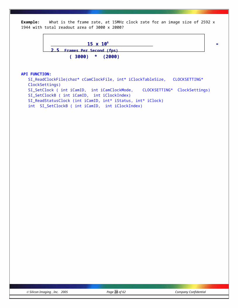
Example: What is the frame rate, at 15MHz clock rate for an image size of 2592 x 1944 with total readout area of 3000 x 2000?
15 x 10 6 = 2.5 Frames Per Second (fps) ( 3000) * (2000)
API FUNCTION:
SI_ReadClockFile(char* cCamClockFile, int* iClockTableSize, CLOCKSETTING* ClockSettings)SI_SetClock ( int iCamID, int iCamClockMode, CLOCKSETTING* ClockSettings)SI_SetClockB ( int iCamID, int iClockIndex)SI_ReadStatusClock (int iCamID, int* iStatus, int* iClock)int SI_SetClockB ( int iCamID, int iClockIndex)
Silicon Imaging , Inc. 2005 Page 16 of 42 Company Confidential
SI-5100 Sensor Register Programming
Image Size (Windowing, Subsampling & Zooming)The SI-5100 will default into the full 5.1Megapixel resolution image of 2592 x 1944. The image readout rate (frame rate) will depend on the camera clock speed. The display update rate will depend on the PC CPU speed and bayer color processing selections.
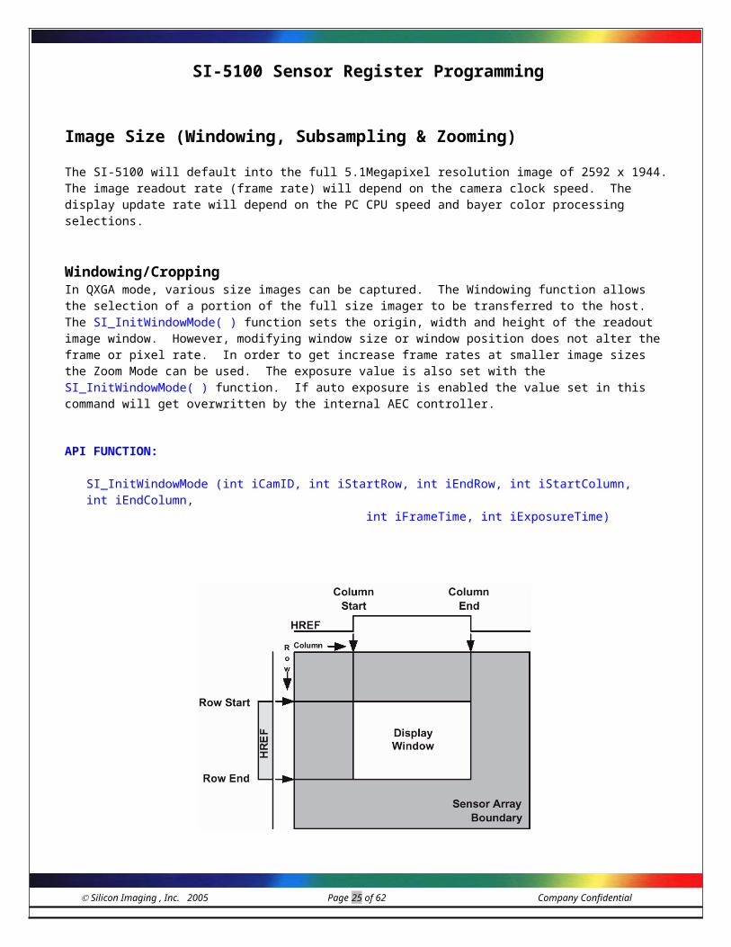
Windowing/CroppingIn QXGA mode, various size images can be captured. The Windowing function allows the selection of a portion of the full size imager to be transferred to the host. The SI_InitWindowMode( ) function sets the origin, width and height of the readout image window. However, modifying window size or window position does not alter the frame or pixel rate. In order to get increase frame rates at smaller image sizes the Zoom Mode can be used. The exposure value is also set with the SI_InitWindowMode( ) function. If auto exposure is enabled the value set in this command will get overwritten by the internal AEC controller.
API FUNCTION:
SI_InitWindowMode (int iCamID, int iStartRow, int iEndRow, int iStartColumn, int iEndColumn, int iFrameTime, int iExposureTime)
These API functions modify registers RES MODE, HREFST, HREFEND, VSTRT, VEND, and HREF_LSB to set the image size and window positioning.
Silicon Imaging , Inc. 2005 Page 17 of 42 Company Confidential
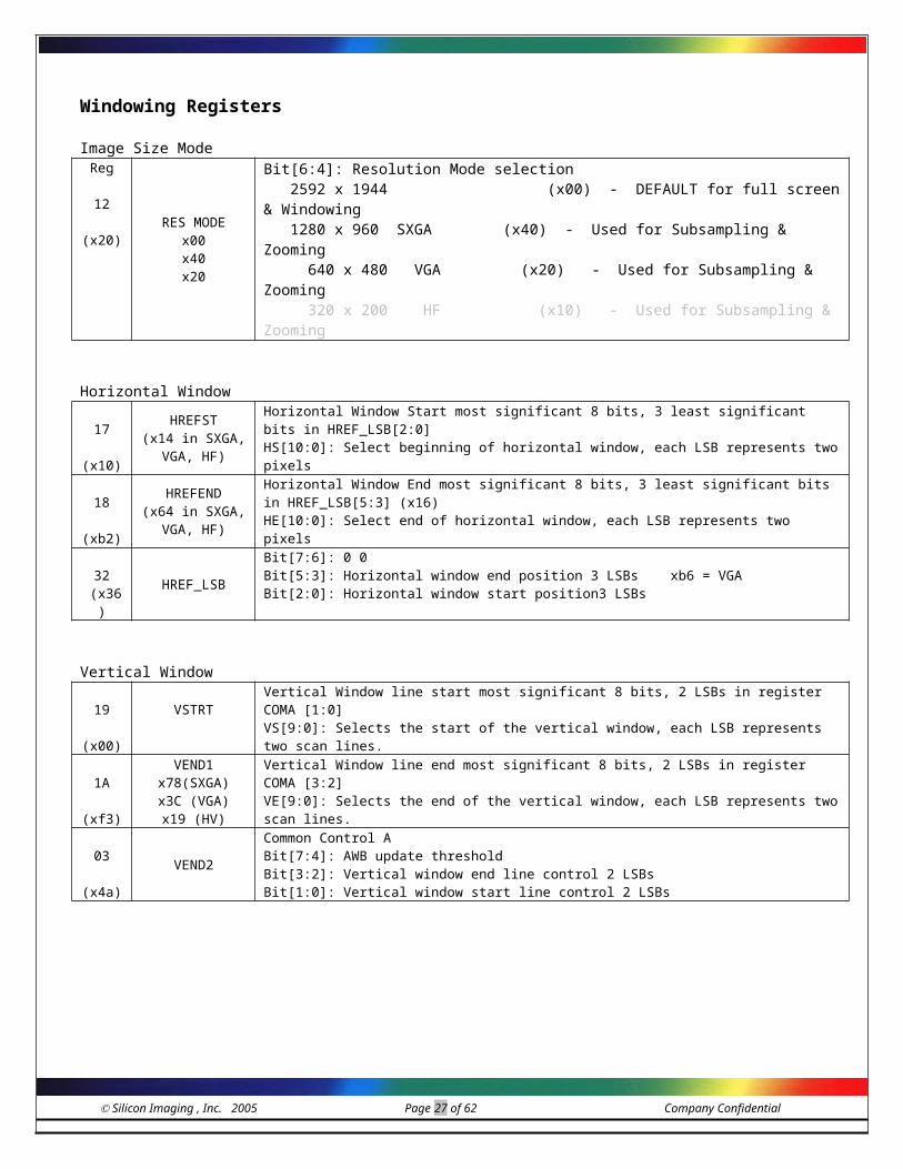
Windowing Registers
Image Size ModeReg
12
(x20)
RES MODEx00x40x20
Bit[6:4]: Resolution Mode selection 2592 x 1944 (x00) - DEFAULT for full screen & Windowing 1280 x 960 SXGA (x40) - Used for Subsampling & Zooming 640 x 480 VGA (x20) - Used for Subsampling & Zooming 320 x 200 HF (x10) - Used for Subsampling & Zooming
Horizontal Window
17
(x10)
HREFST(x14 in SXGA,
VGA, HF)
Horizontal Window Start most significant 8 bits, 3 least significant bits in HREF_LSB[2:0]HS[10:0]: Select beginning of horizontal window, each LSB represents two pixels
18
(xb2)
HREFEND(x64 in SXGA,
VGA, HF)
Horizontal Window End most significant 8 bits, 3 least significant bits in HREF_LSB[5:3] (x16)HE[10:0]: Select end of horizontal window, each LSB represents two pixels
32 (x36) HREF_LSB
Bit[7:6]: 0 0 Bit[5:3]: Horizontal window end position 3 LSBs xb6 = VGABit[2:0]: Horizontal window start position3 LSBs
Vertical Window
19
(x00)
VSTRT Vertical Window line start most significant 8 bits, 2 LSBs in register COMA [1:0]VS[9:0]: Selects the start of the vertical window, each LSB represents two scan lines.
1A
(xf3)
VEND1x78(SXGA)x3C (VGA)x19 (HV)
Vertical Window line end most significant 8 bits, 2 LSBs in register COMA [3:2]VE[9:0]: Selects the end of the vertical window, each LSB represents two scan lines.
03
(x4a)
VEND2
Common Control ABit[7:4]: AWB update thresholdBit[3:2]: Vertical window end line control 2 LSBsBit[1:0]: Vertical window start line control 2 LSBs
Silicon Imaging , Inc. 2005 Page 18 of 42 Company Confidential

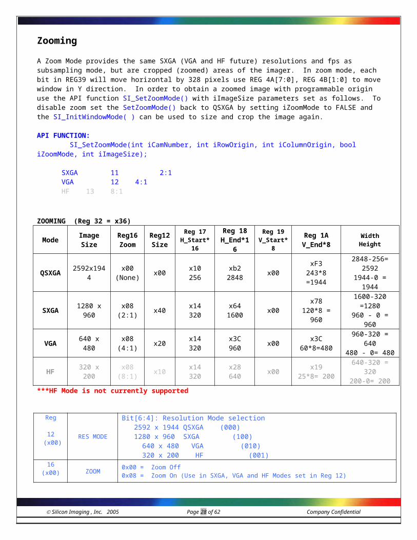
ZoomingA Zoom Mode provides the same SXGA (VGA and HF future) resolutions and fps as subsampling mode, but are cropped (zoomed) areas of the imager. In zoom mode, each bit in REG39 will move horizontal by 328 pixels use REG 4A[7:0], REG 4B[1:0] to move window in Y direction. In order to obtain a zoomed image with programmable origin use the API function SI_SetZoomMode() with iImageSize parameters set as follows. To disable zoom set the SetZoomMode() back to QSXGA by setting iZoomMode to FALSE and the SI_InitWindowMode( ) can be used to size and crop the image again.
API FUNCTION: SI_SetZoomMode(int iCamNumber, int iRowOrigin, int iColumnOrigin, bool iZoomMode, int iImageSize);
SXGA 11 2:1VGA 12 4:1HF 13 8:1
ZOOMING (Reg 32 = x36)
Mode Image Size
Reg16 Zoom
Reg12Size
Reg 17H_Start*16
Reg 18H_End*16
Reg 19V_Start*8
Reg 1AV_End*8
WidthHeight
QSXGA 2592x1944 x00(None) x00 x10
256xb2
2848 x00 xF3243*8 =1944
2848-256= 25921944-0 = 1944
SXGA 1280 x 960 x08(2:1) x40 x14
320x64
1600 x00 x78120*8 = 960
1600-320 =1280960 - 0 = 960
VGA 640 x 480 x08(4:1) x20 x14
320x3C960 x00 x3C
60*8=480960-320 = 640480 - 0= 480
HF 320 x 200 x08(8:1) x10 x14
320x28640 x00 x19
25*8= 200640-320 = 320
200-0= 200***HF Mode is not currently supported
Reg
12 (x00)
RES MODE
Bit[6:4]: Resolution Mode selection 2592 x 1944 QSXGA (000) 1280 x 960 SXGA (100) 640 x 480 VGA (010) 320 x 200 HF (001)
16(x00) ZOOM 0x00 = Zoom Off
0x08 = Zoom On (Use in SXGA, VGA and HF Modes set in Reg 12)
32 (x36) HREF_LSB
Bit[7:6]: 0 0 Bit[5:3]: Horizontal window end position 3 LSBs Bit[2:0]: Horizontal window start position3 LSBs
4A
(x00)V_ZOOM1 Zoom Mode Vertical Window Start Point 8 MSBs
4A
(x00)V_ZOOM1 Zoom Mode Vertical Window Start Point 8 MSBs
4B
(x00)V_ZOOM2
Zoom Mode Vertical Window Start Point Control 2 LSBBit[7:2]: ReservedBit[1:0]: Zoom mode vertical window start point LSB
Silicon Imaging , Inc. 2005 Page 19 of 42 Company Confidential

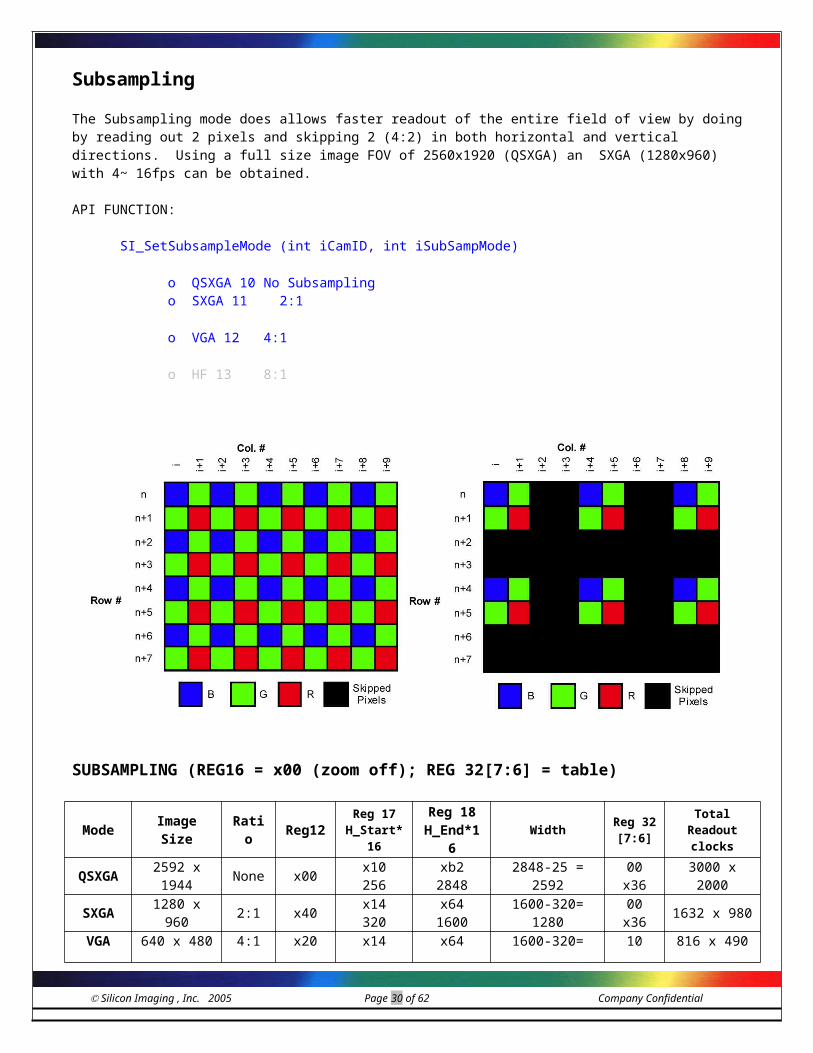
SubsamplingThe Subsampling mode does allows faster readout of the entire field of view by doing by reading out 2 pixels and skipping 2 (4:2) in both horizontal and vertical directions. Using a full size image FOV of 2560x1920 (QSXGA) an SXGA (1280x960) with 4~ 16fps can be obtained. API FUNCTION:
SI_SetSubsampleMode (int iCamID, int iSubSampMode)
o QSXGA 10 No Subsamplingo SXGA 11 2:1
o VGA 12 4:1
o HF 13 8:1
SUBSAMPLING (REG16 = x00 (zoom off); REG 32[7:6] = table)
Mode Image Size Ratio Reg12 Reg 17H_Start*16
Reg 18H_End*16 Width Reg 32
[7:6]Total Readout
clocks
QSXGA 2592 x 1944 None x00 x10256
xb22848 2848-25 = 2592 00
x36 3000 x 2000
SXGA 1280 x 960 2:1 x40 x14320
x641600 1600-320= 1280 00
x36 1632 x 980
VGA 640 x 480 4:1 x20 x14320
x641600
1600-320= 1280Skip2 (Reg32)
10xb6 816 x 490
HF 320 x 200 8:1 x10 x14320
x641600
1600-320= 1280Skip4 (Reg32)
11xf6 408 x 210
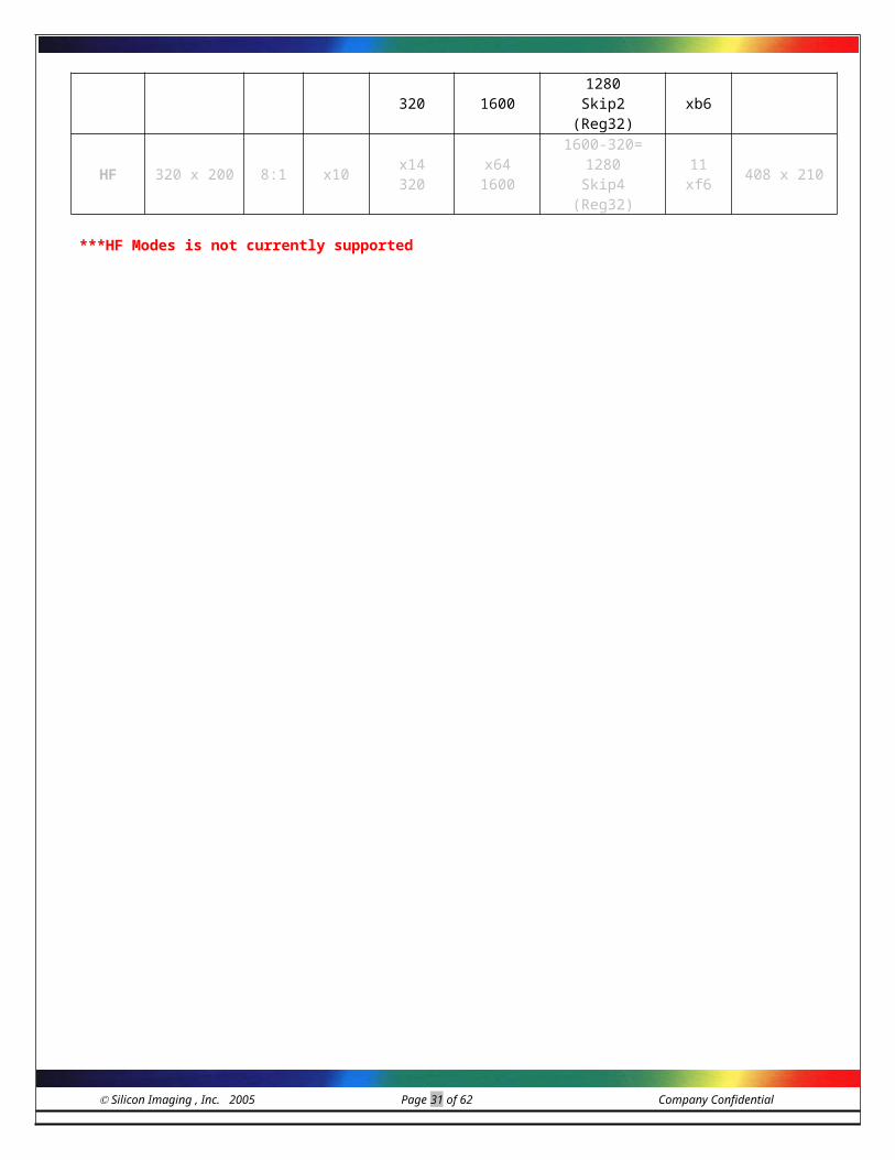
***HF Modes is not currently supported
Silicon Imaging , Inc. 2005 Page 20 of 42 Company Confidential

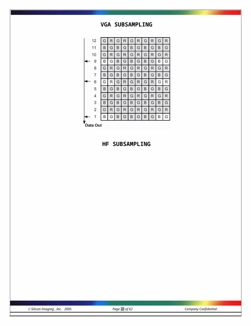
VGA SUBSAMPLING
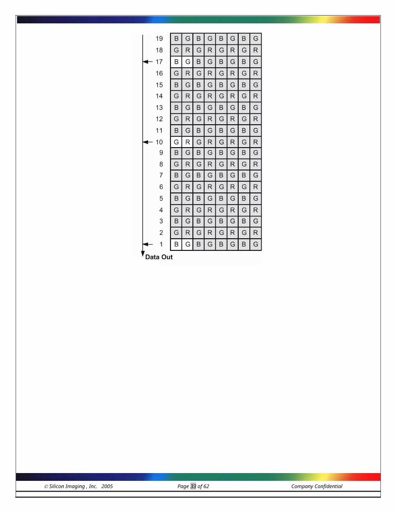
HF SUBSAMPLING
Silicon Imaging , Inc. 2005 Page 21 of 42 Company Confidential
Manual/ Auto Exposure/Gain Control (AEC/AGC) The SI-5100 camera exposure time can be controlled manually or automatically. Use SI_SetAutoMode( ) to select between Manual and Auto Mode. To disable auto updates to gain and exposure set the mode to MANUAL_EXP_GAIN.
Exposure Time = Exposure Register * Row_Time
To set the number of rows use SetExposureValue( ). The default range for QSXGA is 1 to 1998 row times. This value is 2 rows less than the readout rows. In order to extend exposure, the clock rate can be slowed or additional rows can be added to the readout by increasing vertical blanking using SI_SetVerticalBlanking. To program long exposure Reg 45 Bits[7:6] must be used to set the MSB of the exposure register.
Mode Image Size Total Readoutclocks
Max ExposureRows (No VB) Row Time Row Time
@ 15MhzRow Time@ 20MHz
Row Time@ 25MHz
QSXGA 2592 x 1944 3000 x 2000 1998 3000 * Pclk 200us 150us 120usSXGA 1280 x 960 1632 x 980 978 1632 * Pclk 109us 82us 65usVGA 640 x 480 816 x 490 488 816 * Pclk 54us 41us 33usHF 320 x 200 408 x 210 208 408 * Pclk 27us 20us 16us
API FUNCTION:
SI_SetAutoMode(int iCamID, int iMode) . iModes = 0 (MANUAL_EXP_GAIN)SI_SetExposureValue(int iCamNumber, int iExposure);SI_SetVerticalBlanking(int iCamNumber, int iVertBlanking);
13 (xC7) Auto/Manual
Exposure
0xC0 = Manual0xC5 = Auto Exposure Control / Auto Gain Control (AEC/AGC) or0xC7 = Auto White Balance & Exposure (AWB/AEC/AGC)
10 (x43) AEC[16:0]
Exposure[8 CSB]
Exposure Time = t LINE x AEC[16:0] AEC[16:11] = Reg45[5:0] = 6MSB (these bits are not current set by SetExposureValue() AEC[10:3 ] = Reg10[7:0] = 8CSB AEC [ 2:0 ] = Reg04[2:0] = 3LSB***Note: Max Exposure time is 1 Frame period even if AEC is set longer than frame perod.
45 (x00)
AEC_H[6 MSB]
Bit[7:6]: AGC[9:8} AGC highest gainBit[5:0]: AEC[16:11] Exposure value MSB
04 (x00)
AEC_L[3LSB]
Bit[7:3]: AWB Step Selection & Update Speed SelectionBit[2:0]: Exposure lower 3 bits – AEC[2:0]
24 (x40)
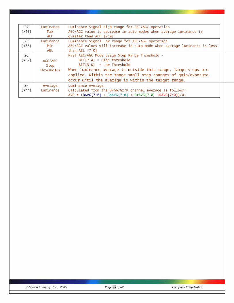
LuminanceMax AEH
Luminance Signal High range for AEC/AGC operationAEC/AGC value is decrease in auto modes when average luminance is greater than AEH [7:0]
25 (x30)
LuminanceMinAEL
Luminance Signal Low range for AEC/AGC operationAEC/AGC values will increase in auto mode when average luminance is less than AEL [7:0]
26(x52) AGC/AEC
Step Thresholds
Fast AEC/AGC Mode Large Step Range Threshold – BIT[7:4] = High threshold BIT[3:0] = Low ThresholdWhen luminance average is outside this range, large steps are applied. Within the range small step changes of gain/exposure occur until the average is within the target range.
2F (x00)
Average Luminance
Luminance AverageCalculated from the B/Gb/Gr/R channel average as follows:AVG = (BAVG[7:0] + GbAVG[7:0] + GrAVG[7:0] +RAVG[7:0])/4)
Silicon Imaging , Inc. 2005 Page 22 of 42 Company Confidential
Auto Exposure Control / Auto Gain Control (AEC/AGC)
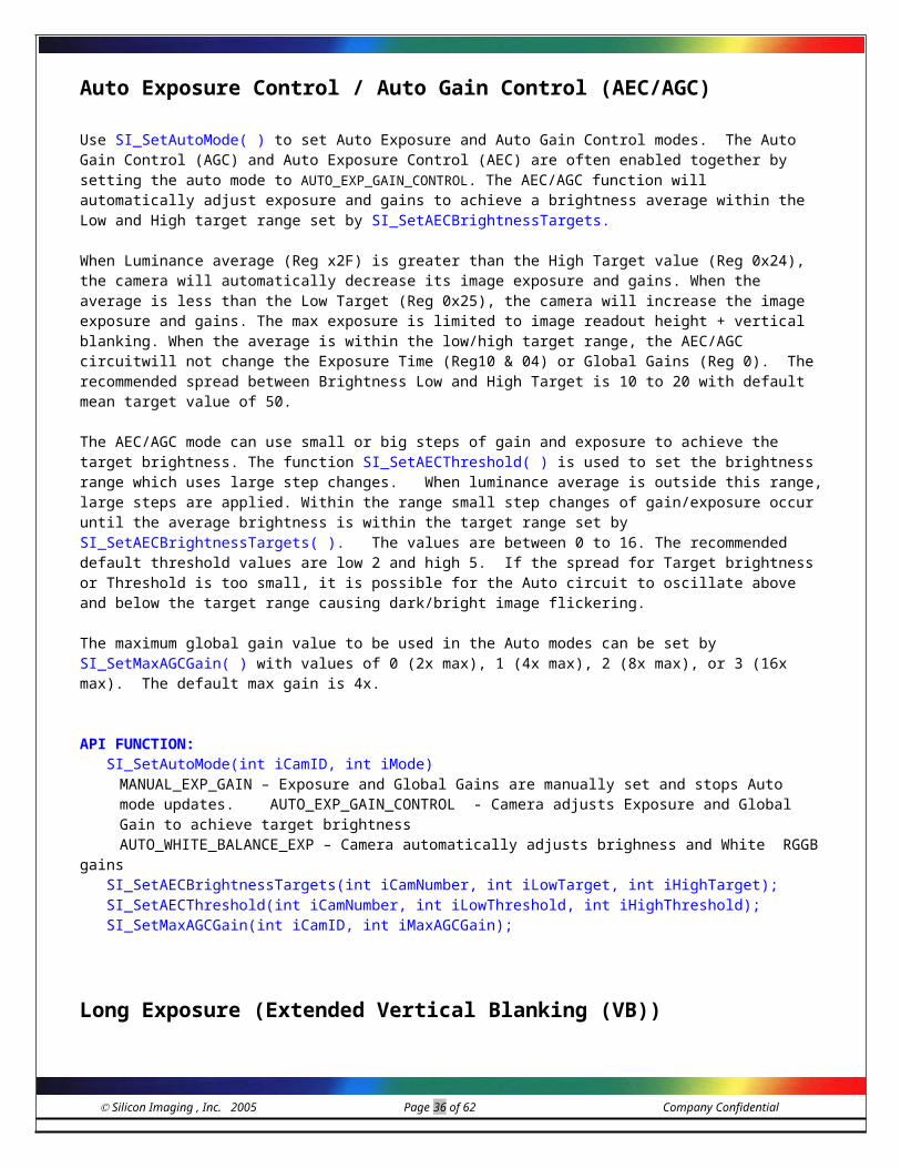
Use SI_SetAutoMode( ) to set Auto Exposure and Auto Gain Control modes. The Auto Gain Control (AGC) and Auto Exposure Control (AEC) are often enabled together by setting the auto mode to AUTO_EXP_GAIN_CONTROL. The AEC/AGC function will automatically adjust exposure and gains to achieve a brightness average within the Low and High target range set by SI_SetAECBrightnessTargets.
When Luminance average (Reg x2F) is greater than the High Target value (Reg 0x24), the camera will automatically decrease its image exposure and gains. When the average is less than the Low Target (Reg 0x25), the camera will increase the image exposure and gains. The max exposure is limited to image readout height + vertical blanking. When the average is within the low/high target range, the AEC/AGC circuitwill not change the Exposure Time (Reg10 & 04) or Global Gains (Reg 0). The recommended spread between Brightness Low and High Target is 10 to 20 with default mean target value of 50.
The AEC/AGC mode can use small or big steps of gain and exposure to achieve the target brightness. The function SI_SetAECThreshold( ) is used to set the brightness range which uses large step changes. When luminance average is outside this range, large steps are applied. Within the range small step changes of gain/exposure occur until the average brightness is within the target range set by SI_SetAECBrightnessTargets( ). The values are between 0 to 16. The recommended default threshold values are low 2 and high 5. If the spread for Target brightness or Threshold is too small, it is possible for the Auto circuit to oscillate above and below the target range causing dark/bright image flickering.
The maximum global gain value to be used in the Auto modes can be set by SI_SetMaxAGCGain( ) with values of 0 (2x max), 1 (4x max), 2 (8x max), or 3 (16x max). The default max gain is 4x.
API FUNCTION:SI_SetAutoMode(int iCamID, int iMode)
MANUAL_EXP_GAIN – Exposure and Global Gains are manually set and stops Auto mode updates. AUTO_EXP_GAIN_CONTROL - Camera adjusts Exposure and Global Gain to achieve target brightnessAUTO_WHITE_BALANCE_EXP – Camera automatically adjusts brighness and White RGGB gains
SI_SetAECBrightnessTargets(int iCamNumber, int iLowTarget, int iHighTarget);SI_SetAECThreshold(int iCamNumber, int iLowThreshold, int iHighThreshold);SI_SetMaxAGCGain(int iCamID, int iMaxAGCGain);
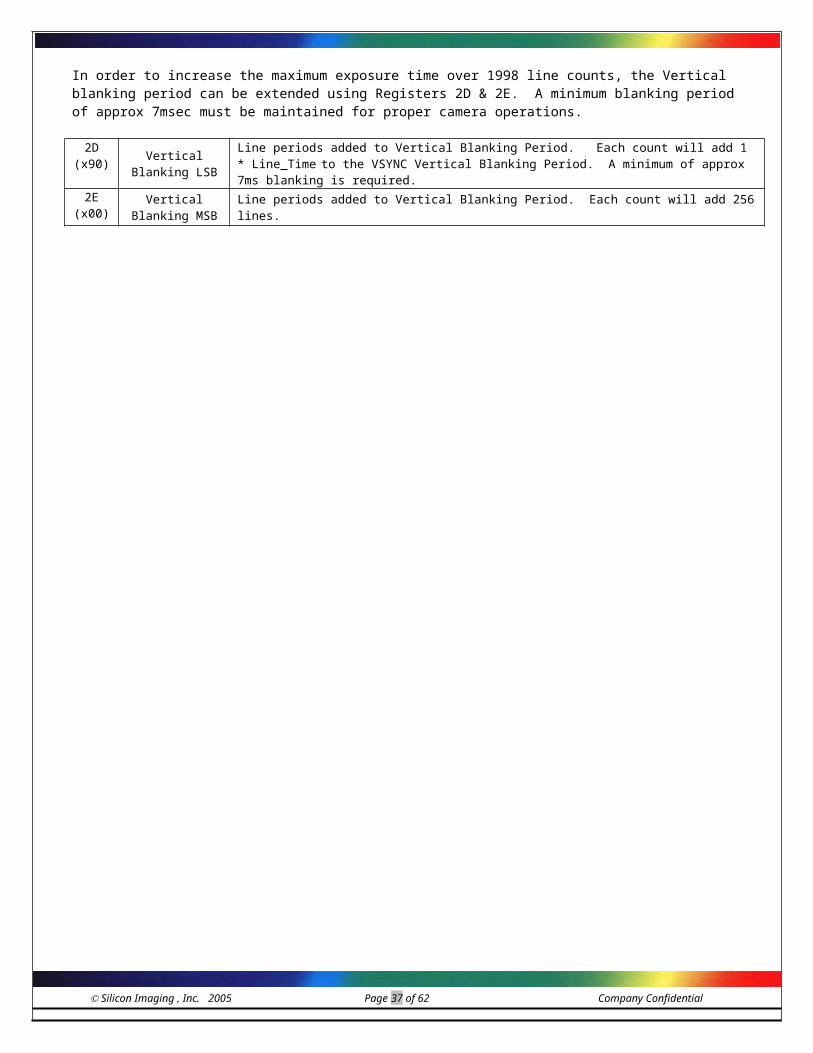
Long Exposure (Extended Vertical Blanking (VB))In order to increase the maximum exposure time over 1998 line counts, the Vertical blanking period can be extended using Registers 2D & 2E. A minimum blanking period of approx 7msec must be maintained for proper camera operations.
2D (x90) Vertical
Blanking LSBLine periods added to Vertical Blanking Period. Each count will add 1 * Line_Time to the VSYNC Vertical Blanking Period. A minimum of approx 7ms blanking is required.
2E (x00)
Vertical Blanking MSB Line periods added to Vertical Blanking Period. Each count will add 256 lines.
Silicon Imaging , Inc. 2005 Page 23 of 42 Company Confidential
Global Gain
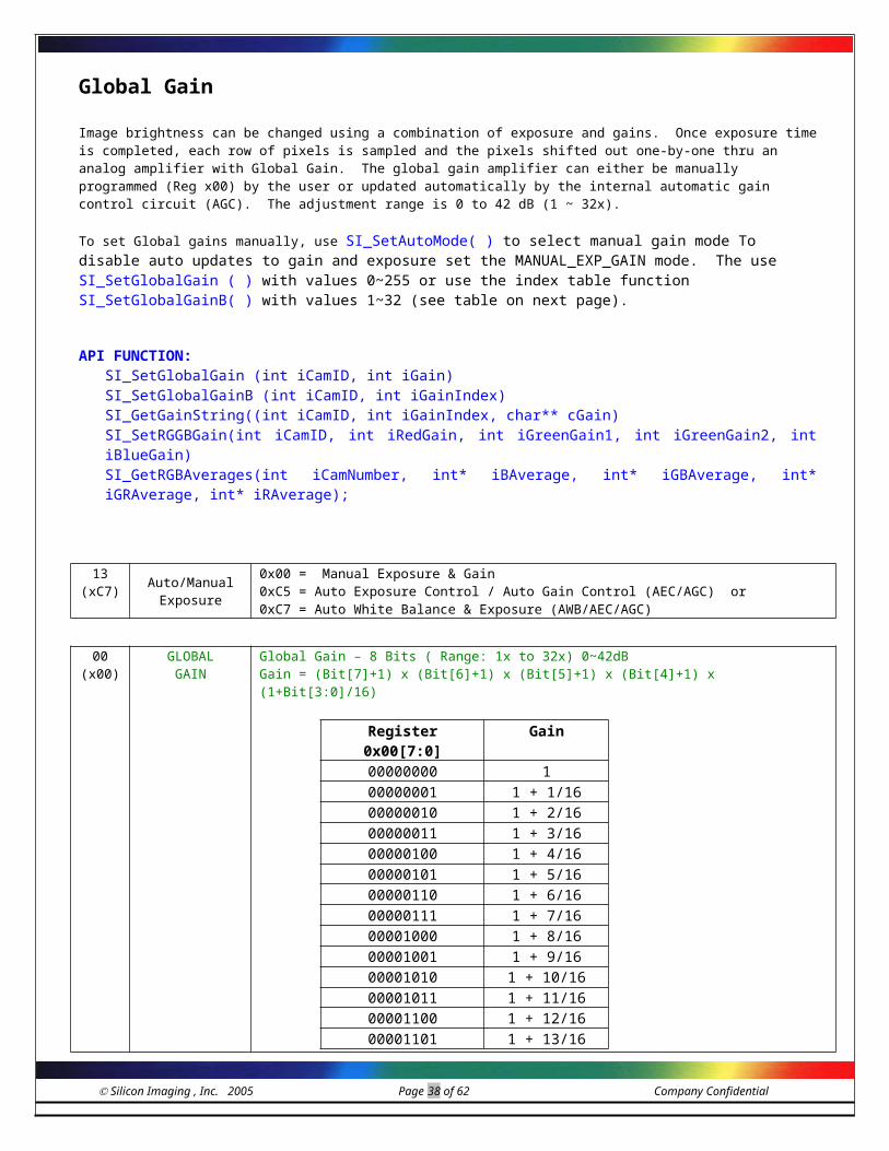
Image brightness can be changed using a combination of exposure and gains. Once exposure time is completed, each row of pixels is sampled and the pixels shifted out one-by-one thru an analog amplifier with Global Gain. The global gain amplifier can either be manually programmed (Reg x00) by the user or updated automatically by the internal automatic gain control circuit (AGC). The adjustment range is 0 to 42 dB (1 ~ 32x).
To set Global gains manually, use SI_SetAutoMode( ) to select manual gain mode To disable auto updates to gain and exposure set the MANUAL_EXP_GAIN mode. The use SI_SetGlobalGain ( ) with values 0~255 or use the index table function SI_SetGlobalGainB( ) with values 1~32 (see table on next page).
API FUNCTION:SI_SetGlobalGain (int iCamID, int iGain)SI_SetGlobalGainB (int iCamID, int iGainIndex)SI_GetGainString((int iCamID, int iGainIndex, char** cGain)SI_SetRGGBGain(int iCamID, int iRedGain, int iGreenGain1, int iGreenGain2, int iBlueGain)SI_GetRGBAverages(int iCamNumber, int* iBAverage, int* iGBAverage, int* iGRAverage, int* iRAverage);
13 (xC7) Auto/Manual
Exposure
0x00 = Manual Exposure & Gain0xC5 = Auto Exposure Control / Auto Gain Control (AEC/AGC) or0xC7 = Auto White Balance & Exposure (AWB/AEC/AGC)
00(x00)
GLOBAL GAIN
Global Gain – 8 Bits ( Range: 1x to 32x) 0~42dBGain = (Bit[7]+1) x (Bit[6]+1) x (Bit[5]+1) x (Bit[4]+1) x (1+Bit[3:0]/16)
Register 0x00[7:0] Gain00000000 100000001 1 + 1/1600000010 1 + 2/1600000011 1 + 3/1600000100 1 + 4/1600000101 1 + 5/1600000110 1 + 6/1600000111 1 + 7/1600001000 1 + 8/1600001001 1 + 9/1600001010 1 + 10/1600001011 1 + 11/1600001100 1 + 12/1600001101 1 + 13/1600001110 1 + 14/1600001111 1 + 15/1600010000 2 x (1 + 0/16)00110000 4 x (1 + 0/16)01110000 8 x (1 + 0/16)11110000 16 x (1 + 0 /16)11111111 16 x (1 +15/16)
Note: Set REG13[0,2} = 0 to disable AGC & AEC.14
(x40) AGC Max Bit[7:6]: Max AGC: 00 (2x), 01 (4x), 10 (8x), 11 (16x)Bit[5:0]: Reserved 00
Silicon Imaging , Inc. 2005 Page 24 of 42 Company Confidential
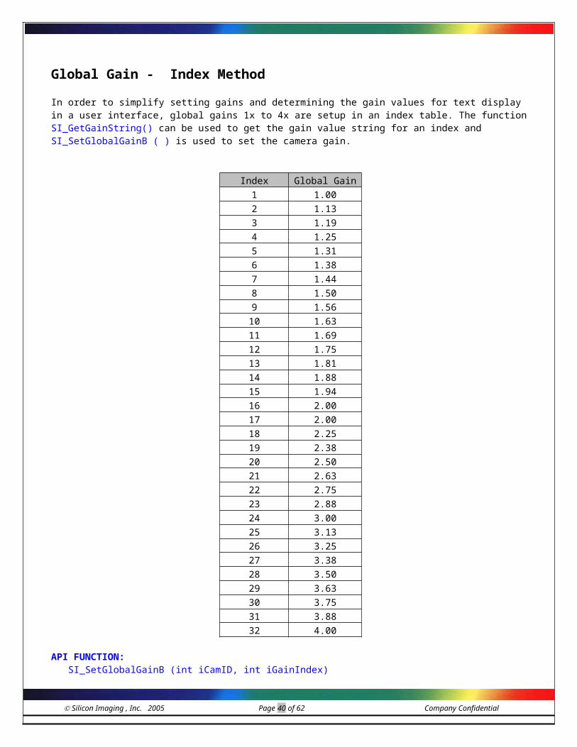
Global Gain - Index MethodIn order to simplify setting gains and determining the gain values for text display in a user interface, global gains 1x to 4x are setup in an index table. The function SI_GetGainString() can be used to get the gain value string for an index and SI_SetGlobalGainB ( ) is used to set the camera gain.
Index Global Gain1 1.002 1.133 1.194 1.255 1.316 1.387 1.448 1.509 1.5610 1.6311 1.6912 1.7513 1.8114 1.8815 1.9416 2.0017 2.0018 2.2519 2.3820 2.5021 2.6322 2.7523 2.8824 3.0025 3.1326 3.2527 3.3828 3.5029 3.6330 3.7531 3.8832 4.00
API FUNCTION:SI_SetGlobalGainB (int iCamID, int iGainIndex)SI_GetGainString((int iCamID, int iGainIndex, char** cGain)
Silicon Imaging , Inc. 2005 Page 25 of 42 Company Confidential
Auto White Balance (AWB)The SI-5100 continuously collects image statistics of the average output level data for the R/Gr/Gb/B channels and places them into registers (x05, x06, x07, x08) for calculated image white balance. The values are calculated from 128 pixels per line. The average of these 4 values is also calculated and placed in a Luminance Average register (Reg 2F) to be used for AEC/AGC control.
Use SI_SetAutoMode() to set the mode to AUTO_WHITE_BALANCE_EXP. This mode is also considered the fully automatic mode where the camera performs both AGC/AEC to get to the correct brightness levels and then does Auto White Balance gain adjustments of the Blue/Red Gains (Reg 01 & 02) to get matching R,G,B averages.
The AWB circuit will automatically update the Red & Blue gain values until they are within the threshold range (Reg3[7:4]) specified by SI_SetAWBThreshold( ). The speed of updates (Reg x04[7:4) is also set by the SI_SetAWBThreshold( ) function. The stability of the White Balance will vary on the lighting conditions and the tolerance of the AWB threshold.
API FUNCTION:SI_SetAutoMode(int iCamID, int iMode)SI_SetAWBThreshold(int iCamID, int iWhiteBalanceThresh, int iWhtetBalanceSpeed)SI_GetRGBAverages(int iCamNumber, int* iBAverage, int* iGBAverage, int* iGRAverage, int* iRAverage);
13 (xC7)
Auto/ManualExposure 0xC7 = Auto White Balance & Exposure (AWB/AEC/AGC)
03(x4A)
Auto White Balance
Threshold&
Vertical window (2LSB)
Bit[7:4]: AWB update threshold (0~15)
Bit[3:2]: Vertical window end line control 2 LSBsBit[1:0]: Vertical window start line control 2 LSBs
04 (x00)
Auto White BalanceSpeed
&
Exposure (3LSB)
Bit[7:6]: AWB Step Selection00: 1023 steps 10: 511 steps01: 255 steps 11: 255 steps
Bit[5:4]: AWB Update Speed Selection00: Slow 10: Fast01: Slowest 11: Fast
Bit[3]: ReservedBit[2:0]: Exposure lower 3 bits – AEC[2:0]
05 (x00)
BLUEAverage
B Channel Average BAVG[7:0] – Calculated from all Blue pixels in the image
06 (x00) GREEN (b)
AverageGb Channel Average GbAVG[7:0]- Picked G pixels in the same line with B pixels.
07 (x00) GREEN (r)
AverageGr Channel Average GrAVG[7:0] - Picked G pixels in the same line with R pixels.
08 (x00) RED
AverageR Channel Average RAVG[7:0] – Calculated from all Red pixels in the image
2F (x00) Average
Luminance Luminance Average = Calculated from the B/Gb/Gr/R channel average:AVG = (BAVG[7:0] + GbAVG[7:0] + GrAVG[7:0] +RAVG[7:0])/4)
Silicon Imaging , Inc. 2005 Page 26 of 42 Company Confidential
Manual Red/Blue White Balance Gain ControlThe Global Gain amplified signals are color balanced by adjusting the Blue and Red gains to match the Green. The Red Gain (Reg x02) and Blue gain (Reg x01) can be set manually by the user SI_SetRGGBGain( ) or by the internal automatic white balance (AWB) controller by setting SI_SetAutoMode() into AWB mode.
In AWB (Auto White Balance) mode, the Red/Blue channel gains are automatically increased or decreased to match Green channel luminance level (Reg 06, 07). The adjustment range is +/-9.5 dB (1/3 ~ 3x). The AWB can be used in combination with the AEC and AGC functions.
API FUNCTION:SI_SetAutoMode(int iCamID, int iMode)SI_SetRGGBGain(int iCamID, int iRedGain, int iGreenGain1, int iGreenGain2, int iBlueGain)SI_SetRGGBGainB(int iCamID, int iRedGainIndex, int iGreenGain1Index, int iGreenGain2Index, int iBlueGainIndex)
01(x80)
BLUE GAIN
[8 MSB]
Blue Gain Control - Range: 1/3x to 3x
If BLUE[7] = 1, then Blue gain = 1 + BLUE[6:0]/64If BLUE[7] = 0, then Blue gain = 1/(1 + BLUE_B[6:0]/64),
where BLUE_B[6:0] is the bit reverse of BLUE[6:0]. 0~127 = 1/(1+(128-REG)/64) 128-255 = 1+(REG-128)/64
02(x80)
RED GAIN
[8 MSB]
Red Gain Control - Range: 1/3x to 3x
If RED[9] = 1, then Red gain = 1 + RED[6:0]/64If RED[9] = 0, then Red gain = 1/(1 + RED_B[6:0]/64),
where RED_B[6:0] is the bit reverse of RED[6:0]. 0~127 = 1/(1+(128-REG)/64)
128-255 = 1+(REG-128)/64
Silicon Imaging , Inc. 2005 Page 27 of 42 Company Confidential
RED/BLUE GAIN TABLES
Register Gain Register Gain Register Gain0 0.33 51 0.45 102 0.711 0.34 52 0.46 103 0.722 0.34 53 0.46 104 0.733 0.34 54 0.46 105 0.744 0.34 55 0.47 106 0.745 0.34 56 0.47 107 0.756 0.34 57 0.47 108 0.767 0.35 58 0.48 109 0.778 0.35 59 0.48 110 0.789 0.35 60 0.48 111 0.7910 0.35 61 0.49 112 0.8011 0.35 62 0.49 113 0.8112 0.36 63 0.50 114 0.8213 0.36 64 0.50 115 0.8314 0.36 65 0.50 116 0.8415 0.36 66 0.51 117 0.8516 0.36 67 0.51 118 0.8617 0.37 68 0.52 119 0.8818 0.37 69 0.52 120 0.8919 0.37 70 0.52 121 0.9020 0.37 71 0.53 122 0.9121 0.37 72 0.53 123 0.9322 0.38 73 0.54 124 0.9423 0.38 74 0.54 125 0.9624 0.38 75 0.55 126 0.9725 0.38 76 0.55 127 0.9826 0.39 77 0.56 128 1.0027 0.39 78 0.56 129 1.0228 0.39 79 0.57 130 1.0329 0.39 80 0.57 131 1.0530 0.40 81 0.58 132 1.0631 0.40 82 0.58 133 1.0832 0.40 83 0.59 134 1.0933 0.40 84 0.59 135 1.1134 0.41 85 0.60 136 1.1335 0.41 86 0.60 137 1.1436 0.41 87 0.61 138 1.1637 0.41 88 0.62 139 1.1738 0.42 89 0.62 140 1.1939 0.42 90 0.63 141 1.2040 0.42 91 0.63 142 1.2241 0.42 92 0.64 143 1.2342 0.43 93 0.65 144 1.2543 0.43 94 0.65 145 1.2744 0.43 95 0.66 146 1.2845 0.44 96 0.67 147 1.3046 0.44 97 0.67 148 1.3147 0.44 98 0.68 149 1.3348 0.44 99 0.69 150 1.3449 0.45 100 0.70 151 1.3650 0.45 101 0.70 152 1.38
RED/BLUE GAIN TABLES (continued)Register Gain Register Gain
153 1.39 205 2.20154 1.41 206 2.22155 1.42 207 2.23156 1.44 208 2.25157 1.45 209 2.27158 1.47 210 2.28159 1.48 211 2.30
Silicon Imaging , Inc. 2005 Page 28 of 42 Company Confidential

160 1.50 212 2.31161 1.52 213 2.33162 1.53 214 2.34163 1.55 215 2.36164 1.56 216 2.38165 1.58 217 2.39166 1.59 218 2.41167 1.61 219 2.42168 1.63 220 2.44169 1.64 221 2.45170 1.66 222 2.47171 1.67 223 2.48172 1.69 224 2.50173 1.70 225 2.52174 1.72 226 2.53175 1.73 227 2.55176 1.75 228 2.56177 1.77 229 2.58178 1.78 230 2.59179 1.80 231 2.61180 1.81 232 2.63181 1.83 233 2.64182 1.84 234 2.66183 1.86 235 2.67184 1.88 236 2.69185 1.89 237 2.70186 1.91 238 2.72187 1.92 239 2.73188 1.94 240 2.75189 1.95 241 2.77190 1.97 242 2.78191 1.98 243 2.80192 2.00 244 2.81193 2.02 245 2.83194 2.03 246 2.84195 2.05 247 2.86196 2.06 248 2.88197 2.08 249 2.89198 2.09 250 2.91199 2.11 251 2.92200 2.13 252 2.94201 2.14 253 2.95202 2.16 254 2.97203 2.17 255 2.98204 2.19
Silicon Imaging , Inc. 2005 Page 29 of 42 Company Confidential
SI-5100 REGISTER TABLE
00(x00)
GLOBAL GAIN
Global Gain – 8 Bits ( Range: 1x to 32x) 0~42dBGain = (Bit[7]+1) x (Bit[6]+1) x (Bit[5]+1) x (Bit[4]+1) x (1+Bit[3:0]/16) Note: Set REG13[0,2} = 0 to disable AGC & AEC.
01(x80)
BLUE GAIN
[8 MSB]
Blue Gain Control - Range: 1/3x to 3x
If BLUE[7] = 1, then Blue gain = 1 + BLUE[6:0]/64If BLUE[7] = 0, then Blue gain = 1/(1 + BLUE_B[6:0]/64),
where BLUE_B[6:0] is the bit reverse of BLUE[6:0].
02(x80)
RED GAIN
[8 MSB]
Red Gain Control - Range: 1/3x to 3x
If RED[9] = 1, then Red gain = 1 + RED[6:0]/64If RED[9] = 0, then Red gain = 1/(1 + RED_B[6:0]/64),
where RED_B[6:0] is the bit reverse of RED[6:0].
03(x4A)
Auto White Balance
Threshold&
Vertical window (2LSB)
Bit[7:4]: AWB update threshold (0~15)
Bit[3:2]: Vertical window end line control 2 LSBsBit[1:0]: Vertical window start line control 2 LSBs
04 (x00)
Auto White BalanceSpeed
&
Exposure (3LSB)
Bit[7:6]: AWB Step Selection00: 1023 steps 10: 511 steps01: 255 steps 11: 255 steps
Bit[5:4]: AWB Update Speed Selection00: Slow 10: Fast01: Slowest 11: Fast
Bit[3]: ReservedBit[2:0]: Exposure lower 3 bits – AEC[2:0]
05 (x00) BLUE
AverageB Channel Average BAVG[7:0] – Calculated from all Blue pixels in the image
06 (x00) GREEN (b)
AverageGb Channel Average GbAVG[7:0]- Picked G pixels in the same line with B pixels.
07 (x00) GREEN (r)
AverageGr Channel Average GrAVG[7:0] - Picked G pixels in the same line with R pixels.
08 (x00) RED
AverageR Channel Average RAVG[7:0] – Calculated from all Red pixels in the image
10 (x43) AEC[10:3]
Exposure[8 CSB]
Exposure Time = t LINE x AEC[16:0] AEC[16:11] = Reg45[5:0] = 6MSB (these bits are not current set by SetExposureValue() AEC[10:3 ] = Reg10[7:0] = 8CSB AEC [ 2:0 ] = Reg04[2:0] = 3LSB***Note: Max Exposure time is 1 Frame period even if AEC is set longer than frame perod.
12 (x00) RES MODE
Bit[6:4]: Resolution Mode selection 2592 x 1944 QSXGA (000) 1280 x 960 SXGA (100) 640 x 480 VGA (010) 320 x 200 HF (001)
13 (xC7)
Auto/ManualExpsoure &
Bit[7]: AEC speed selection 0: Normal 1: Faster AEC correction
Silicon Imaging , Inc. 2005 Page 30 of 42 Company Confidential
White BalanceModes
0xC0 = Manual0xC5 = AEC0xC7 = AWB/AEC
Bit[6]: AEC speed/step selection 0: Small steps, slow 1: Big steps, fastBit[5:3]: 0Bit[2]: Exposure control 0: Manual 1: AutoBit[1]: AWB auto/manual control selection 0: Manual 1: AutoBit[0]: AGC auto/manual control selection 0: Manual 1: Auto
14 (xc2) AGC Max Bit[7:6]: Max AGC: 00 (2x), 01 (4x), 10 (8x), 11 (16x)
Bit[5:0]: Reserved 0216
(x00) ZOOM 0x00 = Zoom Off0x08 = Zoom On (Use in SXGA, VGA and HF Modes set in Reg 12)
17(x10)
HREFST(x14 in SXGA,
VGA, HF)
Horizontal Window Start most significant 8 bits, 3 least significant bits in HREF_LSB[2:0]HS[10:0]: Select beginning of horizontal window, each LSB represents two pixels
18 (xb2)
HREFEND(x64 in SXGA,
VGA, HF)
Horizontal Window End most significant 8 bits, 3 least significant bits in HREF_LSB[5:3] (x16)HE[10:0]: Select end of horizontal window, each LSB represents two pixels
19 (x00)
VSTRT Vertical Window line start most significant 8 bits, 2 LSBs in register COMA [1:0]VS[9:0]: Selects the start of the vertical window, each LSB represents two scan lines.
1A (xf3)
VEND1x78(SXGA)x3C (VGA)x19 (HV)
Vertical Window line end most significant 8 bits, 2 LSBs in register COMA [3:2]VE[9:0]: Selects the end of the vertical window, each LSB represents two scan lines.
24 (xA0)
Target Luminance
Max AEC
Luminance Signal High range for AEC/AGC operationAEC/AGC value is decrease in auto modes when average luminance is greater than AEH [7:0]
25 (x88)
Target Luminance
Min
Luminance Signal Low range for AEC/AGC operationAEC/AGC values will increase in auto mode when average luminance is less than AEL [7:0]
26(x52) AGC/AEC
Step Thresholds
Fast AEC/AGC Mode Large Step Range Threshold – BIT[7:4] = High threshold BIT[3:0] = Low ThresholdWhen luminance average is outside this range, large steps are applied. Within the range small step changes of gain/exposure occur until the average is within the target range.
2F (x00)
Average Luminance
Luminance AverageCalculated from the B/Gb/Gr/R channel average as follows:AVG = (BAVG[7:0] + GbAVG[7:0] + GrAVG[7:0] +RAVG[7:0])/4)
2D (x90)
Vertical Blanking
LSB
Line periods added to Vertical Blanking Period. Each count will add 1 * Line_Time to the VSYNC Vertical Blanking Period. A minimum of approx 7ms blanking is required.
2E (x00)
Vertical Blanking
MSBLine periods added to Vertical Blanking Period. Each count will add 256 lines.
32 (x36) HREF_LSB
Bit[7:6]: 0 0 Bit[5:3]: Horizontal window end position 3 LSBs xb6 = VGABit[2:0]: Horizontal window start position3 LSBs
39(x00) H_ZOOM
Bit[7:3]: 0Bit[2:0]: Horizontal window control in zoom mode (328 pixel increment)
45 (x00)
AEC_H[6 MSB]
Bit[7:6]: AGC[9:8} AGC highest gainBit[5:0]: AEC[16:11] Exposure value MSB
Silicon Imaging , Inc. 2005 Page 31 of 42 Company Confidential
4A
(x00)V_ZOOM1 Zoom Mode Vertical Window Start Point 8 MSBs
4B
(x00)V_ZOOM2
Zoom Mode Vertical Window Start Point Control 2 LSBBit[7:2]: ReservedBit[1:0]: Zoom mode vertical window start point LSB
Silicon Imaging , Inc. 2005 Page 32 of 42 Company Confidential
White Balance, Bayer Interpolation and Color Correction
White Balance and Color Correction are processing operations performed to ensure proper color fidelity in a captured digital camera image. In digital cameras an array of light detectors with color filters over them is used to detect and capture the image. This sensor does not detect light exactly as the human eye does, and so some processing or correction of the detected image is necessary to ensure that the final image realistically represents the colors of the original scene.
G R G RB G B GG R G RB G B G
Each pixel only represents a portion of the color spectrum and must be interpolated to obtain an RGB value per pixel. The Bayer color filter array (CFA) pattern, shown above, is a popular format for digital acquisition of color images [1]. Half of the total number of pixels are green (G), while a quarter of the total number is assigned to both red (R) and blue (B).
White Balance
The first step in processing the raw pixel data is to perform a white balance operation. A white object will have equal values of reflectivity for each primary color: ie:
R = G = B
An image of a white object can be captured and its histogram analyzed. The color channel that has the highest level is set as the target mean and the remaining two channels are increased with a gain multiplier to match. For example, if Green channel has the highest mean, gain ‘a’ is applied to Red and gain ‘b’ is applied to Blue.
G’ = R’a = bB’
The White Balance will vary, based on the color lighting source (Sunlight, Fluorescent, Tungsten) applied to the object and the amount of each color component within it. A full color natural scene can also be processed in the same fashion. This “Gray World” method assumes that the world is gray and the distribution of primaries color will be equal.
The “White Patch” method attempts to locate the objects that are truly white, within the scene; by assuming the whites pixels are also the brightest (I = R+G+B). Then, only the top percentage intensity pixels are included in the calculation of means, while excluding any pixels that may have any channel that is saturated.
Silicon Imaging , Inc. 2005 Page 33 of 42 Company Confidential

Bayer Interpolation
To convert an image from the bayer format to an RGB per pixel format, we need to interpolate the two missing color values in each pixel. Several standard interpolation methods (nearest neighbor, linear, cubic, cubic spline, etc.) were evaluated on this problem in [2]. The authors have measured interpolation accuracy as well as the speed of the method and concluded that the best performance is achieved by a correlation-adjusted version of the linear interpolation. The suggested method is presented here.
Interpolating red and blue components
G B GR G RG B G
(a)
G R GB G BG R G
(b)
B G BG R GB G B
(c)
R G RG B GR G R
(d)
Figure 1: Four possible cases for interpolating R and B components
As suggested in [2], R and B values are interpolated linearly from the nearest neighbors of the same color. There are four are possible cases, as shown in Figure 1. When interpolating the missing values of R and B on a green pixel, as in Figure 1 (a) and (b), we take the average values of the two nearest neighbors of the same color. For example, in Figure 1 (a), the value for the blue component on a shaded G pixel will be the average of the blue pixels above and below the G pixel, while the value for the red component will be the average of the two red pixels to the left and right of the G pixel.
Figure 1 (c) shows the case when the value of the blue component is to be interpolated for an R pixel. In such case, we take the average of the four nearest blue pixels cornering the R pixel. Similarly, to determine the value of the red component on a B pixel in Figure 2 (d) we take the average of the four nearest red pixels cornering the B pixel.
Interpolating the green component
By [2], green component is adaptively interpolated from a pair of nearest neighbors. To illustrate the procedure, consider two possible cases in Figure 2.
R1
G1
R4 G4 R G2 R2
G3
R3
(a)
B1
G1
B4 G4 B G2 B2
G3
B3
(b)
Figure 2: Two possible cases for interpolating G component
In Figure 2 (a), the value of the green component is to be interpolated on an R pixel. The value used for the G component here is
Silicon Imaging , Inc. 2005 Page 34 of 42 Company Confidential
In other words, we take into account the correlation in the red component to adapt the interpolation method. If the difference between R1 and R3 is smaller than the difference between R2 and R4, indicating that the correlation is stronger in the vertical direction, we use the average of the vertical neighbors G1 and G3 to interpolate the required value. If the horizontal correlation is larger, we use horizontal neighbors. If neither direction dominates the correlation, we use all four neighbors.
Similarly, for Figure 2 (b) we will have
To conclude this section, note that if the speed of execution is the issue, one can safely use simple linear interpolation of the green component from the four nearest neighbors, without any adaptation
According to [2], this method of interpolation executes twice as fast as the adaptive method, and achieves only slightly worse performance on real images. For even fast updates only two of the four green values are averaged. However, this method displays false color on edges or zipper artifacts.
Color Saturation MatrixThe operation for saturation can be applied at the same time as the color correction matrix. Unlike the color correction matrix, the saturation matrix does not rotate the vectors in the color wheel:
[m00 m01 m02] [ R ] [m10 m11 m12] * [G ] [m20 m21 m22] [ B ]
m00 = 0.299 + 0.701*K m01 = 0.587 * (1-K) m02 = 0.114 * (1-K)
m10 = 0.299 * (1-K) m11 = 0.587 + 0.413*K m12 = 0.114 * (1-K)
m20 = 0.299 * (1-K) m21 = 0.587 * (1-K) m22 = 0.114 + 0.886*K
K is the saturation factor K=1 means no change K > 1 increases saturation 0<K<1 decreases saturation, K=0 produces B&W , K<0 inverts color
A sample table of matrix values are calculated and shown below:
Saturation Saturation Saturation Saturation
1 1.7 1.9 2R’ = +R* 1.0 1.4907 1.6309 1.701
+G* 0 -0.4109 -0.5283 -0.587+B* 0 -0.0798 -0.1026 -0.114
G’ = +R* 0 -0.2093 -0.2691 -0.299+G* 1.0 1.2891 1.3717 1.413+B* 0 -0.0798 -0.1026 -0.114
B’ = +R* 0 -0.2093 -0.2691 -0.299+G* 0 -0.4109 -0.5283 -0.587+B* 1.0 1.6202 1.7974 1.886
Silicon Imaging , Inc. 2005 Page 35 of 42 Company Confidential
Monochrome Saturation Matrix
A monochrome image can now be easily obtained from a color image by setting K=0
m00 = 0.299 m01 = 0.587 m02 = 0.114
m10 = 0.299 m11 = 0.587 m12 = 0.114
m20 = 0.299 m21 = 0.587 m22 = 0.114
Color Correction Matrix
The saturated image can be further processed with an additional color correction matrix to compensate for cross-talk induced by the micro-lens and color filter process, lighting and temperature effects. The combination matrix ([color correction matrix] * [saturation matrix]) results in a closer to true world color representation, but an increase in noise. Typically, the blue pixel has the lowest pixel response and the highest Crosstalk from the Green and Red light. The resulting noise after matrix operation is a high degree of blue noise.
A sample color matrix for the SI-5100 color matrix settings are in Table below:
R G BR’ = 1.268 <0.094> <0.051>G’ = <0.872> 1.821 <0.051>B’ = <0.101> *<0.126> 1.227
Conversion between RGB and YUV
We give two commonly used forms of equations for conversion between RGB and YUV formats. The first one is recommended by CCIR [3]
(2.1)
The second form is used by Intel in their image processing library [4], and may be more suitable for implementation:
(2.2)
In either case, resulting values of Y, U and V should be clipped to fit the appropriate range for the YUV format (e.g. [0,255] for a 24-bit YUV format). The inverse conversion may be accomplished by:
(2.3)
References
[1] B. E. Bayer, Color imaging array, US Patent No. 3971065.[2] T. Sakamoto, C. Nakanishi and T. Hase, “Software pixel interpolation for digital still cameras suitable for a 32-
bit MCU,” IEEE Trans. Consumer Electronics, vol. 44, no. 4, November 1998.{3} http://www.northpoleengineering.com/rgb2yuv.htm
Silicon Imaging , Inc. 2005 Page 36 of 42 Company Confidential
SI-5100 Spectral Response Curve
SI-5100-RGB Cover Glass Filter Response (IRC-30)
Silicon Imaging , Inc. 2005 Page 37 of 42 Company Confidential
Binary to Hex (ASCII) TableBinary Hex in ASCII0000 00001 10010 20011 30100 40101 50110 60111 71000 81001 91010 a1011 b1100 c1101 d1110 e1111 f
FRONT VIEW
Silicon Imaging , Inc. 2005 Page 38 of 42 Company Confidential

SI-5100 USB ENCLOSURE DIMENSIONS
Silicon Imaging , Inc. 2005 Page 39 of 42 Company Confidential
SI-5100 PCB DIMENSIONS
Silicon Imaging , Inc. 2005 Page 40 of 42 Company Confidential
SI-5100RGB SAMPLE COLOR IMAGE
Silicon Imaging , Inc. 2005 Page 41 of 42 Company Confidential

Contact Information
Silicon Imaging, Inc.www.siliconimaging.com
Ordering InformationSI-5100RGB-U 5.1 Megapixel RGB Bayer Color USB2.0 MegaCamera
Legal DisclaimerSilicon Imaging reserves the right to make changes to its products or to discontinue any product or service without notice, and advises customers to obtain the latest version of relevant information to verify, before placing orders, that information being relied on is current and complete. No license, express or implied to any intellectual property rights is granted by this document.
Specific testing of all parameters of each device is not necessarily performed, except those mandated by government requirements.
CERTAIN APPLICATIONS USING SEMICONDUCTOR PRODUCTS MAY INVOLVE POTENTIAL RISKS OF DEATH, PERSONAL INJURY, OR SEVERE PROPERTY OR ENVIRONMENTAL DAMAGE ("CRITICAL APPLICATIONS"). SILICON IMAGING PRODUCTS ARE NOT DESIGNED, AUTHORIZED, OR WARRANTED TO BE SUITABLE FOR USE IN LIFE-SUPPORT DEVICES OR SYSTEMS OR OTHER CRITICAL APPLICATIONS. INCLUSION OF SILICON IMAGING PRODUCTS IN SUCH APPLICATIONS IS UNDERSTOOD TO BE FULLY AT THE CUSTOMER'S RISK.
The Product described in this datasheet may contain design defects or errors known as errata which may cause the product to deviate from published specifications. Current characterized errata are available upon request.
Copyright: Silicon Imaging, Inc., 2005
Silicon Imaging , Inc. 2005 Page 42 of 42 Company Confidential