managing the evolution of flash : beyond memory to … the evolution of flash: beyond memory to...
TRANSCRIPT
Managing the evolution of Flash: beyond memory to storage
Tony Kim
Director, Memory MarketingSamsung Semiconductor I nc.
Nonvolatile Memory SeminarHot Chips Conference
August 22, 2010Memorial AuditoriumStanford University

Contents
NAND Flash technology Flash storage management Flash storage architecture by apps Future trend Conclusions

Contents
NAND Flash technology Flash storage management Flash storage architecture by apps Future trend Conclusions
3 / 34
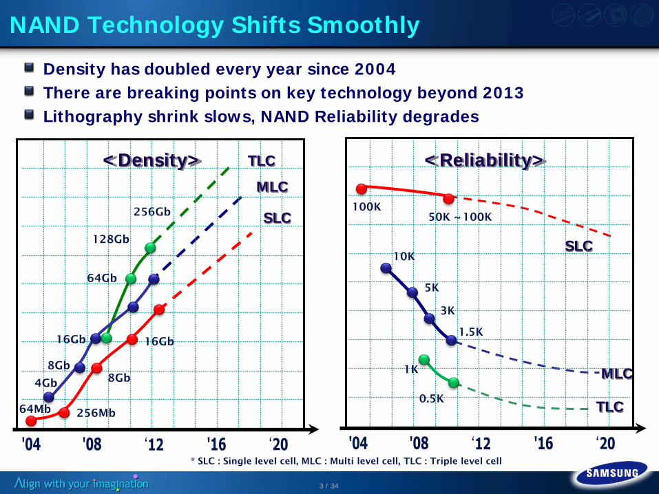
NAND Technology Shifts Smoothly
Density has doubled every year since 2004There are breaking points on key technology beyond 2013Lithography shrink slows, NAND Reliability degrades
MLC
SLC
TLC
10K
100K50K ~ 100K
1.5K
5K
< Reliability>
4Gb
8Gb
64Gb
16Gb
256Mb
128Gb
< Density>
64Mb
256Gb
16Gb
8Gb1K
0.5K
3K
TLC
MLC
SLC
* SLC : Single level cell, MLC : Multi level cell, TLC : Triple level cell
4 / 34
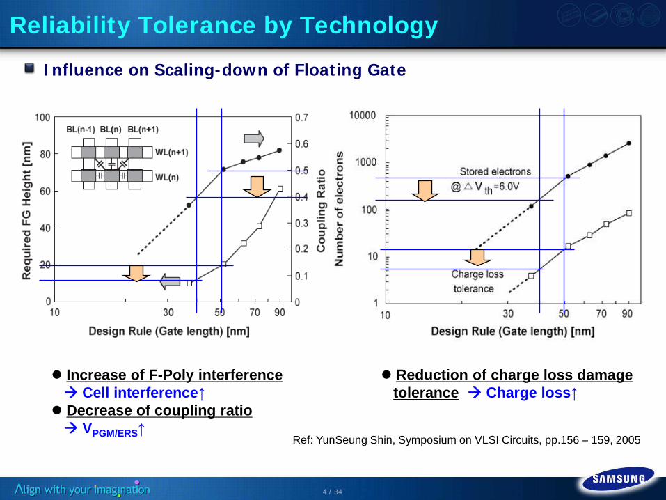
Reliability Tolerance by Technology
I nfluence on Scaling -down of Floating Gate
Increase of F -Poly interference Cell interference ↑
Decrease of coupling ratio VPGM/ERS↑
Reduction of charge loss damagetolerance Charge loss ↑
Ref: YunSeung Shin, Symposium on VLSI Circuits, pp.156 – 159, 2005

5 / 34
JEDEC Standard : Cycle & Data Retention
Density Write operations should occur across device life time10 year retention after lifetime write cycle is unp ractical
Endurance cycle
Data retention
Endurance cycle Data retention
Max. spec cycleMax. spec cycle 10years
Until 2006 As of 2007
100% END Cycle + 10y DTN10% END Cycle + 10y DTN
100% END Cycle + 1y DTN

6 / 34
Controller : Crit ical for Maintaining Reliability
More intelligence of controller can offset some of the generic degradation of NAND reliability from scaling
Technology
Target Endurance
1 K
3 K
4 xnm 3 xnm 2 xnm
Endurance
3bit
2bit
Role of Controller
Endurance of cell

7 / 34
NAND
EC
C E
ng
ine
FT
L(S
/W
)
Legacy Controller
VthR1 R2 R3 R4 R5 R6 R7
3 bit MLC
Bit errors
Technology Engine with ECC/ Bit Error/ FTL
Legacy controller only with ECC cannot reliably han dle 2 bit in 3xnm and beyond, let alone 3 bitOptimization with Flash cell characteristics in min d is crucialNew metric for reliability measurement is needed su ch as lifetime data amount w ith standard pattern
Ho
st
I/F
EC
C E
ng
ine
FT
L(S
/W
)
Ho
st
I/F
Bit
Err
or
En
gin
e
NAND
New ControllerMelded together

8 / 34
Samsung’s I nnovative Flash Technology
Samsung is exploring new technology to break status -quoSamsung believes 3D -NAND is the most likely successor for Planar NANDin the coming future
Planar NAND 3D-NAND
Cellarchitecture
AdvantagesEasy to produce with
simple processHigh reliabilityProcess reuse
ChallengesHard to shrink under
1xnmHard to stack

9 / 34
3D-NAND details
Potential benefit• Better reliability/ endurance than planar since cell design rule is
much more relaxed.
I ssues in future scaling• Bit cost reduction is done by increasing the stacki ng layer, thereby
increasing by 2X per each generation becomes more d ifficult and unlikely• Block size will be larger than the planar -equivalent
CSL
ControlGate(W/L)
GSLGate
SSLGate
n+
n+ p-Sub
n+
0
0.5
1
1.5
2
2.5
3
3.5
4
4.5
8 16 24 32
W/L share 8
W/L share 6
W/L share 4
Stacking layer #
Block Size (MB)

Contents
NAND Flash technology Flash storage management Flash storage architecture by apps Future trend Conclusions

11 / 34
Why Software I s Needed for Flash?
Small data unit in Program and the large unit in Er ase requires another block newly allocated through mapp ing
Logical block #1 is mapped to physical block #1 and #N after updating
Block #1
page
pagepagepagepage
….
Block #N
Block #1
New Data
Invalidated
Valid Data
Copy
Logical #1
#1 #1
Log.
Phy.
Map Table #1 #1
#N
Log. Phy.
Map Table (updated)
updatingNew Data
New Data

12 / 34
FTL (Flash Translation Layer)
Manages mapping from logical to physical addressDetects and maps out Bad BlocksDoes Wear - leveling for life extension
Managed NAND
File System
Application
FTL
File System
Application
FTL
NAND Flash
Host Driver
NAND
Sector Read/Write
Page Read/ Program/Erase
Sector Read/Write
13 / 34
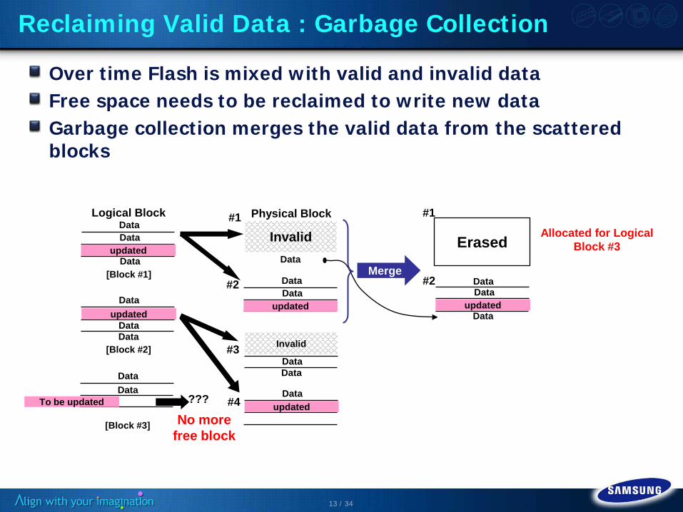
Reclaiming Valid Data : Garbage Collection
Over time Flash is mixed with valid and invalid dat aFree space needs to be reclaimed to write new dataGarbage collection merges the valid data from the s cattered blocks
DataData
updated
Data
updated
[Block #1]
[Block #2]
Data
[Block #3]
Data
DataData
updated
Data Data
Invalid
DataData
Dataupdated
Physical BlockLogical Block #1
#2
#3
#4???
No more free block
Merge
Erased
#1
Dataupdated
Data
Data
#2
Allocated for Logical Block #3
Invalid
To be updated
DataData

14 / 34
What is WAI (Wear Acceleration I ndex)?
WAI : The index that represent how much FTL acceler ate the wear -out of NAND
WriteSizeBlockSizeEraseCount
WAIBytes
BytesTotal×
=
FTL
Write Request (2 blocks)
Write (4 blocks) + Erase (4 blocks)
2256
1284=
×=
KB
KBWAI
* Block Size: 128KB
WAI NAND Life t ime Meaning
High Short Bad
Low Long Good
Example:
NAND

15 / 34
What is Wear - leveling ?
Hot data like FAT can wear out certain portion of c ell arrayWear- leveling maximizes the life span of NAND flash as e ach cell is used evenly
Before Wear-leveling After Good Wear -leveling
EraseCount
EraseCount
Block Num ber Block Num ber
Every cell is used evenly
FAT Data
Frequent Update

Contents
NAND Flash technology Flash storage management Flash storage architecture by apps Future trend Conclusions

17 / 34
NAND Flash Market Outlook ( ` 10 ~ ` 15)
Samsung expected NAND Market CAGR of 53% between 20 10 and 2015 Key applications for NAND market growth for next de cade are: Flash Card, Smart Phone, Tablet PC and SSD
W/W
Ann
ual U
nit
@1
6G
b E
quiv
. [B
illio
ns]
TabletPC
SSD
SmartPhone
2010-2015, 5-Yr CAGR: 53%
( Source : Samsung )Year
FlashCard6.7 Billion
56 Billion

18 / 34
Performance Multiplied with Multi -Chips
Flash storage performance can be easily expanded wi th multi -way write interleaving along with multi -channelsDuring program Busy, data can be loaded and program med into other NAND devices on the same bus
Flash Controller
nCE1
nCE2
nCE3
nCE4
NAND ControllerNo.1
NAND ControllerNo.2
I / O’s
I / O’s
Load PROGRAM
nCE1Load
Load LoadnCE2PROGRAM
CH 1
0
1000
2000
3000
4000
5000
1 2 4 8 16
Write I OPS
Number of chips
Flash Storage architecture

19 / 34
Application Segmented by Technology
Applications will be fragmented by performance and reliabilityCloser communications needed to understand user req uirements and tailor appropriate solutions
500
50
1K
3K
1.5K
30K
100K
300K
End
ura
nce
2.5MB/s 5MB/s 8MB/s 13MB/s
Write Performance
TLC
MLC
SLC
Consumer Card,UFD
SD Class2
Consumer Card,UFD
SD Class4,OEM UFD
SD Class4
MP3 , PND MP3 , PND
SD Class6
SD Class6
Consumer SSDMobile Phone,
PMP
Mid -End Enterprise SSD
Low -End Server SSD
High -End Card
High -End Server SSD
Tablet,
Contents
NAND Flash technology Flash storage management Flash storage architecture by apps Future trend Conclusions

21 / 34
Storage Architecture Evolution : Technical Trend
New environment on the storage drives higher perfor manceMulti tasking with Swap IO
High performance App with fast data IO
High bandwidth Network with User Data IO
2009 2010 2011 2012 2013
20
40
60
80
100
Former eMMC
eMMC 4.4
150
UFS
11~ 40Mbps 802.11b
1Gbps 802.11ac
54Mbps 802.11g
600Mbps 802.11n
300Mbps 802.11n~ g
1.3Gbps UWB
NetworkEnvironment
System Environment
DataEnvironment
- Single Task
-Multi Task-App install-Web access
-Multi Task-Full browsing-Multimedia play-Async I O & Sync I O
-Multimedia Data-App Data-Data base
-Swap Data-Web Cache-HD Media File-Small Random I O-Big Size Sequential Write
-Text Data-Photo Data
Storage Bandwidth [MB/ sec]
22 / 34
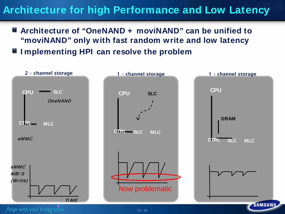
Architecture for high Performance and Low Latency
Architecture of “OneNAND + moviNAND” can be unified to “moviNAND” only with fast random write and low late ncyI mplementing HPI can resolve the problem
CTRL MLC
OneNAND
eMMC
SLCCPU SLC
MLCSLCCTRL
CPU CPU
MLCSLCCTRL
DRAM
eMMC
MB/ S
( W r i t e)
TI ME
2 – channel storage 1 – channel storage 1 – channel storage
Now problematic

23 / 34
Preparing Host for New Features of eMMC & UFS
The enhancements in read/ write performance, data in tegrity at sudden system -power failure and lower power consumption at idle are only realized with the relevant support of file -system, and OS in some casesLinux open source community is far behind in aligni ng to themChipset and handset vendors should work out the res ponsibility details
Features Purpose eMMC UFS
Trim Write speed up √ √
Reliable write Data integrity at power-loss √ √
HPI Write-suspend for fast read access √ √
Command queuing Read/Write speed up √
Sleep Power Lower power at idle √ √
24 / 34
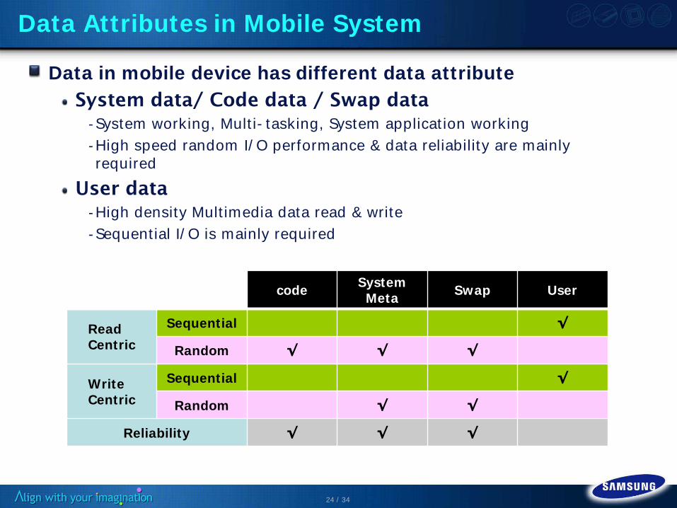
Data Attributes in Mobile System
Data in mobile device has different data attributeSystem data/ Code data / Swap data
- System working, Mult i- tasking, System applicat ion working- High speed random I/ O performance & data reliability are mainly required
User data- High density Mult imedia data read & write- Sequent ial I/ O is mainly required
codeSystem
MetaSwap User
Read Centric
Sequential √
Random √ √ √
Write Centric
Sequential √
Random √ √
Reliability √ √ √

25 / 34
New Feature for e -MMC 4.4 : Multi Partit ion
Flexibility to host to manage eMMC 4.44 general purpose partitions and enhanced user data area can be set in normal user data area
Partitions NAND type Default Size Remarks
Boot Area Partition 1 SLC Mode 128KB Size as multiple of 128KB (max. 32MB)
Boot Area Partition 2 SLC Mode 128KB Size as multiple of 128KB (max. 32MB)
RPMB Area Partition SLC Mode 128KB Size as multiple of 128KB (max. 32MB)
General Purpose PartitionsMLC “or” Enhanced Area
0KBAvailable size can be seen by following:(EXT_CSD[145]* 82 + EXT_CSD[144]* 81 + EXT_CSD[143]) *HC_WP_GPR_SIZE*HC_ERASE_GPR_SIZE * 512KB byte
User Data Area
Enhanced Area SLC Mode 0KB Start address multiple of Write Protect Group size
Default Area MLC 93.1%
Normal User Data Area
Boot 1 Boot 2 RPMB(Secure Data)
General Purpose Partition
Enhanced User data area(SLC mode)

26 / 34
Data Usage Model in eMMC4.4
SLC and MLC partit ions to be tailored by use scenar ios
Boot Area Partit ion
RPMB Area Partit ion
eMMC 4.4
General Purpose Area Partit ion 1
General Purpose Area Partit ion 2
User Data Area Partit ion
Enhanced User Data Area Partit ion
Host Side Data
Boot Code System Code
System File Security Data
Swap Data Application Code
User Data
SLC
MLC
Read I O, Reliability
Read I O, Reliability
Read/ Write I O, Sequential Pattern

27 / 34
Better Multi - tasking Performance with Trim
Trim reduces long write latency and in turn read la tency at multi - tasking. Mobile phones very likely having some free space benefit from Trim
No Impact as File Deleted
Performance Increase as Files Deleted
(Source : Microsoft)
Thread 1(4k RD)
Thread 2(64K WR)
ProgramMerge ProgramMerge
RD RD RD
Program Program Program Program
Thread 1(4k RD)
Thread 2(64K WR)
RD RD RDRD
Conceptual view of increased read thread due to long write thread with Busy

28 / 34
How Write Latency Affects for Multi - tasking
PROCESS A
PROCESS B
Tradit ional eMMC
HOST
Device
Download Data
MP3 PLAY
Write
Read
APP STOP
MB/ s
( W r it e)
TI ME
I nternal Write(Merge)
Multi - tasking needs low write latency in a time -out value for uninterrupted audio/ video play -back
29 / 34
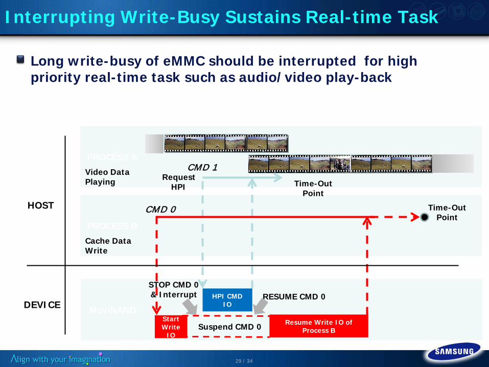
I nterrupting Write -Busy Sustains Real - t ime Task
Long write -busy of eMMC should be interrupted for high priority real - time task such as audio/ video play -back
PROCESS A
PROCESS B
MoviNANDStart Write
I O
HPI CMD I O
Resume Write I O of Process B
Request HPI Time -Out
Point
Time -Out Point
HOST
DEVI CE
Cache Data Write
Video Data Playing
Suspend CMD 0
STOP CMD 0 & I nterrupt
CMD 0
CMD 1
RESUME CMD 0

30 / 34
Next Generation Embedded Storage : UFS
Universal Flash Storage based on serial M -PhySerial interface : 300MB/s bandwidth
Native Command Queuing : Support parallel NAND Flash working for Random/Sequential IO
Page mapping with DRAM : Reduce internal Merge operation
CTRL
DRAM
NCQ w/ Q depth 4
CMD1
CMD2
CMD3
CMD4
HOST
300MB/ sSerial I nterface
System DataCode data Swap data User data
Page Mapping & Data Buffer with DRAM
31 / 34
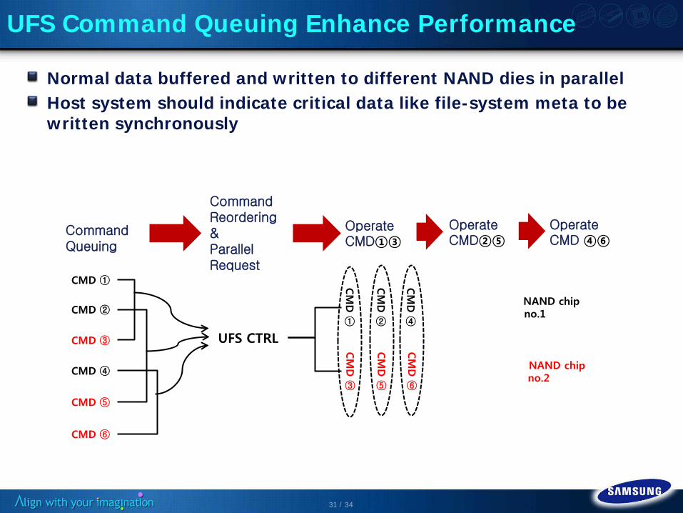
UFS Command Queuing Enhance Performance
Normal data buffered and written to different NAND dies in parallelHost system should indicate crit ical data like file -system meta to be written synchronously
CMD ①
CMD ③
CMD ②
CMD ④
CMD ⑤
CMD ⑥
UFS CTRL
NAND chip no.1
NAND chip no.2
Operate CMD①③
Operate CMD②⑤
Operate CMD ④⑥
CommandQueuing
Command Reordering&ParallelRequest
CM
D
①CM
D
③
CM
D
②
CM
D
④
CM
D
⑤
CM
D
⑥
32 / 34
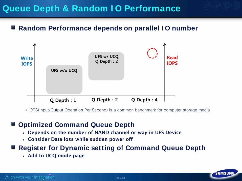
Queue Depth & Random I O Performance
* IOPS(Input/Output Operation Per Second) is a common benchmark for computer storage media
WriteIOPS
ReadIOPS
UFS w/o UCQ
UFS w/ UCQQ Depth : 2
Q Depth : 1 Q Depth : 2 Q Depth : 4
Random Performance depends on parallel I O number
Optimized Command Queue Depth Depends on the number of NAND channel or way in UFS Device
Consider Data loss while sudden power off
Register for Dynamic setting of Command Queue DepthAdd to UCQ mode page
33 / 34
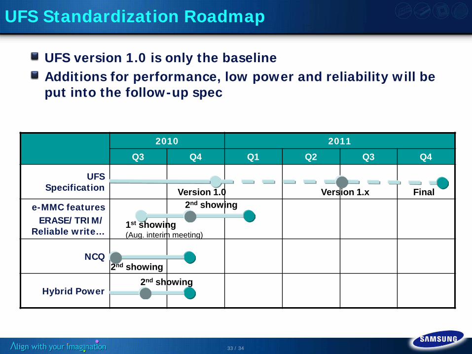
UFS Standardization Roadmap
UFS version 1.0 is only the baselineAdditions for performance, low power and reliabilit y w ill be put into the follow -up spec
2010 2011
Q3 Q4 Q1 Q2 Q3 Q4
UFS Specification
e-MMC featuresERASE/ TRI M/
Reliable write…
NCQ
Hybrid Power
Version 1.0 Version 1.x Final
1st showing(Aug. interim meeting)
2nd showing
2nd showing
2nd showing
34 / 34
Conclusions
Various NAND Flash technology target different mark ets with different focus in architecture and performanc e, resulting in w ider product portfolio
High performance mobile systems should tailor the u se of different NAND Flash technology of single storage w ith regards to performance and reliability for various application scenarios
NAND-friendly system -level solutions such as Trim, HPI as well as Reliable Write on eMMC will play a crit ical role in managing high reliability and performance
Command queue architecture on UFS provides a path t o future high performance by significantly increasing effective I OPS