mambo iii user manual version: 1 - particle...
TRANSCRIPT

1
MAMBO III User Manual
Version: 1.0
Farah Khalid
Alpana Shenai
Gregory Deptuch
Microelectronics ASIC Design
2
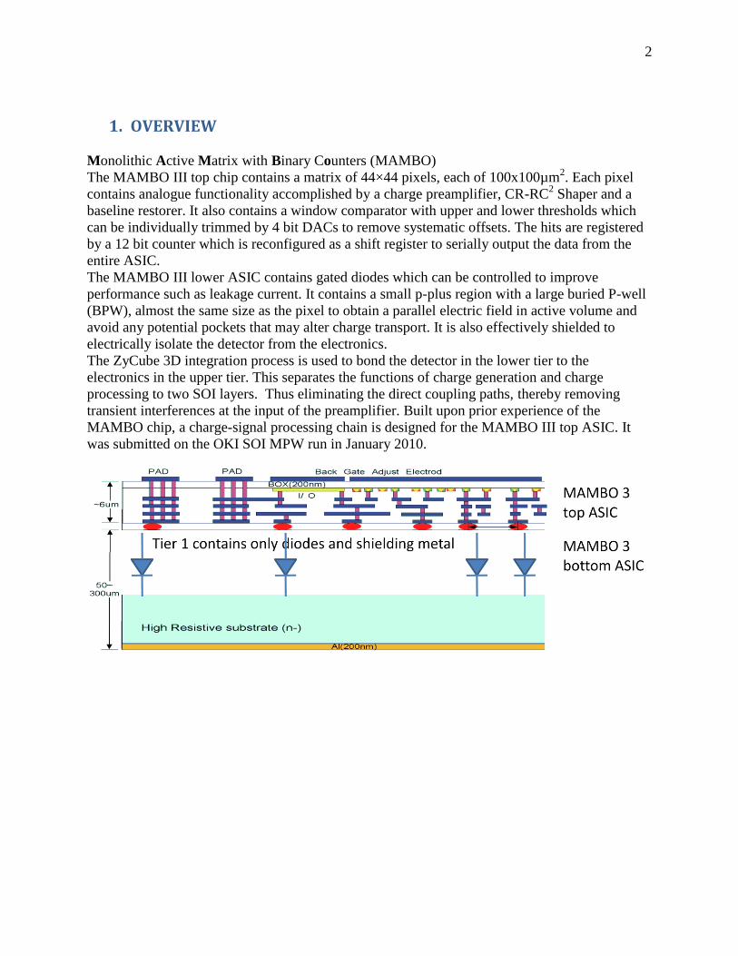
1. OVERVIEW
Monolithic Active Matrix with Binary Counters (MAMBO)
The MAMBO III top chip contains a matrix of 44×44 pixels, each of 100x100µm2. Each pixel
contains analogue functionality accomplished by a charge preamplifier, CR-RC2 Shaper and a
baseline restorer. It also contains a window comparator with upper and lower thresholds which
can be individually trimmed by 4 bit DACs to remove systematic offsets. The hits are registered
by a 12 bit counter which is reconfigured as a shift register to serially output the data from the
entire ASIC.
The MAMBO III lower ASIC contains gated diodes which can be controlled to improve
performance such as leakage current. It contains a small p-plus region with a large buried P-well
(BPW), almost the same size as the pixel to obtain a parallel electric field in active volume and
avoid any potential pockets that may alter charge transport. It is also effectively shielded to
electrically isolate the detector from the electronics.
The ZyCube 3D integration process is used to bond the detector in the lower tier to the
electronics in the upper tier. This separates the functions of charge generation and charge
processing to two SOI layers. Thus eliminating the direct coupling paths, thereby removing
transient interferences at the input of the preamplifier. Built upon prior experience of the
MAMBO chip, a charge-signal processing chain is designed for the MAMBO III top ASIC. It
was submitted on the OKI SOI MPW run in January 2010.
3
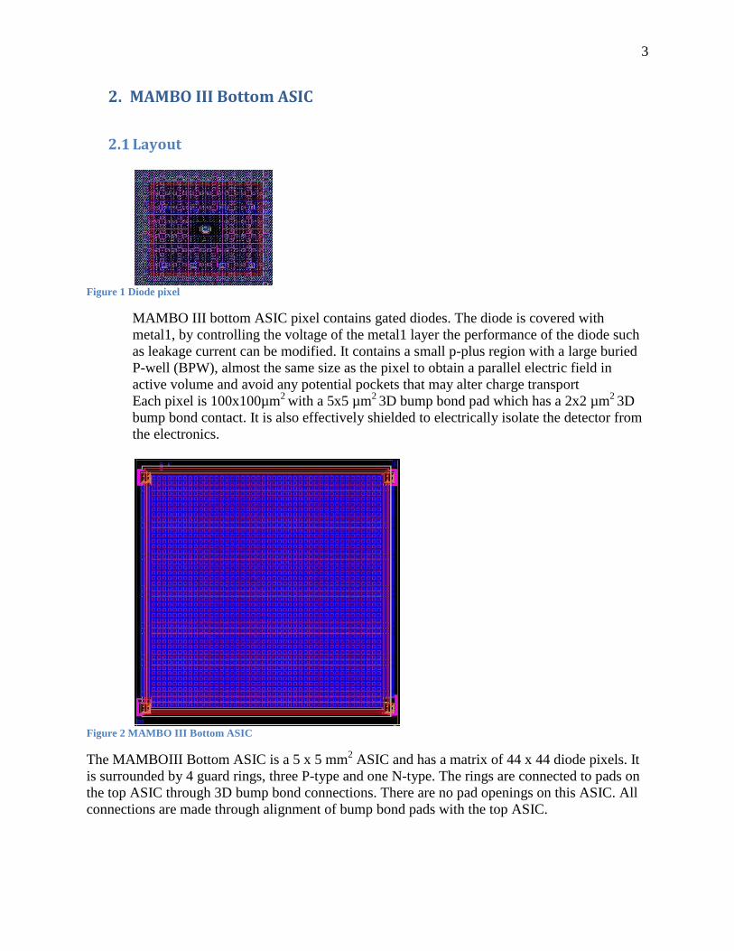
2. MAMBO III Bottom ASIC
2.1 Layout
Figure 1 Diode pixel
MAMBO III bottom ASIC pixel contains gated diodes. The diode is covered with
metal1, by controlling the voltage of the metal1 layer the performance of the diode such
as leakage current can be modified. It contains a small p-plus region with a large buried
P-well (BPW), almost the same size as the pixel to obtain a parallel electric field in
active volume and avoid any potential pockets that may alter charge transport
Each pixel is 100x100µm2
with a 5x5 µm2 3D bump bond pad which has a 2x2 µm
2 3D
bump bond contact. It is also effectively shielded to electrically isolate the detector from
the electronics.
Figure 2 MAMBO III Bottom ASIC
The MAMBOIII Bottom ASIC is a 5 x 5 mm2 ASIC and has a matrix of 44 x 44 diode pixels. It
is surrounded by 4 guard rings, three P-type and one N-type. The rings are connected to pads on
the top ASIC through 3D bump bond connections. There are no pad openings on this ASIC. All
connections are made through alignment of bump bond pads with the top ASIC.
4
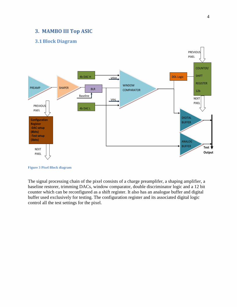
3. MAMBO III Top ASIC
3.1 Block Diagram
PREAMP SHAPER BLR WINDOW
COMPARATOR
4b DAC H
4b DAC L
DDL Logic
COUNTER/
SHIFT
REGISTER
12b
ANALOG
BUFFER
DIGITAL
BUFFER
VthH
VthL Baseline
PREVIOUS
PIXEL
NEXT
PIXEL
Test
Output
Configuration Register -DAC setup (8bits) -Test setup (3bits)
NEXT
PIXEL
PREVIOUS
PIXEL
Figure 3 Pixel Block diagram
The signal processing chain of the pixel consists of a charge preamplifer, a shaping amplifier, a
baseline restorer, trimming DACs, window comparator, double discriminator logic and a 12 bit
counter which can be reconfigured as a shift register. It also has an analogue buffer and digital
buffer used exclusively for testing. The configuration register and its associated digital logic
control all the test settings for the pixel.
5
3.2 Schematics
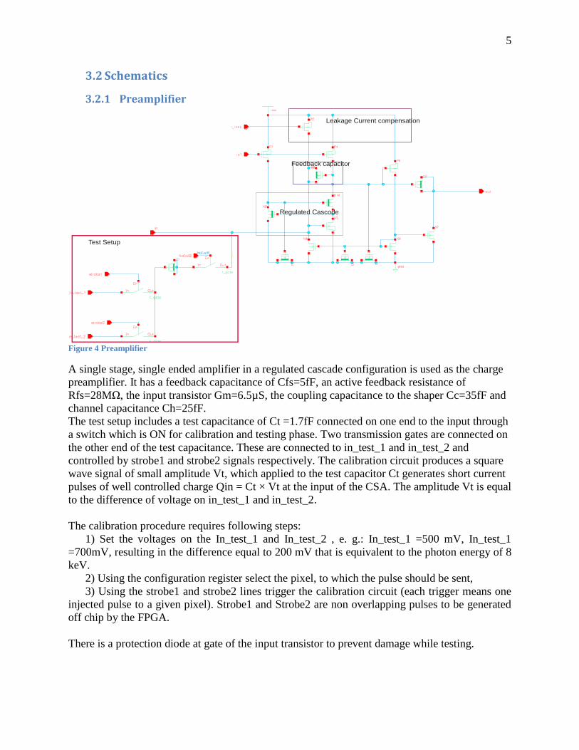
3.2.1 Preamplifier
Regulated Cascode
Leakage Current compensation
Feedback capacitor
Test Setup
Figure 4 Preamplifier
A single stage, single ended amplifier in a regulated cascade configuration is used as the charge
preamplifier. It has a feedback capacitance of Cfs=5fF, an active feedback resistance of
Rfs=28MΩ, the input transistor Gm=6.5µS, the coupling capacitance to the shaper Cc=35fF and
channel capacitance Ch=25fF.
The test setup includes a test capacitance of Ct =1.7fF connected on one end to the input through
a switch which is ON for calibration and testing phase. Two transmission gates are connected on
the other end of the test capacitance. These are connected to in_test_1 and in_test_2 and
controlled by strobe1 and strobe2 signals respectively. The calibration circuit produces a square
wave signal of small amplitude Vt, which applied to the test capacitor Ct generates short current
pulses of well controlled charge Qin = Ct × Vt at the input of the CSA. The amplitude Vt is equal
to the difference of voltage on in_test_1 and in_test_2.
The calibration procedure requires following steps:
1) Set the voltages on the In_test_1 and In_test_2 , e. g.: In_test_1 =500 mV, In_test_1
=700mV, resulting in the difference equal to 200 mV that is equivalent to the photon energy of 8
keV.
2) Using the configuration register select the pixel, to which the pulse should be sent,
3) Using the strobe1 and strobe2 lines trigger the calibration circuit (each trigger means one
injected pulse to a given pixel). Strobe1 and Strobe2 are non overlapping pulses to be generated
off chip by the FPGA.
There is a protection diode at gate of the input transistor to prevent damage while testing.
6
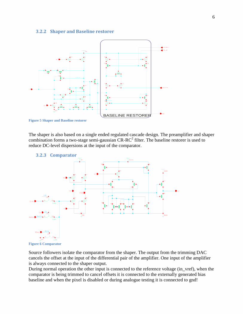
3.2.2 Shaper and Baseline restorer
BASELINE RESTORER Figure 5 Shaper and Baseline restorer
The shaper is also based on a single ended regulated cascade design. The preamplifier and shaper
combination forms a two-stage semi-gaussian CR-RC2 filter. The baseline restorer is used to
reduce DC-level dispersions at the input of the comparator.
3.2.3 Comparator
Figure 6 Comparator
Source followers isolate the comparator from the shaper. The output from the trimming DAC
cancels the offset at the input of the differential pair of the amplifier. One input of the amplifier
is always connected to the shaper output.
During normal operation the other input is connected to the reference voltage (in_vref), when the
comparator is being trimmed to cancel offsets it is connected to the externally generated bias
baseline and when the pixel is disabled or during analogue testing it is connected to gnd!
7
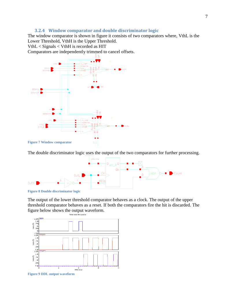
3.2.4 Window comparator and double discriminator logic The window comparator is shown in figure it consists of two comparators where, VthL is the
Lower Threshold, VthH is the Upper Threshold.
VthL < Signals < VthH is recorded as HIT
Comparators are independently trimmed to cancel offsets.
The double discriminator logic uses the output of the two comparators for further processing.
Figure 8 Double discriminator logic
The output of the lower threshold comparator behaves as a clock. The output of the upper
threshold comparator behaves as a reset. If both the comparators fire the hit is discarded. The
figure below shows the output waveform.
Figure 9 DDL output waveform
Figure 7 Window comparator
8
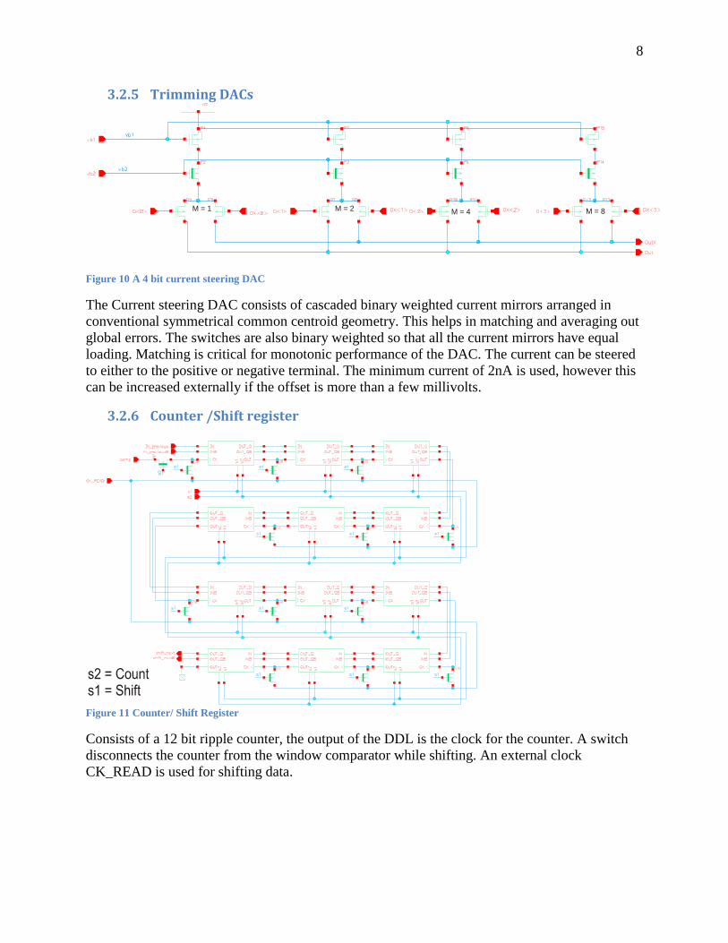
3.2.5 Trimming DACs
M = 1 M = 2 M = 4 M = 8
Figure 10 A 4 bit current steering DAC
The Current steering DAC consists of cascaded binary weighted current mirrors arranged in
conventional symmetrical common centroid geometry. This helps in matching and averaging out
global errors. The switches are also binary weighted so that all the current mirrors have equal
loading. Matching is critical for monotonic performance of the DAC. The current can be steered
to either to the positive or negative terminal. The minimum current of 2nA is used, however this
can be increased externally if the offset is more than a few millivolts.
3.2.6 Counter /Shift register
Figure 11 Counter/ Shift Register
Consists of a 12 bit ripple counter, the output of the DDL is the clock for the counter. A switch
disconnects the counter from the window comparator while shifting. An external clock
CK_READ is used for shifting data.
9
3.2.7 Configuration register and test control logic An 11 bit configuration register is used to setup the
operation of each pixel. The data is input serially as
shown in the figure alongside using the serial clk. It is
then loaded onto a latch using the parallel load signal.
2 x 4bits are used for setting of the two trimming
DACs. The rest 3 bits are used by test control logic to
setup the pixel for the right mode of operation. The
setup configuration for bits b<2:0> is shown in table
below. It consists of a 3-8 bit decoder and additional
combinational logic to control switches.
Figure 12 Configuration register
SETUP
B2
SETUP
B1
SETUP
B0
DAC
H0
DAC
H1
DAC
H2
DAC
H3
DAC
L0
DAC
L1
DAC
L2
DAC
L3
3.2.8 Analog Buffer
The analogue buffer is used only for test purposes hence it is disconnected during normal
operation. Only one pixel can be tested at a time, hence only one analogue buffer is enabled. The
tail current of the buffer is disconnected when it is not in use such that the power consumption of
the ASIC is minimized. SOURCE FOLLOWER
SOURCE FOLLOWER
Figure 13 Analogue buffer
10
Source followers are used for signal conditioning. The buffer is a single stage amplifier with
10µA of tail current. It has a gain of about 50dB.
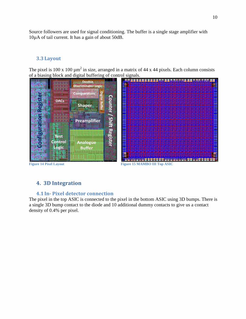
3.3 Layout
The pixel is 100 x 100 µm2 in size, arranged in a matrix of 44 x 44 pixels. Each column consists
of a biasing block and digital buffering of control signals.
Figure 14 Pixel Layout
Figure 15 MAMBO III Top ASIC
4. 3D Integration
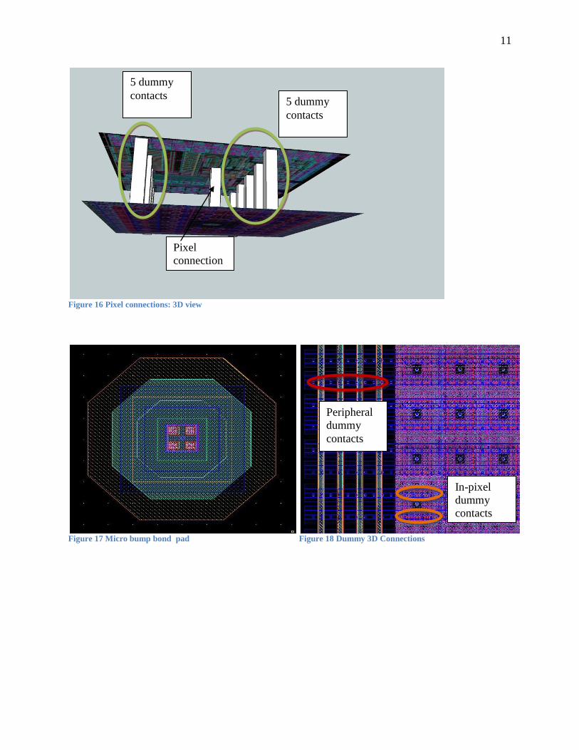
4.1 In- Pixel detector connection The pixel in the top ASIC is connected to the pixel in the bottom ASIC using 3D bumps. There is
a single 3D bump contact to the diode and 10 additional dummy contacts to give us a contact
density of 0.4% per pixel.
11
Figure 16 Pixel connections: 3D view
Figure 17 Micro bump bond pad
Figure 18 Dummy 3D Connections
In-pixel
dummy
contacts
Peripheral
dummy
contacts
5 dummy
contacts
5 dummy
contacts
Pixel
connection
12
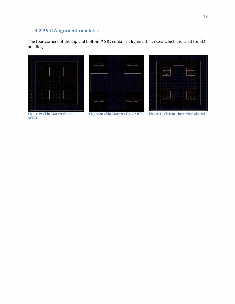
4.2 ASIC Alignment markers
The four corners of the top and bottom ASIC contains alignment markers which are used for 3D
bonding.
Figure 19 Chip Marker (Bottom
ASIC)
Figure 20 Chip Marker (Top ASIC)
Figure 21 Chip markers when aligned
13
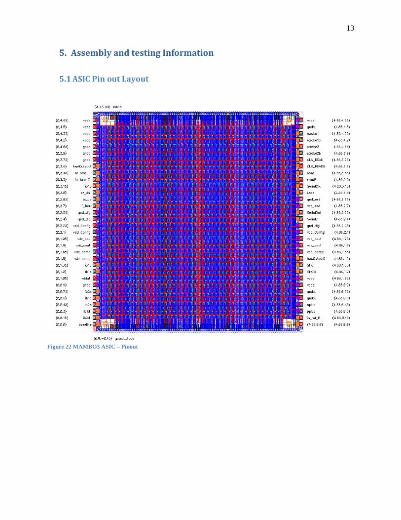
5. Assembly and testing Information
5.1 ASIC Pin out Layout
Figure 22 MAMBO3 ASIC – Pinout
14
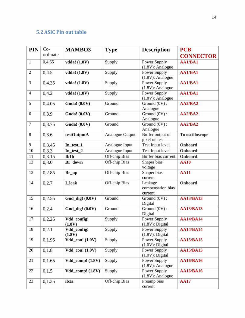
5.2 ASIC Pin out table
PIN Co-
ordinate MAMBO3 Type Description PCB
CONNECTOR 1 0,4.65 vdda! (1.8V) Supply Power Supply
(1.8V): Analogue
AA1/BA1
2 0,4.5 vdda! (1.8V) Supply Power Supply
(1.8V): Analogue
AA1/BA1
3 0,4.35 vdda! (1.8V) Supply Power Supply
(1.8V): Analogue
AA1/BA1
4 0,4.2 vdda! (1.8V) Supply Power Supply
(1.8V): Analogue
AA1/BA1
5 0,4.05 Gnda! (0.0V) Ground Ground (0V) :
Analogue
AA2/BA2
6 0,3.9 Gnda! (0.0V) Ground Ground (0V) :
Analogue
AA2/BA2
7 0,3.75 Gnda! (0.0V) Ground Ground (0V) :
Analogue
AA2/BA2
8 0,3.6 testOutputA Analogue Output Buffer output of
pixel on test To oscilloscope
9 0,3.45 In_test_1 Analogue Input Test Input level Onboard
10 0,3.3 In_test_2 Analogue Input Test Input level Onboard
11 0,3.15 Ib1b Off-chip Bias Buffer bias current Onboard
12 0,3.0 Br_down Off-chip Bias Shaper bias
voltage AA10
13 0,2.85 Br_up Off-chip Bias Shaper bias
current AA11
14 0,2.7 I_leak Off-chip Bias Leakage
compensation bias
current
Onboard
15 0,2.55 Gnd_dig! (0.0V) Ground Ground (0V) :
Digital AA13/BA13
16 0,2.4 Gnd_dig! (0.0V) Ground Ground (0V) :
Digital AA13/BA13
17 0,2.25 Vdd_config!
(1.8V)
Supply Power Supply
(1.8V): Digital AA14/BA14
18 0,2.1 Vdd_config!
(1.8V)
Supply Power Supply
(1.8V): Digital AA14/BA14
19 0,1.95 Vdd_cou! (1.0V) Supply Power Supply
(1.0V): Digital AA15/BA15
20 0,1.8 Vdd_cou! (1.0V) Supply Power Supply
(1.0V): Digital AA15/BA15
21 0,1.65 Vdd_comp! (1.8V) Supply Power Supply
(1.8V): Analogue
AA16/BA16
22 0,1.5 Vdd_comp! (1.8V) Supply Power Supply
(1.8V): Analogue
AA16/BA16
23 0,1.35 ib1a Off-chip Bias Preamp bias
current AA17
15
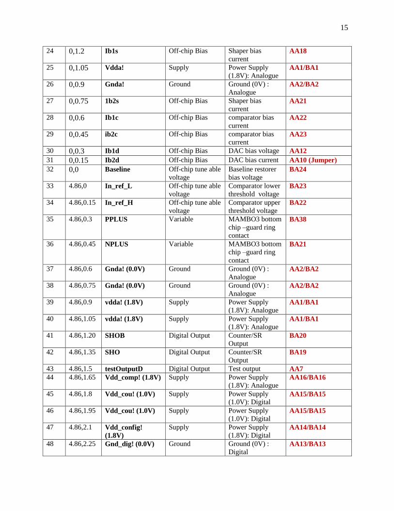
24 0,1.2 Ib1s Off-chip Bias Shaper bias
current AA18
25 0,1.05 Vdda! Supply Power Supply
(1.8V): Analogue
AA1/BA1
26 0,0.9 Gnda! Ground Ground (0V) :
Analogue
AA2/BA2
27 0,0.75 1b2s Off-chip Bias Shaper bias
current AA21
28 0,0.6 Ib1c Off-chip Bias comparator bias
current AA22
29 0,0.45 ib2c Off-chip Bias comparator bias
current AA23
30 0,0.3 Ib1d Off-chip Bias DAC bias voltage AA12
31 0,0.15 Ib2d Off-chip Bias DAC bias current AA10 (Jumper)
32 0,0 Baseline Off-chip tune able
voltage
Baseline restorer
bias voltage BA24
33 4.86,0 In_ref_L Off-chip tune able
voltage
Comparator lower
threshold voltage BA23
34 4.86,0.15 In_ref_H Off-chip tune able
voltage
Comparator upper
threshold voltage BA22
35 4.86,0.3 PPLUS Variable MAMBO3 bottom
chip –guard ring
contact
BA38
36 4.86,0.45 NPLUS Variable MAMBO3 bottom
chip –guard ring
contact
BA21
37 4.86,0.6 Gnda! (0.0V) Ground Ground (0V) :
Analogue
AA2/BA2
38 4.86,0.75 Gnda! (0.0V) Ground Ground (0V) :
Analogue
AA2/BA2
39 4.86,0.9 vdda! (1.8V) Supply Power Supply
(1.8V): Analogue
AA1/BA1
40 4.86,1.05 vdda! (1.8V) Supply Power Supply
(1.8V): Analogue
AA1/BA1
41 4.86,1.20 SHOB Digital Output Counter/SR
Output BA20
42 4.86,1.35 SHO Digital Output Counter/SR
Output BA19
43 4.86,1.5 testOutputD Digital Output Test output AA7
44 4.86,1.65 Vdd_comp! (1.8V) Supply Power Supply
(1.8V): Analogue
AA16/BA16
45 4.86,1.8 Vdd_cou! (1.0V) Supply Power Supply
(1.0V): Digital AA15/BA15
46 4.86,1.95 Vdd_cou! (1.0V) Supply Power Supply
(1.0V): Digital AA15/BA15
47 4.86,2.1 Vdd_config!
(1.8V)
Supply Power Supply
(1.8V): Digital AA14/BA14
48 4.86,2.25 Gnd_dig! (0.0V) Ground Ground (0V) :
Digital AA13/BA13
16
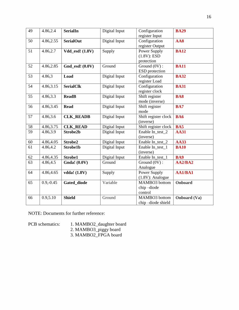
49 4.86,2.4 SerialIn Digital Input Configuration
register Input BA29
50 4.86,2.55 SerialOut Digital Input Configuration
register Output AA8
51 4.86,2.7 Vdd_esd! (1.8V) Supply Power Supply
(1.8V): ESD
protection
BA12
52 4.86,2.85 Gnd_esd! (0.0V) Ground Ground (0V) :
ESD protection
BA11
53 4.86,3 Load Digital Input Configuration
register Load
BA32
54 4.86,3.15 SerialClk Digital Input Configuration
register clock
BA31
55 4.86,3.3 ReadB Digital Input Shift register
mode (inverse) BA8
56 4.86,3.45 Read Digital Input Shift register
mode BA7
57 4.86,3.6 CLK_READB Digital Input Shift register clock
(inverse) BA6
58 4.86,3.75 CLK_READ Digital Input Shift register clock BA5
59 4.86,3.9 Strobe2b Digital Input Enable In_test_2
(inverse) AA31
60 4.86,4.05 Strobe2 Digital Input Enable In_test_2 AA33
61 4.86,4.2 Strobe1b Digital Input Enable In_test_1
(inverse) BA10
62 4.86,4.35 Strobe1 Digital Input Enable In_test_1 BA9
63 4.86,4.5 Gnda! (0.0V) Ground Ground (0V) :
Analogue
AA2/BA2
64 4.86,4.65 vdda! (1.8V) Supply Power Supply
(1.8V): Analogue
AA1/BA1
65 0.9,-0.45 Gated_diode Variable MAMBO3 bottom
chip –diode
control
Onboard
66 0.9,5.10 Shield Ground MAMBO3 bottom
chip –diode shield
Onboard (Va)
NOTE: Documents for further reference:
PCB schematics: 1. MAMBO2_daughter board
2. MAMBO3_piggy board
3. MAMBO2_FPGA board
17
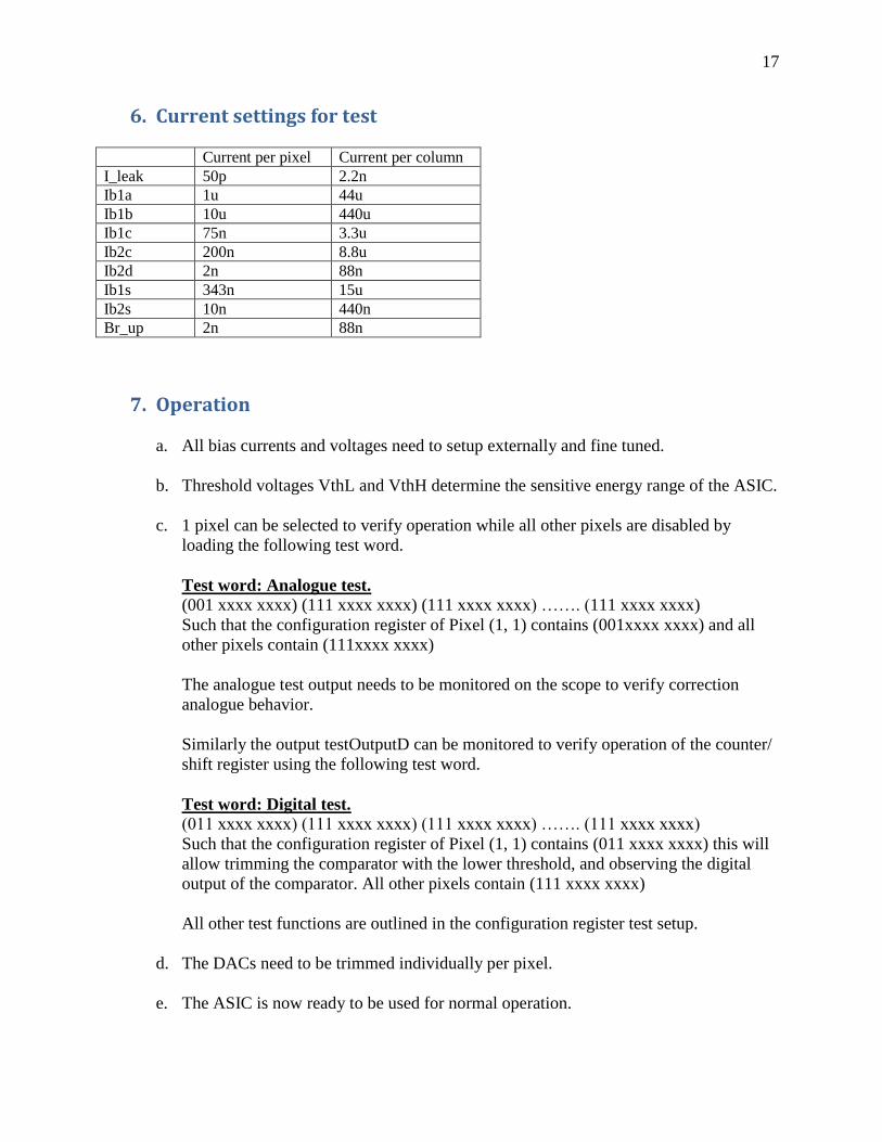
6. Current settings for test Current per pixel Current per column
I_leak 50p 2.2n
Ib1a 1u 44u
Ib1b 10u 440u
Ib1c 75n 3.3u
Ib2c 200n 8.8u
Ib2d 2n 88n
Ib1s 343n 15u
Ib2s 10n 440n
Br_up 2n 88n
7. Operation
a. All bias currents and voltages need to setup externally and fine tuned.
b. Threshold voltages VthL and VthH determine the sensitive energy range of the ASIC.
c. 1 pixel can be selected to verify operation while all other pixels are disabled by
loading the following test word.
Test word: Analogue test.
(001 xxxx xxxx) (111 xxxx xxxx) (111 xxxx xxxx) ……. (111 xxxx xxxx)
Such that the configuration register of Pixel (1, 1) contains (001xxxx xxxx) and all
other pixels contain (111xxxx xxxx)
The analogue test output needs to be monitored on the scope to verify correction
analogue behavior.
Similarly the output testOutputD can be monitored to verify operation of the counter/
shift register using the following test word.
Test word: Digital test.
(011 xxxx xxxx) (111 xxxx xxxx) (111 xxxx xxxx) ……. (111 xxxx xxxx)
Such that the configuration register of Pixel (1, 1) contains (011 xxxx xxxx) this will
allow trimming the comparator with the lower threshold, and observing the digital
output of the comparator. All other pixels contain (111 xxxx xxxx)
All other test functions are outlined in the configuration register test setup.
d. The DACs need to be trimmed individually per pixel.
e. The ASIC is now ready to be used for normal operation.
18
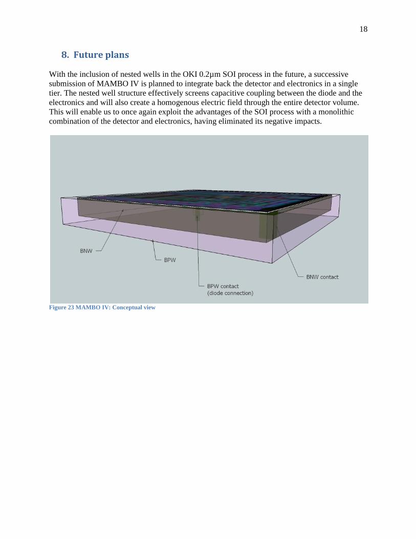
8. Future plans
With the inclusion of nested wells in the OKI 0.2µm SOI process in the future, a successive
submission of MAMBO IV is planned to integrate back the detector and electronics in a single
tier. The nested well structure effectively screens capacitive coupling between the diode and the
electronics and will also create a homogenous electric field through the entire detector volume.
This will enable us to once again exploit the advantages of the SOI process with a monolithic
combination of the detector and electronics, having eliminated its negative impacts.
Figure 23 MAMBO IV: Conceptual view