making qsys components tutorial - brown...
TRANSCRIPT

Making Qsys Components
For Quartus II 12.0
1 Introduction
The Altera Qsys tool allows a digital system to be designed by interconnecting selected Qsys components, such asprocessors, memory controllers, parallel and serial ports, and the like. The Qsys tool includes many pre-designedcomponents that may be selected for inclusion in a designed system, and it is also possible for users to createtheir own custom Qsys components. This tutorial provides an introduction to the process of creating custom Qsyscomponents. The discussion is based on the assumption that the reader is familiar with the Verilog or VHDLhardware description language and is also familiar with the material in the tutorial Introduction to the Altera QsysSystem Integration Tool.
The screen captures in this tutorial were obtained using the Quartus II version 12.0 software; if other versions areused, some of the images may be slightly different.
Contents:
• Introduction to Qsys
• What is a Qsys component?
• Avalon Memory-Mapped Interface details
• Adding a new component to Qsys
• Instantiating the new component
Altera Corporation - University ProgramAugust 2012
1

MAKING QSYS COMPONENTS For Quartus II 12.0
2 Introduction to Qsys
The Qsys tool allows users to put together a system using pre-made and/or custom components. Such systemsusually comprise one or more processors, memory interfaces, I/O ports and other custom hardware. The Qsys-created system can be included as part of a larger circuit and implemented on an FPGA board, such as the AlteraDE-series boards. An example of such a system is depicted in Figure 1, where the part of the system created by theQsys tool is highlighted in a blue color.
Serial port
Slider
Nios II processorJTAG port
LEDs7-Segment
On-chipmemory
Expansionconnectors
System
Host computer(USB connection)
RS-232chip
USBBlaster
Altera DE-series Board
ID
timerInterval
Reset
KEY
FPGA chip
Parallelports
Parallelport
Parallelports
Parallelport
Pushbuttons
Parallelport
SRAMchip
SDRAMchip
SRAMcontroller
SDRAMcontroller
Avalon Interconnect
displaysswitches
Figure 1. Block diagram of an example Qsys system implemented on an FPGA board.
Each component in the system, referred to as a Qsys component, adheres to at least one of the Avalon Interfacessupported by Qsys. With the interface defined for the component, Qsys is able to construct an interconnect structure,called the Avalon Interconnect, which enables components to exchange data. The Qsys tool can generate a systembased on the selected set of components and user parameters. The generated system contains Verilog or VHDL codefor each component and the interconnect structure, allowing it to be synthesized, placed and routed for an FPGAdevice.
2 Altera Corporation - University ProgramAugust 2012
MAKING QSYS COMPONENTS For Quartus II 12.0
In this tutorial we explain what we mean by a Qsys component, describe the Avalon Interfaces in more detail, andshow how to create a custom component that can be included in the Qsys list of available components.
3 What is a Qsys Component?
A Qsys component is a hardware subcircuit that is available as a library component for use in the Qsys tool. Typically,the contains two parts: the internal hardware modules, and the external Avalon Interfaces. The internal modules arethe circuits that implement the desired functionality of the Qsys component, while the Avalon Interfaces are used bythe component to communicate with hardware modules that are external to the component.
There are many types of Avalon Interfaces; the most commonly used types are:
• Avalon Clock Interface – an interface that drives or receives clocks
• Avalon Reset Interface – an interface that provides reset capability
• Avalon Memory-Mapped Interface (Avalon MM) – an address-based read/write interface which is typical ofmaster-slave connections
• Avalon Streaming Interface (Avalon-ST) – an interface that supports unidirectional flow of data
• Avalon Conduit Interface – an interface that accommodates individual signals or groups of signals that donot fit into any of the other Avalon Interface types. You can export the conduit signals to make connectionsexternal to the Qsys system.
A single component can use as many of these interface types as it requires. For example, a component might providean Avalon-ST port for high-throughput data, in addition to an Avalon MM slave port for control. All componentsmust include the Avalon Clock and Reset Interfaces. Readers interested in more complete information about theAvalon Interfaces may consult the Avalon Interface Specifications document that can be found on the Altera website.
In this tutorial we will show how to develop a Qsys component that has an Avalon Memory-Mapped Interface andan Avalon Conduit Interface. The component is a 16-bit register that can be read or written as a memory-mappedslave device via the Avalon Interconnect and can be visible outside the system through a conduit signal. The purposeof the conduit is to allow the register contents to displayed on external components such as LEDs or 7-segmentdisplays. Thus, this register is similar to the output parallel ports shown in Figure 1.
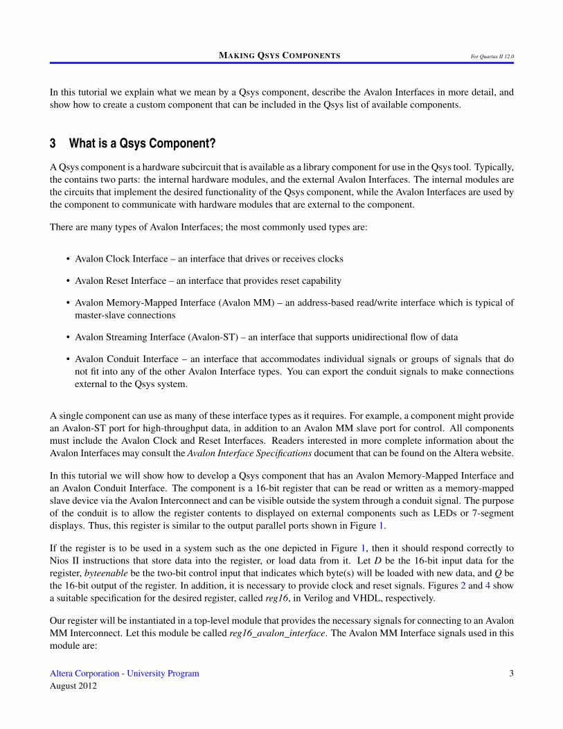
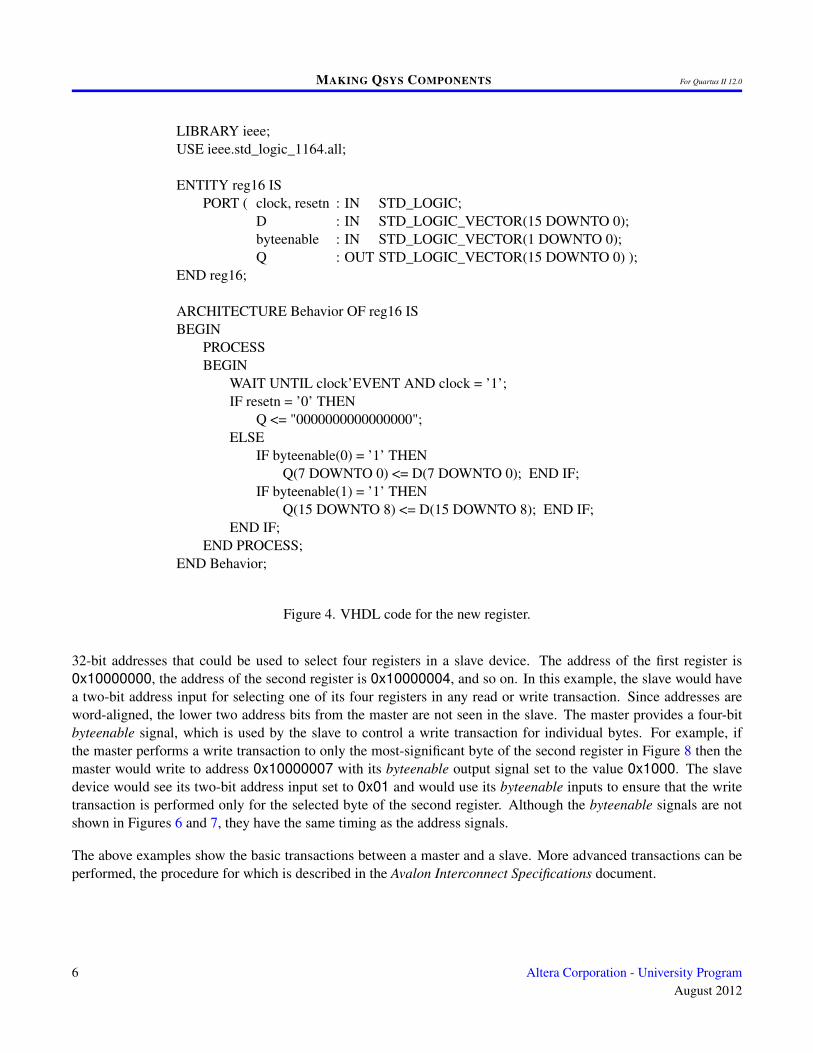
If the register is to be used in a system such as the one depicted in Figure 1, then it should respond correctly toNios II instructions that store data into the register, or load data from it. Let D be the 16-bit input data for theregister, byteenable be the two-bit control input that indicates which byte(s) will be loaded with new data, and Q bethe 16-bit output of the register. In addition, it is necessary to provide clock and reset signals. Figures 2 and 4 showa suitable specification for the desired register, called reg16, in Verilog and VHDL, respectively.
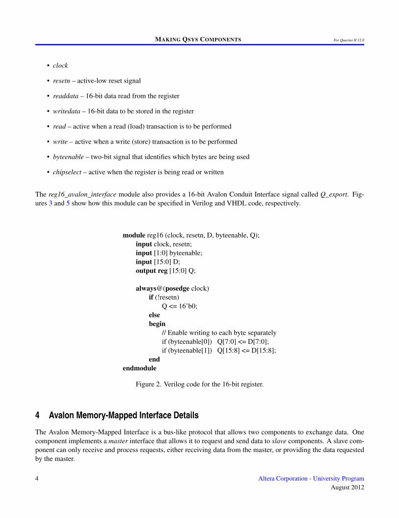
Our register will be instantiated in a top-level module that provides the necessary signals for connecting to an AvalonMM Interconnect. Let this module be called reg16_avalon_interface. The Avalon MM Interface signals used in thismodule are:
Altera Corporation - University ProgramAugust 2012
3
MAKING QSYS COMPONENTS For Quartus II 12.0
• clock
• resetn – active-low reset signal
• readdata – 16-bit data read from the register
• writedata – 16-bit data to be stored in the register
• read – active when a read (load) transaction is to be performed
• write – active when a write (store) transaction is to be performed
• byteenable – two-bit signal that identifies which bytes are being used
• chipselect – active when the register is being read or written
The reg16_avalon_interface module also provides a 16-bit Avalon Conduit Interface signal called Q_export. Fig-ures 3 and 5 show how this module can be specified in Verilog and VHDL code, respectively.
module reg16 (clock, resetn, D, byteenable, Q);input clock, resetn;input [1:0] byteenable;input [15:0] D;output reg [15:0] Q;
always@(posedge clock)if (!resetn)
Q <= 16’b0;elsebegin
// Enable writing to each byte separatelyif (byteenable[0]) Q[7:0] <= D[7:0];if (byteenable[1]) Q[15:8] <= D[15:8];
endendmodule
Figure 2. Verilog code for the 16-bit register.
4 Avalon Memory-Mapped Interface Details
The Avalon Memory-Mapped Interface is a bus-like protocol that allows two components to exchange data. Onecomponent implements a master interface that allows it to request and send data to slave components. A slave com-ponent can only receive and process requests, either receiving data from the master, or providing the data requestedby the master.
4 Altera Corporation - University ProgramAugust 2012
MAKING QSYS COMPONENTS For Quartus II 12.0
module reg16_avalon_interface (clock, resetn, writedata, readdata, write, read,byteenable, chipselect, Q_export);
// signals for connecting to the Avalon fabricinput clock, resetn, read, write, chipselect;input [1:0] byteenable;input [15:0] writedata;output [15:0] readdata;
// signal for exporting register contents outside of the embedded systemoutput [15:0] Q_export;
wire [1:0] local_byteenable;wire [15:0] to_reg, from_reg;
assign to_reg = writedata;
assign local_byteenable = (chipselect & write) ? byteenable : 2’d0;
reg16 U1 ( .clock(clock), .resetn(resetn), .D(to_reg), .byteenable(local_byteenable),.Q(from_reg) );
assign readdata = from_reg;assign Q_export = from_reg;
endmodule
Figure 3. Verilog code for the Avalon MM Interface.
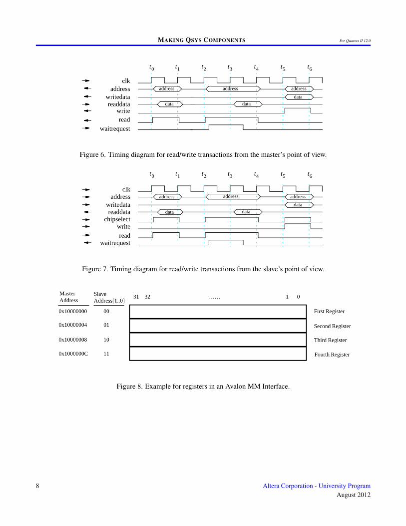
Each slave device includes one or more registers that can be accessed for read or write transaction by a masterdevice. Figures 6 and 7 illustrate the signals that are used by master and slave interfaces. The direction of eachsignal is indicated by arrows beside it, with ← indicating an output and → indicating an input to a device. Alltransactions are synchronized to the positive edge of the Avalon clk signal. At time t0 in the figures, the masterbegins a read transaction by placing a valid address on its address outputs and asserting its read control signal. Theslave recognizes the request because its chipselect input is asserted. It responds by placing valid data on its readdataoutputs; the master captures this data on its readdata inputs and the read transaction ends at time t1. A second readtransaction is shown in the figure starting at time t2. In this case, the slave device asserts the waitrequest input of themaster, which can be used to extend a read transaction by any number of clock cycles. The slave device deassertsthe waitrequest signal and provides the requested data at time t3, and the read transaction ends at time t4.
A write transaction is illustrated starting at time t5 in Figures 6 and 7. The master places a valid address and data onits address and datawrite outputs, and asserts the write control signal. The slave captures the data on its datawriteinputs and the write transaction ends at time t6. Although not shown in this example, a slave device can assert thewaitrequest input of the master to extend a write transaction over multiple clock cycles if needed.
Addresses used by master devices are aligned to 32-bit word boundaries. For example, Figure 8 illustrates four
Altera Corporation - University ProgramAugust 2012
5
MAKING QSYS COMPONENTS For Quartus II 12.0
LIBRARY ieee;USE ieee.std_logic_1164.all;
ENTITY reg16 ISPORT ( clock, resetn : IN STD_LOGIC;
D : IN STD_LOGIC_VECTOR(15 DOWNTO 0);byteenable : IN STD_LOGIC_VECTOR(1 DOWNTO 0);Q : OUT STD_LOGIC_VECTOR(15 DOWNTO 0) );
END reg16;
ARCHITECTURE Behavior OF reg16 ISBEGIN
PROCESSBEGIN
WAIT UNTIL clock’EVENT AND clock = ’1’;IF resetn = ’0’ THEN
Q <= "0000000000000000";ELSE
IF byteenable(0) = ’1’ THENQ(7 DOWNTO 0) <= D(7 DOWNTO 0); END IF;
IF byteenable(1) = ’1’ THENQ(15 DOWNTO 8) <= D(15 DOWNTO 8); END IF;
END IF;END PROCESS;
END Behavior;
Figure 4. VHDL code for the new register.
32-bit addresses that could be used to select four registers in a slave device. The address of the first register is0x10000000, the address of the second register is 0x10000004, and so on. In this example, the slave would havea two-bit address input for selecting one of its four registers in any read or write transaction. Since addresses areword-aligned, the lower two address bits from the master are not seen in the slave. The master provides a four-bitbyteenable signal, which is used by the slave to control a write transaction for individual bytes. For example, ifthe master performs a write transaction to only the most-significant byte of the second register in Figure 8 then themaster would write to address 0x10000007 with its byteenable output signal set to the value 0x1000. The slavedevice would see its two-bit address input set to 0x01 and would use its byteenable inputs to ensure that the writetransaction is performed only for the selected byte of the second register. Although the byteenable signals are notshown in Figures 6 and 7, they have the same timing as the address signals.
The above examples show the basic transactions between a master and a slave. More advanced transactions can beperformed, the procedure for which is described in the Avalon Interconnect Specifications document.
6 Altera Corporation - University ProgramAugust 2012

MAKING QSYS COMPONENTS For Quartus II 12.0
LIBRARY ieee;USE ieee.std_logic_1164.all;
ENTITY reg16_avalon_interface ISPORT ( clock, resetn : IN STD_LOGIC;
read, write, chipselect : IN STD_LOGIC;writedata : IN STD_LOGIC_VECTOR(15 DOWNTO 0);byteenable : IN STD_LOGIC_VECTOR(1 DOWNTO 0);readdata : OUT STD_LOGIC_VECTOR(15 DOWNTO 0);Q_export : OUT STD_LOGIC_VECTOR(15 DOWNTO 0) );
END reg16_avalon_interface;
ARCHITECTURE Structure OF reg16_avalon_interface ISSIGNAL local_byteenable : STD_LOGIC_VECTOR(1 DOWNTO 0);SIGNAL to_reg, from_reg : STD_LOGIC_VECTOR(15 DOWNTO 0);
COMPONENT reg16PORT ( clock, resetn : IN STD_LOGIC;
D : IN STD_LOGIC_VECTOR(15 DOWNTO 0);byteenable : IN STD_LOGIC_VECTOR(1 DOWNTO 0);Q : OUT STD_LOGIC_VECTOR(15 DOWNTO 0) );
END COMPONENT;BEGIN
to_reg <= writedata;WITH (chipselect AND write) SELECT
local_byteenable <= byteenable WHEN ’1’, "00" WHEN OTHERS;reg_instance: reg16 PORT MAP (clock, resetn, to_reg, local_byteenable, from_reg);readdata <= from_reg;Q_export <= from_reg;
END Structure;
Figure 5. VHDL code for the memory-mapped new-register interface.
Altera Corporation - University ProgramAugust 2012
7
MAKING QSYS COMPONENTS For Quartus II 12.0
clkaddress
writedatareaddata
chipselectwrite
readwaitrequest
datadata
address address
clkaddress
writedatareaddata
writeread
waitrequest
datadata
address address
data
address
t0 t1 t2 t4 t5 t6t3
data
address
t0 t1 t2 t4 t5 t6t3
Figure 6. Timing diagram for read/write transactions from the master’s point of view.
clkaddress
writedatareaddata
chipselectwrite
readwaitrequest
datadata
address address
clkaddress
writedatareaddata
writeread
waitrequest
datadata
address address
data
address
t0 t1 t2 t4 t5 t6t3
data
address
t0 t1 t2 t4 t5 t6t3
Figure 7. Timing diagram for read/write transactions from the slave’s point of view.
1
31 32 …… 1 0
First Register
Second Register
Third Register
Fourth Register
00
01
10
11
0x10000000
0x10000004
0x10000008
0x1000000C
Master Address
Slave Address[1..0]
Figure 8. Example for registers in an Avalon MM Interface.
8 Altera Corporation - University ProgramAugust 2012
MAKING QSYS COMPONENTS For Quartus II 12.0
5 Adding a New Component to the Qsys Component Library
In this section we show how to create a new Qsys component for our 16-bit register defined in Figures 2 to 5.As a first step, start the Quartus II software and make a new project for use with this tutorial. Name the projectcomponent_tutorial, and choose the settings that are needed for your DE-series board, including the specific FPGAchip.
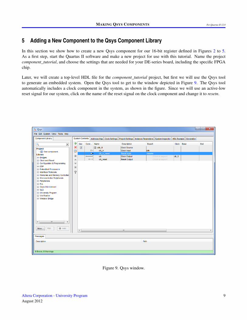
Later, we will create a top-level HDL file for the component_tutorial project, but first we will use the Qsys toolto generate an embedded system. Open the Qsys tool to get to the window depicted in Figure 9. The Qsys toolautomatically includes a clock component in the system, as shown in the figure. Since we will use an active-lowreset signal for our system, click on the name of the reset signal on the clock component and change it to resetn.
Figure 9. Qsys window.
Altera Corporation - University ProgramAugust 2012
9
MAKING QSYS COMPONENTS For Quartus II 12.0
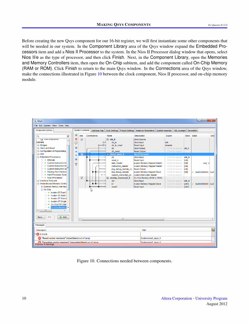
Before creating the new Qsys component for our 16-bit register, we will first instantiate some other components thatwill be needed in our system. In the Component Library area of the Qsys window expand the Embedded Pro-cessors item and add a Nios II Processor to the system. In the Nios II Processor dialog window that opens, selectNios II/e as the type of processor, and then click Finish. Next, in the Component Library, open the Memoriesand Memory Controllers item, then open the On-Chip subitem, and add the component called On-Chip Memory(RAM or ROM). Click Finish to return to the main Qsys window. In the Connections area of the Qsys window,make the connections illustrated in Figure 10 between the clock component, Nios II processor, and on-chip memorymodule.
Figure 10. Connections needed between components.
10 Altera Corporation - University ProgramAugust 2012
MAKING QSYS COMPONENTS For Quartus II 12.0
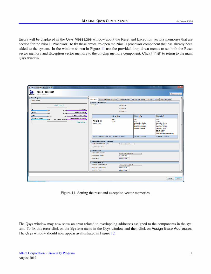
Errors will be displayed in the Qsys Messages window about the Reset and Exception vectors memories that areneeded for the Nios II Processor. To fix these errors, re-open the Nios II processor component that has already beenadded to the system. In the window shown in Figure 11 use the provided drop-down menus to set both the Resetvector memory and Exception vector memory to the on-chip memory component. Click Finish to return to the mainQsys window.
Figure 11. Setting the reset and exception vector memories.
The Qsys window may now show an error related to overlapping addresses assigned to the components in the sys-tem. To fix this error click on the System menu in the Qsys window and then click on Assign Base Addresses.The Qsys window should now appear as illustrated in Figure 12.
Altera Corporation - University ProgramAugust 2012
11

MAKING QSYS COMPONENTS For Quartus II 12.0
Figure 12. The base Qsys system.
12 Altera Corporation - University ProgramAugust 2012
MAKING QSYS COMPONENTS For Quartus II 12.0
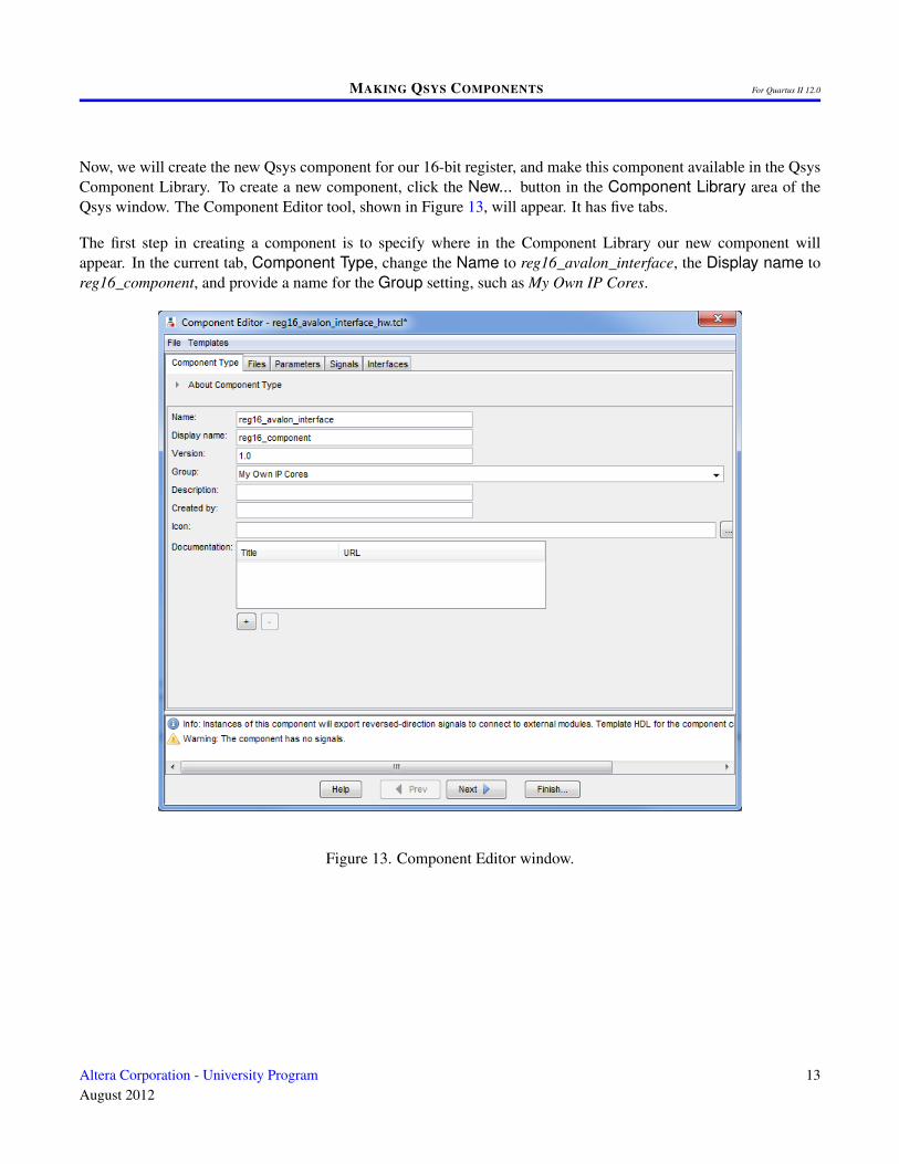
Now, we will create the new Qsys component for our 16-bit register, and make this component available in the QsysComponent Library. To create a new component, click the New... button in the Component Library area of theQsys window. The Component Editor tool, shown in Figure 13, will appear. It has five tabs.
The first step in creating a component is to specify where in the Component Library our new component willappear. In the current tab, Component Type, change the Name to reg16_avalon_interface, the Display name toreg16_component, and provide a name for the Group setting, such as My Own IP Cores.
Figure 13. Component Editor window.
Altera Corporation - University ProgramAugust 2012
13
MAKING QSYS COMPONENTS For Quartus II 12.0
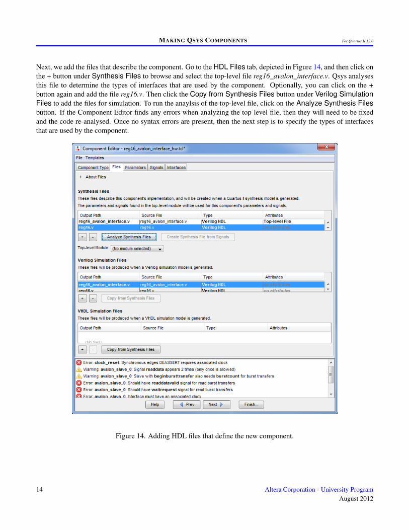
Next, we add the files that describe the component. Go to the HDL Files tab, depicted in Figure 14, and then click onthe + button under Synthesis Files to browse and select the top-level file reg16_avalon_interface.v. Qsys analysesthis file to determine the types of interfaces that are used by the component. Optionally, you can click on the +button again and add the file reg16.v. Then click the Copy from Synthesis Files button under Verilog SimulationFiles to add the files for simulation. To run the anaylsis of the top-level file, click on the Analyze Synthesis Filesbutton. If the Component Editor finds any errors when analyzing the top-level file, then they will need to be fixedand the code re-analysed. Once no syntax errors are present, then the next step is to specify the types of interfacesthat are used by the component.
Figure 14. Adding HDL files that define the new component.
14 Altera Corporation - University ProgramAugust 2012

MAKING QSYS COMPONENTS For Quartus II 12.0
Click on the Signals tab to specify the meaning of each interface port in the top-level entity. This leads to thewindow in Figure 15.
Figure 15. Initial settings for component signals.
Altera Corporation - University ProgramAugust 2012
15
MAKING QSYS COMPONENTS For Quartus II 12.0
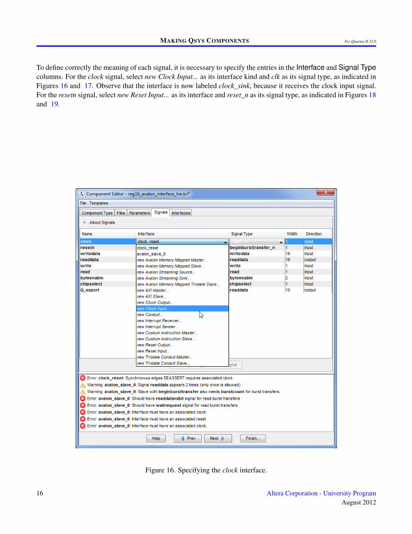
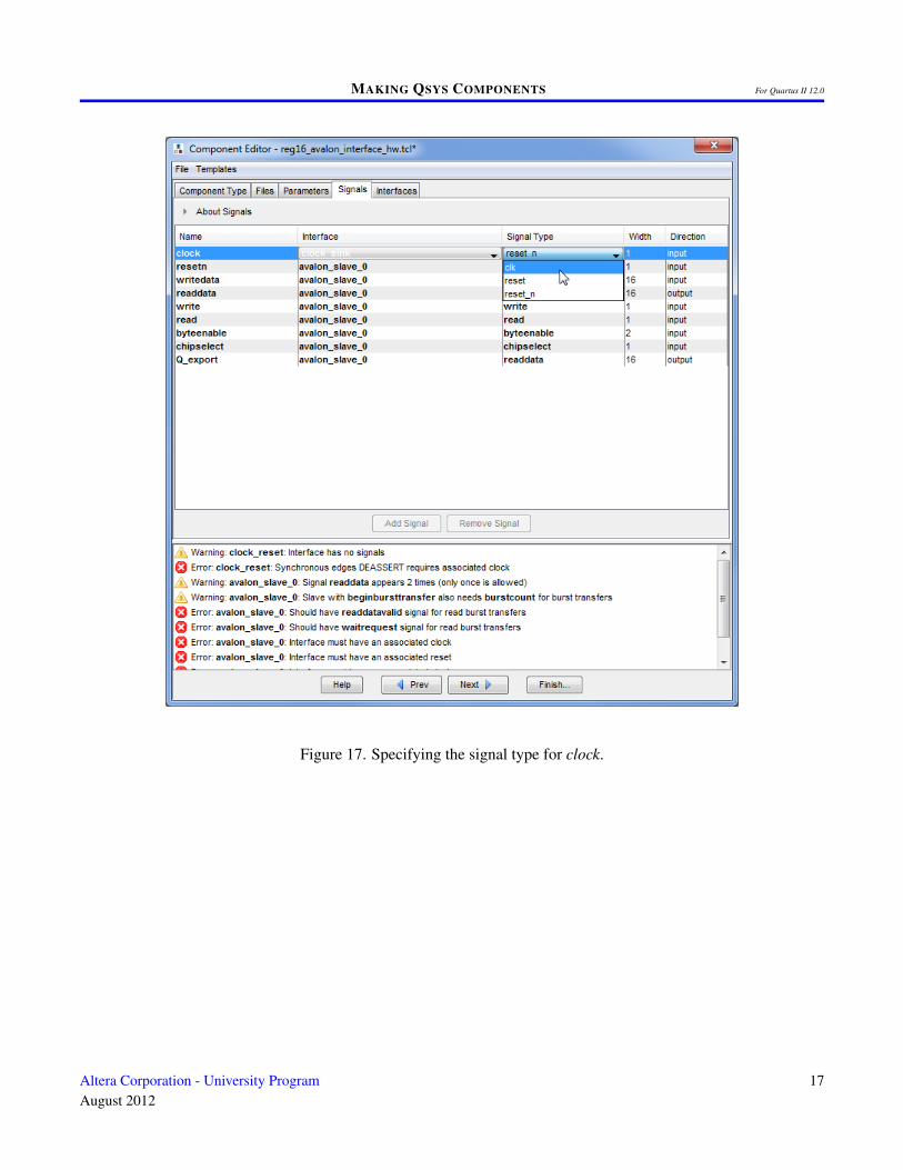
To define correctly the meaning of each signal, it is necessary to specify the entries in the Interface and Signal Typecolumns. For the clock signal, select new Clock Input... as its interface kind and clk as its signal type, as indicated inFigures 16 and 17. Observe that the interface is now labeled clock_sink, because it receives the clock input signal.For the resetn signal, select new Reset Input... as its interface and reset_n as its signal type, as indicated in Figures 18and 19.
Figure 16. Specifying the clock interface.
16 Altera Corporation - University ProgramAugust 2012
MAKING QSYS COMPONENTS For Quartus II 12.0
Figure 17. Specifying the signal type for clock.
Altera Corporation - University ProgramAugust 2012
17

MAKING QSYS COMPONENTS For Quartus II 12.0
Figure 18. Specifying the resetn interface.
18 Altera Corporation - University ProgramAugust 2012

MAKING QSYS COMPONENTS For Quartus II 12.0
Figure 19. Specifying the signal type for resetn.
Altera Corporation - University ProgramAugust 2012
19
MAKING QSYS COMPONENTS For Quartus II 12.0
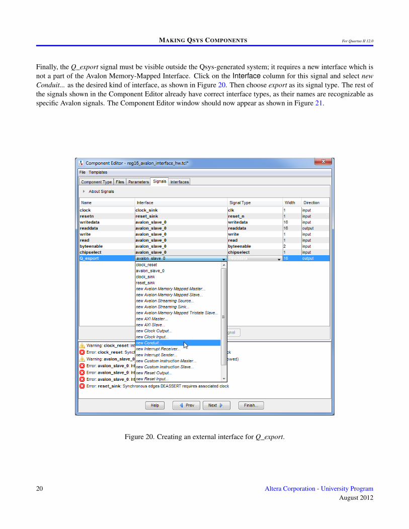
Finally, the Q_export signal must be visible outside the Qsys-generated system; it requires a new interface which isnot a part of the Avalon Memory-Mapped Interface. Click on the Interface column for this signal and select newConduit... as the desired kind of interface, as shown in Figure 20. Then choose export as its signal type. The rest ofthe signals shown in the Component Editor already have correct interface types, as their names are recognizable asspecific Avalon signals. The Component Editor window should now appear as shown in Figure 21.
Figure 20. Creating an external interface for Q_export.
20 Altera Corporation - University ProgramAugust 2012
MAKING QSYS COMPONENTS For Quartus II 12.0
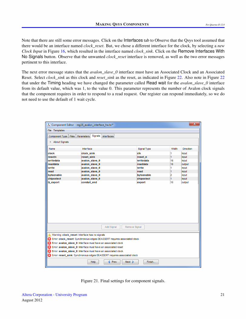
Note that there are still some error messages. Click on the Interfaces tab to Observe that the Qsys tool assumed thatthere would be an interface named clock_reset. But, we chose a different interface for the clock, by selecting a newClock Input in Figure 16, which resulted in the interface named clock_sink. Click on the Remove Interfaces WithNo Signals button. Observe that the unwanted clock_reset interface is removed, as well as the two error messagespertinent to this interface.
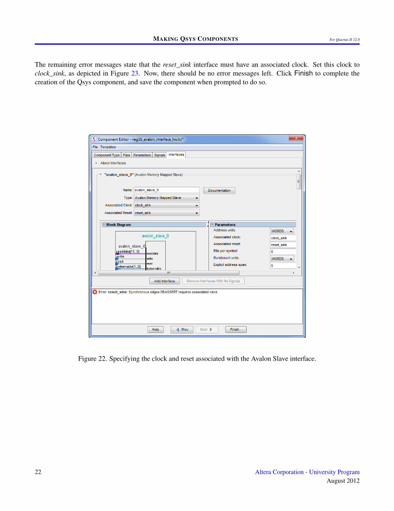
The next error message states that the avalon_slave_0 interface must have an Associated Clock and an AssociatedReset. Select clock_sink as this clock and reset_sink as the reset, as indicated in Figure 22. Also note in Figure 22that under the Timing heading we have changed the parameter called Read wait for the avalon_slave_0 interfacefrom its default value, which was 1, to the value 0. This parameter represents the number of Avalon clock signalsthat the component requires in order to respond to a read request. Our register can respond immediately, so we donot need to use the default of 1 wait cycle.
Figure 21. Final settings for component signals.
Altera Corporation - University ProgramAugust 2012
21
MAKING QSYS COMPONENTS For Quartus II 12.0
The remaining error messages state that the reset_sink interface must have an associated clock. Set this clock toclock_sink, as depicted in Figure 23. Now, there should be no error messages left. Click Finish to complete thecreation of the Qsys component, and save the component when prompted to do so.
Figure 22. Specifying the clock and reset associated with the Avalon Slave interface.
22 Altera Corporation - University ProgramAugust 2012

MAKING QSYS COMPONENTS For Quartus II 12.0
Figure 23. Specifying the clock associated with the reset interface.
6 Instantiating the New Component
In the Qsys Component Library, expand the newly-created item My Own IP Cores. Add an instance of thereg16_component, to open the window shown in Figure 24. Click Finish to return to the main Qsys window. Next,make the connections shown in Figure 25 to attach the register component to the required clock and reset signals, aswell as to the data master port of the Nios II processor. Finally, as indicated in the Export column in Figure 25, clickon Click to export for the Conduit and specify the name to_hex. Notice in the Base address column in Figure 25that the assigned address of the new register component is 00000000. This address can be directly edited by the user,or it can be assigned automatically by using the Assign Base Addresses command in the System menu. In thistutorial, we will leave the address as 00000000.
Altera Corporation - University ProgramAugust 2012
23

MAKING QSYS COMPONENTS For Quartus II 12.0
Figure 24. Adding the reg16_component to the base system.
Figure 25. Required connections for the new component.
24 Altera Corporation - University ProgramAugust 2012
MAKING QSYS COMPONENTS For Quartus II 12.0
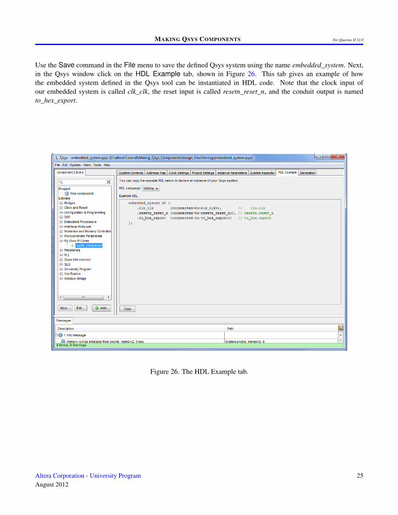
Use the Save command in the File menu to save the defined Qsys system using the name embedded_system. Next,in the Qsys window click on the HDL Example tab, shown in Figure 26. This tab gives an example of howthe embedded system defined in the Qsys tool can be instantiated in HDL code. Note that the clock input ofour embedded system is called clk_clk, the reset input is called resetn_reset_n, and the conduit output is namedto_hex_export.
Figure 26. The HDL Example tab.
Altera Corporation - University ProgramAugust 2012
25
MAKING QSYS COMPONENTS For Quartus II 12.0
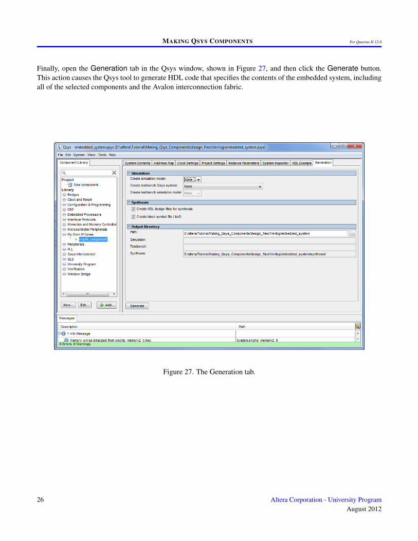
Finally, open the Generation tab in the Qsys window, shown in Figure 27, and then click the Generate button.This action causes the Qsys tool to generate HDL code that specifies the contents of the embedded system, includingall of the selected components and the Avalon interconnection fabric.
Figure 27. The Generation tab.
26 Altera Corporation - University ProgramAugust 2012
MAKING QSYS COMPONENTS For Quartus II 12.0
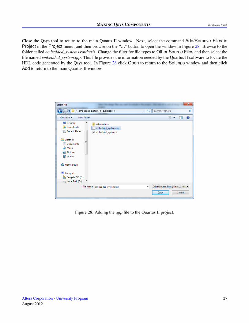
Close the Qsys tool to return to the main Quatus II window. Next, select the command Add/Remove Files inProject in the Project menu, and then browse on the “. . .” button to open the window in Figure 28. Browse to thefolder called embedded_system\synthesis. Change the filter for file types to Other Source Files and then select thefile named embedded_system.qip. This file provides the information needed by the Quartus II software to locate theHDL code generated by the Qsys tool. In Figure 28 click Open to return to the Settings window and then clickAdd to return to the main Quartus II window.
Figure 28. Adding the .qip file to the Quartus II project.
Altera Corporation - University ProgramAugust 2012
27
MAKING QSYS COMPONENTS For Quartus II 12.0
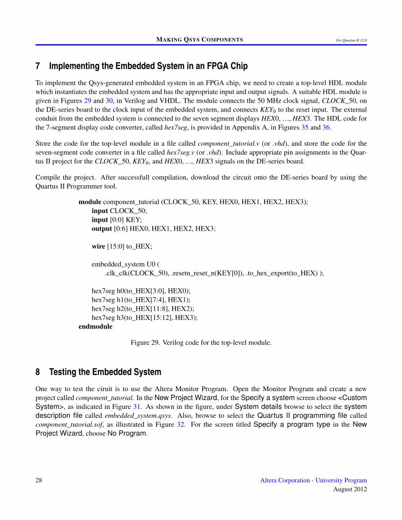
7 Implementing the Embedded System in an FPGA Chip
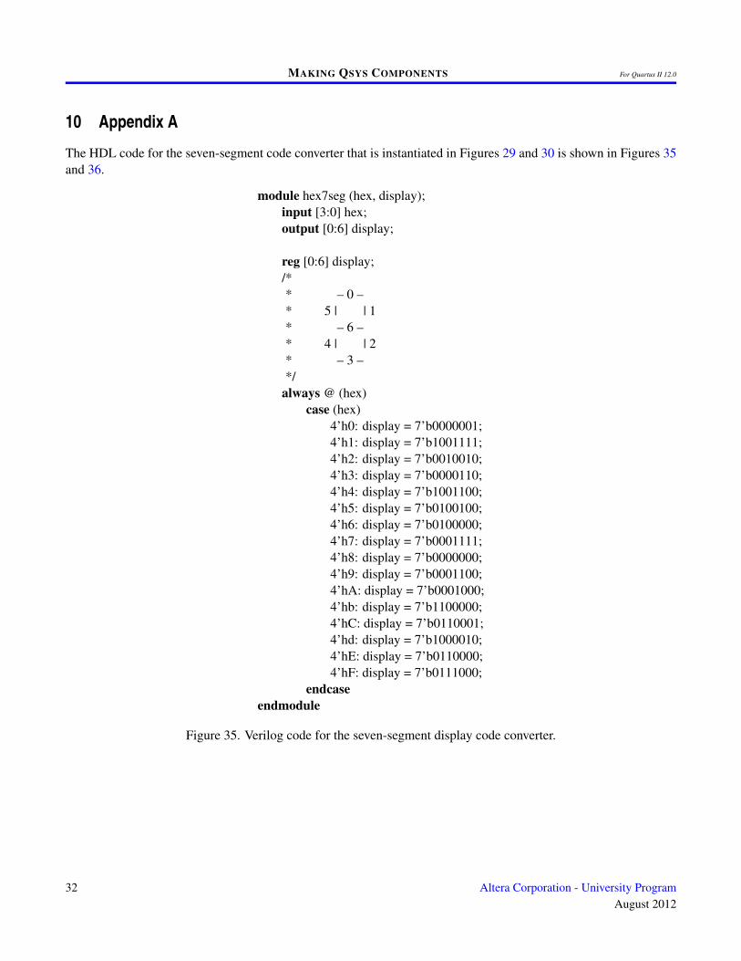
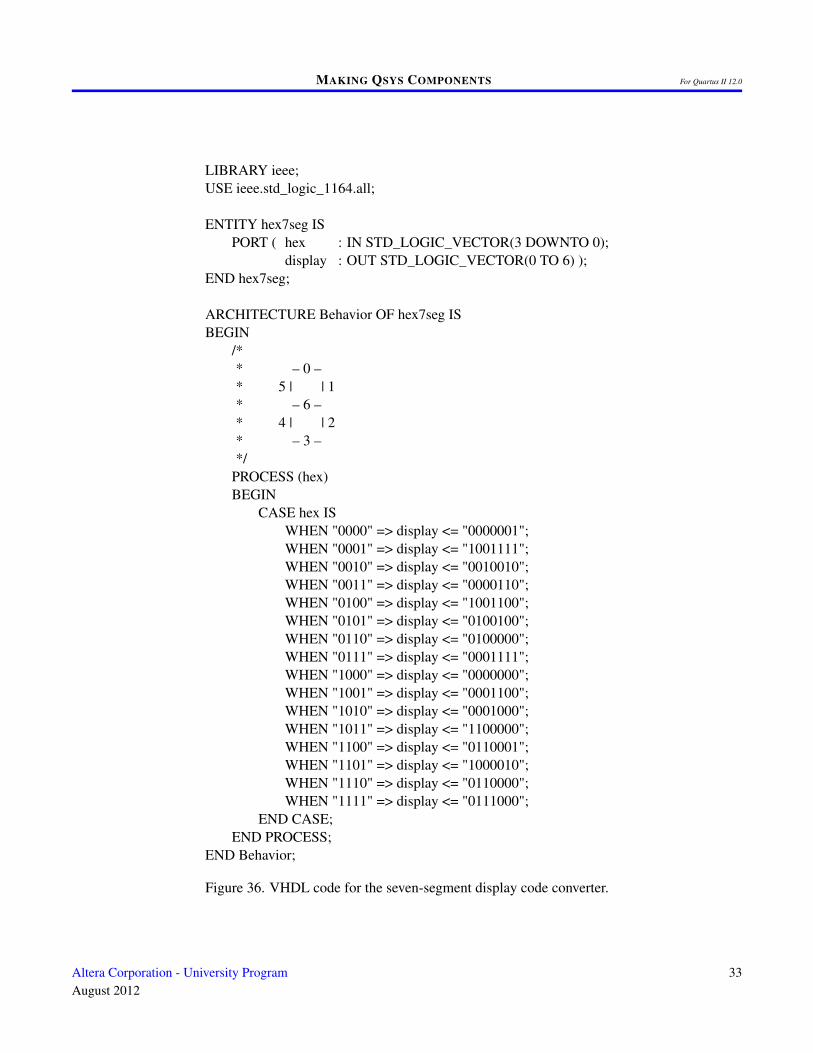
To implement the Qsys-generated embedded system in an FPGA chip, we need to create a top-level HDL modulewhich instantiates the embedded system and has the appropriate input and output signals. A suitable HDL module isgiven in Figures 29 and 30, in Verilog and VHDL. The module connects the 50 MHz clock signal, CLOCK_50, onthe DE-series board to the clock input of the embedded system, and connects KEY0 to the reset input. The externalconduit from the embedded system is connected to the seven segment displays HEX0, . . ., HEX3. The HDL code forthe 7-segment display code converter, called hex7seg, is provided in Appendix A, in Figures 35 and 36.
Store the code for the top-level module in a file called component_tutorial.v (or .vhd), and store the code for theseven-segment code converter in a file called hex7seg.v (or .vhd). Include appropriate pin assignments in the Quar-tus II project for the CLOCK_50, KEY0, and HEX0, . . ., HEX3 signals on the DE-series board.
Compile the project. After successfull compilation, download the circuit onto the DE-series board by using theQuartus II Programmer tool.
module component_tutorial (CLOCK_50, KEY, HEX0, HEX1, HEX2, HEX3);input CLOCK_50;input [0:0] KEY;output [0:6] HEX0, HEX1, HEX2, HEX3;
wire [15:0] to_HEX;
embedded_system U0 (.clk_clk(CLOCK_50), .resetn_reset_n(KEY[0]), .to_hex_export(to_HEX) );
hex7seg h0(to_HEX[3:0], HEX0);hex7seg h1(to_HEX[7:4], HEX1);hex7seg h2(to_HEX[11:8], HEX2);hex7seg h3(to_HEX[15:12], HEX3);
endmodule
Figure 29. Verilog code for the top-level module.
8 Testing the Embedded System
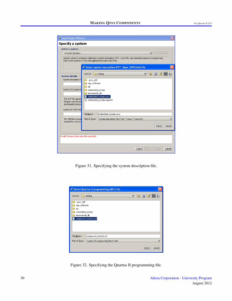
One way to test the ciruit is to use the Altera Monitor Program. Open the Monitor Program and create a newproject called component_tutorial. In the New Project Wizard, for the Specify a system screen choose <CustomSystem>, as indicated in Figure 31. As shown in the figure, under System details browse to select the systemdescription file called embedded_system.qsys. Also, browse to select the Quartus II programming file calledcomponent_tutorial.sof, as illustrated in Figure 32. For the screen titled Specify a program type in the NewProject Wizard, choose No Program.
28 Altera Corporation - University ProgramAugust 2012
MAKING QSYS COMPONENTS For Quartus II 12.0
LIBRARY ieee;USE ieee.std_logic_1164.all;
ENTITY component_tutorial ISPORT ( CLOCK_50 : IN STD_LOGIC;
KEY : IN STD_LOGIC_VECTOR(0 DOWNTO 0);HEX0 : OUT STD_LOGIC_VECTOR(0 TO 6);HEX1 : OUT STD_LOGIC_VECTOR(0 TO 6);HEX2 : OUT STD_LOGIC_VECTOR(0 TO 6);HEX3 : OUT STD_LOGIC_VECTOR(0 TO 6) );
END component_tutorial;
ARCHITECTURE Structure OF component_tutorial ISSIGNAL to_HEX : STD_LOGIC_VECTOR(15 DOWNTO 0);COMPONENT embedded_system IS
PORT ( clk_clk : IN STD_LOGIC;resetn_reset_n : IN STD_LOGIC;to_hex_export : OUT STD_LOGIC_VECTOR (15 DOWNTO 0) );
END COMPONENT embedded_system;
COMPONENT hex7seg ISPORT ( hex : IN STD_LOGIC_VECTOR(3 DOWNTO 0);
display : OUT STD_LOGIC_VECTOR(0 TO 6) );END COMPONENT hex7seg;
BEGINU0: embedded_system PORT MAP (
clk_clk => CLOCK_50,resetn_reset_n => KEY(0),to_hex_export => to_HEX );
h0: hex7seg PORT MAP (to_HEX(3 DOWNTO 0), HEX0);h1: hex7seg PORT MAP (to_HEX(7 DOWNTO 4), HEX1);h2: hex7seg PORT MAP (to_HEX(11 DOWNTO 8), HEX2);h3: hex7seg PORT MAP (to_HEX(15 DOWNTO 12), HEX3);
END Structure;
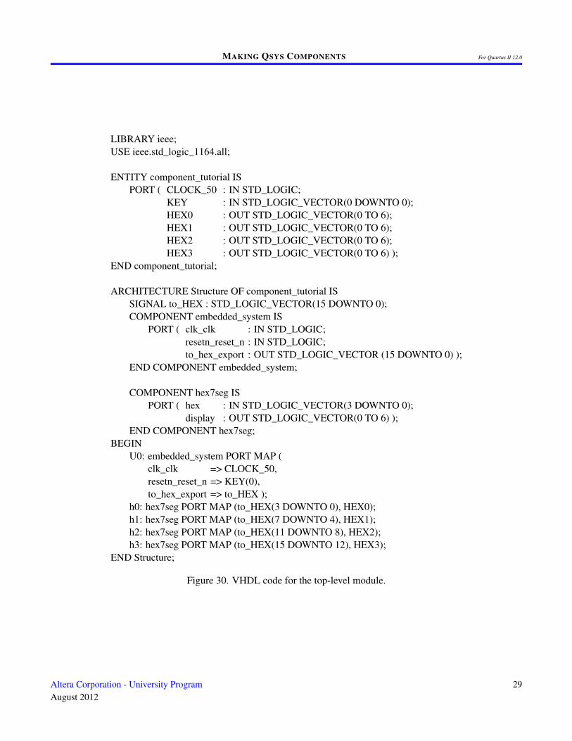
Figure 30. VHDL code for the top-level module.
Altera Corporation - University ProgramAugust 2012
29
MAKING QSYS COMPONENTS For Quartus II 12.0
Figure 31. Specifying the system description file.
Figure 32. Specifying the Quartus II programming file.
30 Altera Corporation - University ProgramAugust 2012
MAKING QSYS COMPONENTS For Quartus II 12.0
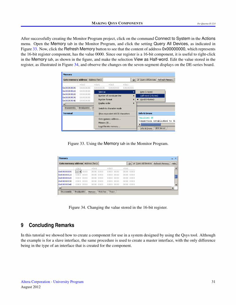
After successfully creating the Monitor Program project, click on the command Connect to System in the Actionsmenu. Open the Memory tab in the Monitor Program, and click the setting Query All Devices, as indicated inFigure 33. Now, click the Refresh Memory button to see that the content of address 0x00000000, which representsthe 16-bit register component, has the value 0000. Since our register is a 16-bit component, it is useful to right-clickin the Memory tab, as shown in the figure, and make the selection View as Half-word. Edit the value stored in theregister, as illustrated in Figure 34, and observe the changes on the seven-segment displays on the DE-series board.
Figure 33. Using the Memory tab in the Momitor Program.
Figure 34. Changing the value stored in the 16-bit register.
9 Concluding Remarks
In this tutorial we showed how to create a component for use in a system designed by using the Qsys tool. Althoughthe example is for a slave interface, the same procedure is used to create a master interface, with the only differencebeing in the type of an interface that is created for the component.
Altera Corporation - University ProgramAugust 2012
31
MAKING QSYS COMPONENTS For Quartus II 12.0
10 Appendix A
The HDL code for the seven-segment code converter that is instantiated in Figures 29 and 30 is shown in Figures 35and 36.
module hex7seg (hex, display);input [3:0] hex;output [0:6] display;
reg [0:6] display;/** – 0 –* 5 | | 1* – 6 –* 4 | | 2* – 3 –*/
always @ (hex)case (hex)
4’h0: display = 7’b0000001;4’h1: display = 7’b1001111;4’h2: display = 7’b0010010;4’h3: display = 7’b0000110;4’h4: display = 7’b1001100;4’h5: display = 7’b0100100;4’h6: display = 7’b0100000;4’h7: display = 7’b0001111;4’h8: display = 7’b0000000;4’h9: display = 7’b0001100;4’hA: display = 7’b0001000;4’hb: display = 7’b1100000;4’hC: display = 7’b0110001;4’hd: display = 7’b1000010;4’hE: display = 7’b0110000;4’hF: display = 7’b0111000;
endcaseendmodule
Figure 35. Verilog code for the seven-segment display code converter.
32 Altera Corporation - University ProgramAugust 2012
MAKING QSYS COMPONENTS For Quartus II 12.0
LIBRARY ieee;USE ieee.std_logic_1164.all;
ENTITY hex7seg ISPORT ( hex : IN STD_LOGIC_VECTOR(3 DOWNTO 0);
display : OUT STD_LOGIC_VECTOR(0 TO 6) );END hex7seg;
ARCHITECTURE Behavior OF hex7seg ISBEGIN
/** – 0 –* 5 | | 1* – 6 –* 4 | | 2* – 3 –*/
PROCESS (hex)BEGIN
CASE hex ISWHEN "0000" => display <= "0000001";WHEN "0001" => display <= "1001111";WHEN "0010" => display <= "0010010";WHEN "0011" => display <= "0000110";WHEN "0100" => display <= "1001100";WHEN "0101" => display <= "0100100";WHEN "0110" => display <= "0100000";WHEN "0111" => display <= "0001111";WHEN "1000" => display <= "0000000";WHEN "1001" => display <= "0001100";WHEN "1010" => display <= "0001000";WHEN "1011" => display <= "1100000";WHEN "1100" => display <= "0110001";WHEN "1101" => display <= "1000010";WHEN "1110" => display <= "0110000";WHEN "1111" => display <= "0111000";
END CASE;END PROCESS;
END Behavior;
Figure 36. VHDL code for the seven-segment display code converter.
Altera Corporation - University ProgramAugust 2012
33

MAKING QSYS COMPONENTS For Quartus II 12.0
Copyright © 2012 Altera Corporation. All rights reserved. Altera, The Programmable Solutions Company, thestylized Altera logo, specific device designations, and all other words and logos that are identified as trademarksand/or service marks are, unless noted otherwise, the trademarks and service marks of Altera Corporation in theU.S. and other countries. All other product or service names are the property of their respective holders. Alteraproducts are protected under numerous U.S. and foreign patents and pending applications, mask work rights, andcopyrights. Altera warrants performance of its semiconductor products to current specifications in accordance withAltera’s standard warranty, but reserves the right to make changes to any products and services at any time withoutnotice. Altera assumes no responsibility or liability arising out of the application or use of any information, product,or service described herein except as expressly agreed to in writing by Altera Corporation. Altera customers areadvised to obtain the latest version of device specifications before relying on any published information and beforeplacing orders for products or services.
This document is being provided on an “as-is” basis and as an accommodation and therefore all warranties, repre-sentations or guarantees of any kind (whether express, implied or statutory) including, without limitation, warrantiesof merchantability, non-infringement, or fitness for a particular purpose, are specifically disclaimed.
34 Altera Corporation - University ProgramAugust 2012