maharashtra state board of technical...
TRANSCRIPT

MAHARASHTRA STATE BOARD OF TECHNICAL EDUCATION (Autonomous)
(ISO/IEC - 27001 - 2005 Certified)
WINTER – 14 EXAMINATION Subject Code: 17431 Model Answer Subject Name: Microprocessor and
Programming
Page 1 of 40
Important Instructions to examiners:
1) The answers should be examined by key words and not as word-to-word as given in the model answer
scheme.
2) The model answer and the answer written by candidate may vary but the examiner may try to assess
the understanding level of the candidate.
3) The language errors such as grammatical, spelling errors should not be given more Importance (Not
applicable for subject English and Communication Skills).
4) While assessing figures, examiner may give credit for principal components indicated in the figure.
The figures drawn by candidate and model answer may vary. The examiner may give credit for any
equivalent figure drawn.
5) Credits may be given step wise for numerical problems. In some cases, the assumed constant values
may vary and there may be some difference in the candidate’s answers and model answer.
6) In case of some questions credit may be given by judgment on part of examiner of relevant answer
based on candidate’s understanding.
7) For programming language papers, credit may be given to any other program based on equivalent
concept.
Marks
1. (A) Attempt any SIX of the following: 12
(i) List any four salient features of 8085 microprocessor.
(Any four - ½ Marks each)
Ans: Silent features of 8085:
1. 16 address line so 216
=64 Kbytes of memory can be addressed.
2. Operating clock frequency is 3MHz and minimum clock frequency is 500 KHz.
3. On chip bus controller.
4. Provide 74 instructions with five addressing modes.
5. 8085 is 8 bit microprocessor.
6. Provides 5 level hardware interrupts and 8 software interrupts.
7. It can generate 8 bit I/O address so 28=256 input and 256 output ports can be accessed.
8. Requires a single +5 volt supply.

MAHARASHTRA STATE BOARD OF TECHNICAL EDUCATION (Autonomous)
(ISO/IEC - 27001 - 2005 Certified)
WINTER – 14 EXAMINATION Subject Code: 17431 Model Answer Subject Name: Microprocessor and
Programming
Page 2 of 40
(ii) State the names of segment registers in 8086 microprocessor.
(For each register - ½ Marks)
Ans: Segment registers in 8086 microprocessor:
o Code Segment register(CS)
o Data Segment register(DS)
o Stack Segment register(SS)
o Extra Segment register(ES)
(iii)Define addressing mode. List any two addressing modes of 8086 microprocessor.
(Definition – 1 Mark, List – 1 Mark (any two))
Ans: Addressing modes are the way of specifying an operand in an instruction
Immediate, Direct, Register, Register indirect, Indexed, Register relative, Based indexed, Relative
based indexed, Intersegment direct mode, Intersegment indirect mode, Intrasegment direct mode,
Intrasegment indirect mode.
(iv) Define flowchart & algorithm.
(For each definition – 1 Mark)
Ans: Algorithm: Algorithm is a task or sequence of operations performed by program.
Flowchart: Flow chart is a graphical representation of task or algorithm.
(v) List the names of flags in flag register of 8085 microprocessor.
(All Correct – 2 Marks)
Ans: Zero (Z), Carry (CY), Sign (S), Parity (P), and Auxiliary Carry (AC) flags.
(vi) Define pipelining. What is the size of instruction prefetch queue in 8086 microprocessor?
(Definition -1 Mark, prefetch queue size – 1 Mark)
Ans: In 8086, pipelining is the technique of overlapping instruction fetch and execution mechanism.
This will speed up the execution of program.
The size of instruction preftech queue in 8086 is 6 bytes.

MAHARASHTRA STATE BOARD OF TECHNICAL EDUCATION (Autonomous)
(ISO/IEC - 27001 - 2005 Certified)
WINTER – 14 EXAMINATION Subject Code: 17431 Model Answer Subject Name: Microprocessor and
Programming
Page 3 of 40
(vii) Write any two difference of FAR & NEAR procedures.
(Any two difference – 1 Mark each)
Ans:
NEAR procedure FAR procedure
A near call is a call to procedure which is
in same code segment
A far call is a call to procedure which is in
different segment
The contents of CS is not stored The contents of CS is also stored along with
offset.
In near call contents of SP is decremented
by 2 and contents of offset address IP is
stored
In Far call contents of SP are decremented by 2
and value of CS is loaded. Then SP is again
decremented by 2 and IP is loaded.
(viii) Write assembly language instructions of 8086 microprocessor to:
(a) Add 100 H to the contents of AX register.
(b) Rotate the contents of AX towards left by 2 bits.
(Each -1 Mark)
Ans: (a) Add 100H to contents of AX register
ADD AX, 100H
(b) Rotate the contents of AX towards left by 2 bits
MOV CL, 02H
RCL AX, CL
Or
MOV CL, 02H
ROL AX, CL
MAHARASHTRA STATE BOARD OF TECHNICAL EDUCATION (Autonomous)
(ISO/IEC - 27001 - 2005 Certified)
WINTER – 14 EXAMINATION Subject Code: 17431 Model Answer Subject Name: Microprocessor and
Programming
Page 4 of 40
(B) Attempt any TWO of the following: 8
(i) State the function of
(a) Editor
(b) Assembler
(Each - 2 Marks)
Ans: Editor
It is a program which helps to construct assembly language program with a file extension .asm, in
right format so that the assembler will translate it to machine language. It enables one to create,
edit, save, copy and make modification in source file.
Assembler
Assembler is a program that translates assembly language program to the correct binary code for
each instruction i.e. machine code and generate the file called as object file with extension .obj
(ii) List any four assembler directives. State the functions of any two assembler directives.
(Listing of any four - 2 Marks, Explanation of any two - 1 Mark each)
[Note: Students may also write directives from segment define directives and processor
directives]
Ans: Assembler directives are: 1) DB 2) DW 3) DQ 4) DT 5)? (Uninitialized value)
6) PTR 7) OFFSET 8) EQU 9) DUP 10) LABEL 11) ALIGN 12) EVEN 13) ORG
14) DOSSEG 15) STRUCT 16) DD
DB (Define Byte or Data Byte)
• This is used to define a byte type variable.
• The range of values : 0 – 255 for unsigned numbers
-128 to 127 for signed numbers
• This can be used to define a single byte or multiple bytes
DW (Define Word or Data Word)
• This is used to define a word (16-bit) type variable.
• The range of values : 0 – 65535 for unsigned numbers
-32768 to 32767 for signed numbers
• This can be used to define a single word or multiple words

MAHARASHTRA STATE BOARD OF TECHNICAL EDUCATION (Autonomous)
(ISO/IEC - 27001 - 2005 Certified)
WINTER – 14 EXAMINATION Subject Code: 17431 Model Answer Subject Name: Microprocessor and
Programming
Page 5 of 40
DD (Define Double Word or Data Double Word)
• This is used to define a double word (32-bit) type variable.
• The range of values : 0 – 232
- 1 bits for unsigned numbers
-232-1
to 232-1
- 1for signed numbers
• This can be used to define a single double word or multiple double word
EQU( Equate To)
• This is used to declare symbols to which some constant value is assigned
• The label assigned using this directive is used throught the program instead of the numeric
value.
• While assembling, whenever the assembler comes across the label, it substitutes the numeric
value for that label.
• Use of EQU is realised when the value of the symbol changes. The single modification in the
EQU directive will make the necessary changes at all places in the program.
EVEN
• The assembler while starting the assembling operation for any program, initialises a location
counter and goes on updating it, as the assembly progresses.
• It assigns addresses to program variables, constants and modules as per requirements
• EVEN directive can be used to reassign the addresses to these variables or constants with
Even address, if it was not so before.
• If location counter is already at the even address, no change is done by the assembler.
LABEL
• This enables the user to redefine the attribute of a data variable or instruction label.
ASSUME
• This informs the assembler the name of the logical segment which should be used for a
specified segment.
• The segment registers are pointed to the various logical segments using this directive.
SEGMENT
• This is used to indicate the beginning of the logical segment.
• The directives SEGMENT, ENDS are always enclosed in data, code, stack and extra
segments.

MAHARASHTRA STATE BOARD OF TECHNICAL EDUCATION (Autonomous)
(ISO/IEC - 27001 - 2005 Certified)
WINTER – 14 EXAMINATION Subject Code: 17431 Model Answer Subject Name: Microprocessor and
Programming
Page 6 of 40
• In some cases, the segments may be assigned a type like PUBLIC (used by other modules of
the program while linking) or GLOBAL (can be accessed by any other module).
ENDS :
• This directive informs the assembler the end of the segment
• The directives SEGMENT, ENDS are always enclosed in data, code, stack and extra
segments.
• Whatever are the contents of the segments, they should appear in the program before ENDS.
• Any statement appearing after ENDS will be neglected from the segment.
LENGTH
• This is used to refer to the length of a data array or a string.
OFFSET
• This operator first computes the 16 bit displacement of the particular label.
• Then it replaces the string “OFFSET LABEL by the computed displacement.
• This operator is used with Arrays, strings, labels and procedures to decide their default
segment offsets.
• It is usually used to load a offset of a variable into the register
SEG
• Used to decide the segment address of the label, variable, or procedure and substitutes the
segment base address in place of “SEG” label.
TYPE
• This directs the assembler to decide the data type of the specified label and replaces the TYPE
Label by the decided data type
• For Byte type variable, data type is 1
• For Word type variable, data type is 2
• For Double word type variable, data type is 4
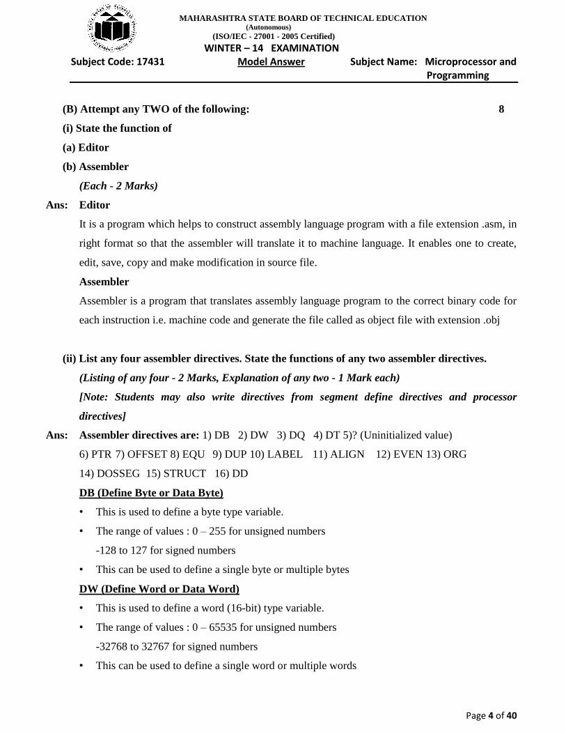
(iii)What do you mean by re-entrant procedures? Write any assembly language program with
re-entrant procedure.
(Re-entrant procedure – 1 Mark, Diagram with explanation - 3 Marks)
[Note: Any program relevant to the diagram may also be considered]
Ans: In some situation it may happen that Procedure 1is called from main program
MAHARASHTRA STATE BOARD OF TECHNICAL EDUCATION (Autonomous)
(ISO/IEC - 27001 - 2005 Certified)
WINTER – 14 EXAMINATION Subject Code: 17431 Model Answer Subject Name: Microprocessor and
Programming
Page 7 of 40
Procrdure2 is called from procedure1And procrdure1 is again called from procdure2.
In this situation program execution flow re enters in the procedure1. These types of procedures
are called re-entrant procedures.
OR
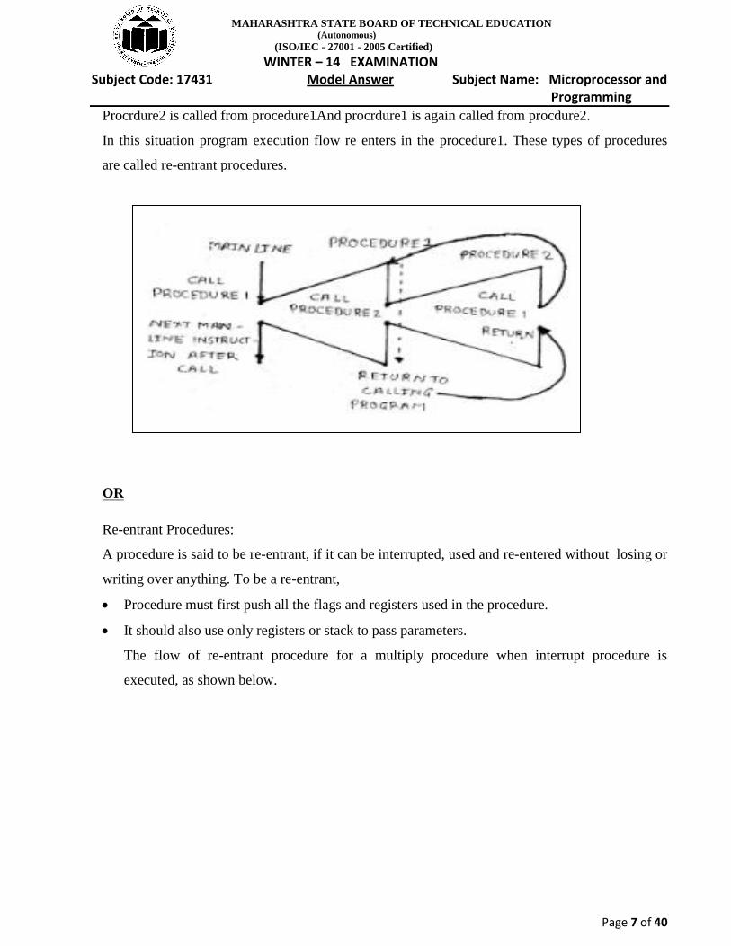
Re-entrant Procedures:
A procedure is said to be re-entrant, if it can be interrupted, used and re-entered without losing or
writing over anything. To be a re-entrant,
Procedure must first push all the flags and registers used in the procedure.
It should also use only registers or stack to pass parameters.
The flow of re-entrant procedure for a multiply procedure when interrupt procedure is
executed, as shown below.

MAHARASHTRA STATE BOARD OF TECHNICAL EDUCATION (Autonomous)
(ISO/IEC - 27001 - 2005 Certified)
WINTER – 14 EXAMINATION Subject Code: 17431 Model Answer Subject Name: Microprocessor and
Programming
Page 8 of 40
2. Attempt any FOUR of the following: 16
(a) List & explain the functions of all general purpose registers of 8085 microprocessor.
(List – 1 Mark, Explanation – 3 Marks)
Ans: 8085 microprocessor has the following registers.
1. One 8-bit accumulator (ACC) i.e. register A.
2. Six 8-bit general purpose registers. These are B, C, D, E, H and L.
3. Pair of two 8 bit register such as BC, DE and HL are used as 16 bit registers.
ACCUMULATOR
The accumulator A is an 8 bit register that is part of the arithmetic logic unit [ALU]. This register
is used to store 8 bit data and to perform arithmetic and logical operations. The result of the
operation is stored in the accumulator and identified as A.
B, C, D, E, H and L are used as 8-bit registers for storing data in a assembly language program.
BC, DE and HL are used as register pairs for 16 bit data manipulation.
Call
Multiply Interrupt
Here
Call
Multiply
Main Line Interrupt
Procedure
Return to
Interrupt
Multiply
procedure
Return to Calling program
MAHARASHTRA STATE BOARD OF TECHNICAL EDUCATION (Autonomous)
(ISO/IEC - 27001 - 2005 Certified)
WINTER – 14 EXAMINATION Subject Code: 17431 Model Answer Subject Name: Microprocessor and
Programming
Page 9 of 40
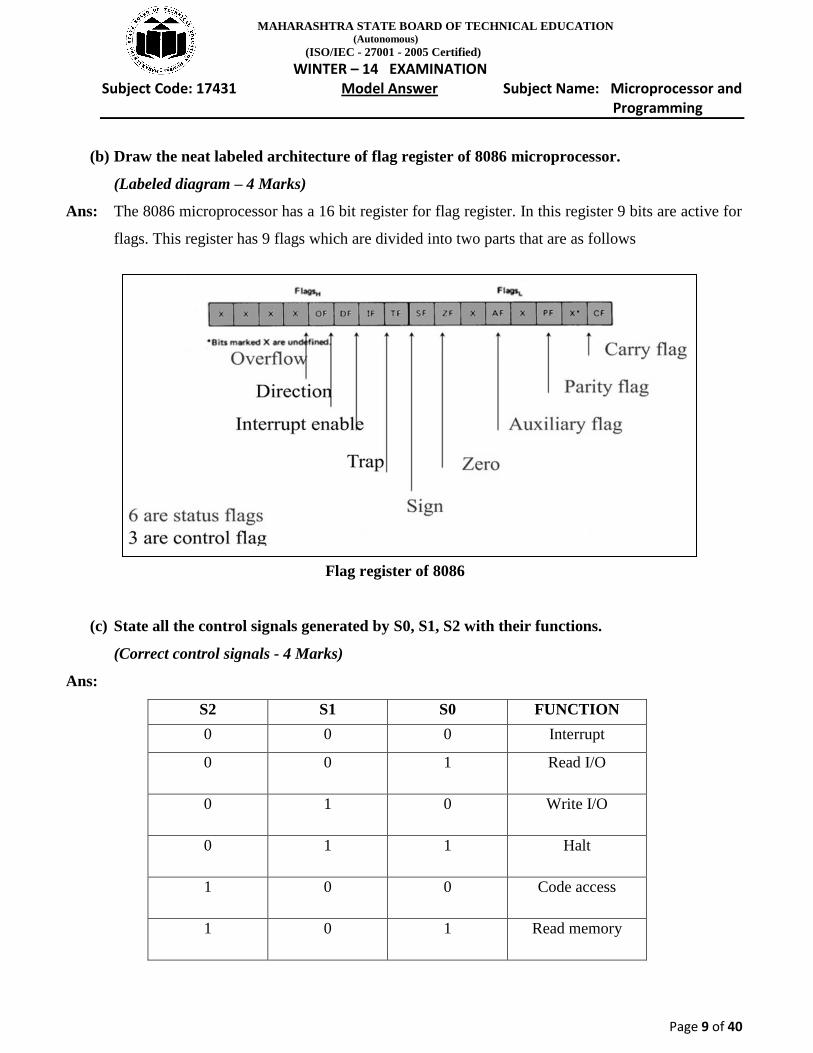
(b) Draw the neat labeled architecture of flag register of 8086 microprocessor.
(Labeled diagram – 4 Marks)
Ans: The 8086 microprocessor has a 16 bit register for flag register. In this register 9 bits are active for
flags. This register has 9 flags which are divided into two parts that are as follows
Flag register of 8086
(c) State all the control signals generated by S0, S1, S2 with their functions.
(Correct control signals - 4 Marks)
Ans:
S2 S1 S0 FUNCTION
0 0 0 Interrupt
acknowledge
0 0 1 Read I/O
0 1 0 Write I/O
0 1 1 Halt
1 0 0 Code access
1 0 1 Read memory

MAHARASHTRA STATE BOARD OF TECHNICAL EDUCATION (Autonomous)
(ISO/IEC - 27001 - 2005 Certified)
WINTER – 14 EXAMINATION Subject Code: 17431 Model Answer Subject Name: Microprocessor and
Programming
Page 10 of 40
1 1 0 Write memory
1 1 1 Inactive
(d) Compare 8085 microprocessor & 8086 microprocessor.( with respect to)
(i) No. of data lines
(ii) No. of address lines.
(iii)Frequency of operation
(iv) Registers
(Each comparison - 1 Mark)
Ans:
(e) What will be contents to AX register after execution of following lines of code:
MOV AL, 10
MOV DL, 20
MUL DL
(Correct answer – 4 Marks)
Ans:
AH AL
00 C8
OR
AX = 00C8H
8085 8086
No. of data lines 8 16
No. of address lines 16 20
Frequency of operation Clock speed 3MHZ Clock speed 5,8and 10 MHZ
Registers 8 Bit registers
OR
A, B, C, D, E, H and
L
16 Bit registers
OR
AX, BX, CX, DX or others
may be considered

MAHARASHTRA STATE BOARD OF TECHNICAL EDUCATION (Autonomous)
(ISO/IEC - 27001 - 2005 Certified)
WINTER – 14 EXAMINATION Subject Code: 17431 Model Answer Subject Name: Microprocessor and
Programming
Page 11 of 40
f) Describe the physical memory address generation process in 8086 microprocessor. If, CS =
69FAH & IP = 834CH, calculate the physical address generated.
(Description – 2 Marks, Calculation - 2 Marks)
Ans: The 8086 addresses a segmented memory. The complete physical address which is 20-bits long is
generated using segment and offset registers each of the size 16-bit.The content of a segment
register also called as segment address, and content of an offset register also called as offset
address. To get total physical address, put the lower nibble 0H to segment address and add offset
address. The figure shows formation of 20-bit physical address.
Physical address formation
0110 1001 1111 1010 0000
1000 0011 0100 1100
0111 0010 0010 1110 1100
7 2 2 E C
= 722EC H
+

MAHARASHTRA STATE BOARD OF TECHNICAL EDUCATION (Autonomous)
(ISO/IEC - 27001 - 2005 Certified)
WINTER – 14 EXAMINATION Subject Code: 17431 Model Answer Subject Name: Microprocessor and
Programming
Page 12 of 40
3. Attempt any FOUR of the following: 16
a) Write any two arithmetic instructions & logical instructions with their functions. Give the
syntax with one example each.
(For each instruction, syntax -1 Mark, Example – 1 Mark)
Ans:
Any two arithmetic instructions from the following or any other
1. ADD Destination, Source
Example:
ADD AL, 74H
ADD DX, AX
ADD AX, [BX]
2. ADC Destination, Source
Example:
ADC AL, 74H
ADC DX, AX
ADC AX, [BX]
3. SUB Destination, Source
Example:
SUB AL, 74H
SUB DX, AX
SUB AX, [BX]
4. SBB Destination, Source
Example:
SBB AL, 74H
SBB DX, AX
SBB AX, [BX]

MAHARASHTRA STATE BOARD OF TECHNICAL EDUCATION (Autonomous)
(ISO/IEC - 27001 - 2005 Certified)
WINTER – 14 EXAMINATION Subject Code: 17431 Model Answer Subject Name: Microprocessor and
Programming
Page 13 of 40
5. INC Destination
Example:
INC AX
INC BL
6. DEC Destination
Example:
DEC AX
DEC CL
7. MUL (Unsigned multiplication)
Syntax: MUL source
Examples:
1. MUL BL ; Multiply AL by BL & the result in AX
2. MUL CX ; Multiply AX by CX & the result in DX,AX
3. MUL Byte PTR [SI] ; AX AL * [SI]
8. IMUL (Signed multiplication)
Syntax: IMUL source
Example:
1. IMUL BL ; Multiply AL by BL & the result in AX
2. IMUL CX ; Multiply AX by CX & the result in DX,AX
3. IMUL Byte PTR [SI] ; AX AL * [SI]
9. DIV (Unsigned Division)
Syntax: DIV source
Examples:
1. DIV BL ; Divide word in AX by byte in BL, Quotient is stored in AL,
remainder in AH.
2. DIV CX ; Divide double word in DX:AX by word in CX, Quotient in AX,
Remainder in DX.

MAHARASHTRA STATE BOARD OF TECHNICAL EDUCATION (Autonomous)
(ISO/IEC - 27001 - 2005 Certified)
WINTER – 14 EXAMINATION Subject Code: 17431 Model Answer Subject Name: Microprocessor and
Programming
Page 14 of 40
3. DIV [BX] ; Divide word in AX by byte in memory location pointer by BX.
Any two logical instructions from the following or any other
AND (Logical AND)
Syntax: AND destination, source
Examples:
1. AND BH,CL ;AND byte in CL with Byte in BH, result in BH.
2. AND BX,00FFH ;AND word in BX with immediate data 00ffH
3. AND [5000H], DX ;AND word in DX with a word in memory with offset 5000 in DS.
OR (Logical OR)
Syntax: OR destination, source
Examples:
1. OR BH,CL ;OR byte in CL with Byte in BH, result in BH.
2. OR BX,00FFH ;OR word in BX with immediate data 00ffH
3. OR [5000H], DX ; OR word in DX with a word in memory with offset 5000 in DS.
XOR (Logical XOR)
Syntax: XOR destination, source
Examples:
1. XOR BH,CL ;XOR byte in CL with Byte in BH, result in BH.
2. XOR BX,00FFH ;XOR word in BX with immediate data 00ffH
3. XOR [5000H], DX ; XOR word in DX with a word in memory with offset 5000 in DS.
NOT (Logical Invert)
Syntax: NOT destination
Examples:
1. NOT BH ;Complement byte in BH, result in BH.
2. NOT BX ; Complement word in BX, result in BX.
3. NOT BYTE PTR [5000H] ; Complement byte in memory with offset 5000 in DS.

MAHARASHTRA STATE BOARD OF TECHNICAL EDUCATION (Autonomous)
(ISO/IEC - 27001 - 2005 Certified)
WINTER – 14 EXAMINATION Subject Code: 17431 Model Answer Subject Name: Microprocessor and
Programming
Page 15 of 40
b) State the functions of following pins of 8086 microprocessor:
(i) ALE
(ii) DT /
(iii) M /
(iv) HOLD
(Per pin description – 1 Mark)
Ans:
(i) ALE: - This output signal is used to indicate availability of valid address on address/data lines
and is connected to latch enable input of latches .This signal is active high and never tristate.
(ii) DT/ :- This output line is used to decide the direction of data flow through the transceivers
(bidirectional buffer). When the processor sends the data, this signal is high and when the
processor is receiving data, this signal is low.
(iii) M/ :- This is status line logically equivalent to in maximum mode .When it is low, it
indicates the CPU is having an I/O operation, and when it is high, it indicates that CPU is
having memory operation. This line becomes active in Previous T4 of current cycle. It is tri-
stated during local bus hold acknowledgment.
(iv) HOLD:-This line is used to indicate to 8086 that another master is requesting the bus access.

MAHARASHTRA STATE BOARD OF TECHNICAL EDUCATION (Autonomous)
(ISO/IEC - 27001 - 2005 Certified)
WINTER – 14 EXAMINATION Subject Code: 17431 Model Answer Subject Name: Microprocessor and
Programming
Page 16 of 40
c) Draw the interfacing of 8284 clock generator with 8086 microprocessor. List and explain
interfacing signals.
(Diagram – 2 Marks, List – 1 Mark, function -1 Mark)
Ans:
1. Generate system clock: The Clock logic results in three different frequencies required for the
system. These outputs are CLOCK, OSC and PCLK.
2. Generate READY signal: The Ready logic has a READY output which is connected to the
processor. When this is low, wait states are added in the bus cycle.
3. Generate RESET signal: The Reset logic generates a RESET input for the microprocessor. When
this signal is High, processor performs reset sequence.
MAHARASHTRA STATE BOARD OF TECHNICAL EDUCATION (Autonomous)
(ISO/IEC - 27001 - 2005 Certified)
WINTER – 14 EXAMINATION Subject Code: 17431 Model Answer Subject Name: Microprocessor and
Programming
Page 17 of 40
d) List & explain any four string operation instructions with their functions & syntax.
(Each instruction operation -1 Mark, only listing - 1 Mark will be considered)
Ans: 1] REP: REP is a prefix which is written before one of the string instructions. It will cause during
length counter CX to be decremented and the string instruction to be repeated until CX becomes
0.
Two more prefix.
REPE/REPZ: Repeat if Equal /Repeat if Zero.
It will cause string instructions to be repeated as long as the compared bytes or words are equal
and CX≠0.
REPNE/REPNZ: Repeat if not equal/Repeat if not zero.
It repeats the strings instructions as long as compared bytes or words are not equal and CX≠0.
Example: REP MOVSB
2] MOVS/ MOVSB/ MOVSW - Move String byte or word.
Syntax
MOVS destination, source
MOVSB destination, source
MOVSW destination, source
Operation: ES:[DI]<----- DS:[SI]
It copies a byte or word a location in data segment to a location in extra segment. The offset of
source is pointed by SI and offset of destination is pointed by DI.CX register contain counter and
direction flag (DE) will be set or reset to auto increment or auto decrement pointers after one
move. Example
LEA SI, Source
LEA DI, destination
CLD
MOV CX, 04H
REP MOVSB

MAHARASHTRA STATE BOARD OF TECHNICAL EDUCATION (Autonomous)
(ISO/IEC - 27001 - 2005 Certified)
WINTER – 14 EXAMINATION Subject Code: 17431 Model Answer Subject Name: Microprocessor and
Programming
Page 18 of 40
3] CMPS /CMPSB/CMPSW: Compare string byte or Words.
Syntax
CMPS destination, source
CMPSB destination, source
CMPSW destination, source
Operation: Flags affected < ----- DS:[SI]- ES:[DI]
It compares a byte or word in one string with a byte or word in another string. SI holds the offset
of source and DI holds offset of destination strings. CS contains counter and DF=0 or 1 to auto
increment or auto decrement pointer after comparing one byte/word.
Example
LEA SI, Source
LEA DI, destination
CLD
MOV CX, 100
REPE CMPSB
4] SCAS/SCASB/SCASW: Scan a string byte or word.
Syntax
SCAS/SCASB/SCASW
Operation: Flags affected < ----- AL/AX-ES: [DI]
It compares a byte or word in AL/AX with a byte /word pointed by ES: DI. The string to be
scanned must be in the extra segment and pointed by DI. CX contains counter and DF may be 0
or 1.
When the match is found in the string execution stops and ZF=1 otherwise ZF=0 .
Example
LEA DI, destination
MOV Al, 0DH
MOV CX, 80H
CLD
REPNE SCASB
MAHARASHTRA STATE BOARD OF TECHNICAL EDUCATION (Autonomous)
(ISO/IEC - 27001 - 2005 Certified)
WINTER – 14 EXAMINATION Subject Code: 17431 Model Answer Subject Name: Microprocessor and
Programming
Page 19 of 40
5] LODS/LODSB/LODSW: Load String byte into AL or Load String word into AX.
Syntax: LODS/LODSB/LODSW
Operation: AL/AX < ----- DS: [SI]
IT copies a byte or word from string pointed by SI in data segment into AL or AX.CX may
contain the counter and DF may be either 0 or 1
Example
LEA SI, destination
CLD
LODSB
6] STOS/STOSB/STOSW (Store Byte or Word in AL/AX)
Syntax STOS/STOSB/STOSW
Operation: ES:[DI] < ----- AL/AX
It copies a byte or word from AL or AX to a memory location pointed by DI in extra segment CX
may contain the counter and DF may either set or reset.
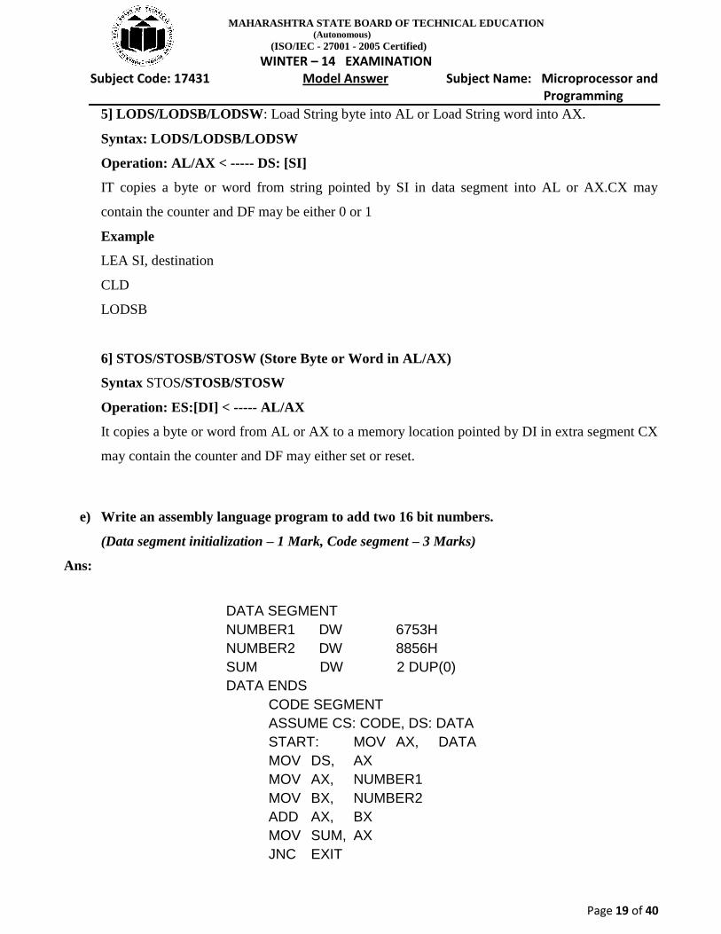
e) Write an assembly language program to add two 16 bit numbers.
(Data segment initialization – 1 Mark, Code segment – 3 Marks)
Ans:
DATA SEGMENT
NUMBER1 DW 6753H
NUMBER2 DW 8856H
SUM DW 2 DUP(0)
DATA ENDS
CODE SEGMENT
ASSUME CS: CODE, DS: DATA
START: MOV AX, DATA
MOV DS, AX
MOV AX, NUMBER1
MOV BX, NUMBER2
ADD AX, BX
MOV SUM, AX
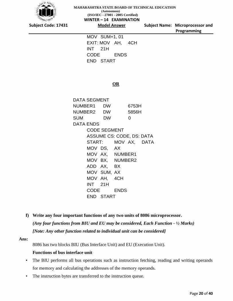
JNC EXIT
MAHARASHTRA STATE BOARD OF TECHNICAL EDUCATION (Autonomous)
(ISO/IEC - 27001 - 2005 Certified)
WINTER – 14 EXAMINATION Subject Code: 17431 Model Answer Subject Name: Microprocessor and
Programming
Page 20 of 40
OR
f) Write any four important functions of any two units of 8086 microprocessor.
(Any four functions from BIU and EU may be considered, Each Function - ½ Marks)
[Note: Any other function related to individual unit can be considered]
Ans:
8086 has two blocks BIU (Bus Interface Unit) and EU (Execution Unit).
Functions of bus interface unit
• The BIU performs all bus operations such as instruction fetching, reading and writing operands
for memory and calculating the addresses of the memory operands.
• The instruction bytes are transferred to the instruction queue.
MOV SUM+1, 01
EXIT: MOV AH, 4CH
INT 21H
CODE ENDS
END START
DATA SEGMENT
NUMBER1 DW 6753H
NUMBER2 DW 5856H
SUM DW 0
DATA ENDS
CODE SEGMENT
ASSUME CS: CODE, DS: DATA
START: MOV AX, DATA
MOV DS, AX
MOV AX, NUMBER1
MOV BX, NUMBER2
ADD AX, BX
MOV SUM, AX
MOV AH, 4CH
INT 21H
CODE ENDS
END START

MAHARASHTRA STATE BOARD OF TECHNICAL EDUCATION (Autonomous)
(ISO/IEC - 27001 - 2005 Certified)
WINTER – 14 EXAMINATION Subject Code: 17431 Model Answer Subject Name: Microprocessor and
Programming
Page 21 of 40
• BIU contains Instruction queue, Segment registers, Instruction pointer, and Address adder.
• BIU controls the address, data and control buses.
• It provides a full 16 bit bidirectional data bus and 20 bit address bus.
• The bus interface unit is responsible for performing all external bus operations.
• Instruction fetch, Instruction queuing, Operand fetch and storage, Address relocation and Bus
control are the operations performed by BIU
• The BIU uses a mechanism known as an instruction stream queue to implement a pipeline
architecture.
Functions of Execution Unit
• EU executes instructions from the instruction system byte queue.
• Both units operate asynchronously to give the 8086 an overlapping instruction fetch and
execution mechanism which is called as Pipelining. This results in efficient use of the system bus
and system performance.
• EU contains Control circuitry, Instruction decoder, ALU, Pointer and Index register, Flag register.
• The Execution unit is responsible for decoding and executing all instructions.
• The EU extracts instructions from the top of the queue in the BIU, decodes them, generates
operands if necessary, passes them to the BIU and requests it to perform the read or write bys
cycles to memory or I/O and perform the operation specified by the instruction on the operands.
• During the execution of the instruction, the EU tests the status and control flags and updates them
based on the results of executing the instruction.
• If the queue is empty, the EU waits for the next instruction byte to be fetched and shifted to top of
the queue.
• When the EU executes a branch or jump instruction, it transfers control to a location
corresponding to another set of sequential instructions.
• Whenever this happens, the BIU automatically resets the queue and then begins to fetch
instructions from this new location to refill the queue.
• EU has a 16 bit ALU, which can perform arithmetic and logical operations on 8 bit as well as 16
bit data.

MAHARASHTRA STATE BOARD OF TECHNICAL EDUCATION (Autonomous)
(ISO/IEC - 27001 - 2005 Certified)
WINTER – 14 EXAMINATION Subject Code: 17431 Model Answer Subject Name: Microprocessor and
Programming
Page 22 of 40
OR
The Instruction Queue:
To implement any instruction first it is to be fetched, then decoded and then executed. The
fetching of an instruction involves its address to be sent out to the system memory and then the
memory sending back the instruction.
While the EU is busy decoding or executing certain instructions which do not need the buses, the
BIU fetches next six instruction bytes and stores them in a first-in-first-out (FIFO) register set
called queue.
The processor doesn't have to wait for the next instruction to be fetched as it is already made
available in the queue registers. Thus, the speed of operation is enhanced.
This prefetching of next instruction while another instruction is still being executed is known
as pipelining.
General-purpose Registers:
There are eight 8-bit general-purpose registers: AL, AH, BL, BH, CL, CH, DL andDH. These can
be used for temporary storage of 8-bit data. They can also be used for storage for 16-bit data
words as groups: AXregister (AH and AL), BX register (BH and BL),CX register (CH and CL)
and DX register (DH and DL).
Their exact functions will be encountered latter.
Flags:
The 16-bit flag register of 8086 contains 9 active flags (six conditional & 3 control) , other 7 flags
are undefined.
Conditional Flags: indicate certain condition that arises during the execution. They are controlled
by the processor.
Control Flags: control certain operations of the processor. They are deliberately set/reset by the
user.
Other Registers:
The Segment Registers- SS, DS, CS and ES, the pointer and index registers -BP, SP, SI and DI.
and the Instruction Pointer (IP) will be discussed along with 8086 memory.
ALU:- ALU is used to perform arithmetic and logical operations

MAHARASHTRA STATE BOARD OF TECHNICAL EDUCATION (Autonomous)
(ISO/IEC - 27001 - 2005 Certified)
WINTER – 14 EXAMINATION Subject Code: 17431 Model Answer Subject Name: Microprocessor and
Programming
Page 23 of 40
Address generator: - This unit is used to generate 20 bit physical address by adding 16 bit
logical address displacement with base address
Instruction Decoder:- This unit is used convert or decode the instructions and provides signals to
various units in the EU.
4. Attempt any FOUR of the following: 16
(a) Identify the addressing modes of following instructions:
(i) MUL AL, BL
(ii) MOV AX, BX
(iii) MOV BX, [S1]
(iv) MOV DX, 0040H
(Each addressing mode - 1 Mark each)
Ans:
i) MUL AL,BL:- Register addressing mode
ii) MOV AX ,BX:- Register addressing mode
iii) MOV BX,[SI]:-Indexed addressing mode
iv) MOV DX,0040H:-Immediate addressing mode
b) Explain the following instructions of 8086 microprocessor with their syntax:
(i) STRCMP
(ii) ADD
(Each – 2 Marks)
Ans: (i) STRCMP:-
(There is no instructions such as STRCMP. Instead, CMPS instruction may be considered as
given below
CMPS/CMPSB/CMPSW
Syntax : CMPS destination, source
CMPSB

MAHARASHTRA STATE BOARD OF TECHNICAL EDUCATION (Autonomous)
(ISO/IEC - 27001 - 2005 Certified)
WINTER – 14 EXAMINATION Subject Code: 17431 Model Answer Subject Name: Microprocessor and
Programming
Page 24 of 40
CMPSW
• The CMPS instruction is used to compare a byte or a word in the source string with a byte or a
word in the destination string.
• The source must be in the data segment and the destination in the extra segment.
• The offset of the source byte or a word must be placed in SI register, which is represented as
DS:SI and the offset of the destination byte or a word must be placed in DI register, which is
represented as ES:DI
• On the execution of the instruction, SI and DI are automatically adjusted by one to the next
element of the source and destination.
• If the Direction Flag is reset (DF = 0), the registers SI and DI will be incremented by one for the
byte comparison and incremented by two for the word comparison.
• If the Direction Flag is set (DF = 1), the registers SI and DI will be decremented by one for the
byte comparison and decremented by two for the word comparison
• The DS:SI and ES:DI register must be loaded prior to the execution of the CMPS instruction.
• CMPSB and CMPSW are the implicit instructions to move a byte or word string .
• The instruction CMPSB is used to compare a byte from the source with destination and the
instruction CMPSW is used to compare a word in the source with destination.
• In multiple byte or word comparison, the count must be loaded in CX register which functions as
a counter.
• All conditional flags are affected
OR
Operation Performed :--
If dest string > source string then CF =0, ZF = 0, SF = 0
If dest string < source string then CF =1, ZF = 0, SF = 1
If dest string = source string then CF =0, ZF = 1, SF = 0
If a byte comparison,
For DF =0, SI SI +1 & DI DI +1
For DF =1, SI SI -1 & DI DI – 1
If a word comparison,
For DF =0, SI SI +2 & DI DI +2
For DF =1, SI SI -2 & DI DI - 2

MAHARASHTRA STATE BOARD OF TECHNICAL EDUCATION (Autonomous)
(ISO/IEC - 27001 - 2005 Certified)
WINTER – 14 EXAMINATION Subject Code: 17431 Model Answer Subject Name: Microprocessor and
Programming
Page 25 of 40
(iii) ADD:-This instruction is used to add immediate data to contain of register or to add content
of one register (or memory location )to another register (or memory location )
Syntax:-
ADD destination, source
Destination may be register or memory location and source may be data, memory location’s
or registers.
c) Write an assembly language program to find smallest number from array of 5 elements.
(Correct program – 4 Marks)
Ans: .model small
.data
array1 db 12h,31h,02h,45h,65h
small db 0
.code
mov ax,@data
mov ds,ax
mov cx,5
mov si,offset array1
mov al,[si]
dec cx
Up : inc si
cmp al,[si]
jc next
mov al,[si]
next:
loop up
mov small ,al
ends
end

MAHARASHTRA STATE BOARD OF TECHNICAL EDUCATION (Autonomous)
(ISO/IEC - 27001 - 2005 Certified)
WINTER – 14 EXAMINATION Subject Code: 17431 Model Answer Subject Name: Microprocessor and
Programming
Page 26 of 40
d) Write an assembly language program to find the length of a string using 8086.
(Correct program - 4 Marks)
Ans: .model small
.data
a1 db "sdk$"
.code
mov ax,@data
mov ds,ax
mov cl,00h
lea si,a1
x:
mov al,[si]
cmp al,'$'
je y
inc cl
inc si
jmp x
y:
mov ah,4ch
int 21h
ends
end
OR
Data Segment
STRG DB 'GOOD MORNING$'
LEN DB ?
DATA ENDS

MAHARASHTRA STATE BOARD OF TECHNICAL EDUCATION (Autonomous)
(ISO/IEC - 27001 - 2005 Certified)
WINTER – 14 EXAMINATION Subject Code: 17431 Model Answer Subject Name: Microprocessor and
Programming
Page 27 of 40
e) Write an assembly language program to add two BCD numbers using 8086.
(Correct program - 4 Marks)
[Note: Program without carry can also be considered]
Ans: ASSUME CS: CODE , DS:DATA
DATA SEGMENT
OP1 EQU 92H
OP2 EQU 52H
RESULT DB 02 DUP(00)
DATA ENDS
CODE SEGMENT
CODE SEGMENT
START: ASSUME CS: CODE,
DS : DATA
MOV DX, DATA
MOV DS,DX
LEA SI, STRG
MOV CL,00H
MOV AL,'$'
NEXT: CMP AL,[SI]
JZ EXIT
ADD CL,01H
INC SI
JMP NEXT
EXIT: MOV LEN,CL
MOV AH,4CH
INT 21H
CODE ENDS

MAHARASHTRA STATE BOARD OF TECHNICAL EDUCATION (Autonomous)
(ISO/IEC - 27001 - 2005 Certified)
WINTER – 14 EXAMINATION Subject Code: 17431 Model Answer Subject Name: Microprocessor and
Programming
Page 28 of 40
START:
MOV AX,DATA
MOV DS,AX
MOV BL,OP1
XOR AL,AL
MOV AL,OP2
ADD AL,BL
DAA
MOV RESULT ,AL
JNC MSBO
INC [RESULT+1]
MSBO: MOV AH,4CH
INT 21H
CODE ENDS
END START
f) Define Macro. Write assembler directives used in Macros. Explain.
(Definition - 1 Mark, List – 1 Mark, Explanation - 2 Marks)
Ans: Definition: - Macro is sequence of instruction(s) which gets repeated in program specified with
specific name & repletion of this sequence is replaced by this name while coding small sequences
of codes of the same pattern repeated frequently at different places which perform the same
operation on the different data of the same data type are called MACRO. Macro is also called as
an Open subroutine. When called, the codes written within macro are executed automatically.
Macros should be used when it has few program statements. This simplifies the programming
process.
Macro directives:-
i) MACRO
ii) ENDM

MAHARASHTRA STATE BOARD OF TECHNICAL EDUCATION (Autonomous)
(ISO/IEC - 27001 - 2005 Certified)
WINTER – 14 EXAMINATION Subject Code: 17431 Model Answer Subject Name: Microprocessor and
Programming
Page 29 of 40
i) MACRO:- This macro directive is used to specify beginning of a macro definition( coding of
macro )
ii) ENDM:- ENDM:- This directive is used to specify end of macro definition
5. Attempt any FOUR of the following: 16
(a) Write an assembly language program to add the series of 5 numbers.
(Correct program - 4 Marks)
Ans:
Label Mnemonics
data segment
Array
1000h,2000h,1500h,1200h,3500h
sum_lower dw 0000h
sum_upper dw 0000h
data ends
code segment
Start:
assume cs: code, ds:data
mov ax, data
mov ds, ax
mov cl, 05h
mov ax,0000h
mov si,offset array
up: mov ax, [si]
Add sum_lower,ax
Jnc next
Inc sum_upper
Next: Inc si
Inc si
Loop up
mov ax, 4c00h
int 21h
code ends
End start

MAHARASHTRA STATE BOARD OF TECHNICAL EDUCATION (Autonomous)
(ISO/IEC - 27001 - 2005 Certified)
WINTER – 14 EXAMINATION Subject Code: 17431 Model Answer Subject Name: Microprocessor and
Programming
Page 30 of 40
(b) What will be the contents of AL, BL, AX, DX registers, after the execution of all 4 lines:
MOV AL, 03H
MOV BL, 03H
SUB AL,BL
MUL AL, 08H
Also write which flags will be affected?
(Register contents- 2 Marks, Flag – 2 Marks)
[Note: If the student corrects MUL instructions and writes the output, marks can be given]
Ans: The above program segment gives an error at MUL instructions hence it gives no output.
After correction;
MUL instruction will be MUL AL
The contains of AL=00
MOV AL, 03H ; AL=03H
MOV BL, 03H ; BL=03H
SUB AL,BL; AL=00H
MUL AL; AL=00H
CF = 0, ZF = 1, SF= 0, OF= 0, PF=1, AF=0
(c) Write an assembly language program to add only odd numbers in the list of following
elements:
6, 5, 21, 3, 8, 9.
(Correct program - 4 Marks)
Ans: DATA SEGMENT
ARRAY DB 06H,05H,21H,03H,08H,09H
SUM DB 0H
DATA ENDS
CODE SEGMENT
ASSUME DS:DATA, CS:CODE
START: MOV AX,DATA
MOV DS,AX
MAHARASHTRA STATE BOARD OF TECHNICAL EDUCATION (Autonomous)
(ISO/IEC - 27001 - 2005 Certified)
WINTER – 14 EXAMINATION Subject Code: 17431 Model Answer Subject Name: Microprocessor and
Programming
Page 31 of 40
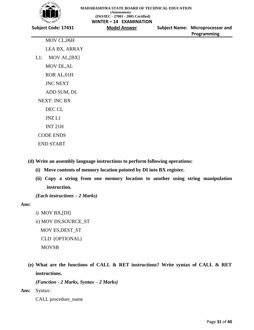
MOV CL,06H
LEA BX, ARRAY
L1: MOV AL,[BX]
MOV DL,AL
ROR AL,01H
JNC NEXT
ADD SUM, DL
NEXT: INC BX
DEC CL
JNZ L1
INT 21H
CODE ENDS
END START
(d) Write an assembly language instructions to perform following operations:
(i) Move contents of memory location pointed by DI into BX register.
(ii) Copy a string from one memory location to another using string manipulation
instruction.
(Each instructions – 2 Marks)
Ans:
i) MOV BX,[DI]
ii) MOV DS,SOURCE_ST
MOV ES,DEST_ST
CLD (OPTIONAL)
MOVSB
(e) What are the functions of CALL & RET instructions? Write syntax of CALL & RET
instructions.
(Function - 2 Marks, Syntax – 2 Marks)
Ans: Syntax:
CALL procedure_name
MAHARASHTRA STATE BOARD OF TECHNICAL EDUCATION (Autonomous)
(ISO/IEC - 27001 - 2005 Certified)
WINTER – 14 EXAMINATION Subject Code: 17431 Model Answer Subject Name: Microprocessor and
Programming
Page 32 of 40
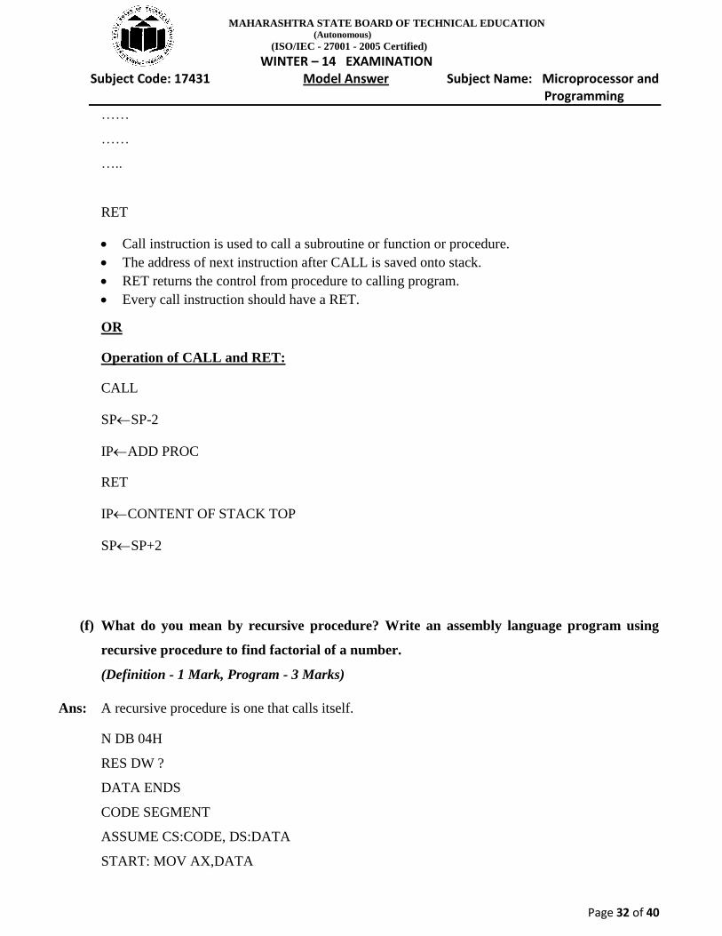
……
……
…..
RET
Call instruction is used to call a subroutine or function or procedure.
The address of next instruction after CALL is saved onto stack.
RET returns the control from procedure to calling program.
Every call instruction should have a RET.
OR
Operation of CALL and RET:
CALL
SPSP-2
IPADD PROC
RET
IPCONTENT OF STACK TOP
SPSP+2
(f) What do you mean by recursive procedure? Write an assembly language program using
recursive procedure to find factorial of a number.
(Definition - 1 Mark, Program - 3 Marks)
Ans: A recursive procedure is one that calls itself.
N DB 04H
RES DW ?
DATA ENDS
CODE SEGMENT
ASSUME CS:CODE, DS:DATA
START: MOV AX,DATA

MAHARASHTRA STATE BOARD OF TECHNICAL EDUCATION (Autonomous)
(ISO/IEC - 27001 - 2005 Certified)
WINTER – 14 EXAMINATION Subject Code: 17431 Model Answer Subject Name: Microprocessor and
Programming
Page 33 of 40
MOV DS,AX
MOV AL,N
MOV AH,00H
CALL FACT
INT 3
FACT PROC
CMP AX,01 ;IF N=1, FACT=1 ELSE FACT=N*FACT(N-1)
JZ EXIT
PUSH AX
DEC AX ;N-1
CALL FACT ;FACT(N-1)
POP AX
MUL RES ;N*FACT(N-1)
MOV RES,AX ;RES=FACTORIAL
RET
EXIT:
MOV RES,01
RET
FACT ENDP
CODE ENDS
END START

MAHARASHTRA STATE BOARD OF TECHNICAL EDUCATION (Autonomous)
(ISO/IEC - 27001 - 2005 Certified)
WINTER – 14 EXAMINATION Subject Code: 17431 Model Answer Subject Name: Microprocessor and
Programming
Page 34 of 40
6. Attempt any TWO of the following: 16
(a) With the neat diagram, describe the maximum mode operation of 8086.
List & describe function of signals of maximum mode of 8086.
(Diagram – 4 Marks, List – 2 Marks, Description - 2 Marks)
Ans:
AD15-AD0:-These pins acts as multiplexed address and data bus of the microprocessor.
Whenever the ALE pin is high these pins carry the address, when the ALE pin is low it carry the
data.
A19/S6-A16/S3:- These pins are multiplexed to provide the address signals A19-A16 and the
status bits S6-S3. When ALE=1 these pins carry the address and when ALE=0, they carry the
status lines.
S4 S3 Segment
Accessed
0 0 Extra Segment
0 1 Stack Segment
1 0 Code Segment
1 1 Data Segment
MAHARASHTRA STATE BOARD OF TECHNICAL EDUCATION (Autonomous)
(ISO/IEC - 27001 - 2005 Certified)
WINTER – 14 EXAMINATION Subject Code: 17431 Model Answer Subject Name: Microprocessor and
Programming
Page 35 of 40
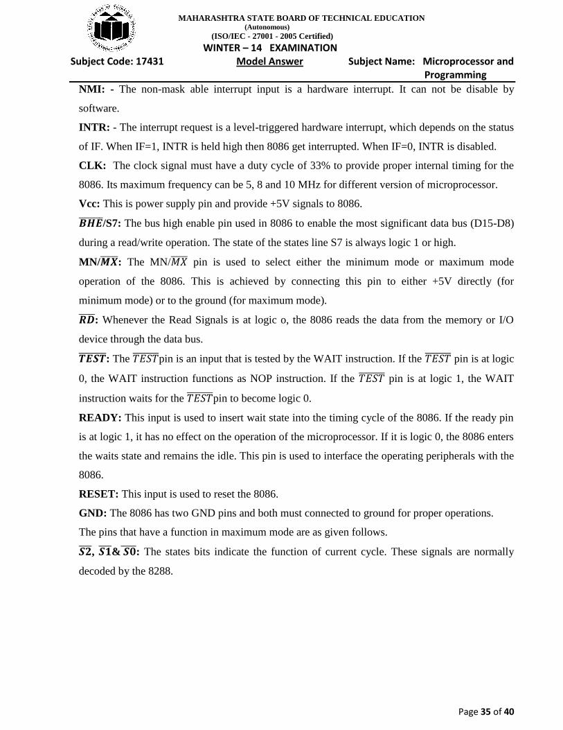
NMI: - The non-mask able interrupt input is a hardware interrupt. It can not be disable by
software.
INTR: - The interrupt request is a level-triggered hardware interrupt, which depends on the status
of IF. When IF=1, INTR is held high then 8086 get interrupted. When IF=0, INTR is disabled.
CLK: The clock signal must have a duty cycle of 33% to provide proper internal timing for the
8086. Its maximum frequency can be 5, 8 and 10 MHz for different version of microprocessor.
Vcc: This is power supply pin and provide +5V signals to 8086.
/S7: The bus high enable pin used in 8086 to enable the most significant data bus (D15-D8)
during a read/write operation. The state of the states line S7 is always logic 1 or high.
MN/ : The MN/ pin is used to select either the minimum mode or maximum mode
operation of the 8086. This is achieved by connecting this pin to either +5V directly (for
minimum mode) or to the ground (for maximum mode).
: Whenever the Read Signals is at logic o, the 8086 reads the data from the memory or I/O
device through the data bus.
: The pin is an input that is tested by the WAIT instruction. If the pin is at logic
0, the WAIT instruction functions as NOP instruction. If the pin is at logic 1, the WAIT
instruction waits for the pin to become logic 0.
READY: This input is used to insert wait state into the timing cycle of the 8086. If the ready pin
is at logic 1, it has no effect on the operation of the microprocessor. If it is logic 0, the 8086 enters
the waits state and remains the idle. This pin is used to interface the operating peripherals with the
8086.
RESET: This input is used to reset the 8086.
GND: The 8086 has two GND pins and both must connected to ground for proper operations.
The pins that have a function in maximum mode are as given follows.
, & : The states bits indicate the function of current cycle. These signals are normally
decoded by the 8288.

MAHARASHTRA STATE BOARD OF TECHNICAL EDUCATION (Autonomous)
(ISO/IEC - 27001 - 2005 Certified)
WINTER – 14 EXAMINATION Subject Code: 17431 Model Answer Subject Name: Microprocessor and
Programming
Page 36 of 40
S2 S1 S0 Function
0 0 0 INTR
0 0 1 I/O Read
0 1 0 I/O Write
0 1 1 Halt
1 0 0 Op-code Fetch
1 0 1 Memory Read
1 1 0 Memory Write
1 1 1 Passive
: The output is used to look peripheral off the system. This pin is activated by using
prefix on any instruction.
/ & / :- The request/grant pins request DMA during the maximum mode operations
of 8086. These lines are bi-directional and are used to request and grant a DMA operation.
QS1 & QS0:- The queue states bit show the states of the internal instruction queue in 8086.
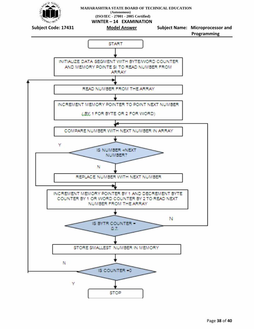
(b) Write an assembly language program to sort the array of 5 elements in ascending order.
Also draw the flowchart for the same.
(Program - 4 Marks, Flow chart – 4 Marks)
Ans: DATA SEGMENT
NUM DB 06H,09H,22H,02H,07H
RESULT DB ?
DATA ENDS
CODE SEGMENT
ASSUME CS:CODE,DS:DATA
START: MOV AX,DATA
MOV DS,AX
MOV CL,05H

MAHARASHTRA STATE BOARD OF TECHNICAL EDUCATION (Autonomous)
(ISO/IEC - 27001 - 2005 Certified)
WINTER – 14 EXAMINATION Subject Code: 17431 Model Answer Subject Name: Microprocessor and
Programming
Page 37 of 40
LOOP1: LEA BX,NUM
MOV CH,04H
LOOP2: MOV AL,[BX]
INC BX
CMP AL,[BX]
JC DOWN
MOV DL,[BX]
MOV [BX],AL
DEC BX
MOV [BX],DL
INC BX
DOWN: DEC CH
JNZ LOOP2
DEC DL
JNZ LOOP1
INT 3
CODE ENDS
END START
MAHARASHTRA STATE BOARD OF TECHNICAL EDUCATION (Autonomous)
(ISO/IEC - 27001 - 2005 Certified)
WINTER – 14 EXAMINATION Subject Code: 17431 Model Answer Subject Name: Microprocessor and
Programming
Page 38 of 40

MAHARASHTRA STATE BOARD OF TECHNICAL EDUCATION (Autonomous)
(ISO/IEC - 27001 - 2005 Certified)
WINTER – 14 EXAMINATION Subject Code: 17431 Model Answer Subject Name: Microprocessor and
Programming
Page 39 of 40
(c) Write an assembly language program to multiply two 8 bits numbers using NEAR
procedure. Also draw the flowchart for the same.
(Program -4 Marks, Flow chart – 4 Marks)
Ans: DATA SEGMENT
NUM1 DB 53H
NUM2 DB 33H
RES DW ?
DATA ENDS
CODE SEGMENT
ASSUME DS:DATA, CS:CODE
START: MOV AX,DATA
MOV DS,AX
CALL MULT
INT 3H
MULT PROC
MOV AL, NUM1
MUL NUM2
MOV RES, AX
RET
MULT ENDP
CODE ENDS
END START

MAHARASHTRA STATE BOARD OF TECHNICAL EDUCATION (Autonomous)
(ISO/IEC - 27001 - 2005 Certified)
WINTER – 14 EXAMINATION Subject Code: 17431 Model Answer Subject Name: Microprocessor and
Programming
Page 40 of 40
Flowchart:
Start
Initialize address of DS
Call Procedure Procedure
Stop Multiply data using MUL
instruction
Initialize Registers with data
Stored the result
Return to main program