magneto–optical kerr effect microscopy …etheses.whiterose.ac.uk/4543/1/thesis...
TRANSCRIPT
Magneto–Optical Kerr Effect
Microscopy Investigation on
Permalloy Nanostructures
Zulzawawi Bin Haji Hujan
A thesis submitted for the degree of
MSc by research
University of York
Department of Physics
January 2013

1
Abstract
This thesis focuses on the investigation of magnetic domains in ultrasmall permalloy
(Ni80Fe20) structures down to nanometre size. Magnetic domains and domain walls in
nano objects are often observed using a very high resolution and high power
microscope such as magnetic soft x-ray microscope, magnetic force microscopy
imaging and photoemission electron microscopy. A reason for this is because the
Kerr signal in nanostructures is very weak. However the results from this thesis
demonstrate that magnetic domains in permalloy magnetic nanostructures can still
be observed with very good contrast using a Magneto-optical Kerr effect (MOKE)
microscope. The constructed Kerr microscope is a home-build wide field microscope
and is able to produce magnetic domains image of permalloy nanowire as small as
245 nm, although the resolution limit of the microscope is 505 nm. For the first time,
a magnetic domain in nanowire with width of 245 nm is observed using a wide-field
microscope. The combination of hysteresis loops and magnetic domains
observations for studying a magnetic sample provides a three-dimensional
understanding of the magnetic characteristic of the sample. This is crucial in
investigating nano samples as the theoretical arguments with the experimental
results are always constrained by the experimental part. Three kinds of
nanostructure sample were observed using the Kerr microscope; a cross nanowire,
zigzag nanowire and a nanowire with notch and a nucleation pad at one end. It was
found that a cross nanowire can form magnetic domains upon reversal and the
junction forms a magnetisation vortex. Findings from zigzag nanowire demonstrate a
complex, multiple magnetic domains formation upon magnetisation reversal. A weak
domain wall pinning effect was observed in the nanowire, causing a multiple
domains formation in the nanowire upon reversal. It can be confirmed that this effect
was caused by the high coercivity of the nucleation pad. For the nanowire with notch,
it was demonstrated that the coercivities were different at negative and positive field.
But for such case, there is a relationship observed between the percentage notch
depth and the coercivity at the junction.

2
Table of Contents
Acknowledgement................................................................................................................................4
Declaration............................................................................................................................................5
1. Introduction and Background theory ......................................................................................... 6
1.1 Introduction ............................................................................................................................ 6
1.2 Background theory ............................................................................................................... 8
1.2.1 Ferromagnetism............................................................................................................ 8
1.2.2 Weiss theory ................................................................................................................. 8
1.2.3 Exchange interaction theory ..................................................................................... 10
1.2.4 Hysteresis loop ........................................................................................................... 11
1.2.5 Magnetic domains and domain walls ...................................................................... 12
1.2.6 Shape anisotropy ....................................................................................................... 14
1.3 Different energy densities in ferromagnetic material .................................................... 15
1.3.1 Magnetocrystalline anisotropy .................................................................................. 15
1.3.2 Exchange energy ....................................................................................................... 17
1.3.3 Magnetoelastic energy .............................................................................................. 18
1.3.4 Magnetostatic energy ................................................................................................ 18
1.3.5 Zeeman energy ........................................................................................................... 19
1.4 Domain walls ....................................................................................................................... 19
1.4.1 Bloch wall ..................................................................................................................... 19
1.4.2 Néel wall ...................................................................................................................... 21
1.5 Magnetic domains and domain walls in permalloy nanowire ...................................... 23
1.6 Domain walls pinning behaviour in nanowire with notch .............................................. 27
2. Experimental Method ................................................................................................................. 28
2.1 Introduction .......................................................................................................................... 28
2.2 Other methods .................................................................................................................... 29
2.3 Magneto-optical Kerr effect ............................................................................................... 29
2.4 Geometries of Kerr effect .................................................................................................. 31
2.5 Wide-field Kerr microscope set up ................................................................................... 37
2.6 Optics ................................................................................................................................... 39
2.7 Sources of noise ................................................................................................................. 40
2.8 Light source ......................................................................................................................... 41
2.9 Kohler illumination and field diaphragm .......................................................................... 42

3
2.10 Aperture diaphragm ........................................................................................................... 45
2.11 Compensator ....................................................................................................................... 47
2.12 Lateral Resolution and magnification of objective lens ................................................ 48
2.13 Camera ................................................................................................................................ 50
2.14 Electromagnet ..................................................................................................................... 51
2.15 Programming ....................................................................................................................... 52
2.15.1 Taking sets of images in loop. .................................................................................. 53
2.15.2 Magneto-optical magnetometry ................................................................................ 54
2.15.3 Analyse sets of images and digital contrast enhancement .................................. 57
2.16 Sample preparation ............................................................................................................ 59
2.17 OOMMF Simulation ........................................................................................................... 60
3. Results and discussions ............................................................................................................ 64
3.1 Focused MOKE magnetometer result ............................................................................. 64
3.2 Result from nickel iron (Ni80Fe20) thin film ...................................................................... 65
3.3 Nanowires results ............................................................................................................... 66
3.4 Cross-wire sample ............................................................................................................. 67
3.5 Zigzag nanowire ................................................................................................................. 71
3.6 Nanowires with asymmetric notch and nucleation pad ................................................ 77
3.6.1 Group one .................................................................................................................... 79
3.6.2 Discussion for group one .......................................................................................... 83
3.6.3 Group two .................................................................................................................... 84
3.6.4 Discussion ................................................................................................................... 96
4. Summary and conclusions ........................................................................................................ 99
4.1 Further work ...................................................................................................................... 101
5. Appendices ................................................................................................................................ 102
5.1 Appendix 1: Programme to extract the hysteresis loop for the magneto-optical
magnetometry ............................................................................................................................... 102
5.2 Appendix 2: Programme for taking a sets of pictures with known magnetic field for
each picture ................................................................................................................................... 102
5.3 Appendix 3: Programme to analyse the sets of images and to do digital contrast
enhancement ................................................................................................................................ 103
6. Bibliography............................................................................................................................... 104

4
Acknowledgement
I would like to take this opportunity to thank all the people who have helped and
support me all the way through my Master. First of all I would like to thank my
supervisor, Dr Jing Wu who supervised my work and giving me ideas. Also, thanks
to Xuefeng Hu who was making all the samples for my experiment. I would like to
thank Tuyuen Cheng for his support and help throughout my Master. I would also
like to express my gratitude to Prof Yongbing Xu for his advice on writing my thesis. I
would like to extend my gratitude to my parents whom always giving me supports
throughout my master. Last but not least, I would like to thank Siti Raheemah for
being supportive and taking care of me at all time throughout my Master.

5
Declaration
I hereby declare that the work contained in this thesis is my own and has not been
submitted for examination for any other degree at any University. All collaborators
works have been acknowledged in this thesis. All the nickel iron (Ni80Fe20) samples
mentioned in the thesis were fabricated by Xuefeng Hu. And the simulation result for
one sample mentioned in the result chapter was done also by Xuefeng Hu. Both the
fabrications and simulation were done in the University of York.

6
1. Introduction and Background theory
1.1 Introduction
Study of magnetism has been of interest for centuries, the first known magnetic
material was magnetite (Fe3O4) and its earliest description was recorded around
2500 years ago. But at that time, the development and study of magnetism was very
limited not until 1920 when the first understanding of the relationship between
electricity and magnetism was introduced by Hans Christian Oersted. He discovered
that an electric current produces magnetic field. Along with the first electromagnet
built in 1825, the study of magnetic materials increased dramatically because of the
available high power magnetic fields produced using electromagnet [1].
In 1898, Valdemar Poulsens’s invented the telegraphone to record voice [2]. This
was the beginning of the magnetic storage phenomenon. Further in nineteen fifties
the first commercial hard disk drive was introduced by IBM with only 4.4 megabyte of
storage density. The small storage density of the hard disk drive continued to
increase significantly until in the year 2000 where the increase is in the order of five
magnitude as shown in Figure 1.1. Recently, the areal density of the HDD is more
than 250 Gb/in2, and densities as high as 520 Gb/in2 have been demonstrated in the
laboratory [3]. The change of the areal density of magnetic storage can be seen on
Figure 1.1 showing how the high demand for magnetic storage had an impact on the
immense development in magnetic storage. The introduction of perpendicular
recording in 2005 has largely increased the areal density of HDD. But further
increase of the areal density is hindered due to the superparamagnetic effect.
Superparamagnetic effect refers to the fluctuation of magnetisation due to thermal
agitation when the magnetic grain size (bit size) is too small.

7
Figure 1.1: Graph showing the increasing areal density of HDD [4].
With the magnetic recording as the key technology to support the information
technology for our daily life, a lot of efforts were made to find other methods of
information storage. One of the proposed methods was the use of nano magnetic
objects as a high density magnetic storage device [5] and other well-known example
is the magnetic domain-wall racetrack memory [6]. Though, the possible use of nano
magnetic objects is not only limited to magnetic storage. For instance, the
ferromagnetic nanowires are said to have the potential for future magnetic and
spintronic devices such as magnetic diode [7] and magnetic logic gate [8]. Because
of the possibility of nanowires as the future spintronic devices, interest in the study of
magnetic nanowires has enormously increased. A lot of studies and researches have
been conducted to understand the magnetic properties of nanostructures materials.
However, understanding of the magnetic properties of nanostructures objects is still
a challenging theoretical issue as well as experimental issue.

8
1.2 Background theory
1.2.1 Ferromagnetism
Iron, cobalt, nickel, and permalloy such as nickel iron (Ni80Fe20) are examples of
ferromagnetic materials. In 1907, Pierre Weiss published his hypothesis on
ferromagnetic materials [9], which gives an in-depth understanding of ferromagnetic
materials behaviour for the first time. The hypothesis explains that magnetic
moments in ferromagnetic materials interact with each other where every single one
of them tries to align the others in its own direction. This hypothesis leads to the
Curie Weiss law:
Equation 1.1
where is the magnetic susceptibility of the material, C is the curie constant, T is the
absolute temperature and is the Curie-Weiss constant, Ferromagnetic material
remains its magnetisation even after removing the applied magnetic field. Weiss
theory deduced that the existence of magnetic domains in ferromagnetic materials
explains their demagnetisation state but Weiss did not explain the origin of magnetic
domains. Therefore Heisenberg came up with a theory by using quantum
mechanical approach to describe these domains. He explained that the origins of
these domains are the result of exchange interactions between magnetic moments in
ferromagnetic materials. Both theories will be explained in the next section below.
1.2.2 Weiss theory
The most important advancement in understanding ferromagnetic was the
introduction of ferromagnetic domain concept introduced by Weiss in two papers [9,
10]. These two papers were developed based on the earlier work of Ampere, Weber
and Ewing which proposed the existence of magnetic domains in ferromagnetic
material. It also explains that magnetic moments are in order even in demagnetized
state and these magnetic domains are consistently reorienting during magnetisation
process by external magnetic field. As explained before that these magnetic domains
will stay in the aligned order until it reaches the Curie temperature where the
9
ferromagnetic properties will change to paramagnetic. To explain this change, Weiss
use the Langevin model of paramagnetism where it uses the Curie law of
paramagnetic susceptibility to calculate the change in ferromagnetic to paramagnetic
properties.
Weiss theory was a pioneer in explaining the spontaneous magnetisation in
ferromagnetic materials. In the Weiss theory, it proposes the mean (molecular) field,
Hm to be proportional to the spontaneous magnetisation, Ms of the magnetic domain
and gives [11]:
Equation 1.2
where is the mean field constant. The Weiss molecular field is the effect in the
interatomic interaction causing the neighbouring magnetic moments to align parallel
to each other in order to reach the lowest energy state. This shows that the
interaction between magnetic moments in atoms causing the molecular field which is
an internal field that is strong enough to magnetise the material without the presence
of external applied magnetic field. Therefore the effective magnetic field acting
within a magnetic domain is:
Equation 1.3
where is the external magnetic field. Using Weiss theory, it generates the value of
molecular field in iron to be of the order 107 Oe [12]. But it only takes a field of
the order 1 Oe to rearrange the domains in iron and 103 Oe and to remove them.
Above the Curie temperature, the Curie law becomes:
Equation 1.4
Using gives:
Equation 1.5
where is the Curie temperature but when the temperature is above , is
used as shown in Equation 1.1. This explains the paramagnetic properties of
ferromagnetic material at temperature above Curie temperature.
10
Even though Weiss theory seems to be invalid, it is actually logical in describing the
approximation of a coupling force between spin and can be used to describe basic
understanding of ferromagnetism. Furthermore, there are general agreement
between the theoretical results of Weiss theory and experimental results for sample
like Fe, Ni [13] and Co. It is concluded that Weiss field theory is too simple as it did
not include the thermal fluctuations and the possible fluctuations between spins.
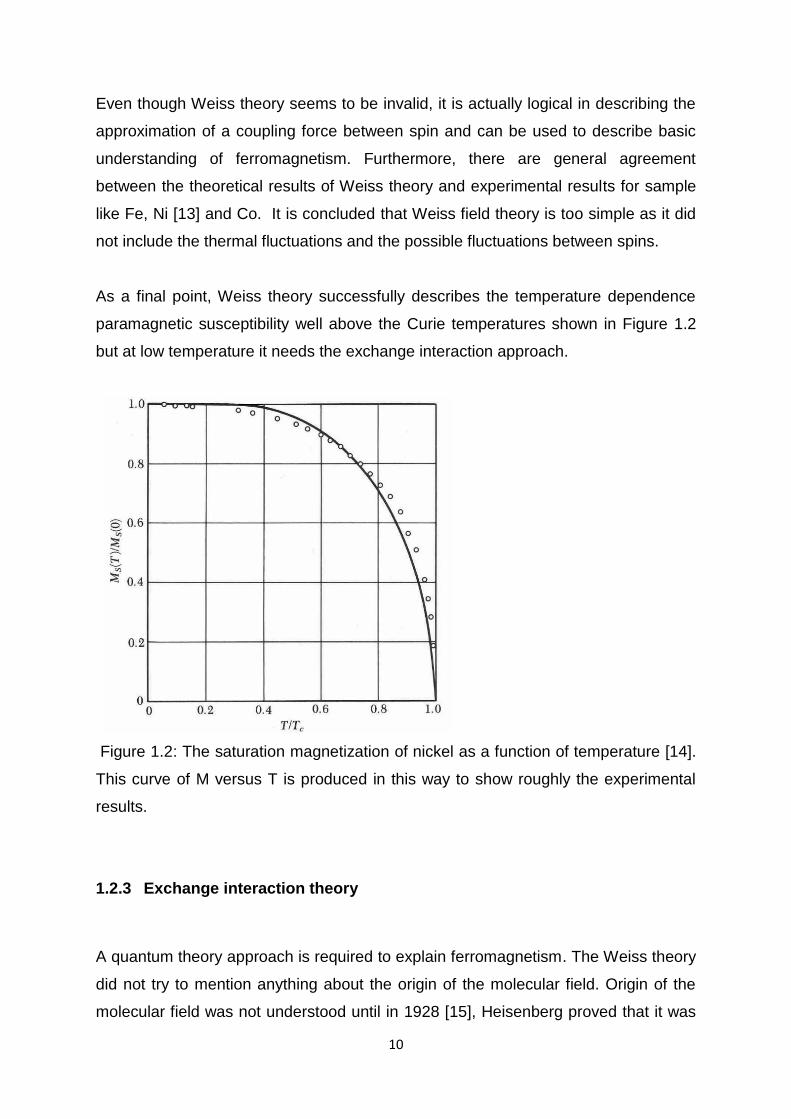
As a final point, Weiss theory successfully describes the temperature dependence
paramagnetic susceptibility well above the Curie temperatures shown in Figure 1.2
but at low temperature it needs the exchange interaction approach.
Figure 1.2: The saturation magnetization of nickel as a function of temperature [14].
This curve of M versus T is produced in this way to show roughly the experimental
results.
1.2.3 Exchange interaction theory
A quantum theory approach is required to explain ferromagnetism. The Weiss theory
did not try to mention anything about the origin of the molecular field. Origin of the
molecular field was not understood until in 1928 [15], Heisenberg proved that it was

11
caused by the quantum mechanical exchange interaction in the atoms. Heisenberg
Theory is based on the Pauli exclusion principle. The Heisenberg exchange
interaction based on effective interaction between the two neighbouring electron
spins is written as:
Equation 1.6
where and are the spin angular momentum vectors of the two electrons and
refers to the exchange integral between the two electrons. If the exchange integral is
positive ( >0), it will give ferromagnetism where parallel arrangement is favoured as
it gives the lowest energy. When is negative and large, it will give antiferromagnetic
or ferromagnetic where the spins alignment will be anti-parallel as it gives favourable
lowest energy.
Exchange interaction depends mainly on interatomic distance and it decreases
rapidly with distance. This means that the summation of the total exchange
interaction is limited to the nearest neighbour pairs only. As a result, the total
exchange interaction can be written as:
Equation 1.7
Heisenberg theory explains precisely why the ferromagnetic atoms tend to align
parallel to each other.
1.2.4 Hysteresis loop
The hysteresis loop phenomenon in ferromagnetic material is caused by the
magnetisation reversal of the magnetic domains when an external magnetic is
applied. Therefore one can relate the magnetic characteristic of the material to the
hysteresis loop properties of that material. Referring to Figure 1.3, hysteresis loops
show the graph of the magnetic induction, versus the applied magnetic field, .
Once the material attains saturation, all the magnetic moments will align in one
direction. The slope in hysteresis loop means that the magnetisations of the
magnetic domains are not reversed at the same time. This is what usually happen in
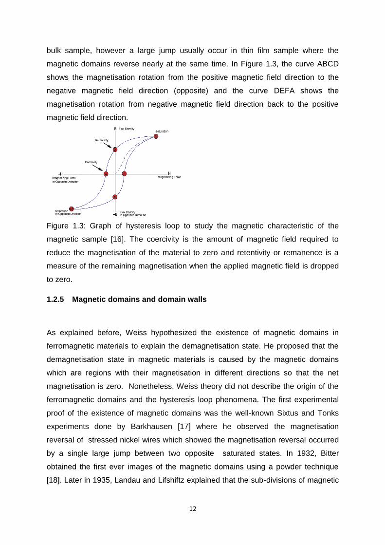
12
bulk sample, however a large jump usually occur in thin film sample where the
magnetic domains reverse nearly at the same time. In Figure 1.3, the curve ABCD
shows the magnetisation rotation from the positive magnetic field direction to the
negative magnetic field direction (opposite) and the curve DEFA shows the
magnetisation rotation from negative magnetic field direction back to the positive
magnetic field direction.
Figure 1.3: Graph of hysteresis loop to study the magnetic characteristic of the
magnetic sample [16]. The coercivity is the amount of magnetic field required to
reduce the magnetisation of the material to zero and retentivity or remanence is a
measure of the remaining magnetisation when the applied magnetic field is dropped
to zero.
1.2.5 Magnetic domains and domain walls
As explained before, Weiss hypothesized the existence of magnetic domains in
ferromagnetic materials to explain the demagnetisation state. He proposed that the
demagnetisation state in magnetic materials is caused by the magnetic domains
which are regions with their magnetisation in different directions so that the net
magnetisation is zero. Nonetheless, Weiss theory did not describe the origin of the
ferromagnetic domains and the hysteresis loop phenomena. The first experimental
proof of the existence of magnetic domains was the well-known Sixtus and Tonks
experiments done by Barkhausen [17] where he observed the magnetisation
reversal of stressed nickel wires which showed the magnetisation reversal occurred
by a single large jump between two opposite saturated states. In 1932, Bitter
obtained the first ever images of the magnetic domains using a powder technique
[18]. Later in 1935, Landau and Lifshiftz explained that the sub-divisions of magnetic
13
domains occurred in order to reduce the magnetostatic energy due to saturation in
the magnetic sample [19]. The magnetostatic energy can be evaluated as:
Equation 1.8
where is the permeability of free space. The equation presents the interaction
of dipoles with the field produced from the other dipole and is the volume
of space. The
is included to prevent from counting the interaction twice. Although
the interaction of dipoles is much weaker than the powerful exchange interaction that
occurs in short range distance, but in long range the dipoles interaction is dominant.
Therefore dipoles interaction is very important in describing the properties of
magnetic moments in long range distance that is linked to the formation of magnetic
domains specifically to reduce the magnetostatic energy. The dipoles interaction
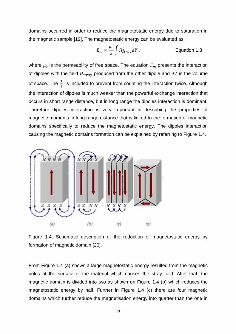
causing the magnetic domains formation can be explained by referring to Figure 1.4.
Figure 1.4: Schematic description of the reduction of magnetostatic energy by
formation of magnetic domain [20].
From Figure 1.4 (a) shows a large magnetostatic energy resulted from the magnetic
poles at the surface of the material which causes the stray field. After that, the
magnetic domain is divided into two as shown on Figure 1.4 (b) which reduces the
magnetostatic energy by half. Further in Figure 1.4 (c) there are four magnetic
domains which further reduce the magnetisation energy into quarter than the one in

14
the saturation state. And finally in Figure 1.4 (d) shows the closure of domains
structure where the net magnetisation of the material is equal to zero. Additional
divisions of magnetic domains can also occur but only up to when the energy for the
formation of each additional domain wall is greater than the reduction in the
magnetostatic energy. Therefore the size of magnetic domain also depends on this
new factor known as the magnetic domain walls which will be described later. And
lastly, more complicated magnetic domain patterns can exist in different shape
materials and different constituent of magnetic material.
1.2.6 Shape anisotropy
For a small patterned magnetic structure, the sample can be saturated along the
direction of the applied magnetic field to give a single magnetic domain of the
sample. Such sample can retain its single domain magnetisation or form sub-
divisions magnetic domains without the applied magnetic field, given that the size
and shape is less than the critical value of the material. Likewise, the formed domain
patterns characteristic is more favourable due to the shape and size of the sample
effect related to the magnetostatic energy of the sample. The shape anisotropy
energy density can be derived from the magnetostatic energy related to the stray
field produced by the magnetic dipoles on the sample surface which gives:
, Equation 1.9
where is the demagnetization factor parallel to the easy-axis, is the angle
between the easy axis and the magnetisation and stands for the demagnetization
factor perpendicular to the easy-axis of the sample. Therefore, as an example, a
nanowire wire will have its easy axis along the wire plane as this is much more
favourable due to the shape anisotropy effect for lowest energy. Other example is an
elliptical shape sample as shown on Figure 1.5 where the more favourable
magnetisation direction is along the long axis of the sample. In addition, the
saturation magnetic field is higher along the short axis than saturation magnetic field
along the easy axis due to the higher magnetostatic energy for the short axis.

15
Figure 1.5: Schematic diagram of an elliptical shaped sample showing it’s long axis
and short axis.
1.3 Different energy densities in ferromagnetic material
The energy of different magnetic domains arrangements are not only from the
magnetostatic energy contributions, but also from other different energy
contributions. The other energy contributions will be discussed in this section in
details in order to understand the generalised concept of different magnetisation
directions and different magnetic domains formations in the ferromagnetic materials.
It is also important to know the sources of the energies that influence such domains
arrangement in order to do micromagnetic calculation of the magnetisation
distribution in the ferromagnetic sample. There are five main energy contributions;
magnetocrystalline anisotropy, exchange energy, magnetoelastic energy,
magnetostatic energy and zeeman energy.
1.3.1 Magnetocrystalline anisotropy
Magnetocrystalline anisotropy describes the tendency of the magnetisation direction
of the material along a certain crystallographic directions. This preferred
crystallographic axis is called the easy axis and the direction where the
magnetisation direction is the least favourable is known as the hard axis. It is

16
experimentally proven that the hard axis has higher saturation field than the easy
axis.
Figure 1.6: Magnetisation curve of magnetite for easy and hard axis [21].
From Figure 1.6, the preferred easy axis of magnetite is the [111] axis and the hard
axis is the [100] axis. And as shown by the curve, the saturation field for the easy
axis is lower than the saturation field for the hard axis. The magnetocrystalline
anisotropy energy density for cubic crystals such as iron and nickel is:
Equation 1.10
where, and are the respective primary and secondary anisotropy constants for
the material and are the directional cosines relative to the cube edges. For
nickel, the values of and are -4.5 x 10³J/m3 and -2.5 x 10³ J/m3 respectively
[22]. And the magnetocrystalline anisotropy energy density for the uniaxial materials
such as cobalt is:
Equation 1.11
where is the angle between the easy axis and magnetisation. Experimentally, the
constants for cobalt at room temperature are: =4.1x10⁵J/m3 and =1.5x10⁵ J/m3
[23].

17
As the effect of magentocrystalline anisotropy always appear in a single crystal,
therefore in polycrystalline samples the magentocrystalline anisotropy will be
averaged throughout the random orientation of each crystallite formations. It is
proved by Bozorth that the magnetocrystalline anisotropy for nickel-iron alloys,
depends largely on the percentage content of nickel content [24]. The curve relating
the nickel content in nickel iron with the anisotropy constants of the nickel iron is
shown in Figure 1.7.
Figure 1.7: Variation of anisotropy constants of nickel iron at different percentage
content of nickel at room temperature [24]. The solid curve represents the variation
of the magnetocrystalline anisotropy constant, and the dotted line represents the
magnetocrystalline anisotropy constant, at different content of nickel in nickel iron.
1.3.2 Exchange energy
The exchange energy is the energy that keeps the magnetic moments to be aligned
parallel to each other. This is described before as the interaction energy for the short
range distance with the nearest neighbour. Therefore the energy to change the
direction of the magnetisation is called the exchange energy and is given in the form:

18
Equation 1.12
In this equation, is the exchange stiffness constant (J/m) which is temperature
dependent and are the direction cosines of the spin at lattice point .
1.3.3 Magnetoelastic energy
Magnetoelastic energy is part of the magnetocrystalline anisotropy that depends on
the mechanical strain on the material. When strain is applied to the crystal lattice, the
distances between the atoms are shifted causing change to the interaction energies
and this effect is called the magnetoelastic energy. Clearly, for a crystal lattice which
has no strain will has zero magnetoelastic energy and therefore its magnetisation is
determined by other magnetic anisotropy. With the spin-orbit coupling effect known
as magnetostriction with symbol defined for various lattice directions, the
magnetoelastic energy density is derived as:
Equation 1.13
where is the stress and is the angle between the stress direction and the
magnetisation direction. Stress in thin films and multilayer can be applied during
fabrication of sample by applying thermal stress and different lattice alignments
between layers.
1.3.4 Magnetostatic energy
The magnetostatic energy is described in the previous section and its density is:
Equation 1.14
where is the saturation magnetisation vector. As discussed previously, the
magnetostatic energy is caused by the stray field, resulted from the magnetic

19
dipole on the surface of the material. Additionally the stray field will always try to
oppose the direction of the saturation magnetisation, .
1.3.5 Zeeman energy
The Zeeman energy can be considered as the potential energy of a magnetic
moment in a field. It is the energy caused by the interaction of the saturation
magnetisation and the external applied magnetic field, therefore its energy density is
written as:
Equation 1.15
1.4 Domain walls
From the previous discussion, the existence of the magnetic domains in
ferromagnetic materials and how their specific orientations and properties are related
to the energy contributions to the ferromagnets. It have been explained that it is very
important to know that when magnetic domains exist in a region, there must be
different directions of magnetic domains. Thus, there must be walls that separate
different magnetic domains and they are known as the magnetic domain wall.
Because the formation of magnetic domains is for energy minimisation, therefore
domain walls are formed along with magnetic domains naturally. Thus, the energy of
different domain walls orientation will also be balanced with the magnetostatic
energy for having the one magnetic domain state. In general, domain wall
configuration largely depends on the minimisation of exchange and anisotropy
energy.
1.4.1 Bloch wall
Bloch wall is the transition layers between domains where the magnetisation
changes from one domain to the other. It is known that the magnetisation of Bloch
wall rotates along the axis perpendicular to the plane of the wall. Bloch walls form in

20
bulk material where the domain wall width is lot smaller than the magnetic material.
Figure 1.8 shows the Bloch wall with total angular displacement of 180ᵒ. If the Bloch
wall transition is over atomic planes, therefore for the transition, one pair of spin
will give exchange energy of:
Equation 1.16
The exchange energy density of the spin transition can be written as:
Equation 1.17
where is the exchange integral, is the spin angular momentum and is the
lattice constant of the material. Certainly if increases, the number of spin magnetic
moments aligned in the hard axis will also increase. Therefore, there will be an
increase in the magnetocrystalline anisotropy energy per unit area and it is given as:
Equation 1.18
where is the magnetocrystalline anisotropy. Furthermore, the total energy per unit
area of the Bloch wall will be calculated by summation of the exchange energy
density of the spin transition and the magnetocrystalline anisotropy energy per unit
area, which gives:
. Equation 1.19
The total wall energy per unit area is a minimum with respect to when
Equation 1.20
where is the exchange stiffness constant. The 180ᵒ Bloch wall energy density can
be obtained by substituting Equation 1.20 into Equation 1.19 and the result is:
Equation 1.21
The wall thickness is in the order of
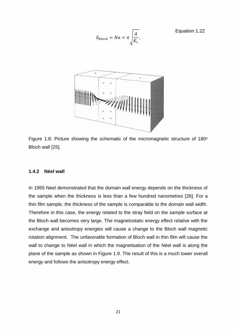
21
Equation 1.22
Figure 1.8: Picture showing the schematic of the micromagnetic structure of 180ᵒ
Bloch wall [25].
1.4.2 Néel wall
In 1955 Neel demonstrated that the domain wall energy depends on the thickness of
the sample when the thickness is less than a few hundred nanometres [26]. For a
thin film sample, the thickness of the sample is comparable to the domain wall width.
Therefore in this case, the energy related to the stray field on the sample surface at
the Bloch wall becomes very large. The magnetostatic energy effect relative with the
exchange and anisotropy energies will cause a change to the Bloch wall magnetic
rotation alignment. The unfavorable formation of Bloch wall in thin film will cause the
wall to change to Néel wall in which the magnetisation of the Néel wall is along the
plane of the sample as shown in Figure 1.9. The result of this is a much lower overall
energy and follows the anisotropy energy effect.

22
Figure 1.9: Schematic diagrams of the out of plane spin of Bloch wall and in plane
spin of Néel wall [27].
The total energy per unit area of Néel wall can be calculated by including the
exchange energy and the magnetocrystalline energy to give:
Equation 1.23
Considering zero magnetocrytsralline anisotropy constant, as for NiFe will give
Néel wall energy per unit area in the order of:
Equation 1.24
Therefore the width of Néel wall can be written as:
Equation 1.25
Figure 1.9 shows the wall energy for Bloch and Neel walls in thin films, as functions
of film thickness. From the curve, it is observed that the Bloch wall energy increases
with film thickness around less than 40 nm width but Néel wall shows a decrease in
energy causing the Néel wall to be more favourable.

23
Figure 1.20: Curves showing the energy per unit area (top) and thickness (bottom)of
a Bloch wall and a Neel wall as function of the film thickness. Parameters used are
A=10-11 J/m, Bs=1 T, and K=100 J/m3 [23].
1.5 Magnetic domains and domain walls in permalloy nanowire
As this project involves the observation of magnetic domains in nanowire, it is
essential to know the different types of domain walls formation in nanowire which
gives the distinct properties of nanowire magnetisation. The thickness of nanowires
are usually fabricated around few tens of nanometres but the axial length are
significantly large, in the order of micrometres. The typical width of nanowire is in
the order of hundreds of nanometres which is incomparably smaller than the long
axis length. Nanowires can come in different forms or shapes such as zigzag
nanowire and nanowire with notch connected to an elliptical pad. Nanowires have
simple magnetisation distribution due to the geometry of nanowire. The nanowire
magnetisations tend to align along the long axis of the nanowire due to the
magnetostatic energy and the shape anisotropy of the nanowire. The magnetic

24
moment spin of permalloy nanowires or any ultrasmall magnetic samples prefer to
be positioned parallel to the edges. Such effect is to reduce the magnetostatic
energy of the nanowire and this agrees with the experimental results [28] shown in
Figure 1.21.
Figure 1.21: Fresnel images taken showing the distribution of magnetization within
the samples. The overall length of all elements is 2.5 µm. In (b), white arrows mark
the inner corners of element tips and n (d) white arrow marks the near end
structures. The black arrows in (e) mark parts of the edge normal to the element
length and close to the element end [28].
As a result of the shape anisotropy and the spin alignment parallel to the edge of
sample, in elliptical pad the magnetic moments form a vortex as they follow the
elliptic pattern of the sample edges. This caused the saturation field of the elliptical
pad to be lower than a nanowire sample because by forming a vortex, it helps to
reduce the energy for saturation magnetisation. Both theories are proven with the
experimental results in [29].

25
Domain wall formation can be divided into two; the tail-to-tail and head-to-head
domain walls depending on the ‘head’ or ‘tail’ side of the magnetic moment as shown
on Figure 1.22.
Figure 1.22: Schematic of the head-to-head and tail-to-tail domain walls.
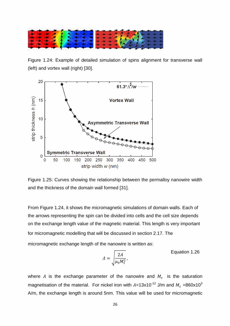
There are three different domain walls structure; the transverse wall (TW), the vortex
wall (VW) and the asymmetric transverse wall which is an intermediate state
between the first two walls. The three different domain walls are shown in Figure
1.23 and simulation diagrams of the TW and VW are shown in Figure 1.24 [30] to
demonstrate the detailed structure of magnetic moments in each wall. As the width
and thickness of the nanowire is increased, a symmetric transverse will become
distorted causing it to be asymmetric and thus forming the asymmetric transverse.
Further increase in the nanowire width and thickness will increase the chance of the
formation of vortex wall. Domain walls possess chirality where the magnetisation
head or rotation can be either up or down. Chirality characteristic of domain walls is
shown in Figure 1.23 where in the VW the rotation changes from clockwise to anti-
clockwise. In a symmetric nanowire, different chiralities have equivalent energy
state. Figure 1.25 from Nakatani [31] can be used to determine the type of domain
walls at different wire widths and thickness.
Figure 1.23: Different types of domain walls with chirality.
26
Figure 1.24: Example of detailed simulation of spins alignment for transverse wall
(left) and vortex wall (right) [30].
Figure 1.25: Curves showing the relationship between the permalloy nanowire width
and the thickness of the domain wall formed [31].
From Figure 1.24, it shows the micromagnetic simulations of domain walls. Each of
the arrows representing the spin can be divided into cells and the cell size depends
on the exchange length value of the magnetic material. This length is very important
for micromagnetic modelling that will be discussed in section 2.17. The
micromagnetic exchange length of the nanowire is written as:
Equation 1.26
where is the exchange parameter of the nanowire and is the saturation
magnetisation of the material. For nickel iron with =13x10-12 J/m and =860x103
A/m, the exchange length is around 5nm. This value will be used for micromagnetic
27
simulation to determine the cell size for the micromagnetic simulation of nickel iron.
For a nanowire patterned with notch as what is going to be done for this project, the
spin at the notch will align along the edges of the notch. The notch will change the
domain walls nature in the nanowires by trapping and pinning.
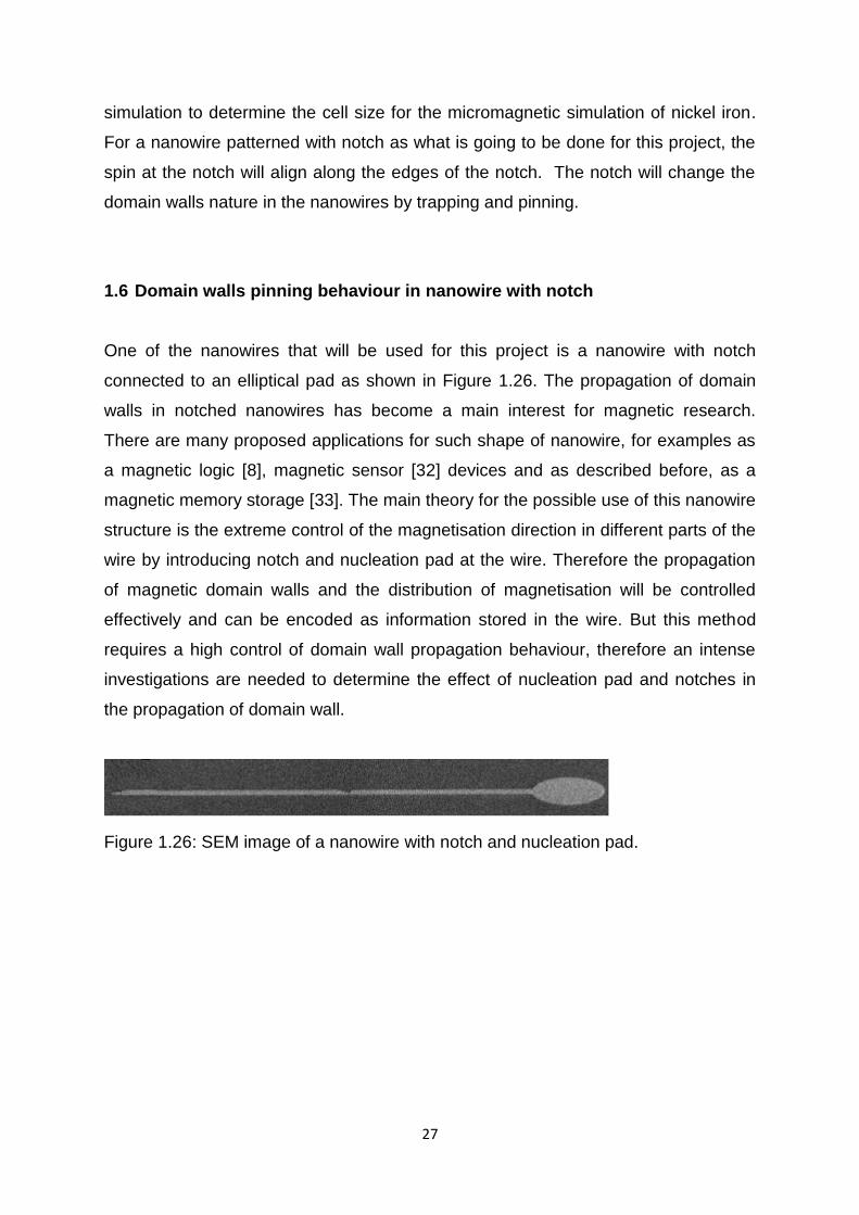
1.6 Domain walls pinning behaviour in nanowire with notch
One of the nanowires that will be used for this project is a nanowire with notch
connected to an elliptical pad as shown in Figure 1.26. The propagation of domain
walls in notched nanowires has become a main interest for magnetic research.
There are many proposed applications for such shape of nanowire, for examples as
a magnetic logic [8], magnetic sensor [32] devices and as described before, as a
magnetic memory storage [33]. The main theory for the possible use of this nanowire
structure is the extreme control of the magnetisation direction in different parts of the
wire by introducing notch and nucleation pad at the wire. Therefore the propagation
of magnetic domain walls and the distribution of magnetisation will be controlled
effectively and can be encoded as information stored in the wire. But this method
requires a high control of domain wall propagation behaviour, therefore an intense
investigations are needed to determine the effect of nucleation pad and notches in
the propagation of domain wall.
Figure 1.26: SEM image of a nanowire with notch and nucleation pad.

28
2. Experimental Method
2.1 Introduction
There are a lot of methods to observe magnetic domains but the classical Magneto-
optical Kerr effect (MOKE) technique is the most versatile and has more advantages
in comparison to other methods. MOKE is an effect when light reflected from a non-
transparent magnetic sample can change in either polarisation or reflected intensity
depending on the type of MOKE present in the sample. The types of MOKE will be
discussed later in this chapter. Although the magnetic domain contrast is very weak,
it can be enhanced by using digital image processing. Therefore, the development of
digital image processing helps to increase the effectiveness of this method. With the
many available image processing software products such as Matlab and LabVIEW,
there are a lot of different ways of enhancing the weak domain contrast in the
magnetic sample. Additionally, there is no special treatment needed for the sample
to be observed under Kerr effect microscope. Coating of the sample is allowed and
sometimes this is done to enhance the MOKE signal using dielectric coating [34].
The sample can be cooled in cryostats or heated using optical heating stages
therefore the temperature effects of the magnetic sample can be observed. Applying
physical stress to the sample is possible while doing the observation, therefore
making possible to study the stress effect on magnetic domains. The Kerr
microscope can be changed easily to study the in-plane or out-of–plane
magnetisation components of the sample. Investigation of the magnetic domains on
the sample is done directly while applying magnetic field to the sample and domain
wall motion can be observed using this method effectively.

29
2.2 Other methods
In addition to magneto-optical Kerr microscopy, there are other methods of observing
magnetic domains. Nowadays, with the plenty of existing microscopic probes with
the capability of imaging magnetic domains in very small magnetic structures such
as Lorentz microscopy [35], electron holography [35, 36] and also scanning electron
microscopy with polarisation axis [37]. Although they are capable of detecting
magnetism in a very small sample (up to nano-scale), but due to their limitation of
applying and freely modifying magnetic field inside an electron microscope, hence
studies of magnetism for the samples are limited. Other example is the Transmission
Electron microscopy (TEM), which is known to have a smaller field of view than the
Kerr microscope. However for other microscopes that do not utilize the electron
microscope such as magnetic force microscopy, spin-polarised tunnel microscopy
[38] and other resonant technique [39], there are also other limiting factors that
restrain their capability to observe magnetism such as the in situ preparation
requirement for the spin-polarised tunnel microscopy. Alternatively, there are other
high advance magnetometry techniques that have been developed and are capable
of observing magnetism in nano-scale magnetic samples for example Hall-probe
technique and nano Superconducting Quantum Interference Devices (SQUID) [40].
Despite the advantages, unfortunately these techniques need the fabrication of
specialized sample, meaning they are not compatible with other general samples
and sample shapes. In general, a technique which is very flexible, versatile, non-
destructive to the sample and capable to detect magnetisation in small structures
remains as the most desired method of study. Besides having all the desired criteria,
MOKE is the least expensive method of study available compared to the other
techniques mentioned earlier.
2.3 Magneto-optical Kerr effect
Kerr effect is an effect when a linearly polarised light reflects from a magnetic
sample, its polarisation axis becomes rotated and at the same time, it is elliptically
rotated. It was first reported by John Kerr in 1877 [41], but similar effect was first

30
discovered by Faraday in 1845 [42] where he found out that the plane of polarisation
of light transmitted through a magnetic sample was rotated. The angle of rotation of
polarisation observed for both effects depend on the strength of the magnetisation of
the surface of the sample and the magnetisation orientation of the sample surface
with respect to the plane of light incidence. This influence of the magnetisation
orientation can be described by the different magnetisation geometries of Kerr effect.
The rotation effect of MOKE can be described generally in the form of dielectric
tensor which account for the effect of magnetic medium. The dielectric law is given
as:
Equation 2.1
In Equation 2.1, is the dielectric permittivity tensor which connects the electric field
vector of the plane of light wave along with , the induced electrical displacement
vector. The generalized dielectric permittivity tensor is given in [43] in the form of:
Equation 2.2
where is the Voigt constant in which it is material dependent that describes the
magneto-optical rotation of the plane of polarisation of light, in this case the reflection
in the Kerr effect. This Voigt term is a complex material parameter that is to the first
order proportional to the magnetisation of the sample. and are constants
describing the Voigt effect and are the components of the unit vector of
magnetisation along the cubic axis. , and are very complex and are not well
known for the majority of materials, but the real parts of these constants are the most
dominant. By using the term in Equation 2.1 the dielectric law can be generalised as
shown in [44]:
Equation 2.3

31
In Equation 2.2, is the dielectric permittivity tensor, vector represents the
secondary light amplitude which is produced by the magneto-optic interaction
between and the magnetisation vector in the sample. From Equation 2.3, the
cross product proves the gyroelectric nature of the Kerr effect with its symmetry
which can be explained using the Lorentz force ( theory. In general, what
being observed in MOKE is the magneto-optic response of the medium which is in
the form of change in the polarisation of the incident light. This change is made of
two types, the change of the in-phase component of the reflected light causing
rotational change in the plane of polarisation of the incident light and the out-of-
phase change which cause the elliptical change to the polarisation of incident light.
2.4 Geometries of Kerr effect
There are three different geometries of MOKE where their differences are relative to
the plane of light incidence. The three different geometries of MOKE are shown in
Figure 2.1 which consists of the polar MOKE, longitudinal MOKE and transverse
MOKE.
Figure 2.1: Schematic to show the three different magnetisation orientations (a)
longitudinal, (b) transverse and (c) polar orientations the Kerr effect can be
observed.
32
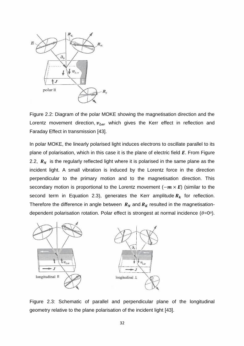
Figure 2.2: Diagram of the polar MOKE showing the magnetisation direction and the
Lorentz movement direction, which gives the Kerr effect in reflection and
Faraday Effect in transmission [43].
In polar MOKE, the linearly polarised light induces electrons to oscillate parallel to its
plane of polarisation, which in this case it is the plane of electric field . From Figure
2.2, is the regularly reflected light where it is polarised in the same plane as the
incident light. A small vibration is induced by the Lorentz force in the direction
perpendicular to the primary motion and to the magnetisation direction. This
secondary motion is proportional to the Lorentz movement ( ) (similar to the
second term in Equation 2.3), generates the Kerr amplitude for reflection.
Therefore the difference in angle between and resulted in the magnetisation-
dependent polarisation rotation. Polar effect is strongest at normal incidence ( =0ᵒ).
Figure 2.3: Schematic of parallel and perpendicular plane of the longitudinal
geometry relative to the plane polarisation of the incident light [43].

33
For longitudinal geometry, the magnetisation direction of the sample is parallel to the
plane of light incidence. The longitudinal effect induces rotational change to the
plane of polarisation for both parallel polarisation and perpendicular polarisation
plane of incident light. From Figure 2.3, the Lorentz motions in the two different
polarisation of the plane of incidence are opposite to each other giving rise to
opposite rotational direction of the resulting Kerr amplitude. Longitudinal effect
disappears for normal light incidence ( =0ᵒ) as the Lorentz force either vanishes or
points along the beam.
Figure 2.4: Sketch of the transverse MOKE with the Lorentz movement [43].
Transverse MOKE occurs when the magnetisation direction is perpendicular to the
plane of light incidence. As shown in the
Figure 2.4, the transverse effect cause amplitude change to the reflected light but the
polarisation direction of the Kerr amplitude is the same as that of the regularly
reflected light. Thus, it will produce little contrast in the resulting image as there will
also be noise in the form of intensity change from the light source which can affect
the transverse MOKE signal. Yet the transverse MOKE can be used for measuring
function [45]. Similar to the longitudinal MOKE, the transverse effect is eliminated in
normal light incidence to the sample surface.

34
Figure 2.5: Schematic diagram showing the superpositions of the p-polarised light
(P-light) and s-polarised light (S-light) of the incident light.
The explanation for longitudinal and transverse Kerr effect above can be simplified
by using the Kerr Fresnel reflection coefficient that has been obtained by applying
Maxwell boundary conditions at surface films [46]. Referring to Figure 2.5 which
shows the superposition of the p-polarised and s-polarised light that is incident to the
surface and then gets reflected, the coefficients for transverse as given in [47] are
given by Equation 2.4, 2.5 and 2.6 and written as:
Equation 2.4
Equation 2.5
Equation 2.6
And the Fresnel reflection coefficients for the longitudinal Kerr effect [47] are:
Equation 2.7
Equation 2.8

35
Equation 2.9
where is the angle of incidence measured from the normal of the sample, is the
index of refraction of the film, is the off diagonal element of the relative
permittivity tensor, , and
. Referring to the
transverse coefficients above, the transverse Kerr effect does not cause rotational
change to the plane of polarisation of the incident light given that the off-diagonal
terms which cause the rotational are equal to zero as shown in Equation 2.6. The
only parameter that is magnetisation-dependent is the reflection coefficient relating
the incident and reflected p-polarised light given in Equation 2.4. Therefore there will
only be light intensity change for transverse effect as explained previously. Further,
for longitudinal Kerr effect, the coefficients confirm that there is a magnetic-
dependent rotational change to the plane polarisation of the incident light by the
derived off-diagonal terms in Equation 2.9.
The light intensity, after passing through the analyser can be presented using the
normal polarisation equation in the form of:
Equation 2.10
where is the intensity of the reflected light before entering the analyser and is
the angle between the plane polarisation of and the plane of analyser. Hence, the
maximum intensity change can be calculated by differentiating Equation 2.10, which
gives:
Equation 2.11
The resulted maximum change of intensity is at , but this is the maximum
change of the whole reflected light. A change of the light intensity caused by the Kerr
rotation which is relative to the whole reflected light is needed and shown as:
Equation 2.12
Hence, the relative change due to the Kerr rotation is:

36
Equation 2.13
and is:
Equation 2.14
where is the light intensity change due to Kerr rotation and is the angle of Kerr
rotation. Furthermore, by plotting the graph in Figure 2.6 relating the Kerr sensitivity
and the analyser setting as shown in Equation 2.14, it is demonstrated that the
is very high in the regions of analyser setting near to 90ᵒ.
Figure 2.6: Graph of Kerr sensitivity versus the angle between the plane polarisation
of the polariser and the plane of analyser.
As seen in Figure 2.6, the high slope of the graph at 90ᵒ means a slight change in
the angle of analyser can cause a high gain or loss of Kerr sensitivity.
Experimentally, it is hard to pinpoint the analyser angle by a few degrees. Moreover,
there is always a degree of imperfection to the polarized light [48] because of the
polarizers being less than 100% efficient and to the range of angles of incidence in
the focused beam on the sample. Therefore it is impossible to set the analyser
exactly at 0ᵒ cross with the polariser to completely remove the background light for a
very high Kerr sensitivity.
37
In order to get high Kerr sensitivity, it cannot always be achieved by setting the
analyser and the polariser to be perfectly crossed or trying to remove much of the
background light through extinction as discussed above. If the resulted image is too
dark, the signal processed electronically will be too small. The resulted dark image
captured by the camera will contain less Kerr signal as it is very dim, therefore larger
analyser angle is more favoured. Similarly, for a high Kerr sensitivity microscope
setup, the signal-to-noise ratio, of the Kerr microscope needs to be high enough
so that the weak Kerr signal is not lost in the noise. Kerr signal is very weak but it
can be enhanced electronically on condition that the is large enough.
2.5 Wide-field Kerr microscope set up
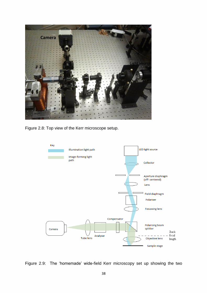
The first part of the experiment was to build a ‘homemade’ wide-field Kerr
microscope on an optical table. The wide-field Kerr microscope built is based on the
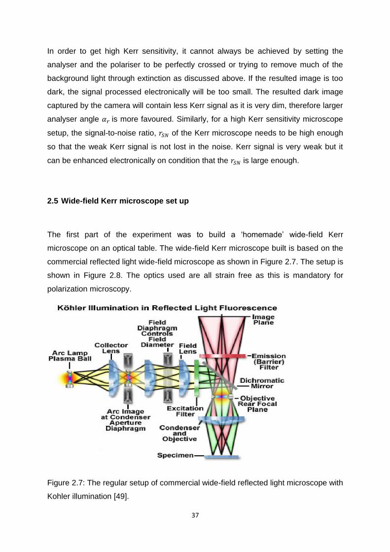
commercial reflected light wide-field microscope as shown in Figure 2.7. The setup is
shown in Figure 2.8. The optics used are all strain free as this is mandatory for
polarization microscopy.
Figure 2.7: The regular setup of commercial wide-field reflected light microscope with
Kohler illumination [49].
38
Figure 2.8: Top view of the Kerr microscope setup.
Figure 2.9: The ‘homemade’ wide-field Kerr microscopy set up showing the two
Camera
Light source

39
different light paths, the illumination light path and the image-forming light path. The
setup is the off-centered aperture sensitivity setup for longitudinal Kerr effect and
also transverse Kerr effect.
2.6 Optics
As shown on Figure 2.9 the light source used for this setup is a LED lamp. When the
light passes through the collector, it focuses the light to the iris of the aperture
diaphragm. Aperture diaphragm is crucial in Kerr microscopy setup and will be
looked at later in this chapter. The second lens in the setup change the light rays to
infinity as it passes through the field diaphragm and the polariser. Then, the
focussing lens will focus the light to the back focal plane of the objective lens.
Further, the light is collimated by the objective lens to illuminate the magnetic sample
on the sample stage.
The light illuminated on the sample is then reflected along with the changes due to
the Kerr effect. The changes involved are polarisation, intensity change and phase
change depending on the type of MOKE that occurs in the magnetic sample.
Subsequently, the reflected light is reflected by the polarising beamsplitter away from
the illumination light path. Thus, the light together with the changes goes through the
compensator and analyser. The compensator used in the setup is a quarter wave
plates. The analyser translates the plane polarisation change into an intensity
change and the image is focused on the CCD chip by the tube lens. It can be noticed
from Figure 2.9 the light is projected to infinity as it passes through the polariser,
compensator and analyser. In account for this is that at infinity light rays, these optic
components will not distort the image.
Before the polarising beamsplitter was used, the original reflector that had been used
was a non-polarising beamsplitter. This beamsplitter has a splitting ratio of 50:50,
resulting in a 50% light loss from the light source and an additional 50% lost after it is
reflected to the compensator. As explained earlier, signal-to noise ratio depends on
the illumination intensity, therefore this loss is unbearable as this will lead to an
image with a very low Kerr signal and very dim (dark image). Kerr effect is already

40
too small to be observed, this large amount of light loss will further reduce the Kerr
sensitivity of the setup. The reflector was later replaced with polarising beam splitter
with transmission percentage of 90% P-polarised light and reflectance percentage of
99.5% of S-polarised light. Therefore the plane of incident light is a P-polarised light
and thus, the plane of polariser needs to be aligned along the P-polarised light as
required for Kerr microscopy.
The polarizer and analyser are set to nearly perpendicularly crossed with each other
for the polar and longitudinal Kerr effect. This is to get the maximum extinction in one
of the domain for an optimum magnetic domain contrast. For transverse effect, a
‘longitudinal with transverse sensitivity’ setup is applied and a way to do this will be
explained later in this chapter. This setup utilizes a Glan-Taylor prism as the
polariser and analyser. This polarizer has an extinction ratio of greater than 105:1,
which is high enough for the observation of the weak Kerr effect.
2.7 Sources of noise
For the overall setup for Kerr microscopy the sources of noise that are taken into
account are;
1) The shot created by the quantized nature of light, this is an inevitable noise which
varies with the photon number in the image.
2) Electronic noise that is independent of the image intensity caused by the
instruments and the detection electronics.
3) Fluctuation of the light source and in the sample which are proportional to the
image intensity.
4) Stability noise of the overall microscope setup, especially when observing nano-
sized samples where nanometre movement of the sample during the experiment can
cause significant noise contribution in the image and even worse, the loss of signal.

41
As the shot noise is the unavoidable noise, it preferable to take into consideration the
relative signal-to-noise ratio caused by this noise. Also this can be used to represent
the overall noise in the microscopy setup. A method in [43] show; that the shot noise
can be written as
, where is the number of photons
illuminating the sample, is the intensity of dark magnetic domain in the image and is
the intensity of the other magnetic domains in the image. Again, simplified from [43],
the optimum value of the analyser angle in relation to the signal-to-
noise ratio and the optimum signal-to-ratio are:
Equation 2.15
Equation 2.16
Here, is the regular amplitude, is the magneto optical amplitude (effective Kerr
amplitude) and is the background intensity. This proves that the maximum value of
signal-to-noise ratio depends on the Kerr amplitude and the number of illuminating
photon, however it is not determined by the Kerr rotation. Therefore, it is important to
maximize the illumination intensity on the sample and the use of a powerful light
source is important. Further addition of the electronic noise, fluctuation noise and
other noise reduces the signal-to-noise ratio but overall it does not affect the
essential feature of the explanation above.
2.8 Light source
The light source used was a royal blue LED light with a wavelength of 455 nm. The
first light source used was a tungsten lamp, although it can produce very bright light,
it gets heated up very quickly and there was no ventilated lamp house with fan heat
sinks to remove the heat generated by this bulb. And, in comparison to the LED, the
tungsten lamp gives out a less stable light source. At some point, a laser was utilized
into the setup as a light source but laser illumination introduces speckles and

42
hotspots in the image. To reduce the formation of hotspots and speckles on the
image, a rotating plastic disc was inserted in front of the laser source. The speed of
the spinning plastic disc can be controlled throughout the experiment. In part a of
Figure 2.10, the result shows an image with hotspots and speckles that are highly
prevalence even after placing the rotating plastic disc into the setup. There are a
number of ways to reduce the speckles and hotspots [50] however the LED was
chosen for its well-defined output image and optimized thermal management. The
difference in the quality of image produced by using laser and LED as a light source
can be seen in Figure 2.10.
Figure 2.10: Images of nanowires with width around 380 nm with nucleation pad
under the microscope using two different light sources, the figure on the left shows
the image produced by using laser as the light source (a) with the introduction of
rotating plastic disk whereas the image on the resulted from using LED (b).
2.9 Kohler illumination and field diaphragm
Wide-field microscopes use the Kohler illumination technique. Kohler illumination is a
method of sample illumination where the purpose is to obtain an incredibly even
illumination of the sample and that the image of the illumination source (light source)
is not present in the resulting image. In most modern microscopes, the Kohler
illumination is used and no construction of this technique is needed. But, to build a
‘homemade’ microscope, this part is very vital as uniform illumination is needed for
Kerr effect observation. To achieve Kohler illumination, the light emitted from the
a b

43
light source must be focussed at the back focal plane of the objective lens, as a
result the illuminating light rays goes to infinity, thus giving Kohler illumination to the
surface sample. From Figure 2.9 the focussing lens is used to focus the light rays at
the back focal length of the objective lens and at the same time it imaged the field
diaphragm is imaged on the sample surface. This can be seen on part b of Figure
2.10 where the field diaphragm image can be seen on the resulted image and it
limits the area of the sample to be illuminated by blocking the undesired light rays.
In conclusion, the position of the back focal plane of the objective lens is required for
Kohler illumination. However, the position of the back focal length is classified
information as different companies have their own ‘secret ingredients’ in their
commercial microscope which remain unrevealed. An attempt was made to try to
contact the main office of the manufacturer of the objective lens asking them for the
distance value of the back focal length, however they denied my request as the back
focal length value of their objective lens is classified. Therefore the value was
calculated manually and this is illustrated by the ray diagram in Figure 2.11 . The
focussing lens with a known focal length is moved forward and backward while the
illuminated light is confirmed for infinity rays. To check for infinity rays, the size of the
light spot must be the same size near the output of the objective lens and at another
distance about two feet away from the objective lens. After this is accomplished, the
focussing lens is locked at that position and as shown in Figure 2.11 the field
diaphragm is fixed at the back focal length of the focussing lens to image the field
diaphragm into the resulting image. The resulted back focal length value is so
different that it is not equal to the calculated value using the back focal length
equation ( which is caused by the unique internal design of the
microscope.
44
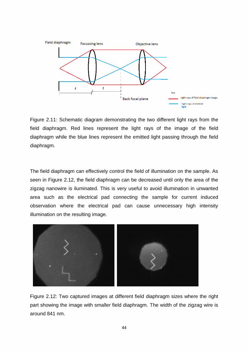
Figure 2.11: Schematic diagram demonstrating the two different light rays from the
field diaphragm. Red lines represent the light rays of the image of the field
diaphragm while the blue lines represent the emitted light passing through the field
diaphragm.
The field diaphragm can effectively control the field of illumination on the sample. As
seen in Figure 2.12, the field diaphragm can be decreased until only the area of the
zigzag nanowire is iluminated. This is very useful to avoid illumination in unwanted
area such as the electrical pad connecting the sample for current induced
observation where the electrical pad can cause unnecessary high intensity
illumination on the resulting image.
Figure 2.12: Two captured images at different field diaphragm sizes where the right
part showing the image with smaller field diaphragm. The width of the zigzag wire is
around 841 nm.

45
2.10 Aperture diaphragm
The aperture diaphragm is one of the most crucial parts of the Kerr microscope. In
normal microscope, the aperture diaphragm controls the optical resolution and
intensity of illumination. The smaller the size of the aperture diaphragm, the higher
the resolution of the image but the lower the intensity of illumination will be and
increasing the aperture size will reduce the resolution but the illumination intensity
will increase. The same effects also occur in Kerr microscopy with some additional
effects. The additional effects are; closing and opening the aperture diaphragm
change the angle of incidence, and moving the aperture diaphragm off-centered
depending on which direction it moves to, determines the type of MOKE the
microscope will observe. Therefore, the aperture determines the angle of incidence
with the largest angel of incidence being limited by the numerical aperture of the
objective lens. This shows the fundamental role of the aperture diaphragm in the
Kerr microscope setup.
In Figure 2.13, this image is the conoscopic image of the microscope. In a modern
microscope this can be seen by replacing the eyepiece with the auxiliary telescope
or with the build in Bertrand lens. But in the setup, additional lens is inserted in front
of the camera that has the right focal length to focus the back focal plane of the
objective lens to the camera. The cross-shaped image describes the extinction zone
when the polariser and the analyser are crossed (crossed polarised) for maximum
extinction in the sample image. The cross-shaped is also known as the Maltese
cross and the main reason for this event to happen is because light bundle converge
in wide-field microscopy. Light rays that is not in the cross part cannot be terminated
because they are reflected in an elliptical and rotated polarised condition. Therefore
for maximum contrast results, the aperture stop is positioned in the dark (cross) area
as shown in Figure 2.13.

46
Figure 2.13: Diagram showing the extinction cross and aperture stop positions for
different MOKE geometry [44].
Further if the aperture iris is set to the centre, the whole alignment is straight and the
angle of incidence will be zero degree because this results in an illumination cone
that hits the sample cone vertically. Due to symmetry, Kerr amplitudes resulting from
the in plane magnetisation (longitudinal and transverse MOKE) components cancel
each other and the net Kerr amplitude will be zero. Consequently, in this setup, the
sensitivity is to the out-of-plane magnetisation in which as described earlier is for the
polar Kerr effect. The aperture location for polar Kerr effect is shown in Figure 2.13
and is as illustrated to be in the middle and round shape. An off-centered aperture
iris gives an obliquely incident bundle of rays which is required for longitudinal and
transverse Kerr sensitivity. The aperture locations for the longitudinal and transverse
Kerr effects are shown in Figure 2.13. In the setup, an adjustable square slit is used.
For longitudinal Kerr sensitivity, a square aperture with adjustable size is used.
Because the longitudinal Kerr effect can only be detected in oblique incidence, the
square aperture is positioned off-centered at one arm of the maltese-cross. This
gives an incident light with its plane parallel to the magnetisation direction of the
sample. Let’s simply call the transverse magnetisation in this same sample to be the
‘transverse axis’ of the sample. Therefore, changing the aperture stop to the
‘longitudinal with transverse sensitivity’ will change the plane of the incident light to
be parallel to the magnetisation direction along the ‘transverse axis’ of the same
sample. This gives the ‘transverse axis’ a magnetic contrast by using longitudinal
Kerr effect. It is better to use the longitudinal with transverse sensitivity setup for
observing transverse effect than the other two transverse setups in Figure 2.13, for
47
obvious reason that the longitudinal effect gives a stronger magnetic domain contrast
than transverse effect, as the transverse effect has higher noise because the Kerr
signal is from the light intensity change where much of the light source noise goes in
with the result. Whereas in longitudinal sensitivity the polariser and analyser are
cross-polarised near to extinction where most of the unwanted signal is removed. In
addition to that, this saves time to focus mainly on the longitudinal setup to observe
both the longitudinal and transverse Kerr effect.
2.11 Compensator
As explained before, the plane of polarisation of the reflected light is not just rotated
but also elliptically polarised. If the elliptical polarisation is more dominant than the
linear polarisation of the reflected light, a compensator is used to remove the
elliptical component and convert it into a linear wave. In this setup, a quarter-wave
plate is used as the compensator in which it must be aligned along the analyser
plane. However, using a compensator is not always necessary because oblique
incidence (light incident not at normal incident) can create a phase shifts by rotating
the polariser away from symmetry positions. Meaning, the polariser and the analyser
can be adjusted simultaneously until the desired contrast and brightness is achieved.
In the setup, it utilizes the use of longitudinal Kerr effect even for the transverse
effect, the longitudinal with transverse sensitivity is used as explained above. The
elliptical polarisation effect was observed experimentally using the Kerr microscopy
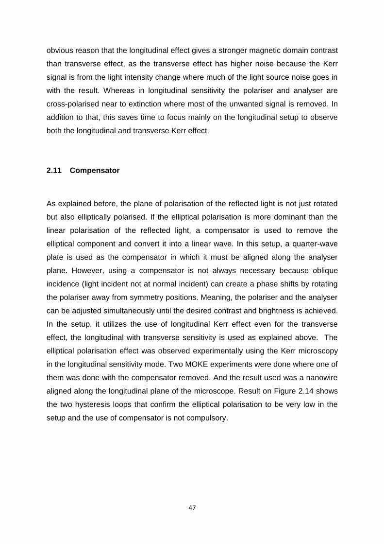
in the longitudinal sensitivity mode. Two MOKE experiments were done where one of
them was done with the compensator removed. And the result used was a nanowire
aligned along the longitudinal plane of the microscope. Result on Figure 2.14 shows
the two hysteresis loops that confirm the elliptical polarisation to be very low in the
setup and the use of compensator is not compulsory.
48
Longitudinal w ithout quarter w ave plate
Magnetic field(Oe)
-250 -200 -150 -100 -50 0 50 100 150 200 250 300
-1.0
-0.5
0.0
0.5
1.0Longitudinal w ith quarter w ave plate
Magnetic field(Oe)
-250 -200 -150 -100 -50 0 50 100 150 200 250 300
Inte
nsity (
arb
. units)
-1.0
-0.5
0.0
0.5
1.0
Figure 2.14: Two hysteresis loops from two experiments where one of them is done
with a compensator in the set up and the other one without the compensator in the
setup. The loops are results from averaging of 10 loops from sample of around 350
nm width nanowire.
2.12 Lateral Resolution and magnification of objective lens
Resolution is a very important parameter when doing microscopy given that domain
structures have different sizes down to nanometres. Because resolution is limited
due to the diffraction limit, the sample to be observed must not be smaller than the
resolution of the microscope. The lateral resolution in a microscope is dependent on
the value of the numerical aperture of the objective lens and it is written as:
Equation 2.17
where is the refractive index of the medium and is the half angle of the cone of
light from the specimen received by the objective. The minimum distance between
two points that can be resolved is given by:
Equation 2.18
where is the wavelength of the light source. In the microscope setup, the of the
objective lens is 0.55 and by assuming c to be 0.61 and together with the light
Magnetic field (Oe) Magnetic field (Oe)
Longitudinal with quarter wave plate Longitudinal without quarter wave
plate

49
source wavelength of 455 nm, the resolution of the microscope is 505 nm. 505nm is
the resolution limit of the setup, but a smaller sample up to 245 nm can also be
observed and its Kerr contrast can be made visible by doing digital contrast
enhancement. For sample smaller than the resolution limit, the sample image is
broadened and this can be seen in the results chapter of this thesis.
The total magnification of microscope may be controlled by the tube lens but this
does not change the resolution of the microscope. In other words, the image field of
the microscope can be increased or decreased by changing the magnification.
The equation for magnification is given as;
Equation 2.19
where is the focal length of the tube lens and is the focal length of the objective
lens. The tube lens focal length is 200mm and the objective lens focal length is 4
giving a 50 times magnification (50x). For nano sized samples, increasing the
magnification can increase the amount of pixel surface area on the detector chip of
the camera. But during the experiment study, only the tube lens can be changed
because there is not much option for the objective lens choice. A 500 mm tube lens
was used giving the magnification 125x. The resulted image was significantly
enlarged. With this new change in the setup, a MOKE experiment was done on the
nanowire, but unfortunately the resulted hysteresis loop was very noisy with very
small Kerr effect signal. It is deduced that, due to the very long focal length (500 mm)
of the tube lens giving an extra 300 mm distance between the tube length and the
camera have caused a lot of light loss. Further, the significantly enlarged image also
cause the loss of image brightness at the camera compared to the non-enlarged
image.
Due to the fact that this is a ‘homemade’ microscope, it is extremely important to
make sure the optimum performance of the objective lens. Due to the specific design
of the objective lens, the distance between the tube lens and the objective lens is
limited to a certain value. This is to ensure the optimum optical performance of the
objective lens and to avoid formation of shadows in the resulting image. The
equation of is given as:
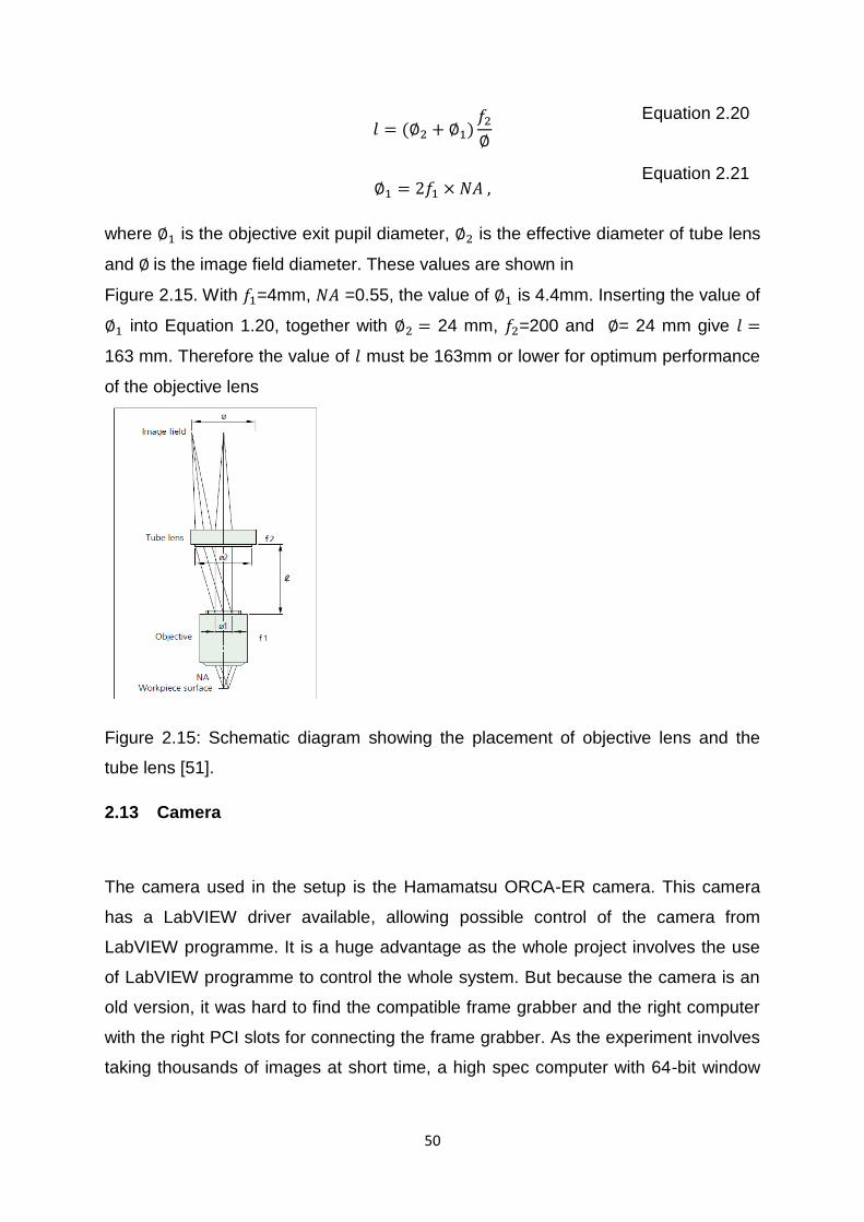
50
Equation 2.20
Equation 2.21
where is the objective exit pupil diameter, is the effective diameter of tube lens
and is the image field diameter. These values are shown in
Figure 2.15. With =4mm, =0.55, the value of is 4.4mm. Inserting the value of
into Equation 1.20, together with 24 mm, =200 and = 24 mm give
163 mm. Therefore the value of must be 163mm or lower for optimum performance
of the objective lens
Figure 2.15: Schematic diagram showing the placement of objective lens and the
tube lens [51].
2.13 Camera
The camera used in the setup is the Hamamatsu ORCA-ER camera. This camera
has a LabVIEW driver available, allowing possible control of the camera from
LabVIEW programme. It is a huge advantage as the whole project involves the use
of LabVIEW programme to control the whole system. But because the camera is an
old version, it was hard to find the compatible frame grabber and the right computer
with the right PCI slots for connecting the frame grabber. As the experiment involves
taking thousands of images at short time, a high spec computer with 64-bit window

51
was needed. The whole processes of ordering, testing and returning the frame
grabber and the computer took more than two months.
Different camera has different spectral response characteristic and it is described
using the graph of quantum efficiency versus the wavelength of the light source.
Figure 2.16 shows the spectral response characteristic of the ORCA-ER camera for
different light wavelength. Thus, one can see that the quantum efficiency of the light
source (with wavelength of 455 nm as described before) for the setup is around 68%
which is close to the optimum quantum efficiency of the camera at 72%. To detect
the weak Kerr effect, a high spectral response of the camera is needed and this
camera has that requirement.
Figure 2.16: Spectral response graph of the ORCA-ER camera [52].
2.14 Electromagnet
The electromagnet used in the setup has a limit of 2.8k Oe with poles separation of
27 mm and shown in Figure 2.17. The magnetic field strength is controlled by a
LabVIEW programme in a computer. A 1000 W amplifier is used as the power supply
for the electromagnet. The voltage output signal from the LabVIEW is connected to
the amplifier, the amplifier then converts this signal into the required power to the
electromagnet and the electromagnet will produce the required magnetic field. The
amplifier has bi-polar ability, therefore it can produce positive and negative field

52
depending on the sign of the output voltage signal from the computer. The magnet
has magnetic field of around 1700 Oe and -1700 Oe the value of amplifier input
voltage and magnetic field are directly proportional to each other. Therefore,
between these values, any change in the amplifier input value will cause a directly
proportional change in the magnetic field strength. This will be very useful when
developing LabVIEW programme for the setup and it will be explained later in this
chapter.
Figure 2.17: Shows the value of the electromagnet where the distance in between
poles is around 27 mm.
2.15 Programming
For the project, three LabVIEW programmes were created with three different roles.
A significant amount of time was spent to create these programmes to make sure
they functioned well. All the programmes were created to be as user-friendly as
possible making them very flexible and easy to understand for further development.
The programmes are:
1) Programme for taking a sets of pictures with known magnetic field for each
picture.
2) Programme to analyse the sets of images and to do digital contrast
enhancement.
3) Programme to extract the hysteresis loop for the magneto-optical
magnetometry.

53
The programmes were divided into three because the work will involve taking
thousands of pictures and saving them in the hard drive and reading thousands of
images at a fast rate. Therefore with different purpose of each programme, it is
better to separate them into three to avoid the computer from crashing as this had
happened previously.
2.15.1 Taking sets of images in loop.
The programme is divided into two parts. The first part which is on the left side of
Figure 2.18 is to set the camera setting for different functions available in it. The
functions that come with the camera are the exposure time setting, binning functions
and more. After the desired setting is chosen, the image can be viewed in video form
before starting the experiment. It is extremely important to avoid saturated pixels in
the image because the area with saturated pixels will have no data at all. This can be
seen when there is a bright white spot in the image when viewing the sample before
the experiment. It can also be checked using the saturation option tool in the camera
software provided with the camera.
The second part (right side of Figure 2.18 of the programme is to take the sets of
images in a user-specified manner. The sets of images are taken in loops which
cycle around the magnetic values chosen by the user. These sets of images are
taken in a routine similar to data points taken to get a hysteresis loop of the magnetic
sample. Before starting the experiment, the magnetic field number and the number
of repetition for the experiment is typed into the ‘magnetic field’ box and the ‘loops’
box respectively. These boxes can be seen on Figure 2.18. The user is allowed to
choose the step size of the magnetic field strength between two images in sequence.
This can be controlled by changing the number of images to take in each cycle and
this value is inserted in the ‘number of image’ box. For example, choosing a
magnetic field of 200 Oe and image number of 100 means an image is taken in
every 2 Oe change in the magnetic field
. In the experiment the
magnetic field will go from 200 Oe to -200 Oe and then back to 200 Oe in the fashion
of a hysteresis loop, while taking picture in every 2 Oe step of the magnetic field and
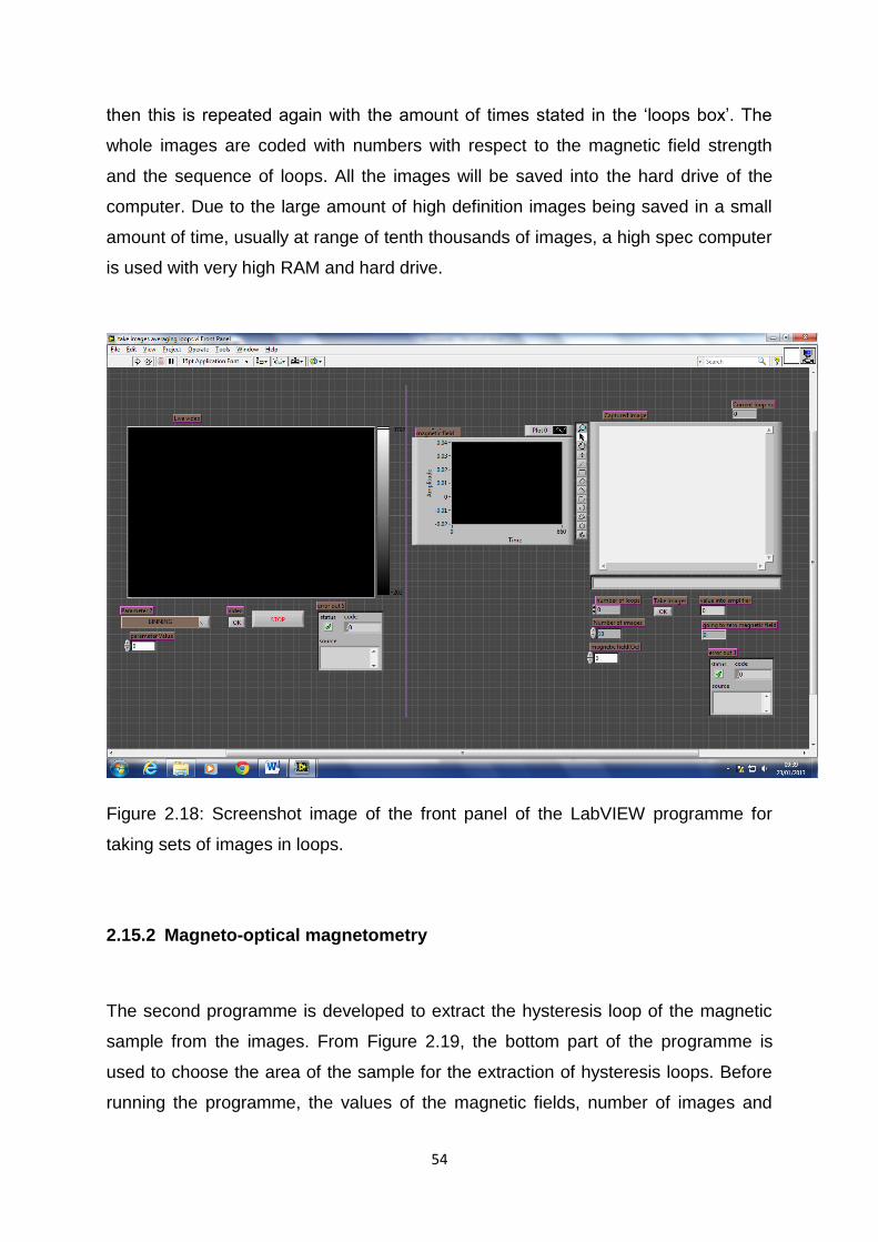
54
then this is repeated again with the amount of times stated in the ‘loops box’. The
whole images are coded with numbers with respect to the magnetic field strength
and the sequence of loops. All the images will be saved into the hard drive of the
computer. Due to the large amount of high definition images being saved in a small
amount of time, usually at range of tenth thousands of images, a high spec computer
is used with very high RAM and hard drive.
Figure 2.18: Screenshot image of the front panel of the LabVIEW programme for
taking sets of images in loops.
2.15.2 Magneto-optical magnetometry
The second programme is developed to extract the hysteresis loop of the magnetic
sample from the images. From Figure 2.19, the bottom part of the programme is
used to choose the area of the sample for the extraction of hysteresis loops. Before
running the programme, the values of the magnetic fields, number of images and

55
loops number must be inserted in the respective box shown on Figure 2.19. These
are the same values that were inserted when taking the pictures. After clicking the
run button, the user will be asked about the location of the folder where the images
were saved in and then the user will be requested to choose the area of the sample
for hysteresis loop extraction as shown in the screenshot of Figure 2.20. The single
hysteresis loop is shown in the right side of the programme as shown in Figure 2.19.
On Figure 2.19 the graph in the middle of the programme shows the time-wave
graph the Kerr signal from a cycle of one loop. The main purpose is to see how large
is the fluctuations of the light source, the electronic drift and other noises. Fluctuation
from the light source and the camera are represented by the formation of slope (not
the high jump caused by magnetisation reversal) in the time wave graph of the Kerr
signal. The final value for every single loop is saved in a folder and will be averaged
by the top part of the programme shown on Figure 2.21.
Figure 2.19: Screenshot of the frontpanel at the bottom part of the LabVIEW for the
hysteresis loops extraction at different part of the sample.

56
Figure 2.20: Screenshot picture when choosing the area of the sample for hysteresis
loop observation. The small green square represents the desired area for hysteresis
loop examination.
The top part of the LabVIEW is for the loop averaging in which it reads the values in
the saved file and then averages them. The averaged hysteresis loop is shown in the
graph at the centre of the front panel shown in screenshot of Figure 2.21. The user
can easily improve the result by using the functions built in the programme. The
functions include slope correction, changing values of averaging point and
normalisation. User can change the values in these functions panel and view the
improvement. A limitless trial can be done to improve the result until the desired
result is achieved. Normalisation is mandatory when doing experiment in which the
repetition is high. It is because of the electronic ‘drift’ when the experiment is running
for a long time causes large difference in the light intensity values for different loops
making it impossible to average them. Therefore, normalisation helps to put all the
hysteresis loops to be in range with each other for averaging. The 2d arrays on the
right side of Figure 2.21 show the coded number of image with respect to the
magnetic field strength. This is very important as a reference of the magnetic field
strength when doing the magnetic domains extraction from the image at different
magnetic field strength and will be described in the next section.
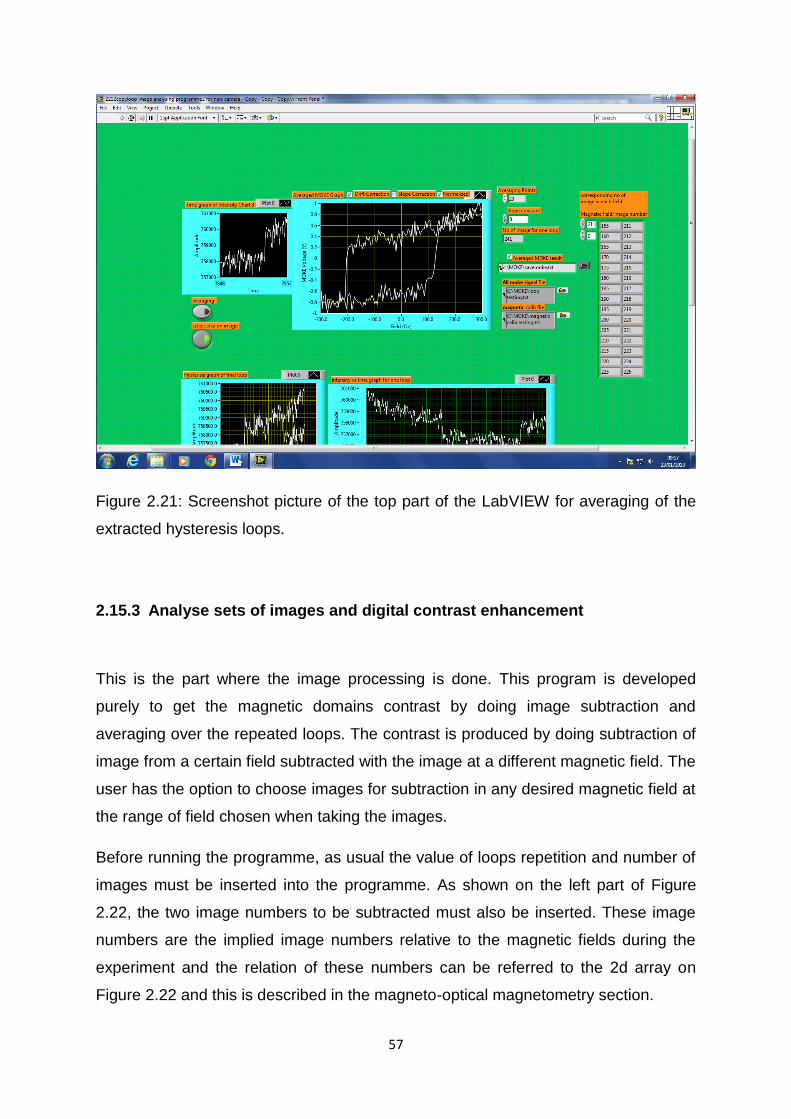
57
Figure 2.21: Screenshot picture of the top part of the LabVIEW for averaging of the
extracted hysteresis loops.
2.15.3 Analyse sets of images and digital contrast enhancement
This is the part where the image processing is done. This program is developed
purely to get the magnetic domains contrast by doing image subtraction and
averaging over the repeated loops. The contrast is produced by doing subtraction of
image from a certain field subtracted with the image at a different magnetic field. The
user has the option to choose images for subtraction in any desired magnetic field at
the range of field chosen when taking the images.
Before running the programme, as usual the value of loops repetition and number of
images must be inserted into the programme. As shown on the left part of Figure
2.22, the two image numbers to be subtracted must also be inserted. These image
numbers are the implied image numbers relative to the magnetic fields during the
experiment and the relation of these numbers can be referred to the 2d array on
Figure 2.22 and this is described in the magneto-optical magnetometry section.
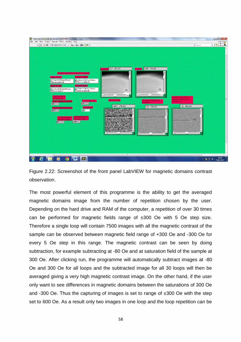
58
Figure 2.22: Screenshot of the front panel LabVIEW for magnetic domains contrast
observation.
The most powerful element of this programme is the ability to get the averaged
magnetic domains image from the number of repetition chosen by the user.
Depending on the hard drive and RAM of the computer, a repetition of over 30 times
can be performed for magnetic fields range of ±300 Oe with 5 Oe step size.
Therefore a single loop will contain 7500 images with all the magnetic contrast of the
sample can be observed between magnetic field range of +300 Oe and -300 Oe for
every 5 Oe step in this range. The magnetic contrast can be seen by doing
subtraction, for example subtracting at -80 Oe and at saturation field of the sample at
300 Oe. After clicking run, the programme will automatically subtract images at -80
Oe and 300 Oe for all loops and the subtracted image for all 30 loops will then be
averaged giving a very high magnetic contrast image. On the other hand, if the user
only want to see differences in magnetic domains between the saturations of 300 Oe
and -300 Oe. Thus the capturing of images is set to range of ±300 Oe with the step
set to 600 Oe. As a result only two images in one loop and the loop repetition can be
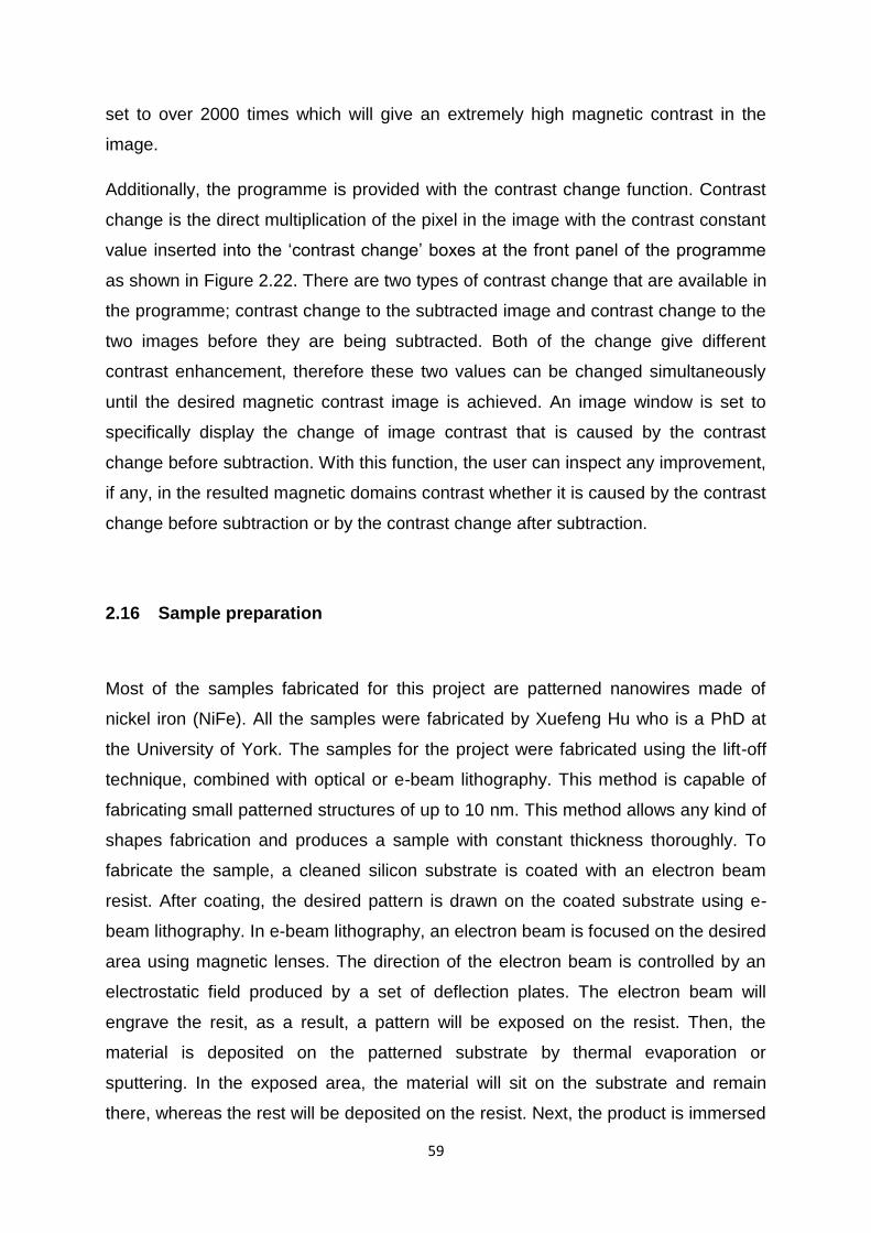
59
set to over 2000 times which will give an extremely high magnetic contrast in the
image.
Additionally, the programme is provided with the contrast change function. Contrast
change is the direct multiplication of the pixel in the image with the contrast constant
value inserted into the ‘contrast change’ boxes at the front panel of the programme
as shown in Figure 2.22. There are two types of contrast change that are available in
the programme; contrast change to the subtracted image and contrast change to the
two images before they are being subtracted. Both of the change give different
contrast enhancement, therefore these two values can be changed simultaneously
until the desired magnetic contrast image is achieved. An image window is set to
specifically display the change of image contrast that is caused by the contrast
change before subtraction. With this function, the user can inspect any improvement,
if any, in the resulted magnetic domains contrast whether it is caused by the contrast
change before subtraction or by the contrast change after subtraction.
2.16 Sample preparation
Most of the samples fabricated for this project are patterned nanowires made of
nickel iron (NiFe). All the samples were fabricated by Xuefeng Hu who is a PhD at
the University of York. The samples for the project were fabricated using the lift-off
technique, combined with optical or e-beam lithography. This method is capable of
fabricating small patterned structures of up to 10 nm. This method allows any kind of
shapes fabrication and produces a sample with constant thickness thoroughly. To
fabricate the sample, a cleaned silicon substrate is coated with an electron beam
resist. After coating, the desired pattern is drawn on the coated substrate using e-
beam lithography. In e-beam lithography, an electron beam is focused on the desired
area using magnetic lenses. The direction of the electron beam is controlled by an
electrostatic field produced by a set of deflection plates. The electron beam will
engrave the resit, as a result, a pattern will be exposed on the resist. Then, the
material is deposited on the patterned substrate by thermal evaporation or
sputtering. In the exposed area, the material will sit on the substrate and remain
there, whereas the rest will be deposited on the resist. Next, the product is immersed
60
in acetone to remove the resists. Therefore only the material on the substrate stays.
This process is called the lift-off. The quality of the deposited material is determined
by the thermal evaporation or the sputtering process but other than that, it is a very
flexible and useful technique for nano-scale pattern fabrication. A summary of this
technique is explained using diagrams shown in Figure 2.23.
Figure 2.23: Summary diagrams of the lift-off technique, combined with optical or e-
beam lithography technique for sample fabrication.
2.17 OOMMF Simulation
The simulation result was done also by Xuefeng Hu who is a Phd student at the
University of York. To do the micromagnetic calculation and simulation, he used
software known as Object Oriented Micro-Magnetics Framework (OOMMF) package.
OOMMF is an open source software which was developed by M. J. Donahue and D.
G. Porter from National Institute of Standards and Technology (NIST) [53].
For the field driven-dynamic magnetisation, the simulations use the Landau-Lifshitz-
Gilbert (LLG) differential equation [54]:
Equation 2.22
where is the LLG gyromagnetic ratio derived as:

61
Equation 2.23
and is the magnetization vector (A/m) per unit, is the effective field vector
(A/m) which depend on energy of system at Equation 2.24, is the damping
coefficient and is the saturation magnetization (A/m), is the Landé factor, is
the charge of electron and is the mass of electron.
Total energy of the system is:
Equation 2.24
The exchange energy is:
Equation 2.25
where is the exchange stiffness, and the anisotropy energy is:
,
Equation 2.26
where is the angle between the direction of magnetization and the symmetric axis.
The demagnetisation energy is:
Equation 2.27
where is the demagnetisation field vector, is the unit vector normal to the
surface and is the relative displacement.
The Zeeman energy is:
Equation 2.28
The effective field is:
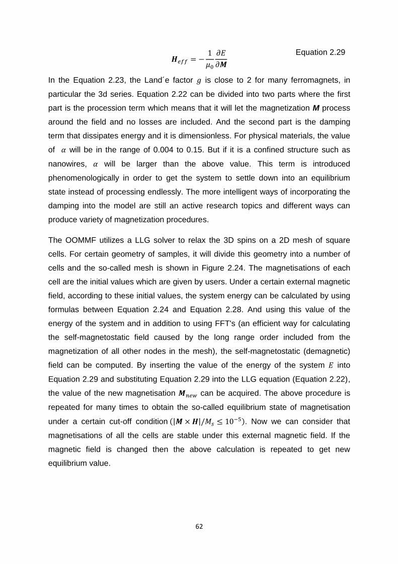
62
Equation 2.29
In the Equation 2.23, the Land´e factor is close to 2 for many ferromagnets, in
particular the 3d series. Equation 2.22 can be divided into two parts where the first
part is the procession term which means that it will let the magnetization M process
around the field and no losses are included. And the second part is the damping
term that dissipates energy and it is dimensionless. For physical materials, the value
of will be in the range of 0.004 to 0.15. But if it is a confined structure such as
nanowires, will be larger than the above value. This term is introduced
phenomenologically in order to get the system to settle down into an equilibrium
state instead of processing endlessly. The more intelligent ways of incorporating the
damping into the model are still an active research topics and different ways can
produce variety of magnetization procedures.
The OOMMF utilizes a LLG solver to relax the 3D spins on a 2D mesh of square
cells. For certain geometry of samples, it will divide this geometry into a number of
cells and the so-called mesh is shown in Figure 2.24. The magnetisations of each
cell are the initial values which are given by users. Under a certain external magnetic
field, according to these initial values, the system energy can be calculated by using
formulas between Equation 2.24 and Equation 2.28. And using this value of the
energy of the system and in addition to using FFT's (an efficient way for calculating
the self-magnetostatic field caused by the long range order included from the
magnetization of all other nodes in the mesh), the self-magnetostatic (demagnetic)
field can be computed. By inserting the value of the energy of the system into
Equation 2.29 and substituting Equation 2.29 into the LLG equation (Equation 2.22),
the value of the new magnetisation can be acquired. The above procedure is
repeated for many times to obtain the so-called equilibrium state of magnetisation
under a certain cut-off condition . Now we can consider that
magnetisations of all the cells are stable under this external magnetic field. If the
magnetic field is changed then the above calculation is repeated to get new
equilibrium value.

63
Figure 2.24: Mesh of simulation points for an elliptical sample.
Finally, there are key points to take into consideration:
(1) The cell size is very important to choose before performing simulation. Generally
speaking, it should be smaller or close to the exchange length of the material. This is
mentioned in section 1.6.
(2) The lateral condition of the geometry of the sample will affect the simulation. The
cell shape chosen for the simulation is cube shape. Therefore if non regular shape
such as circle, the simulation will produce wrong simulation results..
(3) Damping parameter is crucial that affect the simulation. If it is too small, the
whole simulation will takes a very long time. Therefore choosing a value of around
0.5 will accelerate the calculation speed and simulated result will not be largely
deviated from the actual process (real situation).
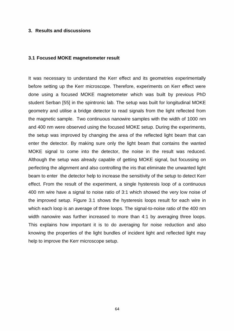
64
3. Results and discussions
3.1 Focused MOKE magnetometer result
It was necessary to understand the Kerr effect and its geometries experimentally
before setting up the Kerr microscope. Therefore, experiments on Kerr effect were
done using a focused MOKE magnetometer which was built by previous PhD
student Serban [55] in the spintronic lab. The setup was built for longitudinal MOKE
geometry and utilise a bridge detector to read signals from the light reflected from
the magnetic sample. Two continuous nanowire samples with the width of 1000 nm
and 400 nm were observed using the focused MOKE setup. During the experiments,
the setup was improved by changing the area of the reflected light beam that can
enter the detector. By making sure only the light beam that contains the wanted
MOKE signal to come into the detector, the noise in the result was reduced.
Although the setup was already capable of getting MOKE signal, but focussing on
perfecting the alignment and also controlling the iris that eliminate the unwanted light
beam to enter the detector help to increase the sensitivity of the setup to detect Kerr
effect. From the result of the experiment, a single hysteresis loop of a continuous
400 nm wire have a signal to noise ratio of 3:1 which showed the very low noise of
the improved setup. Figure 3.1 shows the hysteresis loops result for each wire in
which each loop is an average of three loops. The signal-to-noise ratio of the 400 nm
width nanowire was further increased to more than 4:1 by averaging three loops.
This explains how important it is to do averaging for noise reduction and also
knowing the properties of the light bundles of incident light and reflected light may
help to improve the Kerr microscope setup.
65
Figure 3.1: Hysteresis loops result from 1000 nm and 400 nm width nanowires using
focused MOKE magnetometer. Each hysteresis loop is an average of 3 loops.
3.2 Result from nickel iron (Ni80Fe20) thin film
A NiFe thin film sample was used to test the Kerr microscope setup before doing
experiments on nanostructures samples. This helps to confirm whether the setup is
able to detect the Kerr effect or not. The microscope was set to longitudinal
sensitivity mode and the thin film sample was oriented such that its easy axis is
parallel to the longitudinal MOKE axis of the setup. As described before, ‘mode’
control was done by placing the aperture stop of the aperture diaphragm at the right
position and this is explained in the experimental techniques part of this thesis.
Given in Figure 3.2 is the result of single shot hysteresis loops of the thin film at
different sizes of chosen area. It was explained in the experimental techniques
chapter that the user is capable of choosing any area of any size in the field of view
of the microscope for the extraction of hysteresis loop in the sample. From Figure
3.2, it clearly shows that increasing the region of interest (ROI) will increase the
value of the detected Kerr signal. As predicted, larger area of samples will gives
higher Kerr effect signal. In conclusion, results in Figure 3.2 confirm that the Kerr
microscope is working well as well as capable of getting MOKE signal of up to an
area of size 1x1 µm and smaller. The result is a single hysteresis loop data, by doing
repetition and averaging of loops will help to improve the weak Kerr signal from
Magnetic field (Oe) Magnetic field (Oe)
1000 nm width wire 400 nm width wire

66
nanowires.
2
Magnetic field(Oe)
-250 -200 -150 -100 -50 0 50 100 150 200 250 300
-1.0
-0.5
0.0
0.5
1.01
Magnetic field(Oe)
-250 -200 -150 -100 -50 0 50 100 150 200 250 300
Inte
nsity (
arb
. units)
-1.0
-0.5
0.0
0.5
1.0
ROI=5x5µm ROI=1x1µm
Figure 3.2: Single hysteresis loop at different size of region of interest (ROI).
3.3 Nanowires results
This project focused on the magnetic characteristic of nano-samples. All the samples
were fabricated by Xuefeng Hu, the samples are Ni80Fe20 with the thickness of 20
nm. Before doing experiment on any of the nano-samples, it was first saturated with
a +1000 Oe magnetic field and return back to 0 Oe. For all the nano-samples
investigated in this project, the experiments were cycled 20 times to produce
average of hysteresis loops with the magnetic field ‘step’ to be 5 Oe. It was found
that these values are the optimum working condition of the whole setup in relation to
the computer capability. The repetition also helps to enhance the magnetic domains
contrast in the static images of the samples which is also examined in this project.
When doing the extraction for hysteresis loops in different areas of the sample, the
selected area size is always set to around less than 1 µm x 1 µm to easily generalise
the magnetic property in each area without having to compare the different sizes
effect of the examined regions. Furthermore, the known effective smallest size of
focused MOKE laser point is at 1 µm diameter [56, 57], thus this gives an additional
advantage for this Kerr microscopy technique for the possibility of hysteresis loop
observation for an area smaller than 1µm width. This is especially useful when
examining micro size samples with multiple magnetic domains with width smaller
than 1 µm. For all the samples a positive magnetic field is to the right direction and a
negative magnetic field aligned in the left direction.
Magnetic field (Oe) Magnetic field (Oe)

67
3.4 Cross-wire sample
The first nanowire sample is a cross-shaped nanowire with width of around 1 µm.
The experiment was done with the longitudinal Kerr sensitivity setup mode with the
longitudinal axis shown in Figure 3.3. The regions of interest for hysteresis loops
extractions are shown in Figure 3.3 and will further be discussed using the magnetic
domains image results. From the hysteresis loops in Figure 3.4, the coercivity values
at different parts of the nanowire are different, suggesting that there are magnetic
domains formed at single arm of the wire before the wire is saturated. This is
because, when only some parts of the wire has their magnetisation reversed by the
external field, the parts that have not been reversed will have opposite magnetisation
direction with the reversed parts. Therefore magnetic domains formed at different
magnetisation directions. By referring to the hysteresis loop results in Figure 3.4,
areas in parts 1 and 8 have the coercivities of 101±4 Oe and 108±4 Oe respectively
where these are the two highest coercivity values, therefore magnetisation in these
areas will be reversed at higher applied magnetic field than the other.
Figure 3.3: Scanning electron microscopy (SEM) image of the cross nanowire with
the plane of incident and applied field direction H shown in the figure. The numbered
areas represent the areas of interest for hysteresis loops extraction.

68
5
Magnetic field(Oe)
-200 -150 -100 -50 0 50 100 150 200
Inte
nsity (
arb
. units)
-1.0
-0.5
0.0
0.5
1.06
Magnetic field(Oe)
-200 -150 -100 -50 0 50 100 150 200
Inte
nsity
(arb
. units
)
-1.0
-0.5
0.0
0.5
1.0
7
Magnetic field(Oe)
-200 -150 -100 -50 0 50 100 150 200
-1.0
-0.5
0.0
0.5
1.08
Magnetic field(Oe)
-200 -150 -100 -50 0 50 100 150 200
-1.0
-0.5
0.0
0.5
1.0
3
-200 -150 -100 -50 0 50 100 150 200
Inte
nsity (
arb
. units)
-1.0
-0.5
0.0
0.5
1.0
2
-200 -150 -100 -50 0 50 100 150 200
Inte
ns
ity
(arb
. u
nits
)
-1.0
-0.5
0.0
0.5
1.01
-200 -150 -100 -50 0 50 100 150 200
Inte
nsity (
arb
. units)
-1.0
-0.5
0.0
0.5
1.0
Hc=78 OeH
c=101 Oe
Hc=75 Oe
Hc=85 Oe
Hc=80 Oe
Hc=93Oe
Hc=108 Oe
4
-200 -150 -100 -50 0 50 100 150 200
-1.0
-0.5
0.0
0.5
1.0
Hc=77 Oe
Figure 3.4: Hysteresis loop results of the cross wire at different regions with the
coercivity values displayed for each parts. The numbers represent ROI (region of
interest) corresponding to the numbered areas in Figure 3.3.
Because of the magnetostatic energy and the shape anisotropy effects, the magnetic
moment spins in the cross wire will aligned along the edges for lower energy. For
Magnetic field (Oe) Magnetic field (Oe)

69
example, lowest energy for vertical wire will be at vertical direction along the edges
and vice versa. From the hysteresis loop results in Figure 3.4, all area except the
centre (part 4) are easy axis loops which suggest that the easy axis of the
magnetisation is along the wire edges. The hysteresis loop from part 4 is an inter-
media axis loop which suggests that there is a vortex domain formed at the line
orientation at the junction. The same result was observed by Yongbing [58] and at
[59] where vortex domain was observed at the cross wire junction.
10
Magnetic field(Oe)
-250 -200 -150 -100 -50 0 50 100 150 200 250
-1.0
-0.5
0.0
0.5
1.09
Magnetic field(Oe)
-250 -200 -150 -100 -50 0 50 100 150 200 250
Inte
nsity (
arb
. units)
-1.0
-0.5
0.0
0.5
1.0
Figure 3.5: Hysteresis loops of the transverse magnetisations in the vertical arms of
the cross wire. Shape of loops explains the magnetisation saturation along the hard
axis (vertical) of the sample.
The vertical arms in the cross sample have transverse Kerr sensitivity because the
magnetisation direction (vertical axis) is perpendicular to the plane of light incidence.
Although the setup is for longitudinal Kerr effect, there is still transverse effect in the
image as transverse Kerr effect causes change to the light intensity and is not
affected by the presence of an analyser. The transverse Kerr effect results of area 9
and 10 (refer to Figure 3.3) are shown in Figure 3.5 and the hysteresis loops show
the saturation of the wire along its hard axis.
Magnetic field (Oe) Magnetic field (Oe)

70
Figure 3.6: Magnetic domain images of the cross wire at different magnetic fields.
These are the final results after the magnetic images are produced through image
subtraction and image processing as explained in the experimental method section.
The SEM image (top) of the sample is numbered at the ROIs. Dark contrast
represents magnetisation reversal by applied magnetic field.
In the magnetic domains images in Figure 3.6, the dark contrast shows magnetic
reversal and the light contrast represents the magnetic moment at parts which is not
yet reversed by the applied magnetic field. From picture A in Figure 3.6, the
magnetic domains image for the cross wire indicates that there is a formation of
magnetic domains just before the wire is fully saturated. This confirms with the
results from the hysteresis loops Figure 3.4 as explained before and the domain
F
C
B
D
A
E
-77 Oe
-81 Oe
-85 Oe
-89 Oe
-93 Oe
-108 Oe
SEM image of the cross wire
with the numbered ROIs.
Dark contrast
White contrast

71
walls motion can be seen in the images, though the structure of the domain wall is
too small to be seen due to the resolution limit of the microscope. The same pattern
of magnetic domains formation is discovered in the experiments both when the
applied magnetic fields are in the positive and negative directions. This pattern is
shown in Figure 3.6 in steps of different magnetic fields. For simplicity, magnetisation
reversal pattern in the negative magnetic field will be discussed. From Figure 3.4,
parts 2, 4, 5 and 7 have negative magnetic field coercivities of -81±4 Oe, -82±4 Oe, -
77±4 Oe and -85±4 Oe respectively and referring to image A in Figure 3.6, it is
shown that these areas are the first four areas to experience magnetisation reversal
by applied magnetic field of -77 Oe. The coercivities for areas 1, 6 and 8 are around
-105±4 Oe,-94 ±4 Oe and -107±4 Oe and it is shown that the spin in these areas are
not yet reversed by applied magnetic field at -89±4 Oe (shown in image D Figure
3.6). Not until at -93±4 Oe (image E) where these area starts to reverse and finally at
-108±4 Oe (image F) they are all saturated. This unique effect in the cross-shaped
nanowire is caused by the ferromagnetic characteristics of the wire.
3.5 Zigzag nanowire
The next sample is a zigzag nanowire with width of around 841 nm. The geometry of
the zigzag nanowire is shown in Figure 3.7 together with its width and length values.
Directly referring to the hysteresis loops results in Figure 3.9 a hard to generalise
loops patterns are observed. The coercivities in the positive and negative fields in
each loops are different. This is the characteristic of the ferromagnetic zigzag
nanowire for the reason that is related to the domain walls motion formed at the
corners of the zigzag nanowire. The patterns can be easily studied by referring to the
magnetic images results in Figure 3.9. The ROIs are also shown in Figure 3.9 and
the magnetisation and the Kerr effects from different MOKE geometry is shown in
Figure 3.8.

72
Figure 3.7: SEM image of the zigzag nanowire.
Figure 3.8: Zigzag nanowire Longitudinal and transverse MOKE geometry with the
direction of the applied magnetic field and plane of incident light as shown above.

73
4
Magnetic field(Oe)
-200 -150 -100 -50 0 50 100 150 200
Inte
nsity
(arb
. units
)
-1.0
-0.5
0.0
0.5
1.0
6
Magnetic field(Oe)
-200 -150 -100 -50 0 50 100 150 200
Inte
nsity (
arb
. units)
-1.0
-0.5
0.0
0.5
1.0
7
Magnetic field(Oe)
-200 -150 -100 -50 0 50 100 150 200
Inte
nsity (
arb
. units)
-1.0
-0.5
0.0
0.5
1.0
5
-200 -150 -100 -50 0 50 100 150 200
Inte
ns
ity
(arb
. u
nits
)
-1.0
-0.5
0.0
0.5
1.0
3
-200 -150 -100 -50 0 50 100 150 200
Inte
ns
ity
(arb
. u
nits
)
-1.0
-0.5
0.0
0.5
1.0
1
-200 -150 -100 -50 0 50 100 150 200
Inte
nsity (
arb
. units)
-1.0
-0.5
0.0
0.5
1.02
-200 -150 -100 -50 0 50 100 150 200
Inte
nsity (
arb
. units)
-1.0
-0.5
0.0
0.5
1.0
-Hc= -82 Oe
-Hc= -73 Oe
-Hc= -93 Oe
-Hc= -78Oe
-Hc= -85 Oe-H
c= -77 Oe
-Hc=-82 Oe
Hc=49 Oe H
c=49 Oe
Hc=77 Oe
Hc=52 Oe
Hc=53 Oe
Hc=66 Oe
Hc= 68 Oe
Figure 3.9: The hysteresis loops value of the zigzag nanowire (bottom) and the
region of interests (ROIs) areas (top).
Magnetic field (Oe)
Magnetic field (Oe)
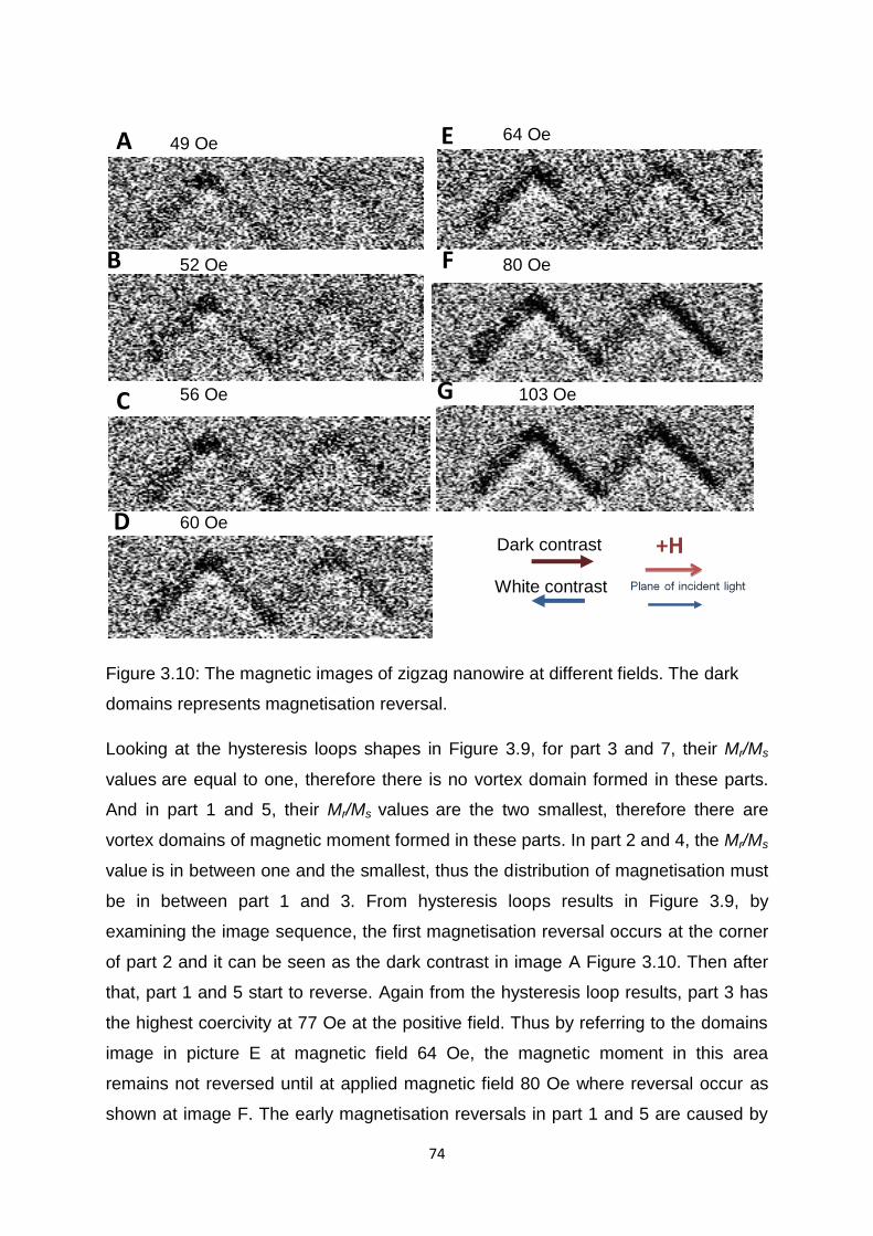
74
Figure 3.10: The magnetic images of zigzag nanowire at different fields. The dark
domains represents magnetisation reversal.
Looking at the hysteresis loops shapes in Figure 3.9, for part 3 and 7, their Mr/Ms
values are equal to one, therefore there is no vortex domain formed in these parts.
And in part 1 and 5, their Mr/Ms values are the two smallest, therefore there are
vortex domains of magnetic moment formed in these parts. In part 2 and 4, the Mr/Ms
value is in between one and the smallest, thus the distribution of magnetisation must
be in between part 1 and 3. From hysteresis loops results in Figure 3.9, by
examining the image sequence, the first magnetisation reversal occurs at the corner
of part 2 and it can be seen as the dark contrast in image A Figure 3.10. Then after
that, part 1 and 5 start to reverse. Again from the hysteresis loop results, part 3 has
the highest coercivity at 77 Oe at the positive field. Thus by referring to the domains
image in picture E at magnetic field 64 Oe, the magnetic moment in this area
remains not reversed until at applied magnetic field 80 Oe where reversal occur as
shown at image F. The early magnetisation reversals in part 1 and 5 are caused by
B
A
D
C
F
E
G
56 Oe
52 Oe
49 Oe
60 Oe
64 Oe
80 Oe
103 Oe
Dark contrast
White contrast

75
the domain walls motion that formed earlier at the corners of the sample. These
walls will move driven by the magnetic field to cause early magnetisation reversal
than usual. Additionally in part 1, the end of the arm has a shape anisotropy effect
where the magnetic moments tend to align along the edge, therefore there is
magnetic domain formed due to this effect that also contribute to the magnetisation
distribution in that area. In image E Figure 3.10, it is shown that the domain wall
separating domains in part 2 and part 3 moves to the right side at magnetic field of
64 Oe. The results display the complicated distributions of magnetisation in zigzag
nanowire which was caused by the magnetostatic effect and the domain walls
motion. Same patterns are also observed in the positive magnetic field experiment
and thus, confirming the ferromagnetic properties of the zigzag nanowires. It is
observed that the coercivity values at opposite applied magnetic fields are different
in zigzag nanowire. The differences in the coercivity values between the negative
and positive magnetic fields are shown in Table 3.1.
Area
no. -Hc (Oe) Hc (Oe)
Coercivites
difference
(Oe)
1 78 49 29
2 73 49 24
3 93 77 16
4 82 52 30
5 77 53 24
6 85 66 19
Table 3.1: Table showing the difference in coercivities between the positive and
negative field.
The transverse Kerr effect in the zigzag nanowire gives different transverse
directions in each arm, this is summarised in diagram form in Figure 3.8. For that
reason, a distinct black and white contrasts will form in each arm describing the
opposite magnetisation direction of transverse Kerr effect. To observe this effect, the
Kerr microscope setup was changed into the transverse MOKE sensitivity by means
of longitudinal to transverse sensitivity setup. This method change the transverse
Kerr effect into longitudinal Kerr effect as described in the experimental section of

76
this thesis and thus will effectively observe the transverse Kerr effect. The resulting
magnetic domains in the zigzag nanowire are shown in Figure 3.12. Black and white
contrasts formed in the image in Figure 3.12. It means that the magnetisation
direction of white and black contrast is opposite to each other. Because the
measurement is a transverse Kerr effect, opposite ‘jumps’ of the hysteresis loops in
arms 1 and 4 are observed shown in Figure 3.11. Therefore, this strongly supports
the transverse Kerr effect discussion above. The results not just verify the transverse
Kerr effect in the zigzag nanowire but in addition to that, they also demonstrate the
working ability of the Kerr microscope to detect the transverse Kerr effect by using
the longitudinal with transverse sensitivity setup.
1
Magnetic field(Oe)
-250 -200 -150 -100 -50 0 50 100 150 200 250
Inte
nsity (
arb
. units)
-1.0
-0.5
0.0
0.5
1.0
3
Magnetic field(Oe)
-250 -200 -150 -100 -50 0 50 100 150 200 250
-1.0
-0.5
0.0
0.5
1.0
-Hc=-177 Oe
2
Magnetic field(Oe)
-250 -200 -150 -100 -50 0 50 100 150 200 250
Inte
nsity
(arb
. units)
-1.0
-0.5
0.0
0.5
1.04
Magnetic field(Oe)
-250 -200 -150 -100 -50 0 50 100 150 200 250
-1.0
-0.5
0.0
0.5
1.0
Figure 3.11: Hysteresis loops of zigzag nanowire for the transverse geometry but by
using longitudinal with transverse sensitivity setup.
Magnetic field (Oe) Magnetic field (Oe)
Magnetic field (Oe) Magnetic field (Oe)
+H Plane of
incident light

77
Figure 3.12: Transverse MOKE image of the nanowire showing black and white
pattern.
3.6 Nanowires with asymmetric notch and nucleation pad
Due to the effect of shape anisotropy on the alignment of magnetic spins in the
sample, the pad will has lower coercivity because the magnetic spin in the pad form
a vortex along the circular edge of the pad. Because of this fact, there is a domain
wall at the junction between the nanowire and the pad separating the magnetic
domains in each area. This domain wall can be propagated along the wire driven by
the magnetic field to cause an early magnetisation reversal along the wire. But the
introduction of notch will pin the domain wall to cause different distribution of
magnetisation direction in the nanowires.
A set of samples was prepared for the magnetic domains observation in nanowires
with asymmetric notch. For all the samples, their asymmetric notches are fabricated
to have one short side and one long side. Measuring from the long axis of each wire,
the short side have angle of between 12ᵒ and 15ᵒ, whereas the long side have angle
of between 42ᵒ and 55ᵒ. All the short side of the notches are facing the nucleation
pad of the nanowire. The samples can be generalised into two categories, the first
group is for samples with their notches located in the middle of the nanowire and the
second group is for samples with their notches positioned at about a quarter length
of the wire away from the nucleation pad. Their dimensions are described in Table
3.2.
+H
Plane of
incident light
Dark contrast
White contrast

78
Group
Sample
number
Width
of wire
(nm)
Notch
depth
(nm)
Percentage of notch depth to the width
of wire (%)
1 4 321 92 28.7
11 324 131 40.4
2 7 384 152 39.6
6 435 202 46.4
5 334 111 33.2
14 394 223 56.6
13 374 192 51.3
12 354 172 48.6
Table 3.2: Table showing the geometry of the wires with notch.
In the first group, there are two wires with nearly the same width but different notch
depth. The experiments were done using the usual longitudinal Kerr sensitivity setup
where the magnetisation direction is parallel to the plane of incidence.

79
3.6.1 Group one
Sample 11
Graph 1
Magnetic field(Oe)
-250 -200 -150 -100 -50 0 50 100 150 200 250
Inte
nsity (
arb
. units)
-1.0
-0.5
0.0
0.5
1.0 Graph 2
Magnetic field(Oe)
-250 -200 -150 -100 -50 0 50 100 150 200 250
-1.0
-0.5
0.0
0.5
1.0
Graph 3
Magnetic field(Oe)
-250 -200 -150 -100 -50 0 50 100 150 200 250
Inte
nsity (
arb
. units)
-1.0
-0.5
0.0
0.5
1.0
Graph 4
Magnetic field(Oe)
-250 -200 -150 -100 -50 0 50 100 150 200 250
-1.0
-0.5
0.0
0.5
1.0
Graph 5
Magnetic field(Oe)
-250 -200 -150 -100 -50 0 50 100 150 200 250
Inte
nsity (
arb
. units)
-1.0
-0.5
0.0
0.5
1.0 Graph 6
Magnetic field(Oe)
-250 -200 -150 -100 -50 0 50 100 150 200 250
-1.0
-0.5
0.0
0.5
1.0
Graph 7
Magnetic field(Oe)
-250 -200 -150 -100 -50 0 50 100 150 200 250
Inte
nsity (
arb
. units)
-1.0
-0.5
0.0
0.5
1.0
-Hc=-148 Oe
-Hc=-196 Oe
Hc=185 Oe
-Hc=-147 Oe
-Hc=-145 Oe
-Hc=-117Oe
-Hc=-141 Oe
-Hc=-79 Oe
-Hc=-128 Oe
Hc=129 Oe
Hc=123 Oe
Hc=104 Oe
Hc=122 Oe
Hc=64 Oe
Figure 3.13: SEM image (top) of sample 11 with the numbered ROIs. Hysteresis
loops (bottom) result of sample 11 corresponding to the area shown at the nanowire.
Magnetic field (Oe)
Magnetic field (Oe)

80
Sample 11 has wire width of 324 nm and notch depth of around 131 nm. The
hysteresis loop results at different parts of the wire are shown in Figure 3.13 and
magnetic domain images of the sample are shown in Figure 3.14. There is a
dominant grey region in the pad of the sample at all magnetic fields and can be seen
in the domain images in picture F in Figure 3.14. This is not a magnetic contrast in
the sample and is caused by the saturated pixels in that area. The main reason is
because the light intensity and exposure time for the camera was set to optimum
only for the nanowire part. As a result, the large pad size is too bright and causes
saturation to the pixels. Though, it still contains some Kerr signal which is proven by
the hysteresis loop at part 7 of Figure 3.13. In general, the propagation of domain
wall in both negative and positive applied magnetic field are the same, but for this
sample the discussion will focus on magnetic domain wall formed at negative applied
magnetic field. As discussed before, the elliptical pad has the lowest coercivity
compared to the other parts of the nanowire. From graph 6 in Figure 3.13, it is
indicated that the domain wall started to propagate to the wire at magnetic field
strength of -117 Oe (negative field coercivity). This propagation is shown in the
magnetic image A in Figure 3.14 for which the magnetisation in part 6 has started to
reverse. Again from Figure 3.13, regions in part 2, 3 and 4 have nearly the same
coercivity values. As a result, the magnetisation reversals in these regions are nearly
at the same time and this is pictured in the magnetisation reversal at image B and C
of Figure 3.14. The end of the nanowire at part 1 have the highest coercivity and its
magnetisation is not yet reversed at negative field of -151 Oe which is presented in
picture C of Figure 3.14. However the magnetisation is reversed at coercivity value
of -196 Oe as shown in the hysteresis loop result (Figure 3.13) and the image after
reversal can be seen at picture E in Figure 3.14. At the range of -196 Oe the domain
wall in the nanowire disappear because in the whole region of the nanowire, the
magnetisation is aligned in the same direction along the long axis of the nanowire.
Finally, it can be seen that the difference of coercivity values between part 2 and 5 is
only around 7 Oe for both negative magnetic field and positive magnetic field which
means that the pinning of domain wall propagation affected by the notch structure is
very weak as the coercivity values difference is too small.

81
Figure 3.14: SEM image (top) of sample 11 with the numbered ROIs. Magnetic
domain images (bottom) of sample 11, dark contrast corresponds to reversed
magnetisation by the applied magnetic field.
F
D
C
G
J E
B
A
I
H
Dark contrast
White contrast
Dark contrast
White contrast

82
Sample 4
1
Magnetic field(Oe)
-250 -200 -150 -100 -50 0 50 100 150 200 250
Inte
nsity (
arb
. units)
-1.0
-0.5
0.0
0.5
1.0 2
Magnetic field(Oe)
-250 -200 -150 -100 -50 0 50 100 150 200 250
-1.0
-0.5
0.0
0.5
1.0
3
Magnetic field(Oe)
-250 -200 -150 -100 -50 0 50 100 150 200 250
Inte
nsity (
arb
. units)
-1.0
-0.5
0.0
0.5
1.0
4
Magnetic field(Oe)
-250 -200 -150 -100 -50 0 50 100 150 200 250
Inte
nsity (
arb
. units)
-1.0
-0.5
0.0
0.5
1.0
-Hc=-177 Oe
Hc=160 Oe
-Hc=-172 Oe
Hc=160 Oe
-Hc=-160 Oe
Hc=147 Oe
-Hc=-114 Oe
Hc=100 Oe
Figure 3.15: SEM image (top) of sample 4 with the numbered ROIs. Hysteresis loops
(bottom) result of different parts of wire 4.
The wire width of sample 4 is 321 nm and notch depth of around 92 nm. As
demonstrated by the hysteresis loops in Figure 3.15, the same progression occur in
the second sample similar to the progression in sample 11. Again due to pixels
saturation, the pad is covered by strong grey contrast as seen in Figure 3.16. The
image results focus only at the positive magnetic field for generalisation of the
magnetisation distribution in this sample. In this case, for the positive magnetic field
the domain wall produced at the junction between the pad and the wire is a tail-to-tail
domain wall. Domain wall propagation starts at 100 Oe at part 4 as shown by the
coercivity result in graph 4 of Figure 3.15. At 146 Oe, the domain wall remains in the
region around part 4 as shown by the magnetic image in picture A of Figure 3.16.
The difference in coercivity in part 2 and 3 of the wire is 12 Oe and 13 Oe for the
Magnetic field (Oe) Magnetic field (Oe)

83
negative field and positive field respectively. This can be seen in picture b in Figure
3.16 where only half of the wire has its magnetisation reversed and the other half
near the end is not yet reversed.
Figure 3.16: SEM image (top) of sample 4 with the numbered ROIs. Magnetic
domain images (bottom) of sample 4, dark contrast corresponds to reversed
magnetisation by the applied magnetic field. The grey regions in the pad are the
saturated pixels (no Kerr data) of the camera.
3.6.2 Discussion for group one
The results show that the pinning of domain wall causes different magnetisation
distributions in the wire at different magnetic field. Further, the magnetic field driven
depinning of the domain wall at the notch is also observed. It is proven from the
result that the strength of domain wall pinning depends on the percentage depth of
the notch with the wire width. For sample 11 with percentage notch depth of 28.7%,
B
A
C
D
Dark contrast
White contrast

84
it has a coercivity difference between before and after notch at about 6 Oe. And the
difference in coercivity between before and after notch for sample 4 is around 12 Oe.
Thus, the difference is two times larger in sample 4 than in sample 11. This proves
that the deeper the notch is the stronger the pinning effect will be. To produce a
much larger difference in coercivities of area before and after notch, the nucleation
pad for the samples can be modified to a shape that have lower coercivity so that
domain wall can be formed at a much lower magnetic field.
3.6.3 Group two
For group two samples, the magnetic domains formed at the samples when the
magnetisation starts to reverse and before the wire magnetisation is fully saturated.
The patterns are repeatable and formed at both positive applied magnetic field and
negative applied magnetic field. Each sample produces different magnetic domains
pattern and will be describe in detail in this section.

85
Sample 14
1
Magnetic field(Oe)
-250 -200 -150 -100 -50 0 50 100 150 200 250
Inte
nsity (
arb
. units)
-1.0
-0.5
0.0
0.5
1.02
Magnetic field(Oe)
-250 -200 -150 -100 -50 0 50 100 150 200 250
-1.0
-0.5
0.0
0.5
1.0
3
Magnetic field(Oe)
-250 -200 -150 -100 -50 0 50 100 150 200 250
Inte
nsity (
arb
. units)
-1.0
-0.5
0.0
0.5
1.04
Magnetic field(Oe)
-250 -200 -150 -100 -50 0 50 100 150 200 250
-1.0
-0.5
0.0
0.5
1.0
5
-250 -200 -150 -100 -50 0 50 100 150 200 250
Inte
nsity (
arb
. units)
-1.0
-0.5
0.0
0.5
1.0 6
-250 -200 -150 -100 -50 0 50 100 150 200 250
Inte
nsity
(arb
. units
)
-1.0
-0.5
0.0
0.5
1.0
7
-250 -200 -150 -100 -50 0 50 100 150 200 250
Inte
nsity (
arb
. units)
-1.0
-0.5
0.0
0.5
1.08
-300 -200 -100 0 100 200 300
-1.0
-0.5
0.0
0.5
1.0
Hc=134 Oe
-Hc=-140Oe
-Hc=-150 Oe -H
c=-131 Oe
-Hc=-134Oe
-Hc=-127 Oe
-Hc=-135 Oe
-Hc=-65Oe
-Hc=-129 Oe
Hc=115Oe
Hc=117Oe H
c=136 Oe
Hc=120 Oe H
c=124Oe
Hc=117 Oe
Hc=49 Oe
Figure 3.17: Scanning electron microscopy (SEM) image (top) of sample 14 with the
numbered ROIs. Hysteresis loops (bottom) of sample 14 at different parts of the wire.
Magnetic field (Oe) Magnetic field (Oe)

86
The coercivity values shown in Figure 3.17 indicate that there is a multiple magnetic
domains formation in the nanowire during magnetisation reversal. The pattern of the
magnetic domains can be easily explained by referring to the magnetic domain
image results of the nanowire shown in Figure 3.18. The domain wall propagation
from the junction at part 7 can be seen at picture A in Figure 3.18. Before the domain
wall propagate further to the notch, at the same time, region around part 2 undergo
magnetisation reversal as shown in picture B in Figure 3.18 and it is confirmed by
the hysteresis loop result shown in Figure 3.17. This is unexpected as such pattern
was never been observed before [60, 61, 62]. The two domain walls in part 2
propagate sideways until all the magnetisation in the whole wire gets reversed. The
whole events can be seen in details by the magnetic domains image in Figure 3.18.
Figure 3.18: SEM image of sample 14 (top). Magnetic domain images (bottom) of
sample 14 where the dark domain contrast represents magnetisation reversal.
B
A
F
C
E
D
G
I
H
L
K
J
+H Dark contrast White contrast
Dark contrast
White contrast Plane of light incident
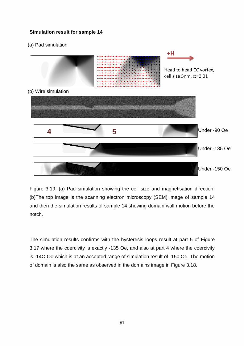
87
Simulation result for sample 14
Figure 3.19: (a) Pad simulation showing the cell size and magnetisation direction.
(b)The top image is the scanning electron microscopy (SEM) image of sample 14
and then the simulation results of sample 14 showing domain wall motion before the
notch.
The simulation results confirms with the hysteresis loops result at part 5 of Figure
3.17 where the coercivity is exactly -135 Oe, and also at part 4 where the coercivity
is -14O Oe which is at an accepted range of simulation result of -150 Oe. The motion
of domain is also the same as observed in the domains image in Figure 3.18.
Under 150Oe
(a) Pad simulation
(b) Wire simulation
Under -90 Oe
Under -135 Oe
Under -150 Oe
4 5
+H

88
Sample 13
1
Magnetic field(Oe)
-250 -200 -150 -100 -50 0 50 100 150 200
Inte
nsity (
arb
. units)
-1.0
-0.5
0.0
0.5
1.02
Magnetic field(Oe)
-250 -200 -150 -100 -50 0 50 100 150 200
-1.0
-0.5
0.0
0.5
1.0
3
Magnetic field(Oe)
-250 -200 -150 -100 -50 0 50 100 150 200
Inte
nsity (
arb
. units)
-1.0
-0.5
0.0
0.5
1.04
Magnetic field(Oe)
-250 -200 -150 -100 -50 0 50 100 150 200
-1.0
-0.5
0.0
0.5
1.0
5
-250 -200 -150 -100 -50 0 50 100 150 200
Inte
nsity (
arb
. units)
-1.0
-0.5
0.0
0.5
1.0 6
-250 -200 -150 -100 -50 0 50 100 150 200
-1.0
-0.5
0.0
0.5
1.0
7
-250 -200 -150 -100 -50 0 50 100 150 200 250
Inte
nsity (
arb
. units)
-1.0
-0.5
0.0
0.5
1.08
-300 -200 -100 0 100 200 300
-1.0
-0.5
0.0
0.5
1.0
Hc=128 Oe
-Hc=-137Oe
-Hc=-136 Oe
-Hc=-134 Oe
-Hc=-149Oe
-Hc=-137 Oe
-Hc=-144 Oe
-Hc=-84Oe-H
c=-154Oe
Hc=123Oe
Hc=125Oe H
c=124 Oe
Hc=144 Oe
Hc=140Oe
Hc=141 Oe
Hc=57 Oe
Figure 3.20: SEM image of sample 13 (top) with numbered ROIs (regions of interest).
Hysterersis loops (bottom) of sample 13 at different ROIs.
Magnetic field (Oe) Magnetic field (Oe)
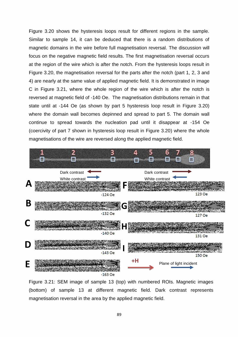
89
Figure 3.20 shows the hysteresis loops result for different regions in the sample.
Similar to sample 14, it can be deduced that there is a random distributions of
magnetic domains in the wire before full magnetisation reversal. The discussion will
focus on the negative magnetic field results. The first magnetisation reversal occurs
at the region of the wire which is after the notch. From the hysteresis loops result in
Figure 3.20, the magnetisation reversal for the parts after the notch (part 1, 2, 3 and
4) are nearly at the same value of applied magnetic field. It is demonstrated in image
C in Figure 3.21, where the whole region of the wire which is after the notch is
reversed at magnetic field of -140 Oe. The magnetisation distributions remain in that
state until at -144 Oe (as shown by part 5 hysteresis loop result in Figure 3.20)
where the domain wall becomes depinned and spread to part 5. The domain wall
continue to spread towards the nucleation pad until it disappear at -154 Oe
(coercivity of part 7 shown in hysteresis loop result in Figure 3.20) where the whole
magnetisations of the wire are reversed along the applied magnetic field.
H
G
F
E
D
C
B
A
I +H
Dark contrast
White contrast
Dark contrast
White contrast
Figure 3.21: SEM image of sample 13 (top) with numbered ROIs. Magnetic images
(bottom) of sample 13 at different magnetic field. Dark contrast represents
magnetisation reversal in the area by the applied magnetic field.
Plane of light incident
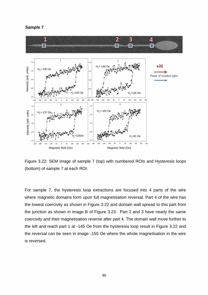
90
Sample 7
1
Magnetic field(Oe)
-250 -200 -150 -100 -50 0 50 100 150 200 250
Inte
nsity (
arb
. units)
-1.0
-0.5
0.0
0.5
1.02
Magnetic field(Oe)
-250 -200 -150 -100 -50 0 50 100 150 200 250
-1.0
-0.5
0.0
0.5
1.0
3
-250 -200 -150 -100 -50 0 50 100 150 200 250
Inte
nsity (
arb
. units)
-1.0
-0.5
0.0
0.5
1.04
-250 -200 -150 -100 -50 0 50 100 150 200 250
-1.0
-0.5
0.0
0.5
1.0
Hc=133 Oe
-Hc=-102 Oe
-Hc=-145 Oe
-Hc=-138 Oe
-Hc=-137 Oe
Hc=126 Oe
Hc=125Oe H
c=81 Oe
Figure 3.22: SEM image of sample 7 (top) with numbered ROIs and Hysteresis loops
(bottom) of sample 7 at each ROI.
For sample 7, the hysteresis loop extractions are focused into 4 parts of the wire
where magnetic domains form upon full magnetisation reversal. Part 4 of the wire has
the lowest coercivity as shown in Figure 3.22 and domain wall spread to this part from
the junction as shown in image B of Figure 3.23. Part 2 and 3 have nearly the same
coercivity and their magnetisation reverse after part 4. The domain wall move further to
the left and reach part 1 at -145 Oe from the hysteresis loop result in Figure 3.22 and
the reversal can be seen in image -155 Oe where the whole magnetisation in the wire
is reversed.
Magnetic field (Oe) Magnetic field (Oe)

91
Figure 3.23: SEM image of sample 7 (top) with numbered ROIs. Magnetic images
(bottom) of sample 7 at different magnetic field. Dark contrast represents
magnetisation reversal in the area by the applied magnetic field.
B
A
C
E
D
G
F
I
H
J
Dark contrast
White contrast
Dark contrast
White contrast

92
Sample 12
1
Magnetic field(Oe)
-250 -200 -150 -100 -50 0 50 100 150 200 250 300
Inte
nsity (
arb
. units)
-1.0
-0.5
0.0
0.5
1.02
-250 -200 -150 -100 -50 0 50 100 150 200 250 300
-1.0
-0.5
0.0
0.5
1.0
3
Magnetic field(Oe)
-250 -200 -150 -100 -50 0 50 100 150 200 250 300
Inte
nsity (
arb
. units)
-1.0
-0.5
0.0
0.5
1.0
4
Magnetic field(Oe)
-250 -200 -150 -100 -50 0 50 100 150 200 250 300
-1.0
-0.5
0.0
0.5
1.0
5
-250 -200 -150 -100 -50 0 50 100 150 200 250 300
Inte
nsity (
arb
. units)
-1.0
-0.5
0.0
0.5
1.0 6
-250 -200 -150 -100 -50 0 50 100 150 200 250 300
Inte
nsity
(arb
. units
)
-1.0
-0.5
0.0
0.5
1.0
Hc=128 Oe
-Hc=-156 Oe
-Hc=-143 Oe -H
c=-160 Oe
-Hc=-70 Oe
-Hc=-152 Oe
-Hc=-140 Oe
Hc=149 Oe
Hc=131 Oe H
c=140 Oe
Hc=116 Oe H
c=55Oe
Figure 3.24: SEM image of sample 12 (top) with numbered ROIs (regions of interest).
Hysterersis loops (bottom) of sample 12 at different ROIs.
Magnetic field (Oe) Magnetic field (Oe)
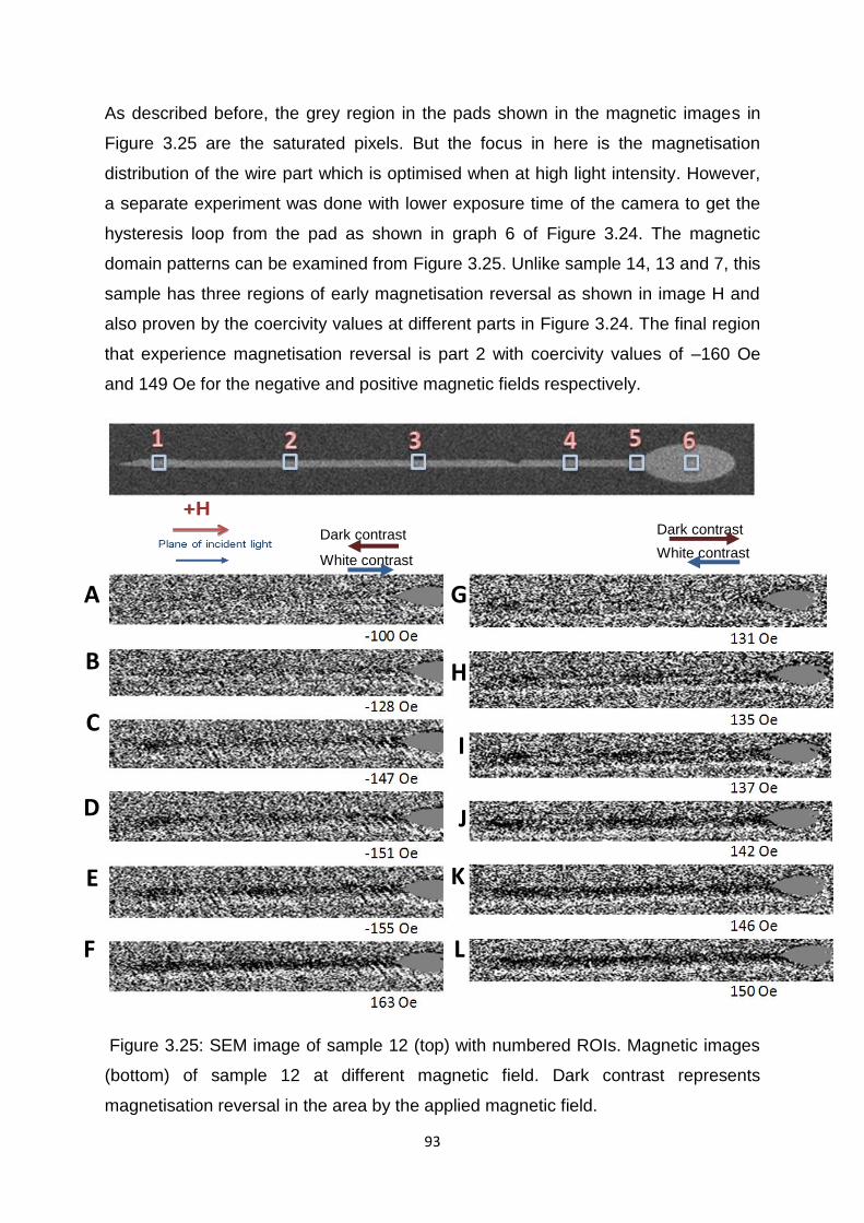
93
As described before, the grey region in the pads shown in the magnetic images in
Figure 3.25 are the saturated pixels. But the focus in here is the magnetisation
distribution of the wire part which is optimised when at high light intensity. However,
a separate experiment was done with lower exposure time of the camera to get the
hysteresis loop from the pad as shown in graph 6 of Figure 3.24. The magnetic
domain patterns can be examined from Figure 3.25. Unlike sample 14, 13 and 7, this
sample has three regions of early magnetisation reversal as shown in image H and
also proven by the coercivity values at different parts in Figure 3.24. The final region
that experience magnetisation reversal is part 2 with coercivity values of –160 Oe
and 149 Oe for the negative and positive magnetic fields respectively.
Figure 3.25: SEM image of sample 12 (top) with numbered ROIs. Magnetic images
(bottom) of sample 12 at different magnetic field. Dark contrast represents
magnetisation reversal in the area by the applied magnetic field.
A
C
B
A
D
H
E
I
F
G
L
K
J
Dark contrast
White contrast
Dark contrast
White contrast

94
Sample 6
1
-250 -200 -150 -100 -50 0 50 100 150 200 250 300
Inte
nsity (
arb
. units)
-1.0
-0.5
0.0
0.5
1.02
Magnetic field(Oe)
-250 -200 -150 -100 -50 0 50 100 150 200 250 300
-1.0
-0.5
0.0
0.5
1.0
3
Magnetic field(Oe)
-250 -200 -150 -100 -50 0 50 100 150 200 250 300
Inte
nsity (
arb
. units)
-1.0
-0.5
0.0
0.5
1.04
Magnetic field(Oe)
-250 -200 -150 -100 -50 0 50 100 150 200 250 300
-1.0
-0.5
0.0
0.5
1.0
5
-250 -200 -150 -100 -50 0 50 100 150 200 250 300
Inte
nsity (
arb
. units)
-1.0
-0.5
0.0
0.5
1.0 6
-250 -200 -150 -100 -50 0 50 100 150 200 250 300
-1.0
-0.5
0.0
0.5
1.0
Hc=124 Oe
-Hc=-126 Oe
-Hc=-134 Oe -H
c=-122 Oe
-Hc=-118 Oe
-Hc=-136 Oe
-Hc=-136 Oe
Hc=109 Oe
Hc=118 Oe H
c=113 Oe
Hc=120 Oe
Hc=98 Oe
Figure 3.26: SEM image of sample 6 (top) with numbered ROIs (regions of interest).
Hysterersis loops (bottom) of sample 6 at different ROIs.
Similar to sample 12, there are three parts that undergone early magnetisation
reversal compared to the other parts. The three parts are part 2, 4 and 6 in which their
reversals can be observed in image C at magnetic field of -128 Oe and also image H
at magnetic field 119 Oe both in Figure 3.27. Referring to the hysteresis loops result in
Figure 3.26, the two last magnetisation reversals occur together at part 5 and 1. This
concludes that the domain wall produced from the junction at the pad and the wire did
not progress to the notch, not until when the magnetisation in part 5 reversed, then
after that the domain walls disappear.
Magnetic field (Oe) Magnetic field (Oe)
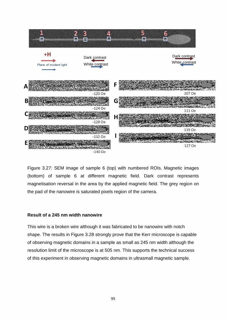
95
Figure 3.27: SEM image of sample 6 (top) with numbered ROIs. Magnetic images
(bottom) of sample 6 at different magnetic field. Dark contrast represents
magnetisation reversal in the area by the applied magnetic field. The grey region on
the pad of the nanowire is saturated pixels region of the camera.
Result of a 245 nm width nanowire
This wire is a broken wire although it was fabricated to be nanowire with notch
shape. The results in Figure 3.28 strongly prove that the Kerr microscope is capable
of observing magnetic domains in a sample as small as 245 nm width although the
resolution limit of the microscope is at 505 nm. This supports the technical success
of this experiment in observing magnetic domains in ultrasmall magnetic sample.
C
B
E
D
G
F
I
H
A
Dark contrast
White contrast
Dark contrast
White contrast

96
164 Oe
201 Oe
Figure 3.28: SEM image of the 245 nm width nanowire (top) and magnetic
images (bottom) at different magnetic fields. The magnetic images prove that the
Kerr microscope setup is capable of observing magnetic image of sample as
small as 245 nm widths.
3.6.4 Discussion
In general, the examined results of the group two wires agree with the
magnetostatic energy and shape anisotropy effects on the samples which cause
the lower coercivity of the nucleation pad than the nanowire. Moreover, the
magnetisation direction is along the easy axis for the wire part and for the
nucleation pad the magnetisation directions are forming vortex along the edges.
A new phenomenon is observed in the group two wires where there are multiple
magnetic domains formation upon magnetisation reversal. This could open a new
path of research for the possible application of this new behaviour of notched
wire with nucleation pad. The magnetic domains pattern is repeatable and forms
at both positive and negative applied magnetic fields. Therefore, each domain

97
can be encoded as storage information and has the possibility to be used as
magnetic storage devices. As seen from the hysteresis loop results, the
asymmetric notch caused different coercivity values at positive and negative
applied magnetic field. This is caused mainly by the introduction of notch at the
wire.
It is deduced that the reason for the low coercivities difference at areas before
and after the notch is because of the high coercivity of the nucleation pad. Similar
experiment done using a more circular nucleation pad resulted in a large
coercivities difference and is caused by the pinning of domain wall at the notch
[34]. This is also proven by the simulation results where the domain wall forms at
higher magnetic field and the pinning of domain wall is very weak as shown in
Figure 3.19.
Coercivity difference between after notch and before
notch compared to the percentage notch width
Percentage of notch depth to the wire width(%)
25 30 35 40 45 50 55 60
Ma
gne
tic fie
ld(O
e)
-10
-5
0
5
10
15
Coercivity at negative magnetic field
Figure 3.29: Graph showing the relation between the coercivities difference
before and after notch with the percentage notch depth.
Instead of strong pinning effect of domain wall at the notch, the wires form multi
domains upon reversal giving a non-linear relationship of the coercivities
Percentage of notch depth to the wire width (%)
Graph of coercivity difference between the areas after notch
and before notch versus the percentage notch depth to the wire
width
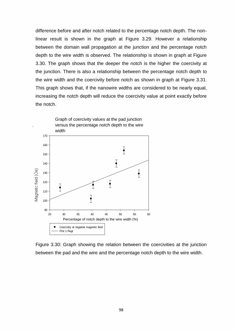
98
difference before and after notch related to the percentage notch depth. The non-
linear result is shown in the graph at Figure 3.29. However a relationship
between the domain wall propagation at the junction and the percentage notch
depth to the wire width is observed. The relationship is shown in graph at Figure
3.30. The graph shows that the deeper the notch is the higher the coercivity at
the junction. There is also a relationship between the percentage notch depth to
the wire width and the coercivity before notch as shown in graph at Figure 3.31.
This graph shows that, if the nanowire widths are considered to be nearly equal,
increasing the notch depth will reduce the coercivity value at point exactly before
the notch.
Coercivity values at junction between wire and pad
Percentage of notch depth to the wire width(%)
25 30 35 40 45 50 55 60
Ma
gne
tic fie
ld(O
e)
90
100
110
120
130
140
150
160
170
Coercivity at negative magnetic field
Plot 1 Regr
Figure 3.30: Graph showing the relation between the coercivities at the junction
between the pad and the wire and the percentage notch depth to the wire width.
Percentage of notch depth to the wire width (%)
Graph of coercivity values at the pad junction
versus the percentage notch depth to the wire
width

99
Coercivity values before notch
Percentage of notch depth to the wire width(%)
25 30 35 40 45 50 55 60
Ma
gne
tic fie
ld(O
e)
110
120
130
140
150
160
170
180
Coercivity at negative magnetic field
Coercivity at positive magnetic field
Figure 3.31: Graph showing the relationship between the coercivity before notch
and percentage notch depth to the wire width.
4. Summary and conclusions
It has been demonstrated that the Kerr microscope is capable of observing
magnetic domains in a sample as small as 245 nm width although the resolution
limit of the microscope is at 505 nm. The Kerr microscopy setup makes it
possible for the observation of magnetic field driven domain wall propagation in
magnetic nanowires. This could be the first wide-field microscopy setup which
demonstrated the ability to produce magnetic domains image from magnetic
nanostructures. Kerr microscopy remains as the best method for visualization of
moving domains in the laboratory due to its flexibility and versatility. Following the
outstanding capability of imaging domain motions in nanowire as proven in this
research project, it is therefore the most suitable method for magnetic nanowire
observation. Furthermore, the ‘homemade’ Kerr microscopy will exceed the limits
of commercial wide-field microscopy such as the introduction of cryostats or
heating stage at the sample holder. The combination of hysteresis loops and
Percentage of notch depth to the wire width (%)
Graph of coercivity values before notch versus
percentage notch depth to wire width
100
magnetic domains observations for studying a magnetic sample helps to provide
a three-dimensional understanding of the magnetic characteristic of the sample.
This is important in investigating nanosamples where the theoretical arguments
with the experimental results are always limited by the experimental part. The
images captured during the experiment are all saved for future use, thus the data
can be analysed so many times for new findings. Therefore, the experiment does
not require a repetition if a hysteresis loop result is needed in different part of the
sample which is the case for the MOKE magnetometry method. Digital image
enhancement helps to increase domains contrast for small objects with very
weak Kerr effect. Image averaging from repeated cycles have shown to cause
significant contrast enhancement to the magnetic domains image. The Kerr
microscopy setup is proven to be capable of investigating Kerr effect at different
MOKE geometry.
From the nano objects results, the final image shows an extremely strong
domains contrast which have never been achieved before by using wide field
microscopy. The observed magnetisation distributions in the nano samples are
caused by the magnetostatic energy and the shape anisotropy effect. Domains
walls propagation plays an important role in causing magnetisation reversal at
lower magnetic field in nanowire. The observed magnetisation alignment along
the easy axis of the nanowire confirms with the magnetostatic energy and shape
anisotropy theories. Both cross and zigzag nanowires formed multiple domains
upon magnetisation reversal and their magnetisation behaviour can be analysed
in further detail by observing their hysteresis loops and also their magnetic
domains image results.
For the nanowire with notch, the elliptical pad is proven to have lower coercivity
than the wire due to shape anisotropy. The observation of weak domain wall
pinning by the notch is mainly caused by the large coercivity of the elliptical pad
because a lower coercivity nucleation pad is essential so that the domain wall
formed will start to progress at lower field. A relationship between the percentage
notch depth with the coercivity at the junction was observed in which when
increasing the percentage notch depth, the coercivity at the junction increase.

101
Overall, the microscope setup alongside the developed programmes has proved
to be an outstanding method for in-depth investigation of magnetic nano objects.
4.1 Further work
With the unlimited new types of nano structures which can be fabricated, the set
up can be used further for magnetic domains observations of these nano objects.
With the newly achieved high domain contrasts image, a variety of
nanostructures can be investigated. A temperature dependent experiment on
nanowires with notch can be done in the future by using the setup. A domain wall
pinning experiments for different nucleation pad and different notch shapes can
be continued. A temperature dependent domain wall motion visualisation can be
done in the future as this setup is proven to produce very strong magnetic
domains for small magnetic structures. Experiments that focus on different
coercivities at positive and negative fields can give a new understanding of the
magnetic properties of nanowire. With the flexibility and versatility of the Kerr
microscope, unlimited experiments on magnetic nano objects can be performed.

102
5. Appendices
5.1 Appendix 1: Programme to extract the hysteresis loop for the magneto-
optical magnetometry
5.2 Appendix 2: Programme for taking a sets of pictures with known
magnetic field for each picture

103
5.3 Appendix 3: Programme to analyse the sets of images and to do digital
contrast enhancement
104
6. Bibliography
[1] B.D Cullity and C.D Graham, Introduction to Magnetic Materials, second
edition, Wiley(2009), pp1-2, 115, 102.
[2] Available at <http://www.recording-history.org/HTML/wire2.php> [Acessed: 31
January 2013].
[3] Available at <http://www.emc.com/collateral/analyst-reports/diverse-
exploding-digital-universe.pdf> [Acessed: 31 January 2013].
[4] Available at <https://www.ibm.com/developerworks/mydeveloperworks/
blogs/storagevirtualization/entry/a_brief_history_of_access_density1?lang=en>
[Acessed: 31 January 2013].
[5] M. Tsoi, R. E. Fontana, S. S. P. Parkin, “Magnetic domain wall motion
triggered by an electric current”, ppl. Phys. Lett. 83, 2617 (2003).
[6] Parkin S S P, Hayashi M and Thomas L, “Magnetic Domain-Wall Racetrack
Memor”, Science 320 190 (2008).
[7] M. T. Bryan, T. Schrefl, D. A. Allwood, “Symmetric and asymmetric domain
wall diodes in magnetic nanowires”, Appl. Phys. Lett. 91, 142502 (2007).
[8] D. A. Allwood, G. Xiong, C. C. Faulkner, D. Atkinson, D. Petit, and R.
P.Cowburn, ”Magnetic Domain-Wall Logic”, Science 309, 1688 (2005).
[9] Weiss, P., “La variation du ferromagnetisme avec la temperature” (The
variation of ferromagnetism with temperature) Comptes Rendus 143 (1906), pp
1136-1139.
[10] Weiss, P., “L’Hypothese du champ moleculaire et de la propriete
ferromagnetique”, (The hypothesis of the molecular field and the property of
ferromagnetism) Journal de Physique et le Radium 6 (1907), pp 661-690.
[11] David Jiles, Introduction to Magnetism and Magnetic materials, Second
Edition, Published by: Chapman & Hall, (1998), p138.

105
[12] Amikam Aharoni, Introduction to The Theory of Ferromagnetism, second
edition, Oxford University Press (2007), P 5, 35.
[13] Available at <url:http://physics.unl.edu/~tsymbal/teaching/SSP-
927/Section%2016_Magnetic_ Properties_2.pdf> [Accesssed: 31 January 2013].
[14] Available at <url:http://physics.unl.edu/~tsymbal/teaching/SSP-
927/Section%2016_Magnetic _Properties_2.pdfPhysics 927 E.Y.Tsymbal 1
Section 16: Magnetic properties of materials (continued).> [Acessed: 31 January
2013].
[15] Heisenberg, W., “Zur theorie des ferromagnetismus” (On the theory of
ferromagnetism) Zeitschrift fur Physik A 49 (1928), pp 619-636.
[16] Available at <url: http://www.ndt-ed.org/EducationResources/ Community
College/MagParticle/Physics/HysteresisLoop.htm> [Acessed: 31 January 2013].
[17] Sixtus, K. J., and Tonks, L., “Propagation of large Barkhausen
discontinuities”, Physical Review 37 (1931), pp930-958.
[18] Bitter, F., “Experiments on the nature of ferromagnetism”, Physical Review
41 (1932), pp 507-515.
[19] Landau, L.D., and Lifshitz, E., “On the theory of the dispersion of magnetic
permeability in ferromagnetic bodies”, Physikalische Zeitschrift der Sowjetunion 8
(1935), pp 153-169.
[20] Available at:<http://www.birmingham.ac.uk/research/activity/metallurgy-
materials/magnets/background/magnetic-materials-domains.aspx> [Acessessed:
31 January 2013].
[21] Bruce M. Moskowitz. (1991), Hitchhiker's Guide to Magnetism, Available at
<url: http://www.irm.umn.edu/hg2m/hg2m_c/hg2m_c.html.> [Accessed: 27th, Jan,
2013].
[22] Kronmuller H., and Fahnle M., Micromagnetisation and the microstructure of
ferromagnetic solids Cambridge University Press, Cambridge (2003).

106
[23] Robert C. O’Handley, Modern Magnetic Materials Principles and
Applications, Wiley-Interscience Publication (2003), p 184, 289.
[24] Bozorth, R. M., “Directional ferromagnetic properties of metals”, Journal of
Applied Physics 8 (1937), pp 575-588.
[25] Available at <url:http://physics.unl.edu/~tsymbal/teaching/SSP-927/Section%
2016_Magnetic _Properties_2.pdfPhysics 927 E.Y.Tsymbal 1 Section 16:
Magnetic properties of materials (continued). > [Acessed: 18 January 2013].
[26] Neel, L., “Energie des parois de Bloch dans les couches minces” (Bloch wall
energy in thin films) Comptes Rendus de l’Academie des Sciences 241 (1955),
pp 533-536.
[27] Available at <url:http://www.solutioninn.com/physics/solid-state/general-
problem/neel-wall-the-direction-of-magnetization-change-in-domain> [Acessed:
31 January 2013].
[28] M. Herrmann, S. McVitie, and J. N. Chapman, “Investigation of the influence
of edge structure on the micromagnetic behavior of small magnetic elements”, J.
Appl. Phys. 87, 2994 (2000).
[29] X. Liu, J. N. Chapman, S. McVitie, and C. D. W. Wilkinson,” Reversal
mechanisms and metastable states in magnetic nanoelements”, J. Appl. Phys.
96, 5173 (2004).
[30] Available at <url:http://www.magnetics.group.shef.ac.uk/? Research:Patterne
d_magnetic_structures> [Acessed: 31 January 2013].
[31] Yoshinobu Nakatani, Andre´ Thiaville, Jacques Miltat, “Head-to-head domain
walls in soft nano-strips: a refined phase diagram”, Journal of Magnetism and
Magnetic Materials 290–291 750–753 (2005).
[32] Diegel, M., Mattheis, R., and Halder E., “360° domain wall investigation for
sensor applications” IEEE Transactions of Magnetics 40 (2004), pp 2655-2657.
107
[33] Weiwei Zhu, Jialin Liao, Zongzhi Zhang, B. Ma, Q.Y Jin, ” Depinning of
vortex domain walls from an asymmetric notch in a permalloy”, Nanowire,Appl.
Phys. Lett. 101, 082402 (2012).
[34] P. R. Cantwell, U. J. Gibson, D. A. Allwood, and H. A. M. Macleod, “Optical
coatings for improved contrast in longitudinal magneto-optic Kerr effect
measurements”, J. Appl. Phys. 100, 093910 (2006).
[35] J. N. Chapman, “The investigation of magnetic domain structures in thin foils
by electron microscopy”, J. Phys. D: Appl. Phys. 17, 623 (1984).
[36] H. Lichte and M. Lehmann, “Electron holography—basics and applications”,
Rep. Prog. Phys. 71, 016102 (2008).
[37] S. Hankemeier, A. Kobs, R. Fro¨mter, and H. P. Oepen, “Controlling the
properties of vortex domain walls via magnetic seeding fields”, Phys. Rev. B 82,
064414 (2010).
[38] S. Krause, G. Herzog, T. Stapelfeldt, L. Berbil-Bautista, M. Bode, E. Y.
Vedmedenko, and R. Wiesendanger, “Magnetization Reversal of Nanoscale
Islands: How Size and Shape Affect the Arrhenius Prefactor”, Phys. Rev. Lett.
103, 127202 (2009).
[39] J. P. Davis, D. Vick, D. C. Fortin, J. A. J. Burgess, W. K. Hiebert, and M.
R. Freeman, “Nanotorsional resonator torque magnetometry”, Appl. Phys. Lett.
96, 072513 (2010).
[40] W. Wernsdorfer, “From micro- to nano-SQUIDs: applications to nano-
magnetism”, Supercond. Sci. Technol. 22, 064013 (2009).
[41] P. Weinberger, “John Kerr and his effects found in 1877 and 1878”,
Philosophical Magazine Letters, 88:12, 897-907 (2008).
108
[42] Faraday, M., "On the magnetisation of light and the illumination of magnetic
lines of force”, Philosophical Transactions of the Royal Society (London) 136, 1-
20 (1846).
[43] A. Hubert, R. Schäfer, Magnetic Domains,The analysis of magnetic micro-
structures, (Berlin) Springer-Verlag Berlin and Heidelberg GmbH & Co. KG
(1999).
[44] R. Schafer, “Investigation of domains and dynamics of domain Walls by the
magneto-optical Kerr-effect”, Handbook of Magnetism and Advanced Magnetic
Materials, John Willey & Sons (2007).
[45] G. S. Krinchik and V. A. Artem’ev, “Magneto-optical Properties Of Ni, Co,
And Fe In The Ultraviolet Visible, And Infrared Parts Of The Spectrum”, Soviet
Physics Jept Volume 26, No 6 1968 [Zh. Eksp. Teor. Fiz. 53, 1901-1912
(December, 1967)].
[46] J. Zak, E. R. Moog, C. Liu, and S. D. Bader, “Fundamental magneto-optics”,
J. Appl. Phys. 68, 4203 (1990).
[47] J. M. Florczak and E. Dan Dahlberg, “Detecting two magnetization compo-
nents by the magneto-optical Kerr effect”, J. Appl. Phys. 67, 7520 (1990).
[48] C. You and S. Shin, “Effects of polarizer and analyzer imperfections in a
magneto-optical Kerr spectrometer”, J. Opt. Soc. Am. B 17, 910-913 (2000).
[49] Available at <url :http://www.olympusmicro.com/primer/techniques/fluorescen
ce/anatomy/fluoromicroanatomy.html> [accessed at: 31 January 2013].
[50] Ambar, H., Y. Aoki, N. Takai, and T. Asakura, “Mechanism of speckle
reduction in laser-microscope images using a rotating optical fiber”, Applied
Physics B: Lasers and Optics 38, no. 1, 71-78 (1985).
[51] Available at <url :http://www.mitutoyo.com/pdf/E4191-378_010611.pdf >
[Accessed: 31 January 2013].

109
[52] Available at <url:http://sales.hamamatsu.com/assets/pdf/hpspdf/C4742-95-
12ER.pdf > [Accessed: 31 January 2013].
[53] Available at <url:Code package http://math.nist.gov/> [Accessed on 31
January 2013].
[54] Gilbert, T. L., “A phenomenological theory of damping in ferromagnetic
materials”, IEEE Trans. Magn. 40, 3443-3449 (2004).
[55] Serban Lepadatu (2006), ”Domain wall scattering and current induced
magnetic switching in patterned ferromagnetic nanowires”, PhD thesis, The
University of York.
[56] D. S. Eastwood, J. A. King, L. K. Bogart, H. Cramman, and D. Atkinson ,
“Chirality-dependent domain wall pinning in a multinotched planar nanowire and
chirality preservation using transverse magnetic fields”, J. Appl. Phys. 109,
013903 (2011).
[57] Dorothée Petit, Ana-Vanessa Jausovec, Dan Read, and Russell P. Cowburn,
“Domain wall pinning and potential landscapes created by constrictions and
protrusions in ferromagnetic nanowires”. J. Appl. Phys. 103, 114307 (2008).
[58] Y. B. Xu, C. A. F. Vaz, A. Hirohata, H. T. Leung, C. C. Yao, and J. A. C,
“Bland Magnetoresistance of a domain wall at a submicron junction”, Physical
Review B Vol 61, NUMBER 22 (2000).
[59] A. Hirohata, C. C. Yao, H. T. Leung, Y. B. Xu, C. M. Guertler, and J. A. C.
Bland, “Magnetic Domain Studies of Permalloy Wire-Based Structures with
Junctions”, IEEE TRANS. M., VOL. 36, NO. 5 (2000).
[60] Weiwei Zhu, Jialin Liao, Zongzhi Zhang, B. Ma, Q.Y Jin, “Depinning of
vortex domain walls from an asymmetric notch in a permalloy nanowire”, Appl.
Phys. Lett. 101, 082402 (2012).

110
[61] D. McGrouther, S. McVitie, J. N. Chapman and A. Gentils, “Controlled
domain wall injection into ferromagnetic nanowires from an optimized pad
geometry”, Appl. Phys. Lett. 91, 022506 (2007).
[62] Mi-Young Im, Lars Bocklage, Peter Fischer and Guido Meier, “ Direct
Observation of Stochastic Domain-Wall Depinning in Magnetic Nanowires”, PRL
102, 147204 (2009).