magnetic sensor - memsic.com · memsic mmc3416xpj rev c page 3 of 13 10/30/2013 i2c interface i/o...
TRANSCRIPT

MEMSIC MMC3416xPJ Rev C Page 1 of 13 10/30/2013
h
±16 Gauss, Ultra Small, Low Noise 3-axis Magnetic Sensor
MMC3416xPJ
FEATURES Fully integrated 3-axis magnetic sensor and
electronic circuits requiring fewer external
components
Superior Dynamic Range and Accuracy:
±16 G FSR with 16/14 bits operation
0.5 mG/2 mG per LSB resolution in 16/14
bits operation mode
1.5 mG total RMS noise
Enables heading accuracy of 1º
Max output data rate of 800 Hz (12 bits mode)
Ultra Small Low profile package
1.6x1.6x0.6 mm
SET/RESET function
Allows for elimination of temperature
variation induced offset error (Null field
output)
Clears the sensors of residual
magnetization resulting from strong
external fields
On-chip sensitivity compensation
Low power consumption (140 µA @ 7 Hz )
1 µA (max) power down function
I2C Slave, FAST (≤400 KHz) mode
1.62 V~3.6 V wide power supply operation
supported, 1.8 V I/O compatibility.
RoHS compliant
APPLICATIONS Electronic Compass & GPS Navigation
Position Sensing
DESCRIPTION
The MMC3416xPJ is a complete 3-axis magnetic sensor with on-chip signal processing and integrated I2C bus. The device can be connected directly to a
microprocessor, eliminating the need for A/D converters or timing resources. It can measure
magnetic fields within the full scale range of 16 Gauss (G), with 0.5 mG/2 mG per LSB resolution for 16/14 bits operation mode and 1.5 mG total RMS
noise level, enabling heading accuracy of 1º in electronic compass applications. Contact MEMSIC for access to advanced calibration and tilt-compensation algorithms.
An integrated SET/RESET function provides for the elimination of error due to Null Field output change with temperature. In addition it clears the sensors of any residual magnetic polarization resulting from exposure to strong external magnets. The SET/RESET function can be performed for each measurement or periodically as the specific application requires.
The MMC3416xPJ is packaged in an ultra small low profile BGA package (1.6 x 1.6 x 0.6 mm,) and with an
operating temperature range from -40 C to +85 C.
The MMC3416xPJ provides an I2C digital output with
400 KHz, fast mode operation.
Information furnished by MEMSIC is believed to be accurate and reliable. However, no responsibility is assumed by MEMSIC for its use, or for any infringements of patents or other rights of third parties which may result from its use. No license is granted by implication or otherwise under any patent or patent rights of MEMSIC.
MEMSIC, Inc.
One Technology Drive, Suite 325, Andover, MA01810, USA
Tel: +1 978 738 0900 Fax: +1 978 738 0196
www.memsic.com
FUNCTIONAL BLOCK DIAGRAM

MEMSIC MMC3416xPJ Rev C Page 2 of 13 10/30/2013
SPECIFICATIONS (Measurements @ 25 C, unless otherwise noted; VDA = VDD= 1.8 V unless otherwise specified)
Parameter Conditions Min Typ Max Units
Field Range (Each Axis)
Total applied field 16 G
Supply Voltage VDA 1.621 1.8 3.6 V
VDD (I2C interface) 1.62
1 1.8 3.6 V
Supply Voltage Rise Time 5.0 mS
Supply Current2 (7measurements/second)
BW[1:0]=00, 16 bits mode 140 µA
BW[1:0]=01, 16 bits mode 70 µA
BW[1:0]=10, 14 bits mode 35 µA
BW[1:0]=11, 12 bits mode 18 µA
Power Down Current 1.0 µA
Operating Temperature -40 85 C
Storage Temperature -55 125 C
Linearity Error (Best fit straight line)
FS=±16 G Happlied=±10 G
0.25 %FS
Hysteresis 3 sweeps across ±16 G 0.1 %FS
Repeatability Error 3 sweeps across ±16 G 0.1 %FS
Alignment Error 1.0 3.0 degrees
Transverse Sensitivity 2.0 5.0 %
Total RMS Noise
BW[1:0]=00, 16 bits mode 1.5 mG
BW[1:0]=01, 16 bits mode 2.0 mG
BW[1:0]=10, 14 bits mode 4.0 mG
BW[1:0]=11, 12 bits mode 6.0 mG
Output resolution 16/14/12 bits
Max Output data rate
BW[1:0]=00, 16 bits mode 125 Hz
BW[1:0]=01, 16 bits mode 250 Hz
BW[1:0]=10, 14 bits mode 450 Hz
BW[1:0]=11, 12 bits mode 800 Hz
Heading accuracy3 1.0 degrees
Sensitivity
16 G -10 +10 %
16 bits mode 2048 counts/G
14 bits mode 512 counts/G
12 bits mode 128 counts/G
Sensitivity Change Over Temperature
-40~85C
Delta from 25C
16 G
3 %
Null Field Output
±0.1 G
16 bits mode 32768 counts
14 bits mode 8192 counts
12 bits mode 2048 counts
Null Field Output Change Over Temperature using SET/RESET
-40~85 C
Delta from 25 C 5 mG
Disturbing Field4 25 G
Maximum Exposed Field 10000 G
SET/RESET Repeatability5 3 mG
11.62 V is the minimum operation voltage, or VDA / VDD should not be lower than 1.62 V. 2 Supply current is proportional to how many measurements performed per second, for example, at one measurement per second, the power consumption will be 140 uA/7=20 µA. 3 MEMSIC product enables users to utilize heading accuracy to be 1.0 degree typical when using MEMSIC’s proprietary software or algorithm 4 This is the magnitude of external field that can be tolerated without changing the sensor characteristics. If the disturbing field is exceeded, a SET/RESET operation is required to restore proper sensor operation. 5 Perform SET/RESET alternately. SET repeatability is defined as the difference in measurement between multiple SET events. RESET repeatability is defined similarly.

MEMSIC MMC3416xPJ Rev C Page 3 of 13 10/30/2013
I2C INTERFACE I/O CHARACTERISTICS (VDD=1.8 V)
Parameter Symbol Test Condition Min. Typ. Max. Unit
Logic Input Low Level VIL -0.5 0.3* VDD V
Logic Input High Level VIH 0.7*VDD VDD V
Hysteresis of Schmitt input Vhys 0.2 V
Logic Output Low Level VOL 0.4 V
Input Leakage Current Ii 0.1VDD<Vin<0.9VDD -10 10 µA
SCL Clock Frequency fSCL 0 400 kHz
START Hold Time tHD;STA 0.6 µS
START Setup Time tSU;STA 0.6 µS
LOW period of SCL tLOW 1.3 µS
HIGH period of SCL tHIGH 0.6 µS
Data Hold Time tHD;DAT 0 0.9 µS
Data Setup Time tSU;DAT 0.1 µS
Rise Time tr From VIL to VIH 0.3 µS
Fall Time tf From VIH to VIL 0.3 µS
Bus Free Time Between STOP and START
tBUF 1.3 µS
STOP Setup Time tSU;STO 0.6 µS
Timing Definition
SDA
SCL
tf tr tLOW
tHD;STA tHD;DAT tHIGH
tSU;DAT
tSU;STA
tHD;STA
Sr S
tSU;STO
tSP
S P
tf tr tBUF

MEMSIC MMC3416xPJ Rev C Page 4 of 13 10/30/2013
ABSOLUTE MAXIMUM RATINGS* Supply Voltage (VDD) ………………...-0.5 to +3.6 V
Storage Temperature ……….……-55 C to +125 C Maximum Exposed Field ………………..10000 G *Stresses above those listed under Absolute Maximum Ratings may cause permanent damage to the device. This is a stress rating only; the functional operation of the device at these or any other conditions above those indicated in the operational sections of this specification is not implied. Exposure to absolute maximum rating conditions for extended periods may affect the device’s reliability.
Pin Description: BGA Package
All parts are shipped in tape and reel packaging with 9000pcs per 13” reel or 3000pcs per 7” reel.
Caution: ESD (electrostatic discharge) sensitive device.
Ordering Guide: MMC3416xPJ
Marking illustration:
Note: Coordinates shown above indicate polarity after a SET operation.
Number Part number
0 MMC34160PJ
1 MMC34161PJ
2 MMC34162PJ
3 MMC34163PJ
4 MMC34164PJ
5 MMC34165PJ
6 MMC34166PJ
7 MMC34167PJ
“Number” represents the character of the 1
st line in
the marking, the black dot indicates pin one (1). The 2
nd line represents Lot Number.
THEORY OF OPERATION
The Anisotropic Magneto-Resistive (AMR) sensors are special resistors made of permalloy thin film deposited on a silicon wafer. During manufacturing, a strong magnetic field is applied to the film to orient its magnetic domains in the same direction, establishing a magnetization vector. Subsequently, an external magnetic field applied perpendicularly to the sides of the film causes the magnetization to rotate and change angle. This effect causes the film’s resistance to vary with the intensity of the applied magnetic field. The MEMSIC AMR sensor is incorporated into a Wheatstone bridge configuration to maximize Signal to Noise ratio. A change in magnetic field produces a proportional change in differential voltage across the Wheatstone bridge
However, the influence of a strong magnetic field (more than 25 G) in any direction could upset, or flip, the polarity of the film, thus changing the sensor characteristics. A strong restoring magnetic field must be applied momentarily to restore, or set, the sensor characteristics. The MEMSIC magnetic sensor has an on-chip magnetically coupled strap: a SET/RESET strap pulsed with a high current, to provide the restoring magnetic field.
Pin Name Description I/O
1 TEST Factory Use Only, Leave Open/Not connected
NC
2 NC Not Connected NC
3 SCL Serial Clock Line for I
2C
bus I
4 SDA Serial Data Line for I2C bus I/O
5 Vpp Factory Use Only, Leave Open
NC
6 VDD Power Supply for I2C bus P
7 NC Not Connected NC
8 CAP Connect to External Capacitor
I
9 NC Not Connected NC
10 NC Not Connected NC
11 VSA Connect to Ground P
12 VDA Power Supply P
Address code: 0~7
Code 7 bit I2C
Address
0 0110000b
1 0110001b
2 0110010b
3 0110011b
4 0110100b
5 0110101b
6 0110110b
7 0110111b
Package type:
Code Type
J BGA12
RoHS compliant
Performance Grade:
Code Performance Grade
P Temp compensated

MEMSIC MMC3416xPJ Rev C Page 5 of 13 10/30/2013
PIN DESCRIPTIONS
VDA – This is the supply input for the circuits and the magnetic sensor. The DC voltage should be between 1.62 and 3.6 volts. A 1uF by-pass capacitor is strongly recommended.
VSA – This is the ground pin for the magnetic sensor.
SDA – This pin is the I2C serial data line, and operates
in FAST (400 KHz) mode.
SCL– This pin is the I2C serial clock line, and operates
in FAST (400 KHz) mode.
VDD – This is the power supply input for the I2C bus,
and is 1.8 V compatible (1.62 V to 3.6 V). VDD is independent of VDA.
TEST – Factory use only, Leave Open/Not connected
CAP –Connect a 4.7 µF low ESR (typically smaller than 0.2 ohm) ceramic capacitor.
Vpp – Factory use only, Leave Open
EXTERNAL CIRCUITRY CONNECTION
(Top View)
HARDWARE DESIGN CONSIDERATION
Provide adequate separation distance to devices that contain permanent magnets or generate magnetic fields (IE speakers, coils, inductors...) The combined magnetic field to be measured and interference magnetic field should be less than the full scale range of the MMC3416xPJ (±16 G).
Provide adequate separation distance to current carrying traces. Do not route current carrying traces under the sensor or on the other side of the PCB opposite the device.
Do not cover the sensor with magnetized material or material that may become magnetized, (IE, shield box, LCD, battery, iron bearing material…).
Do not place the device opposite magnetized material or material that may become magnetized located on the other side of the PCB.
Please refer to MEMSIC application note: AN-200-20-0001 (MEMSIC Magnetic Sensor Hardware Design Layout Guideline for Electronic Device).
POWER CONSUMPTION
The power consumed by the device is proportional to the number of measurements taken per second. For example, when BW<1:0>=00, that is, 16-bit mode with 7.92 mS per measurement, MMC3416xPJ consumes 140 µA (typical) at 1.8 V with 7 measurements per second. If only 2 measurements are performed per second, the current will be 140*2/7=40 µA.
I2C INTERFACE DESCRIPTION
A slave mode I2C circuit has been implemented into
the MEMSIC magnetic sensor as a standard interface for customer applications. The A/D converter and MCU functionality have been added to the MEMSIC sensor, thereby increasing ease-of-use, and lowering power consumption, footprint and total solution cost.
The I2C (or Inter IC bus) is an industry standard bi-
directional two-wire interface bus. A master I2C device
can operate READ/WRITE controls to an unlimited number of devices by device addressing. The MEMSIC magnetic sensor operates only in a slave mode, i.e. only responding to calls by a master device.
I2C BUS CHARACTERISTICS
I2C Bus
The two wires in the I2C bus are called SDA (serial
data line) and SCL (serial clock line). In order for a data transfer to start, the bus has to be free, which is defined by both wires in a HIGH output state. Due to the open-drain/pull-up resistor structure and wired Boolean “AND” operation, any device on the bus can pull lines low and overwrite a HIGH signal. The data
Rp Rp
SDA (Serial Data Line)
SCL (Serial Clock Line)
DEVICE 1
DEVICE 2
VDD

MEMSIC MMC3416xPJ Rev C Page 6 of 13 10/30/2013
on the SDA line has to be stable during the HIGH period of the SCL line. In other words, valid data can only change when the SCL line is LOW.
Note: Rp selection guide: 4.7 Kohm for a short I2C
bus length (less than 10 cm), and 10Kohm for a bus length less than 5 cm.
REGISTER MAP
Register Name Address Description
Xout Low 00H Xout LSB
Xout High 01H Xout MSB
Yout Low 02H Yout LSB
Yout High 03H Yout MSB
Zout Low 04H Zout LSB
Zout High 05H Zout MSB
Status 06H Device status
Internal control 0 07H Control register 0
Internal control 1 08H Control register 1
R0 1BH Factor used register
R1 1CH Factory used register
R2 1DH Factory used register
R3 1EH Factory used register
R4 1FH Factory used register
Product ID 1 20H Product ID
Register Details
Xout High, Xout Low
Xout Low 7 6 5 4 3 2 1 0
Addr: 00H Xout[7:0]
Mode R
Xout High 7 6 5 4 3 2 1 0
Addr: 01H Xout[15:8]
Mode R
X-axis output, unsigned format, the 2 LSB of Xout Low will be fixed as “0” when in 12 bit mode, the 2 LSB of Xout Low will be fixed as “0” when in 14 bit mode.
Yout High, Yout Low
Yout Low 7 6 5 4 3 2 1 0
Addr: 02H Yout[7:0]
Mode R
Yout High 7 6 5 4 3 2 1 0
Addr: 03H Yout[15:8]
Mode R
Y-axis output, unsigned format, the 2 LSB of Yout Low will be fixed as “0” when in 12 bit mode, the 2 LSB of Yout Low will be fixed as “0” when in 14 bit mode.
Zout High, Zout Low
Zout Low 7 6 5 4 3 2 1 0
Addr: 04H Zout[7:0]
Mode R
Zout High 7 6 5 4 3 2 1 0
Addr: 05H Zout[15:7]
Mode R
Z-axis output, unsigned format, the 2 LSB of Zout Low will be fixed as “0” when in 12 bit mode, the 2 LSB of Zout Low will be fixed as “0” when in 14 bit mode.

MEMSIC MMC3416xPJ Rev C Page 7 of 13 10/30/2013
Status
Device Status 7 6 5 4 3 2 1 0
Addr: 06H Reserved ST_XYZ
_OK Rd_Done Pump
On Meas Done
Reset Value 0 0 0 0 0 0 0 0
Mode R
Bit Name Description
Meas Done Indicates measurement event is completed. This bit should be checked before reading the output
Pump On Indicates the charge pump status, after Refill Cap command, the charge pump will start running, and this bit will stays high, it will be reset low after the cap reaches its target voltage and the charge pump is shut off.
Rd_Done Indicates the chip was able to successfully read its memory.
ST_XYZ_OK Indicate selftest OK once this bit is “1”.
Internal Control 0
Control
Register 0
7 6 5 4 3 2 1 0
Addr: 07H Refill Cap
RESET SET No Boost
CM Freq1
CM Freq0
Cont Mode
On
TM
Reset Value 0 0 0 0 0 0 0 0
Mode W W W W W W W W
Bit Name Description
TM Take measurement, set ‘1’ will initiate measurement.
Cont Mode On When set to a 1 this enables the Continuous Measurement Mode. The chip will periodically take measurements of the magnetic field; the frequency of these measurements is determined by bits CM Freq<1:0>.
CM Freq0 & CM Freq1
These bits determine how often the chip will take measurements in Continuous Measurement Mode.
CM Freq1 CM Freq0 Frequency
0 0 1.5 Hz
0 1 13 Hz
1 0 25 Hz
1 1 50 Hz
No Boost Setting this bit high will disable the charge pump and cause the storage capacitor to be charged off VDD.
SET Writing “1” will set the sensor by passing a large current through Set/Reset Coil
RESET Writing “1” will reset the sensor by passing a large current through Set/Reset Coil in a reversed direction
Refill Cap Writing “1” will recharge the capacitor at CAP pin, it is requested to be issued before SET/RESET command.
MEMSIC MMC3416xPJ Rev C Page 8 of 13 10/30/2013
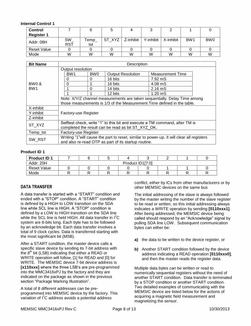
Internal Control 1
Control
Register 1
7 6 5 4 3 2 1 0
Addr: 08H SW_ RST
Temp_ tst
ST_XYZ Z-inhibit Y-inhibit X-inhibit BW1 BW0
Reset Value 0 0 0 0 0 0 0 0
Mode W W W W W W W W
Bit Name Description
BW0 & BW1
Output resolution
BW1 BW0 Output Resolution Measurement Time
0 0 16 bits 7.92 mS
0 1 16 bits 4.08 mS
1 0 14 bits 2.16 mS
1 1 12 bits 1.20 mS
Note: X/Y/Z channel measurements are taken sequentially. Delay Time among those measurements is 1/3 of the Measurement Time defined in the table.
X-inhibit
Factory-use Register Y-inhibit
Z-inhibit
ST_XYZ Selftest check, write “1” to this bit and execute a TM command, after TM is completed the result can be read as bit ST_XYZ_OK.
Temp_tst Factory-use Register
SW_RST Writing “1”will cause the part to reset, similar to power-up. It will clear all registers and also re-read OTP as part of its startup routine.
Product ID 1
Product ID 1 7 6 5 4 3 2 1 0
Addr: 20H Product ID1[7:0]
Reset Value 0 0 0 0 0 1 1 0
Mode R R R R R R R R
DATA TRANSFER
A data transfer is started with a “START” condition and ended with a “STOP” condition. A “START” condition is defined by a HIGH to LOW transition on the SDA line while SCL line is HIGH. A “STOP” condition is defined by a LOW to HIGH transition on the SDA line while the SCL line is held HIGH. All data transfer in I
2C
system are 8-bits long. Each byte has to be followed by an acknowledge bit. Each data transfer involves a total of 9 clock cycles. Data is transferred starting with the most significant bit (MSB).
After a START condition, the master device calls a specific slave device by sending its 7-bit address with the 8
th bit (LSB) indicating that either a READ or
WRITE operation will follow, [1] for READ and [0] for WRITE. The MEMSIC device 7-bit device address is
[x110xxx] where the three LSB’s are pre-programmed into the MMC3416xPJ by the factory and they are indicated on the package as shown in the previous section “Package Marking Illustration”.
A total of 8 different addresses can be pre-programmed into MEMSIC device by the factory. This variation of I
2C address avoids a potential address
conflict, either by ICs from other manufacturers or by other MEMSIC devices on the same bus
The initial addressing of the slave is always followed by the master writing the number of the slave register to be read or written, so this initial addressing always
indicates a WRITE operation by sending [0110xxx1]. After being addressed, the MEMSIC device being called should respond by an “Acknowledge” signal by pulling SDA line LOW. Subsequent communication bytes can either be:
a) the data to be written to the device register, or
b) Another START condition followed by the device
address indicating a READ operation [0110xxx0], and then the master reads the register data.
Multiple data bytes can be written or read to numerically sequential registers without the need of another START condition. Data transfer is terminated by a STOP condition or another START condition. Two detailed examples of communicating with the MEMSIC device are listed below for the actions of acquiring a magnetic field measurement and magnetizing the sensor.

MEMSIC MMC3416xPJ Rev C Page 9 of 13 10/30/2013
POWER STATE
MEMSIC MR Sensor will enter power down mode automatically after data acquisition is finished.
VDA VDD Power State
OFF(0 V) OFF(0V) OFF(0 V), no power consumption
OFF(0 V) 1.62~3.6 V OFF(0 V), power consumption is less than 1 uA.
1.62~3.6 V OFF(0 V) Power consumption is not predictable, not recommended state.
1.62~3.6 V 1.62~3.6 V
Normal operation mode, device will enter into power down mode automatically after data acquisition is finished
EXAMPLE MEASUREMENT
1st
cycle: A START condition is established by the Master Device followed by a call to the slave address [0110xxx] with the eighth bit held low to indicate a WRITE request. Note: [xxx] is determined by factory programming and a total of 8 different addresses are available.
2nd
cycle: After an acknowledge signal is received by the master device (MEMSIC device pulls SDA line low during 9
th SCL pulse), the master device sends the
address of Control Register 0 or [00000111] as the target register to be written. The MEMSIC device should acknowledge receipt of the address (9
th SCL
pulse, SCL pulled low).
3rd
cycle: The Master device writes to the Internal Control Register 0 the code [00000001] (TM high) to initiate data acquisition. The MEMSIC device should send an Acknowledge and internally initiate a measurement (collect x, y and z data). A STOP condition indicates the end of the write operation.
4th
cycle: The Master device sends a START command followed by the MEMSIC device’s seven bit address, and finally the eighth bit set low to indicate a WRITE. An Acknowledge should be send by the MEMSIC device in response.
5th
cycle: The Master device sends the MEMSIC device’s Status Register [00000110] as the address to read.
6th
cycle: The Master device sends a START command followed by the MEMSIC device’s seven bit address, and finally the eighth bit set high to indicate a READ. An Acknowledge should be send by the MEMSIC device in response.
7th
cycle: The Master device cycles the SCL line. This causes the Status Register data to appear on SDA line. Continuously read the Status Register until the
Meas Done bit (bit 0) is set to ‘1’. This indicates that data for the x, y, and z sensors is available to be read.
8th
cycle: The Master device sends a START command followed by the MEMSIC device’s seven bit address, and finally the eighth bit set low to indicate a WRITE. An Acknowledge should be send by the MEMSIC device in response.
9th
cycle: The Master device sends a [00000000] (Xout LSB register address) as the register address to read.
10th
cycle: The Master device calls the MEMSIC device’s address with a READ (8
th SCL cycle SDA line
high). An Acknowledge should be send by the MEMSIC device in response.
11th
cycle: Master device continues to cycle the SCL line, and each consecutive byte of data from the X, Y and Z registers should appear on the SDA line. The internal memory address pointer automatically moves to the next byte. The Master device acknowledges each. Thus:
12th
cycle: LSB of X channel.
13th
cycle: MSB of X channel.
14th
cycle: LSB of Y channel.
15th
cycle: MSB of Y channel.
16th
cycle: LSB of Z channel.
17th
cycle: MSB of Z channel.
Master ends communications by NOT sending an ‘Acknowledge’ and also follows with a ‘STOP’ command.
EXAMPLE OF SET
1st
cycle: A START condition is established by the Master Device followed by a call to the slave address [0110xxx] with the eighth bit held low to indicate a WRITE request. Note: [xxx] is determined by factory programming and a total of 8 different addresses are available.
2nd
cycle: After an acknowledge signal is received by the master device (The MEMSIC device pulls the SDA line low during the 9
th SCL pulse), the master device
sends [00000111] as the target address (Internal Control Register 0). The MEMSIC device should acknowledge receipt of the address (9
th SCL pulse).
3rd
cycle: The Master device writes to the MEMSIC device’s Internal Control Register 0 the code [10000000] (Refill Cap) to prepare for SET action.*
A minimum of 50ms wait should be provided to allow the MEMSIC device to finish its preparation for the SET action.
4th
cycle: The Master device writes to the MEMSIC device’s Internal Control 0 register the code

MEMSIC MMC3416xPJ Rev C Page 10 of 13 10/30/2013
[00100000] (SET bit) to initiate a SET action. The MEMSIC device should send an Acknowledge.
EXAMPLE OF RESET*
1st
cycle: A START condition is established by the Master Device followed by a call to the slave address [0110xxx] with the eighth bit held low to indicate a WRITE request. Note: [xxx] is determined by factory programming and a total of 8 different addresses are available.
2nd
cycle: After an acknowledge signal is received by the master device (The MEMSIC device pulls the SDA line low during the 9
th SCL pulse), the master device
sends [00000111] as the target address (Internal Control Register 0). The MEMSIC device should acknowledge receipt of the address (9
th SCL pulse).
3rd
cycle: The Master device writes to the MEMSIC device’s Internal Control Register 0 the code [10000000] (Refill Cap) to prepare for RESET action.
A minimum of 50ms wait should be provided to allow the MEMSIC device to finish its preparation for the RESET action.
4th
cycle: The Master device writes to the MEMSIC device’s Internal Control 0 register the code [01000000] (RESET bit) to initiate a RESET action. The MEMSIC device should send an Acknowledge.
At this point, the MEMSIC AMR sensors have been conditioned for optimum performance and data measurements can commence.
Note:
The RESET action can be skipped for most applications.
USING SET AND RESET TO REMOVE BRIDGE
OFFSET
The integrated SET and RESET functions of the MMC3416xPJ enables the user to remove the error associated with bridge Offset change as a function of temperature, thereby enabling more precise heading measurements over a wider temperature than competitive technologies. The SET and RESET functions effectively alternately flip the magnetic sensing polarity of the sensing elements of the device.
1) The most accurate magnetic field measurements can be obtained by using the protocol described as follows: Perform SET. This sets the internal magnetization of the sensing resistors in the direction of the SET field.
2) Perform MEASUREMENT. This measurement will contain not only the sensors response to the external magnetic field, H, but also the Offset; in other words,
Output1 = +H + Offset.
3) Perform RESET. This resets the internal magnetization of the sensing resistors in the direction of the RESET field, which is opposite to the SET field (180
o opposed).
4) Perform MEASUREMENT. This measurement will contain both the sensors response to the external field and also the Offset. In other words,
Output2 = -H + Offset. 5) Finally, calculate H by subtracting the two
measurements and dividing by 2. This procedure effectively eliminates the Offset from the measurement and therefore any changes in the Offset over temperature.
Note:
To calculate and store the offset add the two measurements and divide by 2. This calculated offset value can be subtracted from subsequent measurements to obtain H directly from each measurement.

MEMSIC MMC3416xPJ Rev C Page 11 of 13 10/30/2013
OPERATING TIMING
Operating Timing Diagram
Parameter Symbol Min. Typ. Max. Unit
Time to operate device after VDD valid top 10 mS
Time from Refill Cap to SET/RESET tRF 50 mS
Wait time to complete SET/RESET tSR 1 mS
Wait time to complete measurement
tTM BW=00 10 mS
tTM BW=01 5 mS
tTM BW=10 3 mS
tTM BW=11 1.5 mS
VDD
S T R T R T R S T R
tRF top
I2C
tSR tTM tSR
tTM tTM tTM
S
/
R
/
S
R
T
R
SET/RESET
Take Measurement
Read data
Repeat T & R
Wait the device to be ready for next operation

MEMSIC MMC3416xPJ Rev C Page 12 of 13 10/30/2013
STORAGE CONDITIONS Temperature: <30 ºC Humidity: <60%RH Period: 1 year (after delivery) Moisture Sensitivity Level: 3 Bake Prior to Reflow: storage period more than 1 year, or humidity indicator card reads >60% at 23±5 ºC Bake Procedure: refer to J-STD-033 Bake to Soldering: <1 week under 30 ºC, 60%RH condition
SOLDERING RECOMMENDATIONS
MEMSIC magnetic sensor is capable of withstanding an MSL3 / 260℃ solder reflow. Following is the reflow profile:
Note:
Reflow is limited by 2 times
The second reflow cycle should be applied after device has cooled down to 25 ºC (room temperature)
This is the reflow profile for Pb free process
The peak temperature on the sensor surface should be limited under 260 ºC for 10 seconds.
Solder paste’s reflow recommendation should be followed to get the best SMT quality.
If the part is mounted manually, please ensure the temperature could not exceed 260 ºC for 10 seconds.

MEMSIC MMC3416xPJ Rev C Page 13 of 13 10/30/2013
PACKAGE DRAWING (BGA package)
LAND PATTERN