magnetic field driven ambipolar quantum hall effect in
TRANSCRIPT
HAL Id: hal-01584484https://hal.archives-ouvertes.fr/hal-01584484
Submitted on 12 Jun 2019
HAL is a multi-disciplinary open accessarchive for the deposit and dissemination of sci-entific research documents, whether they are pub-lished or not. The documents may come fromteaching and research institutions in France orabroad, or from public or private research centers.
L’archive ouverte pluridisciplinaire HAL, estdestinée au dépôt et à la diffusion de documentsscientifiques de niveau recherche, publiés ou non,émanant des établissements d’enseignement et derecherche français ou étrangers, des laboratoirespublics ou privés.
Magnetic field driven ambipolar quantum Hall effect inepitaxial graphene close to the charge neutrality point
Abir Nachawaty, M. Yang, Wilfried Desrat, Sébastien Nanot, B. Jabakhanji,D. Kazazis, R. Yakimova, A. Cresti, Walter Escoffier, Benoit Jouault
To cite this version:Abir Nachawaty, M. Yang, Wilfried Desrat, Sébastien Nanot, B. Jabakhanji, et al.. Magnetic fielddriven ambipolar quantum Hall effect in epitaxial graphene close to the charge neutrality point. Physi-cal Review B: Condensed Matter and Materials Physics (1998-2015), American Physical Society, 2017,96 (7), pp.075442. �10.1103/PhysRevB.96.075442�. �hal-01584484�

PHYSICAL REVIEW B 96, 075442 (2017)
Magnetic field driven ambipolar quantum Hall effect in epitaxial grapheneclose to the charge neutrality point
A. Nachawaty,1,2 M. Yang,3 W. Desrat,1 S. Nanot,1 B. Jabakhanji,4 D. Kazazis,5,6 R. Yakimova,7
A. Cresti,8 W. Escoffier,3 and B. Jouault11Laboratoire Charles Coulomb (L2C), UMR 5221 CNRS-Université de Montpellier, F-Montpellier, France
2Laboratoire de Physique et Modélisation (LPM), EDST, Lebanese University, Tripoli, Lebanon3Laboratoire National des Champs Magnétiques Intenses (LNCMI-EMFL), UPR 3228, CNRS-UJF-UPS-INSA,
143 Avenue de Rangueil, 31400 Toulouse, France4College of Engineering and Technology, American University of the Middle East, Egaila, Kuwait
5Centre de Nanosciences et de Nanotechnologies, CNRS, Université Paris-Sud, Université Paris-Saclay,C2N Marcoussis, F-91460 Marcoussis, France
6Laboratory for Micro and Nanotechnology, Paul Scherrer Institute, CH-5232 Villigen-PSI, Switzerland7Department of Physics, Chemistry and Biology, Linköping University, SE-58183 Linköping, Sweden
8Univ. Grenoble Alpes, CNRS, Grenoble INP, IMEP-LaHC, F-38000 Grenoble, France(Received 6 July 2017; published 30 August 2017)
We have investigated the disorder of epitaxial graphene close to the charge neutrality point (CNP) by variousmethods: (i) at room temperature, by analyzing the dependence of the resistivity on the Hall coefficient; (ii) byfitting the temperature dependence of the Hall coefficient down to liquid helium temperature; (iii) by fitting themagnetoresistances at low temperature. All methods converge to give a disorder amplitude of (20 ± 10) meV.Because of this relatively low disorder, close to the CNP, at low temperature, the sample resistivity does notexhibit the standard value � h/4e2 but diverges. Moreover, the magnetoresistance curves have a unique ambipolarbehavior, which has been systematically observed for all studied samples. This is a signature of both asymmetry inthe density of states and in-plane charge transfer. The microscopic origin of this behavior cannot be unambiguouslydetermined. However, we propose a model in which the SiC substrate steps qualitatively explain the ambipolarbehavior.
DOI: 10.1103/PhysRevB.96.075442
I. INTRODUCTION
Undoubtedly, the best known exotic two-dimensional elec-tron system is graphene [1]. Among various exciting prop-erties, this material has demonstrated a half-integer quantumHall effect [2] (QHE) which is very robust in temperature [3],because of the extremely large energy separation between thefirst Landau levels (LL) lying close to the bottom of conductionand valence bands.
The QHE in graphene is strongly influenced by disorder andhence by the choice of the substrate. The quantum Hall plateausobserved in graphene on SiC (G/SiC) have a high breakdowncurrent [4] and appear at lower magnetic fields [5] with respectto graphene deposited on SiO2 [6]. The quantum plateaus inG/SiC devices are much larger in magnetic field than thoseobtained in graphene encapsulated in hBN [7], because theyare stabilized by charge transfer [8] and disorder [9]. Thanksto these properties, it was recently demonstrated that G/SiCcan act as a quantum electrical resistance standard [10], evenin experimental conditions relaxed with respect to the state ofthe art in GaAs-based quantum wells [11].
To date, fundamental and practical questions remain open.In particular, the fate of the G/SiC quantum plateaus close tothe charge neutrality point (CNP) has still to be elucidated.Achieving and controlling low doping is of primary interestto use graphene as a resistance standard at even lowermagnetic fields, or in cryogen-free systems [12]. G/SiC couldbe also a material of choice for testing theoretical modelspredicting additional quantum plateaus depending on the typeof disorder [13,14].
However, there exist only a few experimental analyses ofthe transport properties close to the CNP [5], mainly becauseG/SiC is intrinsically strongly n doped by the SiC substrate,thus requiring the system to be compensated by a top gate. Forgraphene on SiO2, close to the CNP, QHE reveals that electronsand holes coexist even when the energy spectrum is quantizedand the carriers partially localized [15,16], but for G/SiC eventhis rather intuitive picture has not been thoroughly tested.The amplitude of the disorder potential fluctuation has beenevaluated by various methods [5,17], but the type of disorderand its spatial and energy distribution close to the CNP remainmostly unknown.
In this paper, we present magnetotransport experiments inG/SiC to evaluate the disorder and to test the stability of theQHE close to the CNP. The results are largely unexpectedand reveal new physics in comparison to what is observedon other substrates. We show that not only electrons and holescoexist in high magnetic fields, but the carriers also redistributeunexpectedly as a function of magnetic field B, as illustratedin Fig. 1. In this figure, the graphene is tuned very closeto the CNP. The magnetoresistance reveals a magnetic fielddriven ambipolar QHE. At low B, a quantized p-like plateaustarts to develop. However, when B is increased further, thisplateau collapses and is replaced by a quantized n-like plateauof opposite sign. We show that this behavior is robust andreproducible for the range of doping where both types ofcarriers coexist and we propose a model based on disorderand in-plane charge transfer, after a detailed analysis of thesample disorder close to the CNP.
2469-9950/2017/96(7)/075442(7) 075442-1 ©2017 American Physical Society

A. NACHAWATY et al. PHYSICAL REVIEW B 96, 075442 (2017)
FIG. 1. Magnetoresistance observed in sample G31 at low tem-perature T = 1.7 K and low current I = 10 nA. A quantum Hallplateau at ρxy = RK/2 initially develops when B increases up to 0.5 T.At higher B, the Hall resistance changes sign and a long plateauappears at ρxy = RK/2. The longitudinal resistance ρxx shows apronounced maximum when the Hall resistance changes sign. ρxy < 0(> 0) corresponds to holes (electrons).
II. METHODS AND METHODOLOGY
A. Sample fabrication
The SiC/G samples have been grown epitaxially on theSi face of a semi-insulating 4H-SiC substrate at a hightemperature T = 2000◦C. The as-grown samples have largeuniform monolayer areas. Atomic force microscope analysisrevealed the presence of SiC steps, approximately 500-nmwide and 2-nm high, uniformly covered by the graphene layer.Additional Raman analysis revealed the presence of elongatedbilayer graphene patches, approximately 10-μm long and2-μm wide, covering around 5% of the total surface.
Hall bars of various size and geometry were then fabricatedby standard electron-beam lithography. The graphene wascovered by two layers of resist, as described in Ref. [18].The resist acts as a chemical gate and strongly reduces theintrinsic carrier density of the graphene layer.
Magnetotransport measurements were performed on fourSiC/G Hall bars, named G14, G31, G21, and G34. The barshave a length of 420 μm and a width of 100 μm, except forG34, which has a width of 20 μm.
B. Corona preparation
After the lithography process, the graphene layer wassystematically n doped with n � 6 × 1011 cm−2 at roomtemperature. Carrier density control was performed with ionprojections onto the resist bilayer covering graphene. Negativeions were produced by repeated corona discharges with a timeinterval of 17 s, following the method described in Ref. [19].The distance between the sample and the corona source was12 mm. Changes in the electronic properties of grapheneupon exposure to corona ions were detected by continuousmeasurements of the resistance and Hall coefficient KH atroom temperature, using low magnetic field (B = 0.05 T) anddc current I = ±1 μA. The evolution of the resistivity ρxx
as a function of the Hall coefficient KH during exposure toions is presented in Fig. 2. There is some point dispersiondue to the absence of correlation between the dischargesand the electrical measurements. However, the carrier densityclearly changes from its initial n doping of 6 × 1011 cm−2 toa p doping of 5 × 1011 cm−2 after a few hundreds cycles of
FIG. 2. ρxx vs KH during the corona preparation for sample G14.The initial state before the ion deposition is indicated by the bluefilled circle. The colored squares are various states from which theG14 sample has been cooled down at low temperature; see Fig. 4(a).The blue line is a fit without disorder (μe = μh = 4,300 cm2/Vs),and the black line a fit where the disorder is taken into account(s = 25 meV, μh = 2,750 cm2/Vs, μe/μh = 1.5).
corona discharge. After this point, additional ion projectionsare inefficient to increase further the p doping. When thedischarges are stopped, the carrier density drifts slowly towardsn doping and KH stabilizes around +1 k�/T within a fewhours. The initial carrier density is not recovered even whenthe sample is left several months under ambient atmosphere.
III. ESTIMATION OF DISORDER
A. Disorder estimated from KH (ρxx) at room temperature
To describe the sample evolution seen in Fig. 2, weuse the usual equations [20] that give the conduction ofa homogeneous sample, in which both electrons and holesparticipate in the conduction in parallel because of thermalactivation. The model is detailed in the appendix. The modeled(ρxx,KH ) curve is plotted for μe = μh = 4,300 cm2/Vs andT = 300 K as a blue solid line in Fig. 2(a) when μch spansthe energy window around the CNP. Here, μe, μh, and μch arethe electron mobility, hole mobility, and chemical potential,respectively. The model fits fairly well the data but with anobvious deviation on the hole side, where the KH coefficient isoverestimated. The asymmetry of the (ρxx,KH ) curve indicatesthat μe and μh differ. The data can be modeled more preciselyin two ways: (i) the mobility ratio μe/μh increases when thenumber of deposited ions increases because negative ions havea larger cross section for p-type charge carriers and theirpresence can decrease significantly the hole mobility [21];(ii) μe/μh > 1 and does not depend on the charge carrierconcentration but disorder has to be taken into account.
With the disorder amplitude s as an additional fitting param-eter, it is possible to fit the asymmetry of the ρxx(KH ) curve,as shown by the black line in Fig. 2. The fitting parameters
075442-2
MAGNETIC FIELD DRIVEN AMBIPOLAR QUANTUM HALL . . . PHYSICAL REVIEW B 96, 075442 (2017)
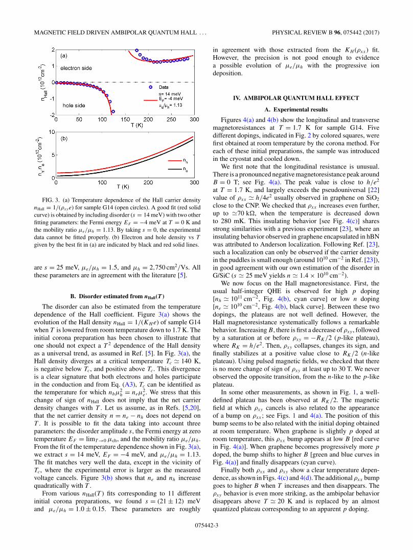
FIG. 3. (a) Temperature dependence of the Hall carrier densitynHall = 1/(ρxye) for sample G14 (open circles). A good fit (red solidcurve) is obtained by including disorder (s = 14 meV) with two otherfitting parameters: the Fermi energy EF = −4 meV at T = 0 K andthe mobility ratio μe/μh = 1.13. By taking s = 0, the experimentaldata cannot be fitted properly. (b) Electron and hole density vs T
given by the best fit in (a) are indicated by black and red solid lines.
are s = 25 meV, μe/μh = 1.5, and μh = 2,750 cm2/Vs. Allthese parameters are in agreement with the literature [5].
B. Disorder estimated from nHall(T )
The disorder can also be estimated from the temperaturedependence of the Hall coefficient. Figure 3(a) shows theevolution of the Hall density nHall = 1/(KHe) of sample G14when T is lowered from room temperature down to 1.7 K. Theinitial corona preparation has been chosen to illustrate thatone should not expect a T 2 dependence of the Hall densityas a universal trend, as assumed in Ref. [5]. In Fig. 3(a), theHall density diverges at a critical temperature Tc � 140 K,is negative below Tc, and positive above Tc. This divergenceis a clear signature that both electrons and holes participatein the conduction and from Eq. (A3), Tc can be identified asthe temperature for which nhμ
2h = neμ
2e . We stress that this
change of sign of nHall does not imply that the net carrierdensity changes with T . Let us assume, as in Refs. [5,20],that the net carrier density n = ne − nh does not depend onT . It is possible to fit the data taking into account threeparameters: the disorder amplitude s, the Fermi energy at zerotemperature EF = limT →0 μch, and the mobility ratio μe/μh.From the fit of the temperature dependence shown in Fig. 3(a),we extract s = 14 meV, EF = −4 meV, and μe/μh = 1.13.The fit matches very well the data, except in the vicinity ofTc, where the experimental error is larger as the measuredvoltage cancels. Figure 3(b) shows that ne and nh increasequadratically with T .
From various nHall(T ) fits corresponding to 11 differentinitial corona preparations, we found s = (21 ± 12) meVand μe/μh = 1.0 ± 0.15. These parameters are roughly
in agreement with those extracted from the KH (ρxx) fit.However, the precision is not good enough to evidencea possible evolution of μe/μh with the progressive iondeposition.
IV. AMBIPOLAR QUANTUM HALL EFFECT
A. Experimental results
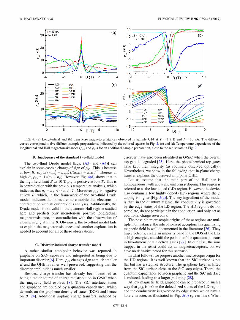
Figures 4(a) and 4(b) show the longitudinal and transversemagnetoresistances at T = 1.7 K for sample G14. Fivedifferent dopings, indicated in Fig. 2 by colored squares, werefirst obtained at room temperature by the corona method. Foreach of these initial preparations, the sample was introducedin the cryostat and cooled down.
We first note that the longitudinal resistance is unusual.There is a pronounced negative magnetoresistance peak aroundB = 0 T; see Fig. 4(a). The peak value is close to h/e2
at T = 1.7 K, and largely exceeds the pseudouniversal [22]value of ρxx � h/4e2 usually observed in graphene on SiO2
close to the CNP. We checked that ρxx increases even further,up to �70 k�, when the temperature is decreased downto 280 mK. This insulating behavior [see Fig. 4(c)] sharesstrong similarities with a previous experiment [23], where aninsulating behavior observed in graphene encapsulated in hBNwas attributed to Anderson localization. Following Ref. [23],such a localization can only be observed if the carrier densityin the puddles is small enough (around 1010 cm−2 in Ref. [23]),in good agreement with our own estimation of the disorder inG/SiC (s � 25 meV yields n � 1.4 × 1010 cm−2).
We now focus on the Hall magnetoresistance. First, theusual half-integer QHE is observed for high p doping[nh � 1011 cm−2, Fig. 4(b), cyan curve] or low n doping[ne � 1010 cm−2, Fig. 4(b), black curve]. Between these twodopings, the plateaus are not well defined. However, theHall magnetoresistance systematically follows a remarkablebehavior. Increasing B, there is first a decrease of ρxy , followedby a saturation at or before ρxy = −RK/2 (p-like plateau),where RK = h/e2. Then, ρxy collapses, changes its sign, andfinally stabilizes at a positive value close to RK/2 (n-likeplateau). Using pulsed magnetic fields, we checked that thereis no more change of sign of ρxy at least up to 30 T. We neverobserved the opposite transition, from the n-like to the p-likeplateau.
In some other measurements, as shown in Fig. 1, a well-defined plateau has been observed at RK/2. The magneticfield at which ρxy cancels is also related to the appearanceof a bump on ρxx ; see Figs. 1 and 4(a). The position of thisbump seems to be also related with the initial doping obtainedat room temperature. When graphene is slightly p doped atroom temperature, this ρxx bump appears at low B [red curvein Fig. 4(a)]. When graphene becomes progressively more p
doped, the bump shifts to higher B [green and blue curves inFig. 4(a)] and finally disappears (cyan curve).
Finally both ρxx and ρxy show a clear temperature depen-dence, as shown in Figs. 4(c) and 4(d). The additional ρxx bumpgoes to higher B when T increases and then disappears. Theρxy behavior is even more striking, as the ambipolar behaviordisappears above T � 20 K and is replaced by an almostquantized plateau corresponding to an apparent p doping.
075442-3
A. NACHAWATY et al. PHYSICAL REVIEW B 96, 075442 (2017)
FIG. 4. (a) Longitudinal and (b) transverse magnetoresistances observed in sample G14 at T = 1.7 K and I = 10 nA. The differentcurves correspond to five different sample preparations, indicated by the colored squares in Fig. 2. (c) and (d) Temperature dependence of thelongitudinal and Hall magnetoresistances (ρxx and ρxy) for an additional sample preparation, close to the red square in Fig. 2.
B. Inadequacy of the standard two-fluid model
The two-fluid Drude model [Eqs. (A3) and (A4)] canexplain in some cases a change of sign of ρxy . This is becauseat low B, ρxy � (neμ
2e − nhμ
2h)/(nhμh + neμe)2 whereas at
high B, ρxy � 1/(ne − nh). However, Fig. 4(d) shows that inthe high field limit B � 10 T, ρxy is positive at low T . This isin contradiction with the previous temperature analysis, whichindicates that ne − nh < 0 at all T . Moreover ρxy is negativeat low B, which, in the framework of the two-fluid Drudemodel, indicates that holes are more mobile than electrons, incontradiction with all our previous analyses. Additionally, theDrude model is not valid in the quantum Hall regime studiedhere and predicts only monotonous positive longitudinalmagnetoresistance, in contradiction with the observation ofa bump in ρxx at finite B. Obviously, the two-fluid model failsto explain the magnetoresistances and another explanation isneeded to account for all of these observations.
C. Disorder-induced charge transfer model
A rather similar ambipolar behavior was reported ingraphene on SiO2 substrate and interpreted as being due toimportant disorder [6]. Here, ρxy changes sign at much smallerB and the QHE is rather well preserved, suggesting that thedisorder amplitude is much smaller.
Besides, charge transfer has already been identified asbeing a major source of charge redistribution in G/SiC whenthe magnetic field evolves [8]. The SiC interface statesand graphene are coupled by a quantum capacitance, whichdepends on the graphene density of states (DOS) and henceon B [24]. Additional in-plane charge transfers, induced by
disorder, have also been identified in G/SiC when the overalltop gate is degraded [25]. Here, the photochemical top gateshave kept their integrity (as routinely observed optically).Nevertheless, we show in the following that in-plane chargetransfer explains the observed ambipolar QHE.
Let us assume that the main part of the Hall bar ishomogeneous, with a low and uniform p doping. This region isreferred to as the low doped (LD) region. However, the devicealso contains a few highly doped (HD) regions where the p
doping is higher [Fig. 5(a)]. The key ingredient of the modelis that, in the quantum regime, the conductivity is governedby the edge states of the LD region. The HD regions do notpercolate, do not participate in the conduction, and only act asadditional charge reservoirs.
The possible microscopic origins of these regions are mul-tiple. For instance, the role of ionized acceptors in a quantizingmagnetic field is well documented in the literature [26]. Theytrap electrons, create an impurity band in the DOS of the LLsat high energies, and shift the position of the quantum plateausin two-dimensional electron gases [27]. In our case, the ionstrapped in the resist could act as magnetoacceptors, but wehave no definitive proof for this scenario.
In what follows, we propose another microscopic origin forthe HD regions. It is well known that the SiC surface is notflat but has a steplike structure. The graphene layer is liftedfrom the SiC surface close to the SiC step edges. There, thequantum capacitance between graphene and the SiC interfaceis reduced, leading to a larger p doping [28].
At low magnetic field, graphene can be prepared in such away that μch is below the delocalized states of the LD regionand the conductivity is governed by edge states which have ahole character, as illustrated in Fig. 5(b) (green line). When
075442-4

MAGNETIC FIELD DRIVEN AMBIPOLAR QUANTUM HALL . . . PHYSICAL REVIEW B 96, 075442 (2017)
FIG. 5. (a) Top-view sketch of the Hall bar, embedding regions(HD, orange color) whose CNP is at higher energy than thesurrounding graphene region (LD, blue color). The edge states ofthe devices are also presented as dark blue lines. (b) Profile of theLL near the CNP. The LD and HD regions are indicated by blue andorange lines, respectively. The LL splits at the sample edges. WhenB increases, the electrochemical potential tries to maintain a constanttotal charge and may cross the CNP of the LD region at a finite B. (c)Estimated carrier density nLD in the LD region vs B, for the modelgiven in the main text, μLD
CNP = 14 meV, � = 15 meV, α = 30%.
the magnetic field is increased, the LL degeneracy increases.As the total net carrier density (including LD and HD regions)tends to remain constant, μch moves to higher energy (redline). When the magnetic field is high enough, μch has shiftedbetween the LL energies of the LD and HD regions. There, theLD region has become n doped whereas the HD puddles arestill p doped. The conductivity is then governed by the LD edgestates which have now an electron character. Experimentally,the magnetic field at which ρxy reverses can be as low asBm = 0.5 T, which gives the minimal size of the HD regions:√
h̄/eBm � 40 nm.Below we derive numerical estimates for this model
assuming that the inhomogeneity comes from the steplikestructure. First, because of the quantum capacitance takingplace between states at the G/SiC interface and graphene [24],any modification of the DOS structure due to the magneticfield induces charge displacement. For each region LD andHD, the balance equation gives
ni(μch) = −ng + βi(A + μi
CNP − μch), (1)
where i labels the LD and HD regions, ng is the gatecharge density, A is the work-function difference betweenundoped graphene and the interface states, βi is an effectivedensity of states, and μi
CNP is the potential of the CNP in
region i. We choose μLDCNP = 0 as a reference. βi is given
by βi = ε0/(ε0 + e2diγ ) where ε0 is the vacuum dielectricconstant, γ is the density of interface states, and di is thedistance between graphene and the interface.
At equilibrium, the electrochemical potential is the same inthe whole sample. Following Ref. [25], the equation to solve isthen obtained by summing the contributions of nHD and nLD:
(1 − α)nLD(μch) + αnHD(μch)
= − ng + (1 − α)βLD(A − μch)
+αβHD(A + μHD
CNP − μch), (2)
where α is the proportion of the HD region. On the left side ofthis equation, both nLD and nHD can be numerically estimatedat a given magnetic field, where the DOS is given by a sum ofLandau levels, each with a fixed Gaussian broadening �. Thechosen parameters are ng = 1.59 × 1010 cm−2, A = 0.4 eV,γ = 5 × 1012 cm−2eV−1, and � = 15 meV. They have beenchosen in accordance with the literature [8].
We assume that the LD and HD regions only differ by avery small difference between dLD and dHD: dLD = 0.3 nm anddHD = 0.4 nm. This small difference induces a shift betweenthe CNPs of the two LD and HD regions which is comparableto our estimation of the disorder: μHD
CNP = 14 meV � s.Figure 5(c) shows nLD(B) obtained from solving Eq. (2),
with α = 30%. As the model assumes that the conductionis governed by the LD region alone, the magnetic fielddependence of nLD(B) reproduces the ambipolar behaviorof the transverse magnetoresistance. Note that a qualitativeagreement of the T dependence is also obtained. At low B,nLD remains essentially T independent, in agreement with theprevious nHall(T ) analyses. By contrast, the critical magneticfield at which the sign of ρxy (i.e., the sign of nLD) reversesis shifted to higher B when T increases. Experimentally thistrend is indeed observed, with a shift which is even morepronounced, suggesting that some other parameters (e.g., A orγ ) could also be T dependent.
Finally, this model relates unambiguously the ρxx bump tothe conduction through the delocalized states of the LD region.The model also predicts that this bump shifts to higher B
when the initial p doping increases, as indeed experimentallyobserved.
V. CONCLUSION
To conclude, we have investigated the disorder of epitaxialgraphene close to the charge neutrality point by various analy-ses of the transport properties. All these analyses converge togive a disorder amplitude of the order of a few tens of meV.Remarkably, the magnetoresistance curves have an ambipolarbehavior driven by the magnetic field. We interpret this as thesignature of a very specific disorder combined with in-planecharge transfer between different regions in the graphene layer.The origin of disorder cannot be unambiguously determined.Nevertheless we propose a model with numerical estimationsshowing that the magnetic field behavior could be related tothe stepped SiC substrate.
075442-5

A. NACHAWATY et al. PHYSICAL REVIEW B 96, 075442 (2017)
ACKNOWLEDGMENTS
We thank F. Schopfer and W. Poirier (Laboratoire Nationalde Métrologie et d’Essais, France) for fruitful discussion.This work has been supported in part by the French AgenceNationale pour la Recherche (Grant No. ANR-16-CE09-0016) and by Programme Investissements d’Avenir under theprogram ANR-11-IDEX-0002-02, reference ANR-10-LABX-0037-NEXT. Part of this work was performed at LNCMI underEMFL Proposal No. TSC06-116.
APPENDIX: MODEL OF DISORDER
To describe the sample evolution seen in Fig. 2, wereproduce below the usual equations [20] that give theconduction of a homogeneous sample, in which both electronsand holes participate in the conduction in parallel because ofthermal activation. The total electron density is given by
ne =∫ ∞
−∞De(E)f (E − μch)dE, (A1)
where De(E) = D1Eθ (E) is the density of states(DOS) for electrons, D1 = gsgv/(2πh̄2v2
F ), gs = 2 andgv = 2 are the spin and valley degeneracies, f =1/[1 + exp((E − μch)/kBT )] is the Fermi distribution func-tion, θ is the Heavyside function, and μch is the chemical
potential. The total hole density is given by
nh =∫ ∞
−∞Dh(E)(1 − f (E − μch))dE, (A2)
where Dh(E) = De(−E) is the DOS for holes. At lowmagnetic fields μeB,μhB � 1, the Hall and longitudinalresistivities are given by
ρxy = −ρyx = −1
e
(nhμ
2h − neμ
2e
) + μ2hμ
2eB
2(nh − ne)
(nhμh + neμe)2 + μ2hμ
2e(nh − ne)2B2
B,
(A3)
and
ρxx = 1
e
nhμh + neμe + (neμeμ
2h + nhμhμ
2e
)B2
(nhμh + neμe)2 + μ2hμ
2e(nh − ne)2B2
, (A4)
where μe and μh are the electron and hole mobility, respec-tively, and −e is the electron charge.
In the limit B → 0, the above equations (A3) and (A4) giveρxx and KH = limB→0 ρxy/B as functions of the parametersμch, μe, μh, and T .
To explore the role of disorder, we introduce the probabilityP (V )dV of finding the local electronic potential within a rangedV about V . The disorder is assumed to have a Gaussian form:P (V ) = 1/
√2πs2 exp(−V 2/2s2). The disordered electronic
DOS is then given by De(E) = ∫ E
−∞ D1(E − V )P (V )dV . Asimilar formula holds for Dh.
[1] A. K. Geim and K. S. Novoselov, Nat. Mater. 6, 183(2007).
[2] Y. Zhang, Y.-W. Tan, H. L. Stormer, and P. Kim, Nature (London)438, 201 (2005).
[3] K. S. Novoselov, Z. Jiang, Y. Zhang, S. V. Morozov, H. L.Stormer, U. Zeitler, J. C. Maan, G. S. Boebinger, P. Kim, andA. K. Geim, Science 315, 1379 (2007).
[4] J. A. Alexander-Webber, A. M. R. Baker, T. J. B. M. Janssen,A. Tzalenchuk, S. Lara-Avila, S. Kubatkin, R. Yakimova, B. A.Piot, D. K. Maude, and R. J. Nicholas, Phys. Rev. Lett. 111,096601 (2013).
[5] J. Huang, J. Alexander-Webber, A. Baker, T. Janssen, A.Tzalenchuk, V. Antonov, T. Yager, S. Lara-Avila, S. Kubatkin,R. Yakimova et al., Phys. Rev. B 92, 075407 (2015).
[6] J.-M. Poumirol, W. Escoffier, A. Kumar, B. Raquet, and M.Goiran, Phys. Rev. B 82, 121401 (2010).
[7] C. Dean, A. Young, P. Cadden-Zimansky, L. Wang, H. Ren, K.Watanabe, T. Taniguchi, P. Kim, J. Hone, and K. Shepard, Nat.Phys. 7, 693 (2011).
[8] T. J. B. M. Janssen, A. Tzalenchuk, R. Yakimova, S. Kubatkin,S. Lara-Avila, S. Kopylov, and V. I. Fal’ko, Phys. Rev. B 83,233402 (2011).
[9] F. Lafont, R. Ribeiro-Palau, D. Kazazis, A. Michon, O. Coutu-raud, C. Consejo, T. Chassagne, M. Zielinski, M. Portail, B.Jouault et al., Nat. Commun. 6, 6806 (2015).
[10] A. Tzalenchuk, S. Lara-Avila, A. Kalaboukhov, S. Paolillo, M.Syväjärvi, R. Yakimova, O. Kazakova, T. Janssen, V. Fal’ko,and S. Kubatkin, Nat. Nanotechnol. 5, 186 (2010).
[11] R. Ribeiro-Palau, F. Lafont, J. Brun-Picard, D. Kazazis,A. Michon, F. Cheynis, O. Couturaud, C. Consejo, B. Jouault,W. Poirier et al., Nat. Nanotechnol. 10, 965 (2015).
[12] T. J. B. M. Janssen, S. Rozhko, I. Antonov, A. Tzalenchuk, J. M.Williams, Z. Melhem, H. He, S. Lara-Avila, S. Kubatkin, andR. Yakimova, 2D Materials 2, 035015 (2015).
[13] K. Nomura, S. Ryu, M. Koshino, C. Mudry, and A. Furusaki,Phys. Rev. Lett. 100, 246806 (2008).
[14] P. M. Ostrovsky, I. V. Gornyi, and A. D. Mirlin, Phys. Rev. B77, 195430 (2008).
[15] S. Wiedmann, H. van Elferen, E. Kurganova, M. Katsnel-son, A. Giesbers, A. Veligura, B. van Wees, R. Gorbachev,K. Novoselov, J. Maan et al., Phys. Rev. B 84, 115314(2011).
[16] E. V. Kurganova, S. Wiedmann, A. J. M. Giesbers, R. V.Gorbachev, K. S. Novoselov, M. I. Katsnelson, T. Tudorovskiy,J. C. Maan, and U. Zeitler, Phys. Rev. B 87, 085447(2013).
[17] A. Curtin, M. Fuhrer, J. Tedesco, R. Myers-Ward, C. Eddy, Jr.,and D. Gaskill, Appl. Phys. Lett. 98, 243111 (2011).
[18] S. Lara-Avila, K. Moth-Poulsen, R. Yakimova, T. Bjørnholm,V. Fal’ko, A. Tzalenchuk, and S. Kubatkin, Adv. Mater. 23, 878(2011).
[19] A. Lartsev, T. Yager, T. Bergsten, A. Tzalenchuk, T. J. B. M.Janssen, R. Yakimova, S. Lara-Avila, and S. Kubatkin, Appl.Phys. Lett. 105, 063106 (2014).
[20] Q. Li, E. H. Hwang, and S. Das Sarma, Phys. Rev. B 84, 115442(2011).
075442-6
MAGNETIC FIELD DRIVEN AMBIPOLAR QUANTUM HALL . . . PHYSICAL REVIEW B 96, 075442 (2017)
[21] D. Novikov, Appl. Phys. Lett. 91, 102102 (2007).[22] S. Adam, E. H. Hwang, V. M. Galitski, and S. Das Sarma, Proc.
Natl. Acad. Sci. USA 104, 18392 (2007).[23] L. Ponomarenko, A. K. Geim, A. A. Zhukov, R. Jalil, S.
V. Morozov, K. S. Novoselov, I. V. Grigorieva, E. H. Hill,V. V. Cheianov, V. I. Fal’ko et al., Nat. Phys. 7, 958(2011).
[24] S. Kopylov, A. Tzalenchuk, S. Kubatkin, and V. I. Fal’ko, Appl.Phys. Lett. 97, 112109 (2010).
[25] M. Yang, O. Couturaud, W. Desrat, C. Consejo, D. Kazazis, R.Yakimova, M. Syväjärvi, M. Goiran, J. Béard, P. Frings et al.,Phys. Rev. Lett. 117, 237702 (2016).
[26] M. Kubisa and W. Zawadzki, Semicond. Sci. Technol. 11, 1263(1996).
[27] R. Haug, R. Gerhardts, K. v. Klitzing, and K. Ploog, Phys. Rev.Lett. 59, 1349 (1987).
[28] T. Low, V. Perebeinos, J. Tersoff, and P. Avouris, Phys. Rev.Lett. 108, 096601 (2012).
075442-7