macgdi: low power mac based filter bank using gdi … gdi logic for hearing aid applications . ......
TRANSCRIPT

MACGDI: Low Power MAC Based Filter Bank
Using GDI Logic for Hearing Aid Applications
N. Subbulakshmi Sri Ramakrishna Engineering College, Coimbatore, India
Email: [email protected]
R. Manimegalai Park College of Technology, Coimbatore, India
Email: [email protected]
Abstract—An electronic hearing aid is a small device which
is located in and around the human ear to enhance the
hearing ability. It is used to compensate the hearing loss and
enhance the quality of sound for hearing impaired people.
Hearing aid device in signal processing is an important field
of research for the last three decades. Recently, power
aware hearing aid device designs with smaller footprint,
gain considerable importance. The hearing aid device has
been designed for portable communication equipment with
digital filtering, speech processing, sub-band coding and
speech enhancement. With the technological advancements
in the Digital Signal Processing (DSP) algorithms, design of
hearing aid devices has been improved continuously. It is
expected that more innovations in hearing aid device
technology will be released in future, with new
developments in signal processing algorithms and filter
bank designs. Finite Impulse Response (FIR) filter design is
very important and crucial for signal processing algorithms.
The focus of the designer is on minimization of power on the
domain of digital circuit for battery operated devices. In this
paper, Gated Diffusion Input (GDI) logic is used in the
proposed Filter Bank design in order to minimize power.
The Multiply-Accumulate (MAC) unit of the proposed filter
bank is designed by GDI logic and modified GDI logic. GDI
logic has three terminals which are Common Gate (G),
PMOS (P), NMOS (N) and output terminal. The number of
transistors is reduced in GDI when compared to
Complementary Metal Oxide Semiconductor (CMOS) logic
due to reduced switching activity. This paper briefly
describes the basic functions of power and delay of GDI
logic and modified GDI logic. The proposed modified GDI
logic provides better results in area and power when
compared to CMOS logic.
Index Terms—filter bank, digital hearing aid, DSP
algorithms, multiply accumulate unit
I. INTRODUCTION
With the advanced technology and an increasing trend
towards portable computing and wireless communication,
low power designs have gained importance. Finite
Impulse Response (FIR) filtering is one of the most
commonly used DSP functions. It is achieved by
Manuscript received February 16, 2017; revised June 28, 2017.
convolving the input data samples with the desired unit
impulse response of the filter. The front end of a typical
hearing aid device consists of two microphones for noise
suppression. First microphone contains speech and noise.
The other is for producing reference signal which is
passed through a filter. Then, it is subtracted from the
delayed version of the input signal. Fig. 1 shows the
block diagram of a MAC based filter which includes Data
memory, Coefficient memory, MAC unit, output register
and a control unit [1]. Data memory provides data
samples to the filter bank. The co-efficient memory has
fixed values.
Modified Gate Diffusion Input logic is much more
power-efficient than Gate Diffusion Input (GDI) logic
and CMOS logic design. DC and Transient analysis are
performed on modified GDI logic circuit designs and a
wider range of different logic cells. The use of practical
circuit realizations reveal modified GDI is advantageous
over GDI and CMOS in majority of the cases with
respect to speed, area and power dissipation.
Rest of the paper is organized as follows: Section II
presents the Folded Direct Form (FDF) structure. Section
III presents details of CMOS, GDI and Modified GDI
logic styles. Section IV focuses on the proposed MAC
based Filter bank using GDI for hearing aid devices.
Section V presents the experimental results obtained
using the proposed MAC based filter bank design by
employing GDI logic. Finally, Section VI concludes the
paper.
II. FDF FILTER STRUCTURE
A linear phase FIR filter is implemented using Direct
Form (DF) structure or a Folded Direct Form (FDF)
structure. The filter bank design proposed in this paper
uses FDF structure along with MAC. The FDF structure
minimizes the number of multiplications by half at the
expense of additional hardware with the help of Dual
Edge Triggered (DET) Flip-flop which is described in [1].
The FDF structure is shown in Fig. 2. The block has two
separate memories for program and data, that can be
accessed at the same time. One of the memories can be
used to store coefficients in Read Only Memory (ROM)
and the other to store input data samples in Random
International Journal of Electronics and Electrical Engineering Vol. 5, No. 3, June 2017
©2017 Int. J. Electron. Electr. Eng. 235doi: 10.18178/ijeee.5.3.235-239

Access Memory (RAM). A dual-port memory and an
additional adder would be required to access two data
samples at a time and to add them prior to the
multiplication stage. The arithmetic block performs fixed-
point computation on numbers which represent in 2’s
complement form.
The proposed filter structure includes a multiplier and
an adder / subtractor connected to the accumulator so as
to be proficiently perform the Multiply-Accumulate
(MAC) operation. After adding two data samples the
resultant is converted into Sign Magnitude representation.
Then, the output is multiplied with the corresponding co-
efficient. After that the multiplied value is again
transformed to 2’s complement form for further
processing. The output is added with the accumulator
value and then it is taken as final output i.e. data output.
After every computation a new data sample is read and
stored in the output memory. In order to get the new data
sample, the existing data samples need to be shifted by
one position for every output. This operation is done by
MAC unit.
III. LOGIC STYLES: CMOS, GDI AND MODIFIED GDI
LOGIC
Many logic styles have been introduced in the DSP
algorithms such as (i) Complementary Metal Oxide
Semiconductor (CMOS) (ii) Transmission Gates (iii)
Complementary Pass Transistor logic (iv) Double Pass
Transistor logic (v) Swing Restored Pass Transistor (vi)
Power saved Pass Transistor. Transmission Gates are used
to realize complex functions with minimum number of
complementary transistors. Pass Transistor Logic (PTL) is
a method to achieve minimum number of transistors in the
design. But PTL has the disadvantage of having low speed
in smaller circuits. In this section, CMOS, GDI and
modified GDI logic styles are presented and compared
with many functions.
A. CMOS
Complementary Metal Oxide Semiconductor (CMOS)
is a logic style for designing integrated circuits. CMOS is
constructed by combining a PMOS transistor which has
strong 1 and an NMOS transistor which has strong 0. The
PMOS transistors are getting input from the voltage
source (VDD). Similarly, the NMOS transistors are
getting an input from the ground (GND). A PMOS
transistor contains low resistance between its source and
drain contacts when a low gate voltage is given and high
resistance when a high gate voltage is applied. However,
an NMOS transistor produces high resistance between
source and drain when a low gate voltage is applied and
low resistance when a high gate voltage is applied.
A logic AND gate is a category of digital logic gate. In
CMOS logic, AND gate is designed using six transistors
which include three PMOS transistors and three NMOS
transistors. The Boolean function for an AND gate is set
as (A.B = D). The above expression has two inputs A and
B and the output is D. If inputs A and B are low, the
output D will be low. If A input is low and B input is
high, the output D will be low. If input A is high and
input B is low, the output D will be low. If both A and B
inputs are high, the output D will be high. CMOS XOR
gate comprises of two inverters and two transmission
gates. The inverter produces reverse value of the input i.e.
0 to 1 and vice versa. The transmission gate produces the
output depends on the input applied. For XOR gate the
Boolean function is D= A'B+AB', consider two inputs A
and B in the design of CMOS logic: if both the inputs A
and B are low, the output D will be low. If both the inputs
A and B are high, the output D will be low. If one of the
inputs is high and other input is low, the output D will be
high.
Multiplexer (MUX) is designed with the help of a
control signal which is also called as a select signal. It
selects one of the input signals and that input signal is
forwarded into a output line. A multiplexer is a ratio of
2n:n, where 2
n represents the number of inputs and n
represents the number of outputs. MUX consists of 12
transistors in the CMOS logic. It has six PMOS and six
NMOS transistors. MUX output depends on the selection
signals. Consider 2×1 Multiplexer which has 2 inputs and
1 output and it has 1 selection line. Consider, if selection
line is high, it selects input A and if selection line is low
it selects input B.
B. GDI
Gated Diffusion Input (GDI) logic is a basic cell [2], [3]
with four terminals as shown in Fig. 3. Table I shows that
the basic logic functions using GDI logic. The GDI logic
International Journal of Electronics and Electrical Engineering Vol. 5, No. 3, June 2017
©2017 Int. J. Electron. Electr. Eng. 236
Figure 1. Block diagram of MAC based filter structure
Figure. 2 FDF structure

International Journal of Electronics and Electrical Engineering Vol. 5, No. 3, June 2017
©2017 Int. J. Electron. Electr. Eng. 237
cell has some important differences when compared to
CMOS logic inverter.
Gated Diffusion Input (GDI) includes three
terminals as inputs: (i) Gate (G) which is common
for both PMOS and NMOS (ii) the input of PMOS
for source / drain (iii) the input of NMOS for
source and drain.
Sources of both PMOS and NMOS are not
connected to supply voltage (VDD) and ground
(GND) respectively.
Bulk of PMOS in a GDI cell is connected with P
and Bulk of NMOS is connected with N.
Figure 3. Basic GDI cell [3]
TABLE I. BASIC LOGIC FUNCTIONS USING GDI
PMOS
P
NMOS
N
GATE
GOUTPUT D
FUNCTIONS
1 0 A A' Inverter
B 0 A A'B Function1
1 B A A'+B Function2
B 1 A A+B OR
0 B A AB AND
B C A A'B+AC MULTIPLEXER
B B' A A'B+AC' XOR
B' B A A'B'+AC XNOR
Table II presents number of transistors.
TABLE II. NUMBER OF TRANSISTORS
Function CMOS GDI
Inverter 2 2
Function1 6 2
Function2 6 2
OR 6 2
AND 6 2
MUX 12 2
XOR 16 4
XNOR 16 4
NAND 4 4
NOR 4 4
C. Modified GDI
In Modified GDI technique, PMOS substrate terminal
(Psub) is connected to the supply voltage and NMOS
substrate terminal (Nsub) is connected to the ground.
Modified GDI cell can be configured with all current
CMOS technologies. Table III shows various logic
functions that can be implemented using modified GDI.
Fig. 4 shows the basic cell structure of modified GDI
logic [3].
Figure 4. Basic modified GDI cell [3]
TABLE III. FUNCTIONS OF MODIFIED GDI
N Nsub P Psub G OutputD
Functions
0 0 1 1 A A' Inverter
A A 0 A B AB AND
1 0 A D B A+B OR
A' 0 A 1 B A'B+AB' XOR
A 0 A' 1 B AB+A'B' XNOR
Table IV represents the switching delay and average
power of various logic functions such as AND, OR,
NAND, NOR and XOR using GDI, modified GDI and
CMOS logic styles. Observing the table values, the
modified GDI logic achieves comparatively less power
and minimum switching delay than GDI and CMOS logic.
Low power optimization techniques have been discussed
in many papers [4], [5], [6] and [7]. The full swing GDI
technique is discussed in [8]-[11].
TABLE IV. COMPARISONS BASED ON DELAY AND POWER
Functions
GDI Modified GDI CMOS
Delay
(ps)
Power
(μW)
Delay
(ps)
Power
(μW)
Delay
(ps)
Power
(μW)
AND 0.2 1.286 0.18 0.986 0.24 1.698
OR 0.28 1.3 0.18 1.2 0.27 1.550
NAND 0.52 0.657 0.242 0.54 0.28 0.604
NOR 0.54 0.68 0.28 0.654 0.3 0.756
XOR 0.545 1.48 0.362 1.23 0.567 1.5
IV. PROPOSED MAC BASED FILTER BANK FOR
DIGITAL HEARING AIDS
This paper proposes a MAC based filter bank using
GDI and modified GDI logic styles (MACGDI). MAC
Unit pays attention to many of the Digital Signal
Processing (DSP) Applications. Relating to
multiplication- Accumulation (MAC) unit is designed for
best performance in digital signal processing systems.
Some of the algorithms are basically accomplished by
repetitive application of multiplication and addition.
International Journal of Electronics and Electrical Engineering Vol. 5, No. 3, June 2017
©2017 Int. J. Electron. Electr. Eng. 238
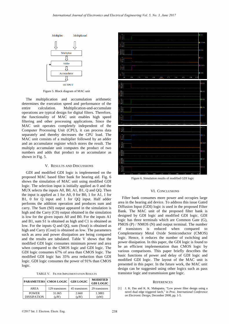
Figure 5. Block diagram of MAC unit
The multiplication and accumulation arithmetic
determines the execution speed and performance of the
entire calculation. Multiplication-and-accumulate
operations are typical design for digital filters. Therefore,
the functionality of MAC unit enables high speed
filtering and other processing applications. Since the
MAC unit operates completely independent of the
Computer Processing Unit (CPU), it can process data
separately and thereby decreases the CPU load. The
MAC unit consists of a multiplier followed by an adder
and an accumulator register which stores the result. The
multiply accumulate unit computes the product of two
numbers and adds that product to an accumulator as
shown in Fig. 5.
V. RESULTS AND DISCUSSIONS
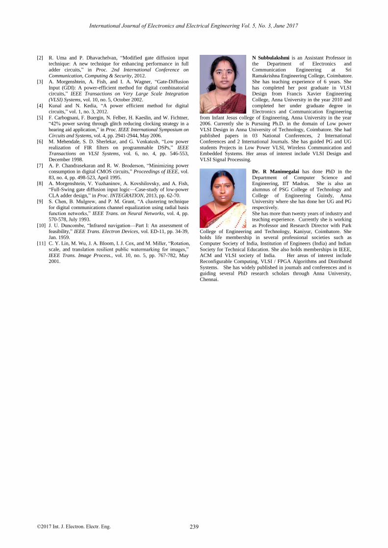
GDI and modified GDI logic is implemented on the
proposed MAC based filter bank for hearing aid. Fig. 6
shows the simulation of MAC unit using modified GDI
logic. The selection input is initially applied as 0 and the
MUX selects the inputs A0, B0, A1, B1, Q and QQ. Then
the input is applied as 1 for A0, 0 for B0, 1 for A1, 1 for
B1, 0 for Q input and 1 for QQ input. Half adder
performs the addition operation and produces sum and
carry. The Sum (S0) output appeared in the simulation is
high and the Carry (C0) output obtained in the simulation
is low for the given inputs A0 and B0. For the inputs A1
and B1, sum S1 is obtained as high and C1 is obtained as
low. For the inputs Q and QQ, sum (Sout) is obtained as
high and Carry (Cout) is obtained as low. The parameters
such as area and power dissipation are being compared
and the results are tabulated. Table V shows that the
modified GDI logic consumes minimum power and area
when compared to the CMOS logic and GDI logic. The
GDI logic consumes 67% of area than CMOS logic. The
modified GDI logic has 35% area reduction than GDI
logic. GDI logic consumes the power of 91% than CMOS
logic.
TABLE V. FILTER IMPLEMENTATION RESULTS
PARAMETERS CMOS LOGIC GDI LOGIC MODIFIED
GDI LOGIC
AREA 129 transistors 45 transistors 29 transistors
POWER
DISSIPATION
31.065
(μW)
2.660
(μW)
1.3883
(nW)
Figure 6. Simulation results of modified GDI logic
VI. CONCLUSIONS
Filter bank consumes more power and occupies large
area in the hearing aid device. To address this issue Gated
Diffusion Input (GDI) logic is used in the proposed Filter
Bank. The MAC unit of the proposed filter bank is
designed by GDI logic and modified GDI logic. GDI
logic has three terminals which are Common Gate (G),
PMOS (P) / NMOS (N) and output terminal. The number
of transistors is reduced when compared to
Complementary Metal Oxide Semiconductor (CMOS)
logic. Hence, it reduces the number of switching and
power dissipation. In this paper, the GDI logic is found to
be an efficient implementation than CMOS logic by
various comparisons. This paper briefly describes the
basic functions of power and delay of GDI logic and
modified GDI logic. The layout of the MAC unit is
presented in this paper. In the future work, the MAC unit
design can be suggested using other logics such as pass
transistor logic and transmission gate logic.
REFERENCES
[1] J. K. Das and K. K. Mahapatra, “Low power filter design using a
novel dual edge triggered latch,” in Proc. International Conference on Electronic Design, December 2008, pp. 1-5.
N Subbulakshmi is an Assistant Professor in the Department of Electronics and
Communication Engineering at Sri
Ramakrishna Engineering College, Coimbatore. She has teaching experience of 6 years. She
has completed her post graduate in VLSI Design from Francis Xavier Engineering
College, Anna University in the year 2010 and
completed her under graduate degree in Electronics and Communication Engineering
from Infant Jesus college of Engineering, Anna University in the year 2006. Currently she is Pursuing Ph.D. in the domain of Low power
VLSI Design in Anna University of Technology, Coimbatore. She had
published papers in 03 National Conferences, 2 International Conferences and 2 International Journals. She has guided PG and UG
students Projects in Low Power VLSI, Wireless Communication and Embedded Systems. Her areas of interest include VLSI Design and
VLSI Signal Processing.
Dr. R Manimegalai has done PhD in the
Department of Computer Science and Engineering, IIT Madras. She is also an
alumnus of PSG College of Technology and
College of Engineering Guindy, Anna University where she has done her UG and PG
respectively.
She has more than twenty years of industry and teaching experience. Currently she is working
as Professor and Research Director with Park
College of Engineering and Technology, Kaniyur, Coimbatore. She holds life membership in several professional societies such as
Computer Society of India, Institution of Engineers (India) and Indian
Society for Technical Education. She also holds memberships in IEEE, ACM and VLSI society of India. Her areas of interest include
Reconfigurable Computing, VLSI / FPGA Algorithms and Distributed
Systems. She has widely published in journals and conferences and is guiding several PhD research scholars through Anna University,
Chennai.
International Journal of Electronics and Electrical Engineering Vol. 5, No. 3, June 2017
©2017 Int. J. Electron. Electr. Eng. 239
[2] R. Uma and P. Dhavachelvan, “Modified gate diffusion input technique: A new technique for enhancing performance in full
adder circuits,” in Proc. 2nd International Conference on
Communication, Computing & Security, 2012.[3] A. Morgenshtein, A. Fish, and I. A. Wagner, “Gate-Diffusion
Input (GDI): A power-efficient method for digital combinatorial circuits,” IEEE Transactions on Very Large Scale Integration
(VLSI) Systems, vol. 10, no. 5, October 2002.
[4] Kunal and N. Kedia, “A power efficient method for digital circuits,” vol. 1, no. 3, 2012.
[5] F. Carbognani, F. Buergin, N. Felber, H. Kaeslin, and W. Fichtner, “42% power saving through glitch reducing clocking strategy in a
hearing aid application,” in Proc. IEEE International Symposium on
Circuits and Systems, vol. 4, pp. 2941-2944, May 2006.[6] M. Mehendale, S. D. Sherlekar, and G. Venkatesh, “Low power
realization of FIR filters on programmable DSPs,” IEEE Transactions on VLSI Systems, vol. 6, no. 4, pp. 546-553,
December 1998.
[7] A. P. Chandrasekaran and R. W. Broderson, “Minimizing power consumption in digital CMOS circuits,” Proceedings of IEEE, vol.
83, no. 4, pp. 498-523, April 1995.[8] A. Morgenshtein, V. Yuzhaninov, A. Kovshilovsky, and A. Fish,
“Full-Swing gate diffusion input logic—Case-study of low-power
CLA adder design,” in Proc. INTEGRATION, 2013, pp. 62-70.[9] S. Chen, B. Mulgrew, and P. M. Grant, “A clustering technique
for digital communications channel equalization using radial basis function networks,” IEEE Trans. on Neural Networks, vol. 4, pp.
570-578, July 1993.
[10] J. U. Duncombe, “Infrared navigation—Part I: An assessment of feasibility,” IEEE Trans. Electron Devices, vol. ED-11, pp. 34-39,
Jan. 1959.[11] C. Y. Lin, M. Wu, J. A. Bloom, I. J. Cox, and M. Miller, “Rotation,
scale, and translation resilient public watermarking for images,”
IEEE Trans. Image Process., vol. 10, no. 5, pp. 767-782, May 2001.