ma thesis - defense technical information center · ma 4198 thesis 2 fsk/qpsk transmitter and...
TRANSCRIPT
0 NAVAL POSTGRADUATE SCHOOLo Monterey, California
to TATES
ITI
MA 4198 THESIS
2 FSK/QPSK TRANSMITTER AND RECEIVER:DESIGN AND PERFORMANCE
by"Nels A. Frostenson
andMichael D. Sonnefeld
December 1987
Thesis Advisor: Glen A. Myers
Approved for public release; distribution is unlimited.
8832 05

SECURITY CLASSIFICATION OF THIS PAGE
REPORT DOCUMENTATION PAGEla. REPORT SECURITY CLASSIFICATION Ib. RESTRICTIVE MARKINGS
UNCLASSIFIED2a. SECURITY CLASSIFICATION AUTHORITY 3. DISTRIBUTION/AVAILABILITY OF REPORT
_Approval for public release;2b: DECLASSIFICATIONDOWNGRADING SCHEDULE distribution is unlimited
4. PERFORMING ORGANIZATION REPORT NUMBER(S) S. MONITORING ORGANIZATION REPORT NUMBER(S)
.6a. NAME OF PERFORMING ORGANIZATION 6b. OFFICE SYMBOL 7a. NAME OF MONITORING ORGANIZATION(If applicable)
Naval Postgraduate School 62 Naval Postgraduate School
6c. ADDRESS (City, State, and ZIP Code) 7b. ADDRESS (City, State, and ZIP Code)
Monterey, California 93943-5000 Monterey, California 93943-5000
Sa. NAME OF FUNDING /SPONSORING 8b. OFFICE SYMBOL 9. PROCUREMENT INSTRUMENT IDENTIFICATION NUMBERORGANIZATION (If applicable)
8c. ADDRESS (City, State, and ZIP Code) 10. SOURCE OF FUNDING NUMBERS
PROGRAM PROJECT TASK WORK UNITELEMENT NO. NO. NO. ~ ACCESSION NO.
11. TITLE (Include Security Classification) E NK N NCK
TRANSMITTER AND RECEIVER: DESIGN AND PERFORMANCE
.12. PERSONAL AUTHOR(S)FROSTENSON, NELS A AND SONNEFELD, MICHAEL D
!3a. TYPE OF REPORT . 13b. TIME COVERED 14. D.ATE OF IEPORT, (Y•a•- Month, Day). 15. PAGE 'DUNTMaster' s Thesis FROM TO December 1987 106
16. SUPPLEMENTARY NOTATION
17. / COSATI CODES 18. SUBJECT TERMS (Continue n se if necessary aZ ,Mýybylock number)
FIELD GROUP SUB-GROUP Quadrature phase shift keying FPS), requencyshift keying (FSK), 8-PSK, M-ary signaling,• •
19.SABSTRACT (Continue on reverse if necessary and identify by block number)This research considers a particular form of M-ary signaling called2 FSK/QPSK. It is a unique way of combining two modulation methods toproduce an 8-ary signaling technique whose noise performance is shown tobe significantly better than 8-PSK. A transmitter and receiver for2 FSK/QPSK is designed, built, tested and analyzed. Theoretical andexperimental results are compared using a plot of probability of biterror versus signal-to-noise ratio (SNR). Known. theoretical performanceof 8-PSK is used for comparison. Results show a 5 dB theoreticalimprovement in SNR and a 3 dB experimental improvemant of 2 FSK/QPSKrelative to 8-PSK. ,
• _ , .. ' •-, (. • •, . •
20 -DISTrBUTION/AVAILABILITY OF ABSTRACT 21. ABSTRACT SECURITY CLASSIFICATIONW UNCLASSIFIED/UNLIMITED 03 SAME AS RPT. C3 DTIC USERS UNCLASSIFIED
22a. NAME OF RESPONSIBLE INDIVIDUAL 22b TELEPHONE (Include Area Code) Id2c. OFFICE SYMBOLG. A. MYERS 408-646-2325 62Mv
DD FORM 1473,84 MAR 83 APR edition may be used until exhausted. SECURITY CLASSIFICATION OF THIS PAGEAll other editions are obsolete * U.& 0,M"In 1.uPtig o, 198--o1146-2,4.
1 UNCLASSIFIED

Approved for public release; distribution is unlimited.
2 FSK/QPSK Transmitter and Receiver: Design andPerformance
by
Nels A. FrostensonLieutenant, U.S. Navy
B.S., United States Naval Academy, 1980
Michael D. SonnefeldLieutenant, U. S. Navy
B. S., United States Naval Academy, 1980
Submitted in partial fulfillment of therequirements for the degree of
MASTER OF SCIENCE IN ELECTRICAL ENGINEERING
from the
NAVAL POSTGRADUATE SCHOOLDecember 1987
Authors: )1 i.&Nels A. Frostenson
Michael D. SonnefeldV
Approved by: 4-. 2ZL41-a ,4,Gln A rs, Thesis dso
Rudolf Panholzer, Secon4 Reader
- J-• .Powers, Chan-man
Department of Electrical and Computer Engineering
Gordon E. Schacher,Dean of Science and Engineering
2

ABSTRACT
This research considers a particular form of M-ary
signaling called 2 FSK/QPSK. It is a unique way of
combining two modulation methods to produce an 8-ary
signaling technique whose noise performance is shown to be
significantly better than 8-PSK. A transmitter and receiver
for 2 FSK/QPSK is designed, built, tested and analyzed.
Theoretical and experimental results are compared using a
plot of probability of bit error versus signal-to-noise ratio
(SNR). Known theoretical performance of 8-PSK is used for
comparison. Results show a 5 dB theoretical improvement
in SNR and a 3 dB experimental improvement of 2
FSK/QPSK relative to 8-PSK.
Ado,,
Acce~ivn Fo-
Q11IC TA• 3"
.............
By. .......
3,d Q.!:y ".'-
3
TABLE OF CONTENTS
1. INTRODUCTION AND BACKGROUND ............... 12A . INTRODUCTION ..................................... 12B . BACKGROUND ...................................... 12
1. 2 FSK/QPSK .................................... 162 . Transm itter ................................... 163 . Ch an n el ....................................... 1 64 . R eceiv er ....................................... 1 9
C. PLAN OF THE REPORT ............................. 19
II. DESCRIPTION OF RESEARCH ..................... 22A . O BJECTIV E ......................................... 22B. SYSTEM DESIGN AND THEORY OF OPERATION ...... 22
1 . Tran sm itter ................................... 222 . Ch a n n el ....................................... 243 . R eceiv er ....................................... 2 5
C. PERFORMANCE RESULTS ........................... 27
III.EXPERIMENTAL SYSTEM AND RESULTS .......... 28A . TRANSM ITTER ..................................... 28
1. Data Generator ................................ 282 . M odu lator ..................................... 3 0
a. Sinusoid of Frequency f, Hz .............. 30b. Sinusoid of Frequency f 2 Hz .............. 32c. Phase Shifter .............................. 3 5
3 . M u ltiplexer .................................... 3 7B . CH A N N EL .......................................... 3 8C . R ECE IV ER ......................................... 3 8
I. Dem odulator ................................... 3 82. Integrate and Dump Circuit .................... 41
a . In tegrator ................................. 48b. Sample/Dump Pulse Generator ............. 48
3. Bit R ecovery .................................. 51
4
D. BIT ERROR DETECTION CIRCUIT .................... 57E. TEST RESULTS ..................................... 59
1. SNR versus Pe ................................. 592. Com parison .................................... 633 . R esu lts ........................................ 6 3
IV.CONCLUSIONS AND RECOMMENDATIONS .......... 64A . CONCLUSION S ...................................... 64B. RECOM M ENDATIONS ............................... 64
APPENDIX-A CIRCUIT SCHEMATICS ................ 66A . TRANSM ITTER ..................................... 66B . CH A N N EL .......................................... 83C . R ECE IV ER ......................................... 8 3
APPENDIX-B DERIVATION OF THE 2 FSK/QPSKPROBABILITY OF BIT ERROR EQUATION ......... 94
LIST OF REFERENCES .............................. 102
B IB ILIOGR A PH Y ......................................... 103
INITIAL DISTRIBUTION LIST ....................... 104
5

LIST OF TABLES
3.1 Bit Assignment for Multiplexing .................. 39
3. 2 Integrator Output to Summer Mapping .......... 54
3.3 Experim ental Data ............................... 60
6

LIST OF FIGURES
1. 1 Diagram of the QPSK Signal Constellation ............. 141.2 Diagram of the Time Domain and Frequency
Spectrum of FSK ..................................... 141. 3 Diagram of the Signal Constellation of 8-PSK ......... 151.4 Diagram of the 2 FSK/QPSK Signal Constellation ...... 171. 5 Design of the 2 FSK/QPSK Transmitter ............... 181. 6 Design of the Channel Model ......................... 181.7 Design of the Coherent Receiver ...................... 202. 1 Block Diagram of the Transmitter .................... 232. 2 Block Diagram of the Zero Threshold Receiver ........ 263.1 Block Diagram of the Data Generator ................. 293.2 Frequency Spectra ................................... 313. 3 Frequency Spectra ................................... 333. 4 Waveforms of the Transmitter AVM ................. 343. 5 Block Diagram of the Phase Shifter .................. 363.6 Block Diagram of the Channel Model ................. 403.7 Case 1. Mixer and Integrator Output ................ 433. 8 Case 2. Mixer and Integrator Output ................ 443. 9 Case 3. and 4. Mixer and Integrator Output ......... 463.10 Case 5,6,7 and 8 Mixer and Integrator Output ...... 473. 11 Integrate and Dump Outputs With and Without
N oise A d ded .......................................... 4 93.12 Diagram of the Integrator ............................ 503.13 Timing Diagram of Sample and Dump Pulse .......... 523.14 Output of a Four-Input Summer, With and
W ithout Noise Added ................................. 553.15 Block Diagram of Decoding Circuitry .................. 563.16 Block Diagram of the Error Detection Circuit ......... 583.17 Probability of Error Versus Signal-to-Noise Ratio
C u rv e s . .. . . .. . .. . ... .. .. . .. . . . .. .. .. . . .. . . .. . . . . .. . . 6 2A. 1 Circuit Diagram of the Data Generator ............... 68A. 2 Diagram of the Divide-By-Six Circuit ................ 69A. 3 Diagram of the Divide-By-Three Circuit .............. 70A. 4 Circuit Diagram of the Hard Limiter ................. 72A. 5 Circuit Diagram of a Single Stage of the
Biquadratic Bandpass Filter .......................... 73A. 6 Narrow Bandpass Filter Frequency Response, 50
k H z S p a n ............................................ 7 4
7

A.7 Narrow Bandpass Filter Frequency Response, 10k H z S p a n ............................................ 7 5
A.8 Narrow Bandpass Filter Frequency ResponseSuperimposed Over Mixer Output ................... 76
A. 9 Bandpass Filter Frequency Response .................. 78A. 10 Circuit Diagram of the Analog Voltage Multiplier ..... 79A. 11 Circuit Diagram and Timing of the Phase Shifter ..... 80A. 12 Circuit Diagram of the Analog Inverter .............. 81A. 13 Circuit Diagram of the Multiplexer ................... 82A. 14 Noise Limiting Bandpass Filter Frequency Response... 84A.15 Circuit Diagram of the Two-Input Inverting
S u m m er ............................................. 8 5A.16 Circuit Diagram of the Analog Voltage Multiplier
and the Low pass Filter ............................... 86A. 17 Circuit Diagram of the Integrate and Dump ......... 88A.18 Circuit Diagram of the Sample/Dump Pulse
Generator .................. ......... ............. 89A.19 Circuit Diagram of a Single Channel of the
Decoding Circuitry ................................... 90A. 20 Circuit Diagram of the Error Detection Subsystem .... 92A. 21 Circuit Diagram of the Shift Register ................. 93B. 1 Block Diagram of a Typical Receiver Channel ......... 95B.2 Probability Density Function of the Summer
O u tp u ts ... ............ ...... ...... ... ... ...... ...... . 9 6B. 3 Output of the Intermediate Frequency (IF)
A m p lifier ............................................ 9 6
8

TABLE OF SYMBOLS
A Sinusoid Amplitude
AVM Analog Voltage Multiplier
BW Bandwidth
C Capacitor
C1 ,C2 Output Voltage of Integrate and Dump Circuit
dB Decibels
DL Display Line
Eb Energy Per Bit
Es Energy Per Symbol
FSR Feedback Shift Register
fl, f 2 One of Two FSK System Frequencies
Hz Cycles Per Seconds (Hertz)
k Bits Per Symbols
M Number of States
MKR Marker
pF Microfarads
N Noise Power
No Noise Power Spectral Density
n (t) Additive White Gaussian Noise (bandpass)
0 Ohms
Pe Probability of Bit Error
R Resistor
Rxx Autocorrelation Function
rb Bit Data Rate
S Signal Power
SNR Signal-to-Noise Ratio
9

Si,S2 Output Voltage of Integrate and Dump Circuit
s (t) Transmitted/Received Signal in Channel
a 2 variance
Ts Symbol Period
t time
V Volts
wl, w 2 One of Two FSK System Frequencies inRadians/Sec.
x(t) Lowpass Gaussian Noise Voltage
y(t) Lowpass Gaussian Noise Voltage
10
10m m

ACKNOWLEDGEMENT
The authors would like to thank Professor Glen A. Myers
for his assistance and patience during the course of this
research.
We would also like to thank our wives, Connie
Frostenson and Colleen Sonnefeld, for their encouragement
and support during the many hours and late nights that
this work required. None of this would have been possible
without them.
11
I. INTRODUCTION AND BACKGROUND
A. INTRODUCTION
Digital technology has created a growing need to
transmit binary digits or bits. These may be sent over
guided channels (twisted pair, coaxial cable, fiber), or
wireless transmission may occur.
Wireless communication is bandpass signaling which uses
a sinusoidal carrier occupying a specific frequency band.
There are two common choices of bandpass signaling
available when transmitting binary data.
1. Binary signaling requires two states of the carrierrepresenting a one and a zero.
2. M-ary signaling groups k bits to define symbols whichare each assigned to one of M = 2k carrier states.
This research considers a particular form of M-ary
signaling.
B. BACKGROUND
With M-ary signaling, M symbols are sent. Each
symbol is represented by a particular "state" of the carrier.
Carrier states differ in amplitude, frequency or phase or
combinations thereof. Each symbol is transmitted at a rate
12

of 1/Ts symbols/sec where Ts is the symbol interval. Since
there are k = log 2 M bits per symbol, the bit rate is k/Ts
bits/sec. The advantage of M-ary signaling over binary
schemes is conservation of bandwidth which is determined
by the switching rate of the carrier.
M-ary bandpass signaling is represented in several
common forms such as binary phase shift keying (BPSK)
when M = 2, quadrature phase shift keying (QPSK) when M
= 4, eight-phase shift keying (8-PSK) and frequency shift
keying (MFSK). With BPSK two phases (0 and n) of a
sinusoidal carrier are used to represent two bits. QPSK uses
four phases of a fixed frequency sinusoidal carrier to
represent four different symbols. An example is shown in
Figure 1. 1. Frequency Shift Keying (MFSK), assigns M
symbols to M carriers differing in frequency. An example is
shown in Figure 1. 2.
A well known and widely used method of M-ary
signaling is 8-PSK. An example of a signal constellation of
8-PSK is shown in Figure 1.3. This communication scheme
is similar to QPSK except that eight phases of the carrier
represent eight different symbols. An 8-PSK system is
compared with the subject of this research because the
performance of 8-PSK is known, it is popular and it is an
8-ary system.
13
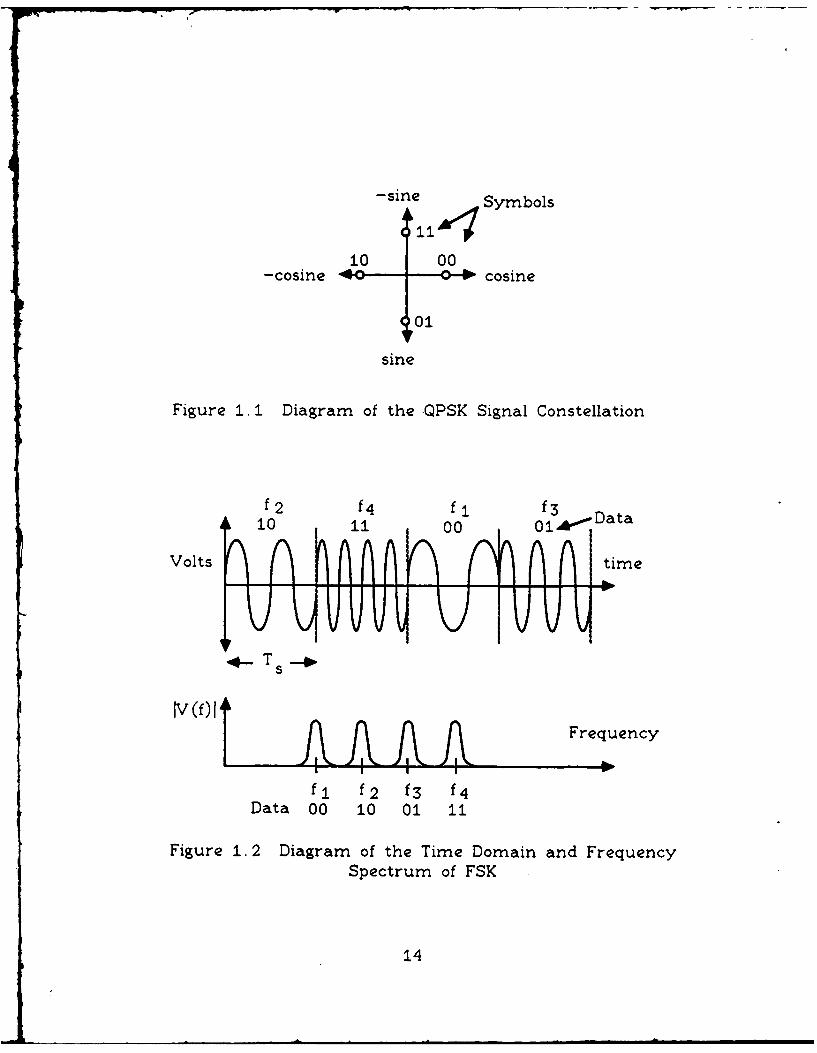
-sine Symbols
10 00-cosine cosine
01
sine
Figure 1. 1 Diagram of the QPSK Signal Constellation
f2 f4 f f3
0 00 0 1 aData
Volts t ime
Ts
Iv(f)11 Frequency
fl f2 f3 f 4Data 00 10 01 11
Figure 1. 2 Diagram of the Time Domain and FrequencySpectrum of FSK
14

-sine
k011 001 Symbols
010 0 0110 11 000-cosine cosine110
100 101
sine
Figure 1. 3 Diagram of the Signal Constellationof 8-PSK
15

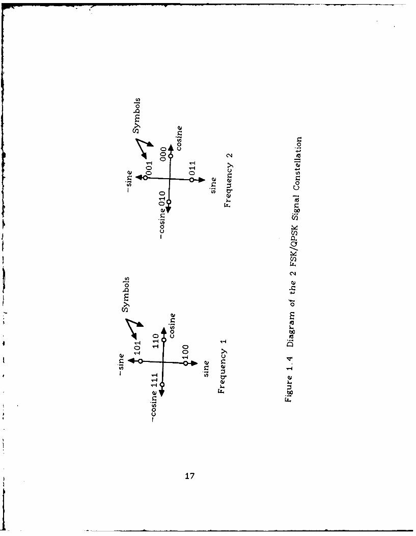
1. 2 FSK/QPSK
The modulation of the carrier waveform identifies the
communication method as PSK or FSK. The methods of
interest here are FSK and QPISK used together to create a
composite modulation form. The system considered in this
research uses two frequencies of the carrier with each
having four possible phases as shown in Figure 1. 4. This is
called 2 FSK/QPSK in this report.
2. Transmitter
The transmitter design of the 2 FSK/QPSK system is
a multiplexer as shown in Figure 1.5. The inputs to the
multiplexer are eight different carriers; each is selected by a
particular group of three bits of data. The selected carrier
is then transmitted.
3. Channel
An ideal channel would carry the message to the
receiver without errors. In practice, noise from the
environment is added to the signal. This noise creates
errors. A practical channel is modeled by adding Gaussian
noise to the signal as shown in Figure 1. 6. To simulate the
action of an intermediate frequency (IF) amplifier in a
typical superheterodyne receiver, the noise is bandpass
filtered and amplified before addition with the signal.
16
0
Cl)N
0 0
0-
0
0
0 E,~
0 QU
Qw
0
E1

Data Select
331coso t -0-cosoo t --- P
sinwo t --- o Output-sinwo t-10, MUx lo
cosw2 2t -400.
-coswo2t -Isinwo2t --- 10-sinw 2 t
Sil 2
Figure 1. 5 Design of the 2 FSK/QPSK Transmitter
s(t) from InputTransmitter nputo
X Receivern(t) s(t) + n(t)
Amplifier
Noise BandpassGenerator Filter
Figure I. 6 Design of the Channel Model
18

4. Receiver
Recovery of the bits of the 2 FSK/QPSK system is
accomplished using a coherent receiver shown in Figure 1. 7.
There are three parts to the receiver: the demodulator,
the integrate and dump circuit and the decoder.
Demodulation occurs in four separate mixers having different
local oscillators. Integration of the mixer output over the
symbol period produces voltages which are summed in three
channels of the decoder. The decoder uses a decision circuit
in each channel to recover the bits directly. The entire
receiver requires mixers, integrators, sample and dump
pulses, summers, sample and hold circuits and
comparators.
C. PLAN OF THE REPORT
This report presents a description of the research, the
experimental system, test results, analysis, experimental
performance and the conclusions.
The system design and description of the experimental
hardware are considered in three parts; the transmitter,
channel and receiver. Chapter II contains a description of
system operation. Subsystems and bit error detection
circuits are detailed in Chapter II1, and test results are
documented.
19

4-)
4, 4-'
0'
Q~
rw H 0 0
o cW
0
4-P4
44I
0
20

In Chapter IV, the performance of the experimental
system is compared with theory. The performance of the
experimental system is compared with the theoretical
performance of an 8-PSK system. Conclusions are drawn
from these comparisons. Appendix A contains circuit
schematics. Appendix B is a noise analysis of the 2
FSK/QPSK system.
21
II. DESCRIPTION OF RESEARCH
This chapter presents the theory of operation of the 2
FSK/QPSK system.
A. OBJECTIVE
This research measures and compares the performance
of the 2 FSK/QPSK system by designing, building and testing
a system. Performance is measured as probability of bit
error versus receiver input signal to noise ratio. This same
performance measure is determined analytically. These
results are compared with the theoretical performance of an
8-PSK system.
B. SYSTEM DESIGN AND THEORY OF OPERATION
The experimental system consists of the transmitter,
channel, receiver and bit error detection subsystems. These
are discussed in this section.
1. Transmitter
An analog carrier is modulated by pseudo random
data. Both the carrier and the random data are generated
in the transmitter subsystem shown in Figure 2.1. Three
data bits are transmitted as a symbol. Therefore, there
are 2 -3 8 symbols and, hence, 8 carrier states. These
22

u 3
II+ r.
32
+ 0 C4
3S
00M0+S
23

eight states are generated continuously in parallel. A
multiplexer (analog switch) is used to implement the
selection (transmission) of the carrier state corresponding to
the symbol sent.
The pseudo random data is produced by a feedback
shift register (FSR). The FSR has eight stages. Therefore,
the output binary sequence repeats after 28- 1 = 255
symbols. The clock rate is the symbol rate of transmission.
Three outputs of the possible eight from the FSR define the
symbol. These three outputs are applied to the control lines
of the multiplexer.
Two oscillators produce a square wave of frequency
I/Ts Hz and a- sinusoid of frequency f, Hz where Ts is the
duration of the symbol and f1 is one carrier frequency.
The square wave is the symbol clock. These two signals are
mixed to generate another carrier of frequency f 2 = fl +
l/Ts Hz. Then four phases of each of these carriers are
created using digital techniques. The result is the eight
carrier states.
2. Channel
In a typical communication system, noise is added
to the signal prior to demodulation. In this experiment,
this noise effect is duplicated by using a Gaussian noise
generator and a summer. Broadband noise is filtered to
24

represent the action of an intermediate-frequency (IF)
amplifier in a superheterodyne receiver.
3. Receiver
The receiver shown in Figure 2.2 consists of mixers,
integrators, summers, and circuitry to recover the data
bits.
Four mixers are used to demodulate the signal
received from the channel. The coherent references
required for the mixers are taken directly from the
transmitter in this research. The output of each mixer is
integrated over the symbol interval and then summed with
like voltages from three other channels to recover one of the
bits of the symbol. Summing four voltages permits use of a
zero threshold for bit recovery. The output of each
summer produces a positive or negative voltage,
representing a binary one and a binary zero respectively.
The bit is recovered directly using a comparator. This
circuitry is repeated with appropriate inputs to the summer
to directly recover the remaining two bits of the symbol.
Errors in data recovery are determined by
comparing on a bit by bit basis each of the transmitted
symbol components with the appropriate outputs of the
three comparators. Counters record the errors and the
total number of bits sent. The bit error ratio (BER) formed
from these counts is the probability of bit error.
25
o0
+ +
b)
0.0
00
26

IC. PERFORMANCE RESULTS
The analysis in Appendix B shows the 2 FSK/QPSKsystem to require about 5 db less signal power than 8-PSK
for the same bit error ratio. Experimental results differ
from theory by about 2 db.
r
27

III. EXPERIMENTAL SYSTEM AND RESULTS
The experimental system was built, using standard
linear and TTL integrated circuits, on "bread boards" and
"interfaced with various test equipment. The system consists
of the transmitter, channel, receiver and bit error detection
subsystems. This chapter discusses the design and operation
of each subsystem.
A. TRANSMITTER
The transmitter consists of the data generator and the
modulator as shown in Figure 2. 1.
1. Data Generator
In a 2 FSK/QPSK system, symbols are sent. Each
symbol represents one of eight different combinations of
three simultaneous data bits. To accurately test the
system, it is desirable to have the symbols occur in a
random manner. Therefore, it is necessary to generate a
data stream of random bits at a rate of rb/3 bits per second
and convert them to symbols. This is accomplished using a
feedback shift register (FSR) as shown in Figure 3.1. The
FSR is clocked externally by a square wave oscillator having
a frequency of 4 kHz = 2rb.
28

41
0
0
E
0 C
29

The feedback shift register produces a pseudo-
random data stream. An all zero state in the data stream
is not allowed because of the use of exclusive-or (XOR)
gates in the FSR. Should a FSR erroneously register all
zeroes, the FSR must be reset so that the psuedo random
sequence can continue. To reset the FSR, an "all zeroes
detector" circuit is implemented.
Three bits select any one of eight analog carriers at
the system bit rate (rb/3). This is accomplished by using
an analog switch (multiplexer).
2. Modulator
Digital data is used to modulate analog carriers in an
M-ary bandpass signaling scheme. In this research, the
analog carrier consists of one of two sinusoids of differing
frequencies, each having four possible phases. The method
by which these two sinusoids and their phases are generated
is described in this section.
a. Sinusoid of Frequency fi Hz
The sinusoid of frequency fj Hz is generated by
hard limiting and filtering a sinusoid of twice the frequency,
2fl Hz. A double frequency is chosen to provide sine and
cosine terms as discussed in the description of the phase
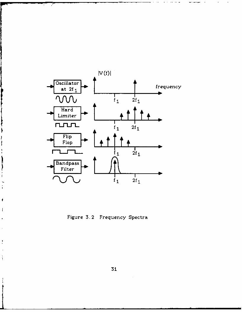
shifter. Figure 3. 2 illustrates the generation of a sinusoid of
frequency f, Hz.
30
OscillatorIVfItr ue cat 2f 1 frequency
(\ f\# 2fjHard
I "
ulj-L f. 2f 1
Flip
r jfl 2f "
Filter •
fl 2fl
Figure 3. 2 Frequency Spectra
31

In Figure 3.2, an oscillator at frequency 2fj Hz
creates a sinusoid which is applied to a hard limiter
producing a square wave of frequency 2fj. The square
wave frequency is divided by two by an edge-triggered flip
flop. The resulting square wave of frequency fj Hz is
bandpass filtered to produce the desired sinusoid of
frequency fj Hz, which is referred to as vi throughout the
remainder of this paper. Generating v1 provides only one of
the carriers necessary for the 2 FSK/QPSK system. The
other is provided by generation of a sinusoid of frequency f2
Hz.
b. Sinusoid of Frequency f 2 Hz
The process of producing v 2 , a sinusoid of
frequency f2 Hz, is more involved than the process of
producing vj. The sinusoid v 2 is generated by mixing,
filtering, hard limiting, phase shifting, and again filtering
two analog waveforms. Figure 3.3 illustrates this process.
Two analog waveforms are multiplied using an
analog voltage multiplier (AVM). The waveforms shown in
Figure 3.4, a sinusoid and a square wave, are generated by
two oscillators set at frequencies 2f 1 Hz and 2 rb/ 3 Hz
respectively. The product signal, also shown in Figure 3.4,
is bandpass filtered at a center frequency of 2fl- 2 rb/ 3 Hz.
Filtering recovers a sinusoid at frequency 2fl-2rb/3 = 2f 2
Hz.
32

* v(f)I
at 2f 1 f
2Ab/3 2f1
/I f
2r 2f1
~2rJ3+2f,~f + f
Narrow -A 2f -Bandpass Tfl. f
Filter
f'VWlfAAft 2f- 2r b/3=2f 2
Limiter t it4IL iIIFLLFL A 2f
Flip__Flop t _ _ _ _ _ _
Iadps f i-rb/3=f 2
Figure 3. 3 Frequency Spectra
33

ScaleVertical: 5 V/divHoriz: 0. 1 msec/div
Input Sinusoid, 2fl Hz
ScaleVertical: 5 V/divHoriz: 0.1 msec/div
Input Square Wave, 2 rb /3 Hz
Scale
Vertical: 5 V/divHoriz: 0.1 msec/div
Output of the AVM
Figure 3.4 Waveforms of the Transmitter AVM
34

The remaining process is similar to that found in
the generation of vI. Hard limiting produces a square wave
of frequency 2f 2 Hz. The square wave frequency is divided
by two using an edge-triggered flip flop. The resulting
square wave, of frequency f 2 Hz, is bandpass filtered to
produce the desired sinusoid v 2 of frequency -fl-rb/3 = f2
Hz. Four different phases of each of these two sinusoids are
then created using a phase shifter.
Observe that f 2 - fI = rb/3 = symbol rate =
I/Ts. This condition guarantees that v, and v 2 are
orthogonal on any symbol interval of Ts seconds. That is,Ts Ts
fvl(t)v2 (t) dt -- f cos2T (f 1 -f 2 )t at0 0
which is the area of one cycle of a sinusoid. This area is
always zero, independent of the "phase" of that cycle on the
interval.
c. Phase Shifter
The 2 FSK/QPSK system requires the four phases
of vj and v 2 to be generated and available for modulation.
Phase shifting v, and v 2 is accomplished through the use of
a hard limiter, a bipolar to unipolar converter, an inverter,
flip flops and bandpass filters. The process of shifting the
phase of v1 and v 2 is illlustrated in Figure 3. 5.
Phase shifting is performed by converting the analog
signal to a digital form, phase shifting the digital signal, and
35

4-0 40
4JU
4-J
4.4'
.0
014.'
*~0U)U
0.I'>
LU
364.

converting the digital signal back to an analog signal. A
sinusoid, at a frequency of either 2f, Hz or 2f 2 Hz is hard
limited. A sinusoid of twice the desired frequency is used
because the flip flops divide by two to produce a phase
shift. In this case, hard limiting is analog-to-digital
conversion.
The square wave is converted to digital form for TTL
compatibility. The digital square wave is inverted causing a
180 degree phase shift from the original digital square wave.
In turn, the original and inverted digital waveforms are fed
into leading-edge-triggered flip flops, causing a 90 degree
phase difference. A 90 degree phase shift occurs because
the flip flops act as divide-by-two circuits, thereby halving
the frequencies and the 180 degree phase shift.
The phase shifted digital square waves are bandpass
filtered, representing a conversion back to analog. The
sinusoids produced represent the sine and cosine signals at
frequency f, Hz or f2 Hz. The other signals, -sine and
-cosine, are produced using analog inverters.
The end result is that eight carriers, represented by
eight unique states of phase and frequency, are available for
transmission.
3. Multiplexer
Eight carriers are fed into a 3 x 8 multiplexer so
that the data is transmitted by selecting one of the carriers
37

with the psuedo random data symbols. The bit assignment
is shown in Table 3.1. An analog multiplexer represents a
switch whose output is selected by the symbol appearing at
the data selection inputs. Carriers are modulated in this
manner at the symbol rate = rb/3 symbols per second.
B. CHANNEL
The channel is depicted in Figure 3.6. A Gaussian noise
generator is used to provide a method of judging the
performance of the system in the presence of random noise.
The noise is bandlimited by a bandpass filter, amplified and
summed with the signal. After filtering and summing, the
noise plus signal voltage is applied to the demodulator.
C. RECEIVER
Analog signals are received via the channel for
demodulation and decoding so that bits may be recovered.
The entire process requires mixers, integrators, sample and
dump pulses, summers, sample and hold circuits and
comparators. These are all components of three
subsystems: the demodulator, the integrate and dump
circuitry, and the bit detection system. A description of
these three subsystems follows.
1. Demodulator
Demodulation occurs when the analog signals are
received and simultaneously mixed with four different local
38
TABLE 3. 1 BIT ASSIGNMENT FOR MULTIPLEXING
Code Word
Left Bit Middle Bit Right Bit Code Assignment
0 0 0 -cosw 2 t
0 0 1 +sinwot0 1 0 -cosolt
0 1 1 ++sinf2 t
1 0 0 -sincw 2 t1 0 1 +cosojlt1 1 0 -sinwlt1 1 1 +cOswo2 t
39

s(t) from InputTransmitter, to
X Receivern(t) s(t) + n(t)
AmplifierNoise ..1Bandpass ,,Geneato Filter Vi/ -
Genertor Bw = 2kHzl
Figure 3. 6 Block Diagram of the Channel Model
40

oscillators (LO's). This demodulation is achieved through
the use of AVM's as mixers and the sinusoids cosw 1 t,
sinwjt, cosw 2 t, and sinw 2 t as LO's as shown in Figure 2.2.
The output of each mixer is low pass filtered and integrated
over the symbol interval of Ts sec.
2. Integrate and Dump Circuit
Integration of the mixer outputs over the symbol
interval produces any one of three voltage levels, depending
upon which analog symbol is sent. Regardless of which
analog symbol is sent, the output of one of the four
integrate and dump circuits at the end of one symbol
interval is always a positive or negative voltage. The
remaining three integrate and dump outputs are zero volts.
The outputs of the mixer and integrate and dump are
described on a case by case basis.
There are eight different possible combinations
produced at the output of each of the mixers. In turn,
each of these produces a particular output in the integration
process. We examine all cases in which the received signal
is mixed with the LO of sinwit.
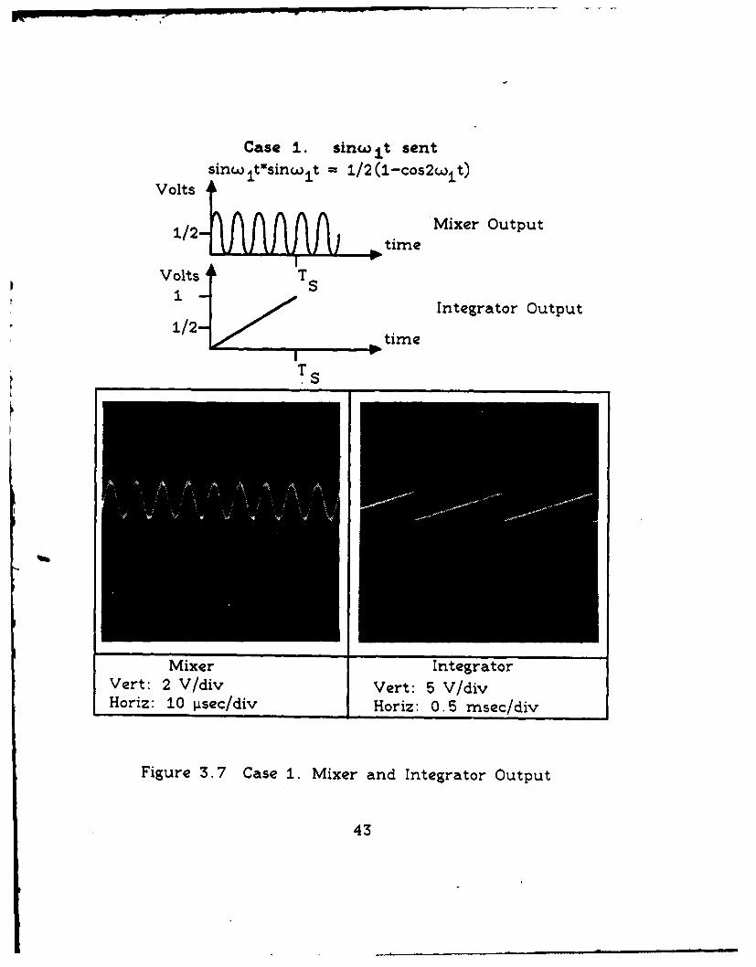
Case 1. Assume that sinwot is received. TheI
analytical expression for the output of the mixer is
sinwl (t)sinwl (t) = 7(1-cos2wlt) . (3.1)
41
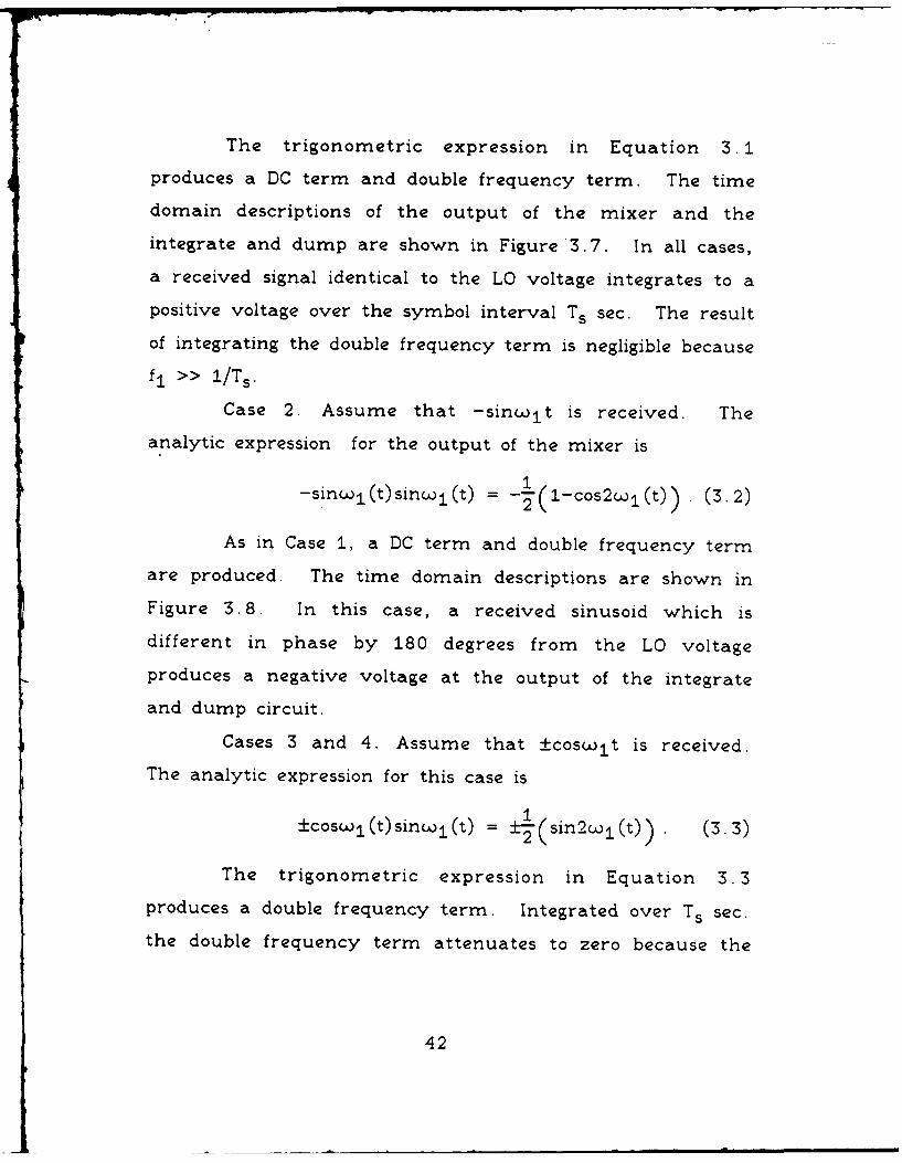
The trigonometric expression in Equation 3. 1produces a DC term and double frequency term. The time
domain descriptions of the output of the mixer and the
integrate and dump are shown in Figure 3.7. In all cases,
a received signal identical to the LO voltage integrates to a
positive voltage over the symbol interval Ts sec. The result
of integrating the double frequency term is negligible because
f» >> 1/Ts.
Case 2. Assume that -sincolt is received. The
analytic expression for the output of the mixer is
-sinwl(t)sinwl(t) = --L(1-cos2wj(t)) . (3.2)
As in Case 1, a DC term and double frequency termare produced. The time domain descriptions are shown in
Figure 3. 8. In this case, a received sinusoid which is
different in phase by 180 degrees from the LO voltage
produces a negative voltage at the output of the integrate
and dump circuit.
Cases 3 and 4. Assume that ±coswlt is received.
The analytic expression for this case is
±coswl(t)sinwl(t) = 2 (sin2w,(t)) . (3.3)
The trigonometric expression in Equation 3.3produces a double frequency term. Integrated over Ts sec.
the double frequency term attenuates to zero because the
42
Case 1. sinw 1 t sentsincwlt*sin:,1 t = 1/2(1-cos2w,1 t)
Volts
Mixer Output1 ____________time
Volts T•S
Integrator Output1 / 2 0 000_ tim e
S~TS~S
Mixer IntegratorVert: 2 V/div Vert: 5 V/divHoriz: 10 g.sec/div Horiz: 0.5 msec/div
Figure 3.7 Case 1. Mixer and Integrator Output
43

Case 2. -sinwjt sent
-sinwjlt~sinw:$t = -I/2(1-cos2w:1 t)
Volts I__ __time
-1/2 i fv j\JvJ Mixer Output
SVolts time
Volt Integrator Output
Mixer IntegratorVert: 2 V/div Vert: 5 V/divHoriz: 10 psec/div Horiz: 0.5 msec/div
Figure 3.8 Case 2. Mixer and Integrator Output
44

Case 3,4. ±cosw lt sentsinw t*cosw 1t = 1/2 (sin2w 1t)
/ Mixer Output
TSS Integrator Output
1/2 time
T S
Mixer IntegratorVert: 2 V/div Vert: 5 V/divHoriz: 10 psec/div Horiz: 0.5 msec/div
Figure 3.9 Case 3 and 4. Mixer and Integrator Output
46

Case 5, 6, 7,8. ±sinw 2 t or ±cosw 2 t sent
sinwilt~sinw 2 t = i/2(cos(.wl-w 2 )t-cos(wi±+w,2)t)
MixerA
IntegratorT
1.
time 1/2time
Mixer
Integrator
ScaleVertical: I V/div Horiz: 0.5 msec/div
Figure 3.10 Case 5,6,7 and 8.Mixer and
Integrator Output
47

Scale
Vertical: 2 V/divHoriz: I msec/div
Integrate and Dump Output (No Noise)
ScaleVertical: 2 V/divHoriz: 1 msec/divNoise = 6 dB
Integrate and Dump Output(With Noise)
Figure 3.11 Integrate and Dump OutputsWith and Without Noise Added
49
L .. m mm m m

+5V+5V • Multiplexer _
Dump Pulse l (Switch) "Dý
r-(t) T 1s
Op AmJ r (t) dt+ 10
Figure 3. 12 Diagram of the Integrator
50
no
maximum value (no noise case). This insures optimum bit
detection. The sample and dump pulse duration is small
compared to the symbol interval (integration period). After
the sample pulse, the dump pulse is used to begin the
integration process again for one symbol interval. The
dump pulse is made dependent upon the trailing edge of the
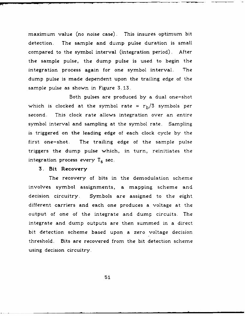
sample pulse as shown in Figure 3. 13.
Both pulses are produced by a dual one-shot
which is clocked at the symbol rate = rb/3 symbols per
second. This clock rate allows integration over an entire
symbol interval and sampling at the symbol rate. Sampling
is triggered on the leading edge of each clock cycle by the
first one-shot. The trailing edge of the sample pulse
triggers the dump pulse which, in turn, reinitiates the
integration process every Ts sec.
3. Bit Recovery
The recovery of bits in the demodulation scheme
involves symbol assignments, a mapping scheme and
decision circuitry. Symbols are assigned to the eight
different carriers and each one produces a voltage at the
output of one of the integrate and dump circuits. The
integrate and dump outputs are then summed in a direct
bit detection scheme based upon a zero voltage decision
threshold. Bits are recovered from the bit detection scheme
using decision circuitry.
51
clock timing time
time
sample pulsetime
dump pulse-- • tim e
clock timing
integrator
sample pulse
dump pulse
ScaleHoriz: 500 psec/div Vert: 5. 0 V/div
Figure 3.13 Timing Diagram of Sample andDump Pulses
52

The integrate and dump output voltage combinations
shown in Table 3. 2 are the result of symbol assignments
made in the first two columns where C1 ,Si,C 2 and S2
represent the channel integrate and dump circuit outputs
shown in Figure 2.2. In Table 3.2, symbols 0, + and - all
represent maximum voltage levels at the time the
integrator is dumped. For any given symbol interval a
positive or negative voltage is at the output of one of the
integrate and dumps. The remaining three integrate and
dump output voltages are zero. The three possible voltages
at the output of the integrate and dump circuits provide a
voltage ambiguity when recovering data bits of ones and
zeros. This ambiguity is eliminated by a logical analysis of
the integrate and dump outputs C1 ,S 1 ,C2 and S 2 . The last
three columns of Table 3.2, physically realized by three
four-input summers, constitutes a mapping scheme derived
from an analysis of the ambiguities. The summers combine
the integrate and dump outputs to produce positive or
negative voltages on which decisions are made and bits are
detected. Output of the summers with and without the
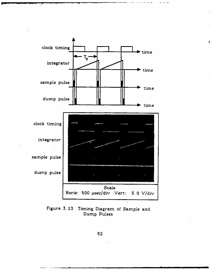
influence of noise are illustrated in Figure 3.14.
The three summer outputs are applied to the
decision circuitry as shown in Figure 3. .5. The decision
subsystem consists of sample and hold and comparator
circuits. The positive or negative voltage produced by the
53

TABLE 3.2 INTEGRATOR OUTPUT TO SUMMER MAPPING
Symbol Assignment Integrator Voltages Summer Voltages
C1 -S 1 C2 -C 1 CI+S1
+ + +
Symbols Signals C1 S1 C2 S2 C2 -S 2 $2-SI C2 + S2
Left Middle Rig•:t
Bit Bit Bit
000 -cosw 2 t 0 0 - 0 - - -
001 +sinwilt 0 + 0 0 - - +
010 -coso(lt - 0 0 0 - + -
011 +sinw 2 t 0 0 0 + - + +100 -sinw 2 t 0 0 0 - + - -
101 +cosojlt + 0 0 0 + - +
110 -sinwlt 0 - 0 0 + + -
ill +CosoA2 t 0 0 + 0 + + +
54
ScaleVertical: 2 V/divHoriz: 1 msec/div
Summer Output Without Noise
ScaleVertical: 2 V/divHoriz: 1 msec/divNoise = 6 dB
Summer Output With Noise
Figure 3.14 Output of a Four-Input Summer, Withand Without Noise Added
55

+C 1
k ummer Comparator
Left Bit
+CSample2and Hold I___
-S2
-Cl-Si 4
°S ummerComparator Middle Bit
Sample+S2 and Hold
+C 2
+Ci+ S j + S m m r 1%
-
\ ummer Comparator Right Bit
Sample+C, 2 and Hold
+S 2
Figure 3.15 Block Diagram of Decoding Circuitry
56

four-input summer is held at a constant voltage by a
sample and hold circuit for one symbol interval of Ts sec.
Based upon a zero threshold, the comparator decides a
positive voltage is a one and a negative voltage is a zero.
From the output of the comparator the bits are recovered
directly.
D. BIT ERROR DETECTION CIRCUIT
Performance of a system is judged by the number of
errors made when random Gaussian noise is added. The
errors are detected by comparing the recovered data with a
delayed version of the transmitted data. A delay in the
transmitted data is necessary to compensate for delays
experienced in the receiver. From this comparison, the bit
error detection circuit counts the number of errors for each
bit channel and the number of symbols sent. Three bits
are sent simultaneously. Therefore the bit rate in each
channel is equal to the symbol rate so that the symbol
counter is also used as a bit counter. The ratio of errors to
symbols sent is the bit error ratio (BER) which is a
measure of system quality.
The bit error detection circuit for this system is shown
in Figure 3.16. The transmitted data is compared with the
recovered data on a bit by bit basis using an XOR gate. If
the data bits are the same, the XOR stays low. Before the
57

TransmittedData O
Sample -. AND [Pulse Error Counter]
Recovered ANDData -E-0.
Start/Stop Bit Counter+5V
System Clock
Figure 3. 16 Block Diagram of the Error Detection Circuit
58

data is compared, each data pulse is strobed using AND
gates. The strobe is identical in nature to the sample and
dump pulse described earlier. Data is strobed at the center
of each pulse to eliminate errors due to the edges (switching
times) of the pulse. If the bits differ, an error is counted.
The error detection circuit is stopped and started by an
external switch and another set of AND gates as shown in
Figure 3.16.
E. TEST RESULTS
Errors are counted for various levels of noise injected
into the channel. This variable noise level is used to change
the system signal-to-noise ratio (SNR). Communication
system performance is presented as a plot of probability of
error Pe = BER versus SNR. The resulting curve is
compared to that of a more conventional 3ystem. Here,
the 2 FSK/QPSK system is compared to an 8-PSK system.
An 8-PSK system is chosen because 8-PSK system
performance is known, it is similar to the 2 FSK/QPSK
system, and 8-PSK is popular.
1. SNR versus Pe
The experimental data taken for varying levels of
SNRP is shown in Table 3. 3. SNR. is measured using a true
RMS voltmeter. The signal power S and the signal plus
noise power (S+N) at the output of the channel summer are
59

TABLE 3.3 EXPERIMENTAL DATA
S/N M e PeLeft Middle Right Total
(dB) Bit Bit BitLB MB RB 1/3 (PeLB+PeMB+PeRB)
3 2.80X10- 2 2.09X10- 2 2.06x10- 2 2.32X10⁻²
4 1. 30x10- 2 9. 16x10- 3 9.56x10- 3 1. 06x10-2
5 6.08X10- 3 4.67x10- 3 4.82x10⁻³ 5.44x10⁻³
6 3.56X10O3 2.06X10- 3 2.46X10- 3 2.70X10⁻³
7 1. 20X10- 3 6. 07x10- 4 1. 01X10- 3 9. 39x10-4
8 6.47X10- 4 3.44X10- 4 4.03X1O- 4 4.65X10⁻⁴
9 2.72x10- 4 9.53X10- 5 1.48X10- 4 1.72x10⁻⁴
10 3.33X10⁻⁵ 1.11xio- 5 2.88x10- 5 2.44X10⁻⁵
11 1. OxiO-5 6.67x10- 7 7.33x10⁻⁶ 6. OOX1O-6
60
measured using a true RMS voltmeter. The noise power is
then determined by subtracting the signal power S fromS
S+N. The SNR = S or in db,
SNR (dB) = 10 log (S).
The probability of error Pe of the system is
calculated by first determining the probability of bit error in
each bit recovery channel for various values of SNR and
then averaging the three channel results.
Probability of bit error Pe for each channel is
calculated by dividing the total bit count by the error count
for that particular SNR.
error countPe = bit count
The counts are obtained from the error detection circuit.
The three bit recovery channels combine to produce Pe
where LB is the left bit, MB is the middle bit and RB is the
right bit.
Pe = 3'(PeLB+PeMB+PeRB)
This is calculated for a SNR from 3 to 11 db.
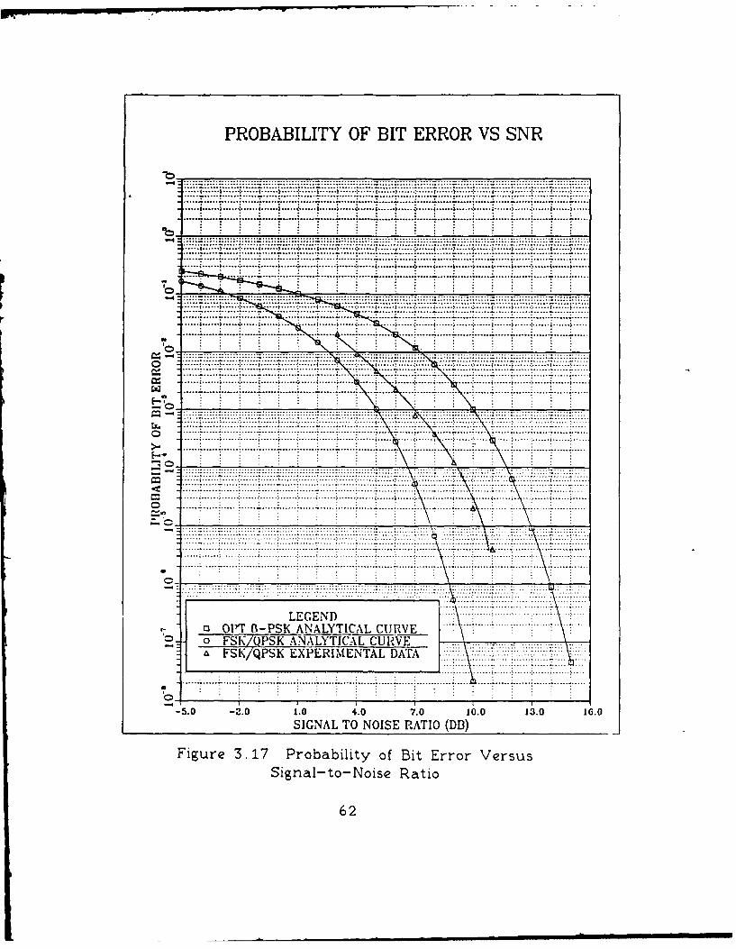
The data is plotted in terms of Pe versus SNR. Figure 3. 17
illustrates the characteristic waterfall curves for the 2
FSK/QPSK system and the 8-PSK case. The 8-PSK curve is
a basis for comparison.
61
PROBABILITY OF BIT ERROR VS SNR
..............
.0 .. .. .... . .. .. ..... . ... ... .. .. ..... .. .... .. z .. .. .. ..
0. .. .. ... .. . . .. . ..... . .. ... ...... .... ..... ... . .. ... .. .. ..
........ .. .. *,*,,-!a.... . ,- -ý.... I.... ....-...........o ..
.. ..... ...... .. .. ..... ...... ..... ......... ... ............... ... ..0. ..... ...... ...... ......... .... .. ......
.. .... .... ........ ....... ..0. ................. .. ......
O . ..... AALTICL.CRV- o FSKQPSK A. LYTI.L.C...
FS ..... EX.IM N A ... D ..............A.....
..... I . .. . . . . . . . . . . . . .. . . . . . . . . . . . . . . .- .... -2...0 ... 0 4.0.. . 0...... 10...... 0... 1....... 0.......... 1... 0
........ SIGNA.. L TO.. NO S RATI ... ...... D.........1......3 ....... ...
Fiue307 Poaiit fBtErrVruSi0lt- os Ratio..
6 2....... .N ............J......... . ......

2. Comparison
Figure 3. 17 shows a 5 db improvement of the
experimental system relative to the theoretical 8-PSK
system. The experimental system differs from the theory
of Appendix B by 1.5 db to 2.5 db.
3. Results
The theoretical noise performance of the 2 FSK/QPSK
system is derived in Appendix B and plotted in Figure 3.17.
The results for 8-PSK are also given in that figure [Ref. i].Finally, the measured performance, averaged over the three
bits of the symbol, is also plotted in Figure 3.17.
63

IV. CONCLUSIONS AND RECOMMENDATIONS
A. CONCLUSIONS
The analytic results of the 2 FSK/QPSK system shows a
5 dB power advantage relative to 8-PSK. This advantage is
caused by the use of a third parameter (dimension) in the
constellation diagrams. This parameter is frequency and it
allows a "separation" of the carrier states which cannot be
realized with 8-PSK. It is well known from decision theory
that increasing the distance between "signals" reduces
probability of error.
The experimental results differ from theory by 1.5 db to
2. 5 db over the range of SNR used. This discrepancy is
caused by differences in the four demodulation channels in
the operating receiver. Considerable time may be required
to adjust the circuitry until all four channels have nearly
identical performance. Such adjustment is required before
the experimental results will duplicate the theoretical
results.
B. RECOMMENDATIONS
It is recommended that extensions of this work include
adjusting the circuitry to obtain closer agreement between
measurement and theory. Further, work should proceed on
64

the design and implementation of circuitry to derive carrier
and bit synchronization from the received noisy signal.
65

APPENDIX A
CIRCUIT SCHEMATICS
This section contains schematic diagrams of the
subsystems and individual circuits of the 2 FSK/QPSK
system. Standard Linear and TTL integrated circuits are
used. Specifications for all integrated circuits can be found
in References 2, 3 or 4. Unless stated otherwise, resistor
values are in kf), capacitor values are in piF and op-amps
and comparators are powered by voltage supplies of +14 and
-14 volts. Most op-amp applications use LF356N high speed
op-amps because of the high slew rates required for
frequency operation in the 50 to 150 kHz range.
A. TRANSMITTER
The transmitter consists of the data generator,
modulator and phase shifter subsystems as shown in Figure
3.1. Hard limiters, bandpass filters, an AVM and several
frequency dividers are used. Two oscillators feed the
system to produce the modulated carriers and generate
data. One oscillator produces a sinusoid of frequency 2fl =
115.366 kHz. The other oscillator produces a square wave
of frequency 2 rb = 4.000 kHz.
66

Figure A. 1 shows the circuit schematic for the data
generator. The 74LS164 feedback shift register (FSR)
produces a psuedo random data stream [Ref. 2: p. 280],
Because XOR gates are used as feedback components, the all
zeroes state is disallowed. Combinational logic using NAND
gates detects the all zeroes state and reinitiates the FSR,
data stream. The FSR is clocked at a rate of rb/3 = 667
Hz. The clock is derived from the system oscillator
producing a square wave of frequency 2rb Hz and a divide-
by-six circuit.
The divide-by-six circuit is shown in Figure A. 2. The
bipolar square wave from the oscillator is converted to a
TTL compatible unipolar square wave in the MC1489
monolithic quad line receiver [Ref. 3:p. 5-120]. Division
by six is realized by the configuration of a single 7492
counter integrated circuit. This circuit is clocked by the
unipolar square wave of frequency 2rb Hz, thereby
producing a square wave of frequency rb/3 Hz.
A divide-by-three circuit is necessary in the transmitter
because one of thc inputs to the AVM which produces v 2 is
a square wave of frequency 2rb/3 Hz, one third of the
square wave oscillator frequency. The divide-by-three
circuit consisting of a dual JK edge-triggered flip flop is
shown in Figure A.3.
67

Input to Multiplexer
+5V+
1413 12 11 10 9 8V H G F E CLRCLK
74164 (FSR)
S1 S2 A B C D GND
1 2 3 4 5 6 7
+5V
11 137400 •1
2 6 67486
S7430 8
FSR Outputs
All Zeros Detector
Figure A. 1 Circuit Diagram of the Data Generator
68

+5V
14 13 12 11 10 9 8V ID CD OD IC CC OC
cc1489
IA CA CA IB CB OB GND1 2 3 4 5 6 7
From Oscillator I I
_ _ _ Output to FSPR
14 13 12 11 10 9 8CLK1NC Q1 Q2GND Q4 Q6
7492 (Divide-By-Six)
CLK2 NC NC NC V 0 01 2 3 4 5c CC eet 7s et
+5V
Figure A. 2 Diagram of the Divide-By-Six Circuit
69

Clock
3 5 Outputj 2 Q 2
12 1 1 2 2
CLK 74107 - CLK 74107+6V o- K 5 __K Q
4 1
Figure A. 3 Diagram of the Divide-By-Three Circuit
70

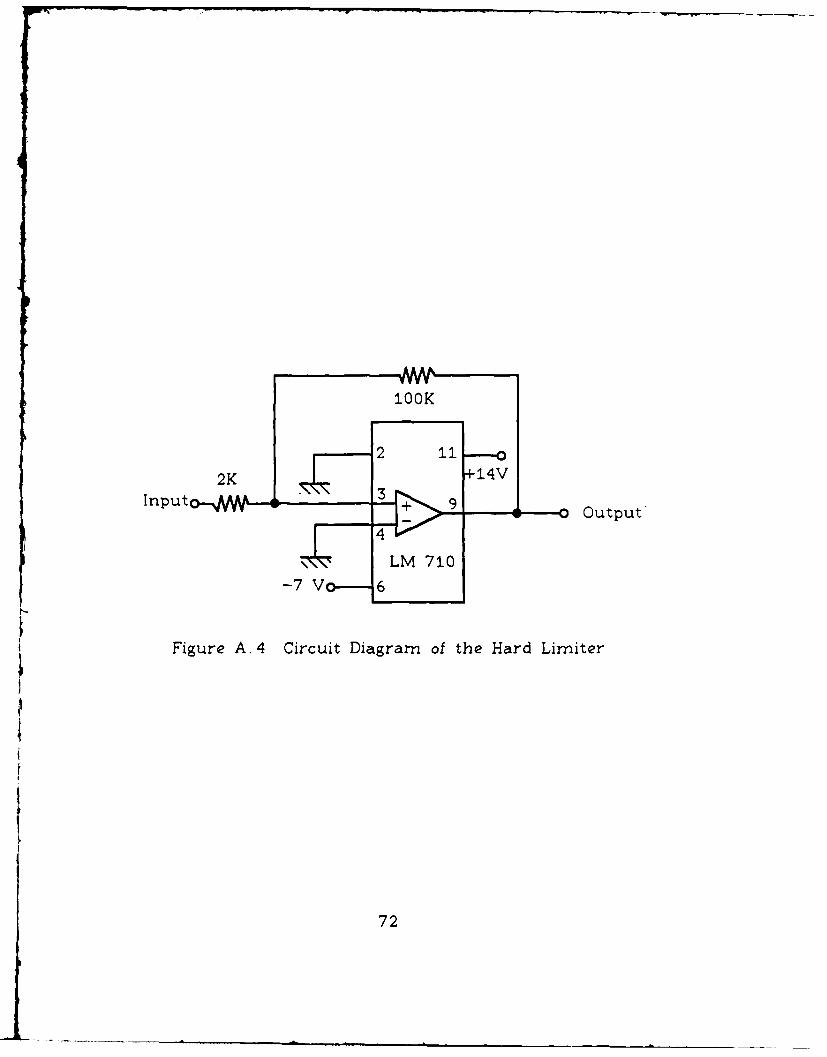
Figure A.4 is a schematic diagram of the hard limiter.
The hard limiter is an LM710 high speed voltage
comparator. It requires voltage biasing of +14 volts and -7
volts. This arrangement converts an analog sinusoid into a
digital square wave.
Two types of filters are shown in the transmitter block
diagram (Figure 2.1). A bandpass filter and a narrow
bandpass filter are both variations of the biquadratic
bandpass filter realization shown in Figure A.5. The
biquadratic bandpass filter design permits simplicity,
flexibility and accuracy in the design process. [Ref. 5]
The narrow bandpass filter design requires a 3 dB
bandwidth of 2 kHz and a center frequency of 114.031 kHz,
2fl - 2rb/3 Hz. To achieve this, the design consists of six
stages of the filter realization shown in Figure A. 5 where R
= 2700, C = 0.005 pF and R 5 = 27 k!Q. The frequency
response for the narrow bandpass filter is shown in FiguresS~A. 6 and A.7. Figure A. 8 shows the narrow bandpass filter
frequency response superimposed over the spectrum of the
output of the mixer to illustrate the filter effectiveness.
The bandpass filters in the phase shifter have a 3 dB
bandwidth of 34.2 kHz and a center frequency of 57.683 or
57.016 kHz (fl or f2 Hz). The filter decign consists of a
single stage of the circuit shown in Figure A. 5 where R
71
ALA
lOOK
F2
2K ,•3+14V
Input+ 9 G _ 9-0 Output
•-•LM 710
-7 V --- 6
Figure A. 4 Circuit Diagram of the Hard Limiter
72

i:1II "4J
'0,j ~,,
>:>
+ VI 4
[ .0
>0
V, V,
v-4+U
CN M LO
bO
73

ZE) IL
00
m-P JW E
V4 0
-74

I Eicm xo0
z C)
.11)t
U))
- to
It
zD
E 575

I NIDI
In - - - - -- - - -. a
-4
~~a- . 0
EnO
0)U z o
< N0 1 E
Z0 Li..
'4.0 ff m C
awz
m -i.
0 C
.0.l
0u
C76

1.8 kQ, R5 = 1.8 ki and C = 0.005 pF. The filter
response of this filter design is shown in Figures A. 9.
Figure A. 10 is the wiring diagram for the analog voltage
multiplier (AVM). The AVM is a monolithic laser trimmed
voltages multiplier. The schematic shown is the basic
multiplier connection [Ref. 4].
Figure A.11 is a circuit diagram of the phase shifter.
The LM710 hard limiter receives a sinusoid and converts it
to a bipolar square wave. The bipolar square wave is
converted to a TTL compatible unipolar square wave in the
MC1489 monolithic quad line receiver. An inverter phase
shifts the "phase" of a square wave by 180 degrees. In
turn, the original and inverted square waves are fed into
separate leading-edge-triggered flip flops, producing a 90
degree phase shift difference. The timing of the phase shift
is also shown in Figure A. 7.
The unity gain inverter which produces the remaining
carriers after bandpass filtering is shown in Figure A. 12.
The schematic of the modulator is shown in Figure
A.13. A 4051B single 8-channel analog multiplexer/
demultiplexer is used. Three binary control inputs select
one of the eight carriers to transmit data. Switching occurs
at the rate rb/3 Hz.
77

X Em
a. 0
U)
CD,
0*
LL.
I U)
co J 0rOuz - -wwI-u
78~

l | -n- -
n -
, , • . ..
XlX2 1 14 -+14V
X 2 12 --(xi)*(¥1)J•. AD534
Yl 6 10Y2 7 8 77-77ý o0 -14V
Figure A. 10 Circuit Diagram of the Analog Voltage Multiplier
79

+14V
14 13 12 11 10 9 8VA A MC 1489C
IN OUT GN2 3 4 5 6 7 _
Flip Flop 7410
,, ,•V +5V+5V +5
+14V 100K ? ? I? ? ?v114 13 12 11 10 9 8
Flip Flop 74107I
14 13 12 11 10 9 8 IJ M 1Q 1K 2Q 2QGNDV OUT 123 4 5 6•7
LM 71OCNGND IN IN +5
72. 2K 2. 2K
Input -7V
+5V +5V
2K Output to Filters
• +5V
Input 0
-5V
1Q Output +5V0
•_o o u• II [-- +5v2Q Output +5V
Figure A.11 Circuit Diagram and Timing of thePhase Shifter
80

20K
Inut 20K• I LF356 8 +4
2n 7 .--.o
36 6 0
* 4 Outputo 4 5
-14V
Figure A. 12 Circuit Diagram of the Analog Inverter
81

Digital Selection
tAnalog Inputs
DD 1 0 3 A B
CD4051B (MUX)
1 2 4 5 6N 7EE 8 ss
Output Channel
Figure A.13 Circuit Diagram of the Multiplexer
82

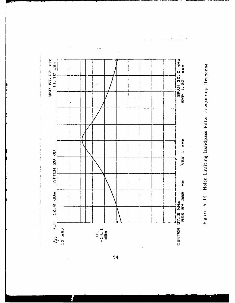
B. CHANNEL
The channel consists of a summer, bandpass filter and
amplifier. The amplifier is similar to the analog inverter
shown in Figure A.8 with the exception of the feedback
resistor which is varied to produce a larger or smaller gain.
The bandpass filter is two stages of the biquadratic bandpass
filter shown in Figure A.5. where R. = 277 0, R5 = 7.9 kQ
and C = 0. 01 pF. The 3 dB bandwidth of this filter is 2
kHz. The frequency response of this filter is shown in
Figure A 14.
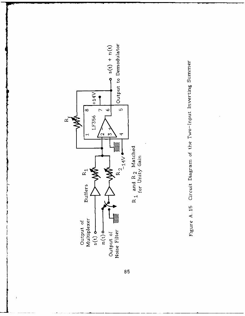
A two-input summer shown in Figure A. 15 injects
Gaussian noise into the system. A switch enables and
disables the noise source. Two LF356 op-amps configured as
voltage followers are buffers for impedance matching. R1 ,
R2 and Rf are precision resistors matched for unity gain.
C. RECEIVER
The receiver consists of mixers, integrate and dump
circuits, sample and dump pulse generators, a decoding
subsystem and an error detection subsystem.
The AVM shown in Figure A.16 mixes the received
signal with a local oscillator. This configuration is identical
to the AVM shown in Figure A.10 except that Figure A.16
is followed by a passive lowpass filter. The lowpass filter
83
N~ Gr
in 4
u) a
LzL.
j~b2
t. w
Ul
w3
4~0
00.4--) (
ob
000
U 0
>S
'4-. 'E-
U, ~ 0
85u

From Local Oscillator
0- 1 11 X*Y -- 1 V Output2 12_] -W _ o•: AD534 10K -7 o. 01pF
From Channel 11[ y 6 1 Lowpass Filter
Figure A. 16 Circuit Diagram of the Analog
Voltage Multiplier and the Lowpass Filter
86

eliminates high frequency terms. Filter characteristics are
R = 10 kn and C = 1.0 PF.
A schematic of the integrate and dump circuitry is
illustrated in Figure A.17. A multiplexer and dump pulse
represent an analog switch which resets the integrator after
each symbol interval. The inverse of the integrator output
is made available through the use of an analog inverter.
Both polarities are necessary in the decoding scheme,
Figure A.18 shows the circuit diagram of the sample
and dump pulse generator. Both pulses are produced by a
74221 dual one-shot. The dump pulse is made dependent
upon the sample pulse so that sampling at a maximum
voltage occurs prior to dumping the integrator. The sample
pulse is triggered by the leading edge of the clock at a
frequency of rb/3 Hz, In turn, the trailing edge of the
sample pulse triggers the dump pulse. Pulse width of the
sample and dump pulses is much shorter than the clock
pulse width and can be adjusted with the 20 kQ variable
resistors.
As shown in Figure A.19, the decoding circuitry consists
of a four-input summer, a sample and hold circuit and a
comparator. The four-input summer is an extended design
of the summer in the channel circuitry. Precision resistors
R1 , R 2 , R3 and P,4 are identical. Rf is adjusted to produce
unity gain. The LF398N sample and hold circuit is clocked
87

Dump Pulse+5V +5V
(F161614 13 121110 9V 2 1 0 3 A B C
DD
MC 14051 B
4 6 OUT/1N7 5 1 V VNN EE SS
12 3 4 56 78_
Open Circuit I
Dump Pulse
0. 01pFI[ 50k
+14V4A
PO•0 LF 35 -7Output= 10lk LF
-14V
Integrator 14VI nverter
Figure A. 17 Circuit Diagram of the Integrate and Dump
88

+5V __ _ _ _ _
Sample
+v20K 0.1F+15V Pulse+5V5
16 15 14 13 12 11 10 9V 1R/C IC IQ 2Q 2CLR2B 2A
Cc ext ext
74221 Dual 1 Shot
1A1B1CLR1Q 2Q 2C 2R/C GNE1 2 3 4 5 6 ex 7 8
Clock +5V 20K
Dump 0. luFPulse , +5V
Clock Timing A time
"time
Sample Pulse
time
Dum p Pulse tim
Figure A, 18 Circuit Diagram of the Sample/Dump
Pulse Generator
89
0
4-J-
> 0
>>
] r-
0T)-
00
- U•
> >000
v-) c4> 0
0u~ bO
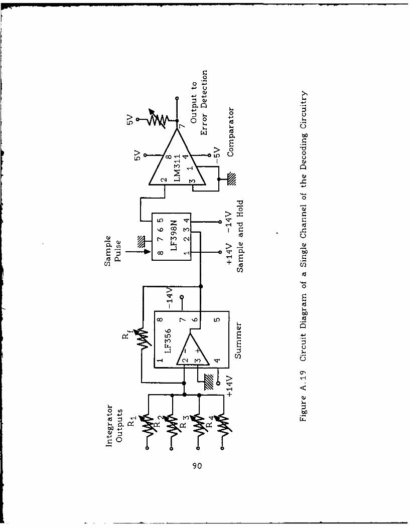
90
by the sample pulse shown in Figure A. 18 at a rate of rb/3
Hz. The LM311 voltage comparator is the decision circuit of
the system. Based upon a zero voltage threshold, the
comparator decides a negative voltage is a binary zero and
a positive voltage is a binary one. The output voltage of
the comparator is +5 Volts or 0 Volts.
The bit error detection circuit is shown in Figure A. 20.
The transmitted data is compared with the recovered data
on a bit by bit basis using an XOR gate. If the data bits
are the same, the XOP. stays low. Both data pulses are
strobed using AND gates. The strobe is produced by a dual
one-shot which uses 20 k!Q variable resistors to position the
data strobe at the center of each data pulse where the first
pulse determines the time delay of the sample pulse. This
eliminates errors due to the edges (switching times) of the
pulse. If the bits differ, an error is counted. The error
detection circuit is stopped and started by an external
switch and another set of AND gates.
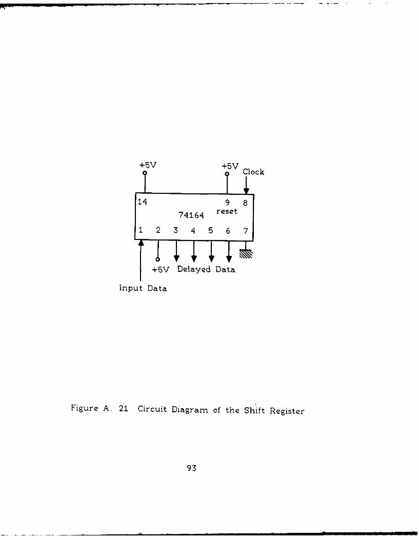
Figure A. 21 is a shift register circuit which delays the
transmitted data before it is compared with the received
data in the error detection circuit. The transmitted data
must be delayed to compensate for delays in the receiver.
91

+5V
Pulse Width Shot
20K k (.1F+14V
+5V 0.lp
16 14 13 12 11 10 9
V 1R/C 1C 1Q 2Q2CLR2B 2ACc ext ext
74221 Dual 1 Shot
IAIBICLRIQ 2Q 2C 2R/C _GNE1 23 4 5 6 ext7 8
20K+5V
Clock 0. lpF
Sample Pulse+5V
Transmitted Data
Recovered Data -0'[_. .• 7408
Start/Stop I• Bit Counter
+5V
System Clock
Figure A. 20 Circuit Diagram of the Error DetectionSubsystem
92
I
+5V 5V Clock
14 9 874164 reset
2 3 4 5 6 7
+5V Delayed Data
Input Data
Figure A. 21 Circuit Diagram of the Shift Register
93

APPENDIX B
DERIVATION OF THE 2 FSK/QPSK PROBABILITY OF BITERROR EQUATION
The receiver decision process is based on the voltage
value of vs(t) shown in Figure B. 1. Samples are taken at
the end of each symbol interval of duration Ts seconds. If
vs(Ts) is greater than zero at the sample time, then a
binary one is decided. If vs(Ts) is less than zero, then a
binary zero is decided. Therefore, decisions are based on
summer output voltage levels at the end of each symbol
interval.
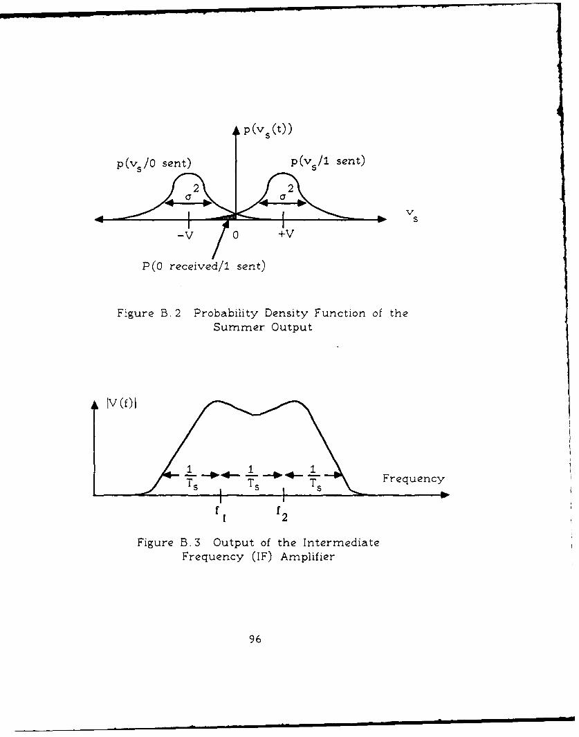
To determine that probability of bit error, the
probability density functions (pdf's) of vs(Ts) given a one
sent and given a zero sent are required. . Figure B. 2 is an
example of these two pdf's having mean values of +V volts
and -V volts and variance of a 2 watts.
The receiver model of a typical receiver channel (one of
four used) is shown in Figure B. 1. The following analysis
uses the noise model of Rice [Ref. 6]. Assume
vi(t) = Acoswit + n(t) (B. 1)
and vr(t) = cosj 1 t , (B. 2)
94

4-o
0
4-' -
(1~ u
t..
095
p (v (W))
p (v s/0 sent) p (vs /1 sent)
P(0 received/i sent)
Figure B. 2 Probability Density Function of theSummer Output
IV W)I
Ts Frequency
f fI12
Figure B. 3 Output of the IntermediateFrequency (IF) Amplifier
96
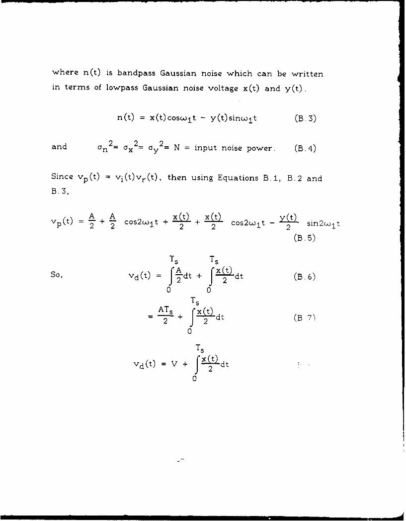
where n(t) is bandpass Gaussian noise which can be written
in terms of lowpass Gaussian noise voltage x(t) and y(t).
n(t) = x(t)coswlt - y(t)sinwlt (B. 3)
and Onx 2x= ay2= N = input noise power. (B. 4)
Since Vp(t) = vi(t)Vr(t), then using Equations B.1, B.2 and
B. 3,
A A + x(t) + x(t) s2t sinVp (t) + cs2it +2 2 2
(B.5)
Ts Ts
So, Vd(t) = A-dt+ JX2 )dt (B.6)
0 0Ts
- + (dt) (B 7)
0
Ts
Vd(t) = V + fx 2--dt 2
0
0~-4190 a28 X /2
.iFCL*~IFXDTIC UZ/9 .

I.0 2.0
1.51111= j.4_| * A IIII• L'

Since x(t) is assumed to be Gaussian, then from Equation
B.8, vd(t) is N(V,a 2 ). In the antipodal case, vd(t) is
N(-V,a 2 ). For the other six symbols, vd(t) is N(0, a 2 ).
Now, a2 is the AC power of vd (t) which becomes
Ts Ts
a2 = E{ tX)•dt (TX)"• dT} (B.9)
0 0
Interchanging the order of integration and expectation
results in
TsTs
a2 = .fE{x(t)xX(T)} dtdT (B.10)f- J 4
1 TsTs-J f (Rxx(t-T))dtdT (B.11)
S0
For white noise,
Rxx2(t-) =No 6(t-T) (B 12)2
where No/2 is the two-sided noise power spectral density
function. Therefore,
98

82 NoTs (B.13)=8
Since all four inputs to the summer are Gaussian with
variance a2 and since these four voltages are independent
because of different frequencies or orthogonal phases, the±ATS NOT,
input noise powers add. Therefore, vs(t) is N( 2 s
To determine the error ratio (BER), the probability of
receiving a zero when a one was sent must be calculated.
This probability represents the shaded area in Figure B. 2
which, for the Gaussian case, appears in equation form as
0
Pe 1 - x (-jx- a)2)dx~o (B.14)= .r'Fa 2a-co
AT5s 0T
where a - 2 and a 2 = NoTs2
This reduces to
Pe= erfc a (B. 15)
ATs/2
erfc ( oT (B.16)
2erfc-( 2 (B.17)
99

c0
where erfc(x) = fe-2 d?. Now, energy Eb. per bit isx
Eb E s1 A 2Ts A 2Ts(B18
Eb= 3 E = 3 (- ) 6 (B.18)
where Es is energy per symbol. It follows that
A 4-= -F6-. (B. 19)
Substituting Equation B. 19 into B. 17 results in
Pe = erfc ( N . (B. 20)
.Signal power S is given by
A2SS - --A (B. 21)
2 (
Noise power is measured at the output of the IF amplifier.
If the amplifier output has the spectrum shown in Figure
B. 3. The carriers having frequencies f1 and f 2 are
separated from each other by l/Ts. Each carrier is
switched at a rate of l/Ts Hz. Therefore the carrier having
frequency fl has a sideband of width l/Ts Hz and the
carrier having frequency f2 has a sideband width of 1/Ts
Hz. Hence the total bandwidth is 3/Ts and noise power N is
given by
100

N zNL0 ( sideq) 3N0 (B. 22)(2 (f =
Using
NTsNo -3 (B..23)
and using Equations B.18 and B. 21,
A 2 TS TEb =- (T) =SW , (B.24)
we can rewrite Equation B. 20 as
Pe = 2 erfc (NPSN ). (B.25)
which is plotted in Figure 3.17.
101
I • . - l I ="= II

REFERENCES
1. Myers, Glen A. and Bukofzer, Daniel C., A SimpleTwo-Channel Receiver for 8-PSK Which Provides DirectBit Detection and Has Optimum Noise Performance,Naval Postgraduate School, Monterey, CA., To bepublished., 1987.
2. Lancaster, Don, TTL Cookbook, Howard W. Samns andCo., Inc., 1974.
3. Motorola Inc., Linear and Interface Integrated Circuits,Series E, pp. 5-120, 1985.
4. Analog Devices, AD534J, Internally Trimmed PrecisionIC Multiplier, March 1984.
5. Michaels, Sherif, Advanced Network Theory, ECE 4100Class Notes, Naval Postgraduate School, Monterey, CA.Summer 1987.
6. Rice, S. 0., Mathematical Analysis of Random Noise,Bell Systems Technical Journal, Vol. 23, pp. 282-333,July, 1944; Vol. 24, pp. 96-157, January, 1945.
102

BIBLIOGRAPHY
Couch, Leon W.II, Digital and Analog CommunicationSystems, Macmillan Publishing Co., Inc., 1983.
Haykin, Simon, Communications Systems, John Wileyand Sons, 1983.
Irvine, Robert G., Operational Amplifier Characteristicsand Application, Prentice-Hall, 1981.
Jung, Walter G., IC Op-amp Cookbook, 3rd Edition,Howard W. Sams and Co., 1986.
Peebles, Peyton Jr., Digital Communications Systems,Prentice-Hall, Inc., 1987.
Tedeschi, Frank P., The Active Filter Handbook, TabBooks, Summit, Pennsylvania, 1979.
Williams, Arthur B., Electronic Filter Design Handbook,McGraw-Hill, 1981.
1
• 103

DISTRIBUTIONNo. Copies
1. Defense Technological Information Center 2Cameron StationAlexandria, VA 22304-6145
2. Library, Code 0142 2Naval Postgraduate SchoolMonterey, CA 93943-5002
3. Commander 1Naval Telecommunications CommandHeadquarters4401 Massachusetts Ave., N.W.Washington, D.C. 20390-5290
4. Professor Glen A. Myers, Code 62Mv 5Naval Postgraduate SchoolMonterey, CA 93943-5000
5. Professor Rudolf Panholzer, Code 62Pz 1Naval Postgraduate SchoolMonterey, CA 93943-5000
6. Chairman, Code 62 1Department of Electrical and ComputerEngineeringNaval Postgraduate SchoolMonterey, CA 93943-5000
7. LT Nels A. Frostenson 7VAQ-129 Class 03-88NAS Whidbey IslandOak Harbor, WA 98278
8. LT Mike D. Sonnefeld 7COMCRUDESGRU ONEFPO, San Francisco, CA 96601-4700
9. Professor Tri Ha, Code 62Ha 1Naval Postgraduate SchoolMonterey, CA 93943-5000
10. Mr. Chris G. Bartone INaval Air Test CenterMail Code 54-81Patuxent River, MD 20670
104

11. LCDR Iftikhar AhmedP. No. 1815c/o Naval HeadquartersIslamabad, Pakistan
12. Kubilay TokZiverbeyHilmibesokAlbayoglu Apt. No: 818Istanbul, Turkey
13. J. M. Glenn, Code 62E1Naval Postgraduate SchoolMonterey, CA 93943-5000
105