m21518-13 - macomm/a-com technology solutions inc. (macom) and its affiliates reserve the right to...
TRANSCRIPT

M/A-COM Technology Solutions Inc. (MACOM) and its affiliates reserve the right to make changes to the product(s) or information contained herein without notice. Visit www.macom.com for additional data sheets and product information.
For further information and support please visit:http://www.macom.com/support
M21518-13
1
3G/HD/SD-SDI Multi-rate Video Cable Driver Rev V5
Applications• 3G/HD/SD Video Switchers
• 3G/HD/SD Video Routers
• 3G/HD/SD Distribution Amplifiers
• DVB-ASI Equipment
• SMPTE 259C/D, 292, 424M, DVB ASI 270 Mbps
Features• Two non-inverting outputs
• Typical output jitter of 12 ps peak–to–peak at 2.97 Gbps
• Exceptional Output Return Loss with no matching network
• Very low power design; 52 mW @1.8 V
• Selectable slew rate for SD and 3G/HD operation
The M21518 is a very low power cable driver for SMPTE compliant digital video applications. The M21518 can drive a pair of 75 coaxial cables or 50 equivalent loads at SDI data rates from 270 Mbps to 2.97 Gbps. The device is capable of outputting SDI signals with typical jitter values of 12 ps peak–to–peak, when operating at 2.97 Gbps.
The M21518 cable driver includes integrated input and output termination resistors, input equalization for up to 36" of FR4 trace, two connectors, and exceptional Output Return Loss (ORL) making it ideal for high speed, 3G-SDI, designs.
The device features integrated supply regulators, allowing it to be powered from 1.8 V, 2.5 V, or 3.3 V supply voltages. When operating at 1.8 V, the cable driver consumes only 52 mW at 2.97 Gbps. Furthermore, the power rails for the input and output circuitry are electrically isolated on-chip and as such may be connected to different voltage rails on the board. This feature enables the device to be DC coupled to any upstream device in the 1.2 V to 3.3 V range.
The cable driver also provides cable detect and Loss of Signal (LOS) functionality. The device may be configured to automatically power down at cable disconnect or loss of input signal.
The M21518 is available in a green and RoHS-compliant 24-pin QFN package.
M21518 Block Diagram
SDIP
LOS
IESDIN
75Ω/50Ω SDO0A
SDO0B75Ω/50Ω
CABLE DET
• Input equalization for up to 36" of FR4 + 2 connectors
• Integrated, selectable 75 or 50 output termination
• Integrated 50 input termination
• On-chip regulators for operation from 1.8 V to 3.3 V DC supply
• Universal DC coupling at the input from 1.2 V to 3.3 V
• Cable detect on both outputs with automatic power down and power up upon cable disconnect and re-connect
• Loss of input signal detection output
• Output mute and power down
• Industrial operating temperature range: -40 °C to 85 °C
• 4 kV HBM and 500 V CDM ESD rating
• 4 mm x 4 mm 24-pin QFN package
• Green and RoHS compliant
Ordering InformationPart Number Package Operating Temperature
M21518G-13* 4 mm x 4 mm 24-pin QFN (RoHS compliant) –40 °C to 85 °C
* The letter “G” designator after the part number indicates that the device is RoHS compliant. The RoHS compliant devices are backwards compatible with 225 °C reflow profiles.
Revision HistoryRevision Level Date Description
V5 Release December 2015 Updated marking diagram.Added footnotes to Figure 3-8 & Figure 3-9.
V4 Release November 2015 Revised Z_CTRL resistor value for 75 output impedance in Table 3-1.Revised Section 4.3.Updated Figure 3-8 & Figure 3-9..
E (V3) Release July 2011 Changed SDI data rates on front page from 143 Mbps to 270 Mbps.Fixed Theta symbol in Table 1-3.In Table 3-1, added Pin 20 to AVDDRegA and Pin 11 to AVDDRegB.
D (V2) Release April 2010 Corrected package dimensions in Figure 3-8.Revised description of C_DET_CTRL in Table 4-5.Changed TAMB to TCASE in Table 1-2.Revised DR minimum in Table 1-5.Revised JAOPP minimum in Table 1-5.Changed SMPTE 259 to SMPTE 259C/D.Changed SMPTE 292M to 292.
C (V1) Release December 2009 Added thermal resistance coefficient to Table 1-3.Revised maximum power and current figures in Table 1-3.Revised Table 1-5.Added Eye Diagams in Section 2.0.
B (V2A) Advance September 2009 Pinout and power down functionality revised.
A (V1A) Advance September 2008 Initial Release.
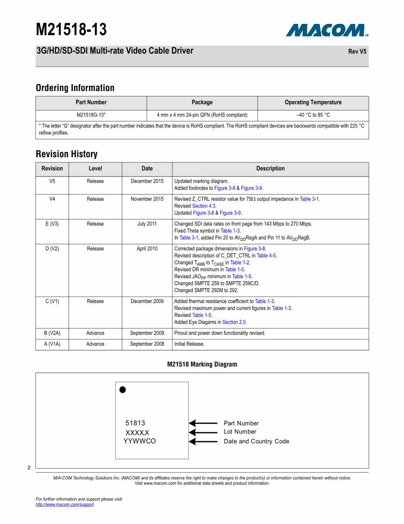
M21518 Marking Diagram
Part NumberLot Number
Date and Country Code XXXX.X
YYWWCO
51813
M21518-13
M/A-COM Technology Solutions Inc. (MACOM) and its affiliates reserve the right to make changes to the product(s) or information contained herein without notice. Visit www.macom.com for additional data sheets and product information.
For further information and support please visit:http://www.macom.com/support
2
3G/HD/SD-SDI Multi-rate Video Cable Driver Rev V5

M21518-13
3
3G/HD/SD-SDI Multi-rate Video Cable Driver Rev V5
Table of Contents
Ordering Information . . . . . . . . . . . . . . . . . . . . . . . . . . . . . . . . . . . . . . . . . . . . . . . . . . . . . . . . . . . . . . . . . . . . . . . . . . 2
Revision History. . . . . . . . . . . . . . . . . . . . . . . . . . . . . . . . . . . . . . . . . . . . . . . . . . . . . . . . . . . . . . . . . . . . . . . . . . . . . . 2
Table of Contents . . . . . . . . . . . . . . . . . . . . . . . . . . . . . . . . . . . . . . . . . . . . . . . . . . . . . . . . . . . . . . . . . . . . . . . . . . . . 3
1.0 Electrical Characteristics . . . . . . . . . . . . . . . . . . . . . . . . . . . . . . . . . . . . . . . . . . . . . . . . . . . . . . . . . . . . . . . . . . 4
2.0 Typical Performance Characteristics . . . . . . . . . . . . . . . . . . . . . . . . . . . . . . . . . . . . . . . . . . . . . . . . . . . . . . . . . 7
3.0 Pinout Diagram, Pin Description, and Package Drawing. . . . . . . . . . . . . . . . . . . . . . . . . . . . . . . . . . . . . . . . . . 8
4.0 Functional Description . . . . . . . . . . . . . . . . . . . . . . . . . . . . . . . . . . . . . . . . . . . . . . . . . . . . . . . . . . . . . . . . . . . 16
4.1 Block Diagram . . . . . . . . . . . . . . . . . . . . . . . . . . . . . . . . . . . . . . . . . . . . . . . . . . . . . . . . . . . . . . . . . . . . . . . . . . . . .164.2 Input Description. . . . . . . . . . . . . . . . . . . . . . . . . . . . . . . . . . . . . . . . . . . . . . . . . . . . . . . . . . . . . . . . . . . . . . . . . . .174.3 Output Description . . . . . . . . . . . . . . . . . . . . . . . . . . . . . . . . . . . . . . . . . . . . . . . . . . . . . . . . . . . . . . . . . . . . . . . . .184.4 Power Supply Description . . . . . . . . . . . . . . . . . . . . . . . . . . . . . . . . . . . . . . . . . . . . . . . . . . . . . . . . . . . . . . . . . . . .204.5 Logic Control Signals . . . . . . . . . . . . . . . . . . . . . . . . . . . . . . . . . . . . . . . . . . . . . . . . . . . . . . . . . . . . . . . . . . . . . . .22
4.5.1 Slew Rate Control (SD/xHD) . . . . . . . . . . . . . . . . . . . . . . . . . . . . . . . . . . . . . . . . . . . . . . . . . . . . . . . . . . . . . . . . . 224.5.2 Power Down Control . . . . . . . . . . . . . . . . . . . . . . . . . . . . . . . . . . . . . . . . . . . . . . . . . . . . . . . . . . . . . . . . . . . . . . . 224.5.3 Cable Detect Control . . . . . . . . . . . . . . . . . . . . . . . . . . . . . . . . . . . . . . . . . . . . . . . . . . . . . . . . . . . . . . . . . . . . . . . 224.5.4 Loss of Signal Control . . . . . . . . . . . . . . . . . . . . . . . . . . . . . . . . . . . . . . . . . . . . . . . . . . . . . . . . . . . . . . . . . . . . . . 23
M/A-COM Technology Solutions Inc. (MACOM) and its affiliates reserve the right to make changes to the product(s) or information contained herein without notice. Visit www.macom.com for additional data sheets and product information.
For further information and support please visit:http://www.macom.com/support

M21518-13
4
3G/HD/SD-SDI Multi-rate Video Cable Driver Rev V5
1.0 Electrical Characteristics
Unless noted otherwise, specifications apply for typical recommended operating conditions shown in Table 1-2, with AVDDO = 1.8 V, AVDDI = 1.2 V, CML inputs at 800 mV differential (RLOAD = 50 ), PRBS 210 – 1 test pattern at 2.97 Gbps.
Table 1-1. Absolute Maximum Ratings
Symbol Parameter Note Minimum Typical Maximum Unit
AVDDI Analog supply for input circuitry 1 -0.5 — 3.6 V
AVDDOA/B Analog supply for output circuitry 1 -0.5 — 3.6 V
TSTORE Storage Temperature 1 -65 — 150 °C
ESD Human Body Model (HBM) 1 -4 — 4 KV
ESD Charge Device Model (CDM) 1 -500 — 500 V
LU Latch Up @ 85 °C 1 -200 — 200 mA
HSIC Maximum High-speed input current 1 -100 — 100 mA
HSOC Maximum High-speed output short circuit current 1 -100 — 100 mA
VINMAX Input voltage range 1 -0.5 — AVDDI+0.5 V
NOTES:
1. Exposure to these conditions over extended periods of time may affect device reliability.
Table 1-2. Recommended Operating Conditions
Symbol Parameter Note Minimum Typical Maximum Unit
AVDDI Analog supply for input circuitry — 1.14 1.2, 1.8, 2.5, or 3.3
3.465 V
AVDDOA/B Analog supply for output circuitry — 1.71 1.8, 2.5, or 3.3
3.465 V
TCASE Ambient Operating temperature 1 -40 25 +85 °C
ESD Human Body Model (HBM) — -4 — 4 kV
NOTES:
1. Case temperature.
M/A-COM Technology Solutions Inc. (MACOM) and its affiliates reserve the right to make changes to the product(s) or information contained herein without notice. Visit www.macom.com for additional data sheets and product information.
For further information and support please visit:http://www.macom.com/support

M21518-13
5
3G/HD/SD-SDI Multi-rate Video Cable Driver Rev V5
Table 1-3. Power Consumption Specifications
Symbol Parameter Conditions Note Minimum Typical Maximum Unit
PTOTAL Total power consumption AVDDI = 1.2 V
AVDDO = 1.8 V
Both outputs enabled
1,3
—
52 83 mW
PTOTAL Total power consumption AVDDI = 1.2 V
AVDDO = 1.8 V
One output enabled
1,3
—
41 69 mW
I_ AVDDI Total AVDDI supply current AVDDI = 1.2 V 1,3 — 1 3 mA
I_ AVDDI Total AVDDI supply current AVDDI = 1.8 V 1,3 — 3 7 mA
I_ AVDDI Total AVDDI supply current AVDDI = 3.3 V 1,3 — 10 17 mA
I_ AVDDO Total AVDDO supply current Both outputs on 1,2,3 — 28 44 mA
I_ AVDDO Total AVDDO supply current One output on 1,2,3 — 22 36 mA
JA Junction to ambient Thermal Resistance
4 — 63 — °C/W
NOTES:
1. Recommended operating condition—see Table 1-2
2. Current consumption does not change with AVDDO = 1.8 V, 2.5 V or 3.3 V.
3. SD/xHD pin = 0.
4. Airflow = 0 m/s.
Table 1-4. Digital Input and Open Drain Output Specifications
Symbol Parameter Note Minimum Typical Maximum Unit
VIH Input Logic High — 0.85 x AVDDI — AVDDI + 0.5 V
VIF Input Logic Floating State — 0.25 x AVDDI — 0.75 x AVDDI V
VIL Input Logic Low — 0 — 0.15 x AVDDI V
IIH Input Current—Logic High — -100 — 100 µA
IIL Input Current—Logic Low — -100 — 100 µA
VOL Output Logic Low, IOL = 24 mA — — 0 0.2 x AVDDI V
M/A-COM Technology Solutions Inc. (MACOM) and its affiliates reserve the right to make changes to the product(s) or information contained herein without notice. Visit www.macom.com for additional data sheets and product information.
For further information and support please visit:http://www.macom.com/support

M21518-13
6
3G/HD/SD-SDI Multi-rate Video Cable Driver Rev V5
Table 1-5. High Speed Input/Output Electrical Specifications
Symbol Parameter Note Minimum Typical Maximum Unit
VO Output Voltage Range 1 730 800 850 mV
tR/tF SD Rise/Fall Time (20–80%) 1,3,4 400 600 800 ps
tR/tF 3G/HD Rise/Fall Time (20–80%) 1 — 70 90 ps
tR-tF SD Rise/Fall Time Mismatch 1,3,4 — — 125 ps
tR-tF 3G/HD Rise/Fall Time Mismatch 1,3 — — 30 ps
DCD Duty Cycle Distortion, SD 1,4 — — 100 ps
DCD Duty Cycle Distortion, 3G, HD 1,3 — — 30 ps
JAOPP Additive Output Jitter, SD 1,2,4 — 60 100 ps
JAOPP Additive Output Jitter, 3G, HD 1,2 — 12 29 ps
S22 Output Return Loss (5 MHz to 1.5 GHz) 6,8 20 — — dB
S22 Output Return Loss (5 MHz to 3.0 GHz) 5,8 11 — — dB
S22 Output Return Loss (5 MHz to 3.0 GHz) 6,8 14 — — dB
DR Input Data rate — 270 — 2970 Mbps
VID Differential Input Voltage (p–p) 7 400 — 1600 mV
VIC Input Common mode range — AVDDI – 0.6 — AVDDI + 0.1 V
IE Input Equalizer Gain Off (EN_EQ = 0) — — 0 — dB
Input Equalizer Gain Med (EN_EQ = F) — — 4 — dB
Input Equalizer Gain High (EN_EQ = H) — — 6 — dB
RINT Input Termination to AVDDI — 40 50 60
NOTES:
1. Measured AC coupled into 1 m coaxial cable, terminated with appropriate 75 or 50 load.
2. Measured with PRBS 215-1 test pattern.
3. For data rates above 360 Mbps, the cable driver must be in HD mode (SD/xHD = 0).
4. SD/xHD = 1, measured at 270 Mbps.
5. Without external matching network.
6. With external matching network Rmatching=75 , Lmatching=1nH, only applicable to 75 mode.
7. EQ_EN = L (input equalization off), point blank.
8. As measured on MACOM EVM at BNC connector with output impedance set to 75 .
M/A-COM Technology Solutions Inc. (MACOM) and its affiliates reserve the right to make changes to the product(s) or information contained herein without notice. Visit www.macom.com for additional data sheets and product information.
For further information and support please visit:http://www.macom.com/support

M21518-13
7
3G/HD/SD-SDI Multi-rate Video Cable Driver Rev V5
2.0 Typical Performance Characteristics
Figure 2-1. Eye Diagram at 270 Mbps Figure 2-2. Eye Diagram at 1485 Mbps
Figure 2-3. Eye Diagram at 2970 Mbps
M/A-COM Technology Solutions Inc. (MACOM) and its affiliates reserve the right to make changes to the product(s) or information contained herein without notice. Visit www.macom.com for additional data sheets and product information.
For further information and support please visit:http://www.macom.com/support
M21518-13
8
3G/HD/SD-SDI Multi-rate Video Cable Driver Rev V5
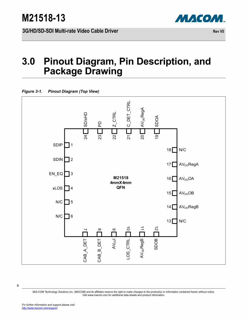
3.0 Pinout Diagram, Pin Description, and Package Drawing
Figure 3-1. Pinout Diagram (Top View)
M215184mmX4mm
QFN
SD
/xH
D2
4
PD
23
Z_
CT
RL
22
C_
DE
T_
CT
RL
21
AV
DDR
eg
A2
0
SD
OA
19
N/C18
AVDDRegA17
AVDDOA16
AVDDOB15
AVDDRegB14
N/C13
CA
B_
A_
DE
T
7
CA
B_
B_
DE
T
8
AV
DDI
9L
OS
_C
TR
L
10
AV
DDR
eg
B
11
SD
OB
12
SDIP 1
SDIN 2
EN_EQ 3
xLOS 4
N/C 5
N/C 6
M/A-COM Technology Solutions Inc. (MACOM) and its affiliates reserve the right to make changes to the product(s) or information contained herein without notice. Visit www.macom.com for additional data sheets and product information.
For further information and support please visit:http://www.macom.com/support

M21518-13
9
3G/HD/SD-SDI Multi-rate Video Cable Driver Rev V5
Table 3-1. Pin Description (1 of 2)
Pin Name Pin Number Type Description
AVSS Center Ground Paddle Power Chip Ground
AVDDI 9 Power Positive supply for input circuitry
AVDDRegA 17, 20 Power RegulatorA bypass capacitor connection, positive supply for outputA
AVDDRegB 11, 14 Power RegulatorB bypass capacitor connection, positive supply for outputB
AVDDOA 16 Power Positive supply for reglatorA
AVDDOB 15 Power Positive supply for reglatorB
SDOA 19 O-Analog High speed serial output A
SDOB 12 O-Analog High speed serial output B
SDIP/N 1,2 I-Analog High speed serial video data input
Z_CTRL 22 I-Analog Sets output impedance through an external Z_CTRL resistor connected to AVSS
Z_CTRL=665 to set 75 output impedanceZ_CTRL=250 to set 50 output impedance
SD/xHD 24 I-DIGITAL Output slew rate control
L = SDO has 3G/HD slew rateH = SDO has SD slew rate
CAB_A_DET 7 Open Drain Output with
internal 100k pull up
Cable Detect Output for Output A
L = Cable not detected on output AH = Cable detected on output A
CAB_B_DET 8 Open Drain Output with
internal 100k pull up
Cable Detect Output for Output B
L = Cable not detected on output BH = Cable detected on output B
PD 23 3-state/I-DIGITAL
Power down control
L = SDOA on, SDOB power downF = Both outputs on H = Power down both outputs
C_DET_CTRL 21 3-state/I-DIGITAL
Cable Detect Control
L = If any output is disconnected, device will be powered downF = Both outputs need to be disconnected for device to be powered downH = Power down upon cable detect disabled; cable detect outputs are active
LOS_CTRL 10 3-state/I-DIGITAL
Loss of Signal (LOS) control
L = LOS circuit disabledF = LOS circuit enabled; device powers down on LOSH = LOS circuit enabled; no power down on LOS
M/A-COM Technology Solutions Inc. (MACOM) and its affiliates reserve the right to make changes to the product(s) or information contained herein without notice. Visit www.macom.com for additional data sheets and product information.
For further information and support please visit:http://www.macom.com/support

M21518-13
10
3G/HD/SD-SDI Multi-rate Video Cable Driver Rev V5
EN_EQ 3 3-state/I-DIGITAL
Input equalization
L = No Input Equalization on SDIP/NF = Medium Input Equalization on SDIP/NH = High Input Equalization on SDIP/N
xLOS 4 Open Drain Output with
internal 100k pull up
Loss of input signal output (LOS)
L = Signal not presentH = Signal present
NOTES:
1. 3-state inputs have a default of F (floating).
2. A Z_CTRL resistance of 665 will also provide 800mVpp output swing.
Table 3-1. Pin Description (2 of 2)
Pin Name Pin Number Type Description
M/A-COM Technology Solutions Inc. (MACOM) and its affiliates reserve the right to make changes to the product(s) or information contained herein without notice. Visit www.macom.com for additional data sheets and product information.
For further information and support please visit:http://www.macom.com/support

M21518-13
11
3G/HD/SD-SDI Multi-rate Video Cable Driver Rev V5
Figure 3-2. Differential Input (SDIP, SDIN)
SDIP
AVDDI
AVSS
SDIN
AVDDI
AVSS
50Ω
50Ω
Input Buffer with Trace Equalizer
Figure 3-3. Single-Ended Output (SDOA, SDOB)
50Ω / 75ΩSet by Z _CTRL
SDO
AVDDReg
AVSS
M/A-COM Technology Solutions Inc. (MACOM) and its affiliates reserve the right to make changes to the product(s) or information contained herein without notice. Visit www.macom.com for additional data sheets and product information.
For further information and support please visit:http://www.macom.com/support

M21518-13
12
3G/HD/SD-SDI Multi-rate Video Cable Driver Rev V5
Figure 3-4. Digital Input Pin (SD/xHD)
INPUT
AVSS
2.0KΩ
AVDDI
Figure 3-5. 3-State Logic Input (PD, C_DET_CTRL, LOS_CTRL, EN_EQ)
AVSS
AVDDI
INPUT
AVDDI
AVSS
2.0KΩ
VREF_HIGH
AVSS
AVDDI
VREF_LOW
100KΩ
100KΩ
AVDDI
AVSS
M/A-COM Technology Solutions Inc. (MACOM) and its affiliates reserve the right to make changes to the product(s) or information contained herein without notice. Visit www.macom.com for additional data sheets and product information.
For further information and support please visit:http://www.macom.com/support
M21518-13
13
3G/HD/SD-SDI Multi-rate Video Cable Driver Rev V5
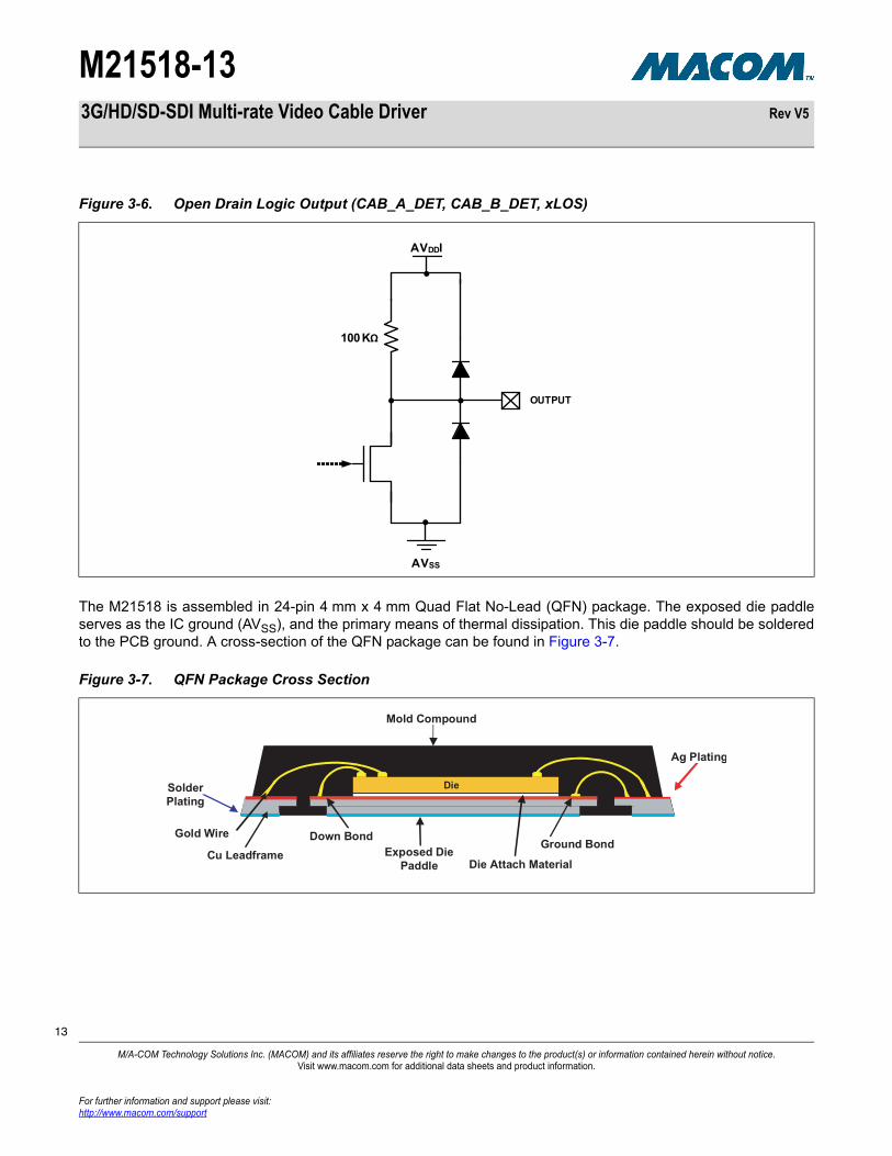
Figure 3-6. Open Drain Logic Output (CAB_A_DET, CAB_B_DET, xLOS)
AVDDI
AVSS
OUTPUT
100 KΩ
The M21518 is assembled in 24-pin 4 mm x 4 mm Quad Flat No-Lead (QFN) package. The exposed die paddle serves as the IC ground (AVSS), and the primary means of thermal dissipation. This die paddle should be soldered to the PCB ground. A cross-section of the QFN package can be found in Figure 3-7.
Figure 3-7. QFN Package Cross Section
Mold Compound
Gold Wire
Die Attach MaterialExposed Die
Paddle
Ground BondDown Bond
Cu Leadframe
SolderPlating
Ag Plating
Die
M/A-COM Technology Solutions Inc. (MACOM) and its affiliates reserve the right to make changes to the product(s) or information contained herein without notice. Visit www.macom.com for additional data sheets and product information.
For further information and support please visit:http://www.macom.com/support
M21518-13
14
3G/HD/SD-SDI Multi-rate Video Cable Driver Rev V5
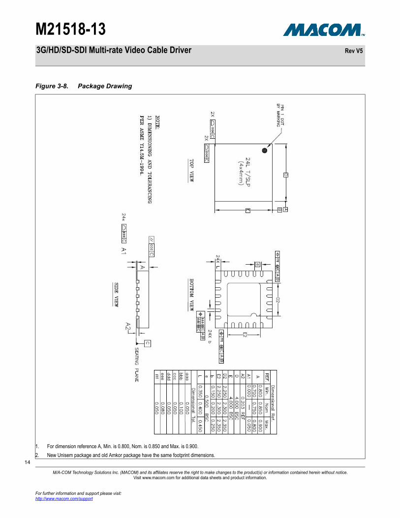
Figure 3-8. Package Drawing
1. For dimension reference A, Min. is 0.800, Nom. is 0.850 and Max. is 0.900.
2. New Unisem package and old Amkor package have the same footprint dimensions.
M/A-COM Technology Solutions Inc. (MACOM) and its affiliates reserve the right to make changes to the product(s) or information contained herein without notice. Visit www.macom.com for additional data sheets and product information.
For further information and support please visit:http://www.macom.com/support
M21518-13
15
3G/HD/SD-SDI Multi-rate Video Cable Driver Rev V5
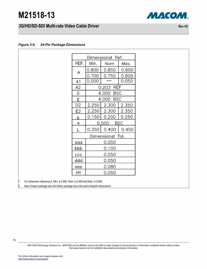
Figure 3-9. 24-Pin Package Dimensions
1. For dimension reference A, Min. is 0.800, Nom. is 0.850 and Max. is 0.900.
2. New Unisem package and old Amkor package have the same footprint dimensions.
M/A-COM Technology Solutions Inc. (MACOM) and its affiliates reserve the right to make changes to the product(s) or information contained herein without notice. Visit www.macom.com for additional data sheets and product information.
For further information and support please visit:http://www.macom.com/support
M21518-13
16
3G/HD/SD-SDI Multi-rate Video Cable Driver Rev V5
4.0 Functional Description
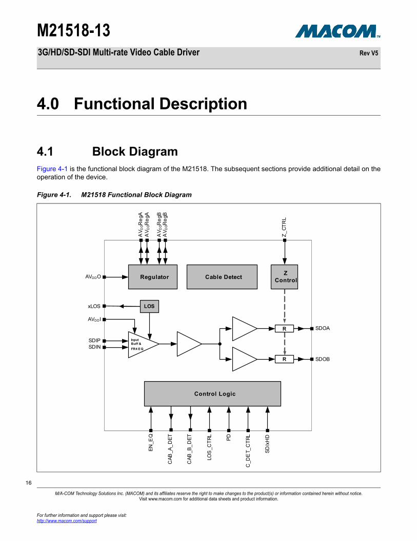
4.1 Block DiagramFigure 4-1 is the functional block diagram of the M21518. The subsequent sections provide additional detail on the operation of the device.
Figure 4-1. M21518 Functional Block Diagram
SDIPSDIN
AVDDI
Regulator Cable DetectZ
ControlZ
_C
TR
L
AV
DDR
egB
AV
DDR
egA
AV
DDR
egB
AV
DDR
egA
AVDDO
Input Buff &
FR4 EQ
SDOA
SDOB
R
R
Control Logic
C_D
ET_
CT
RL
PD
LOS
_CT
RL
CA
B_B
_D
ET
CA
B_A
_D
ET
EN
_EQ
LOSxLOS
SD
/xH
D
M/A-COM Technology Solutions Inc. (MACOM) and its affiliates reserve the right to make changes to the product(s) or information contained herein without notice. Visit www.macom.com for additional data sheets and product information.
For further information and support please visit:http://www.macom.com/support

M21518-13
17
3G/HD/SD-SDI Multi-rate Video Cable Driver Rev V5
4.2 Input DescriptionThe M21518 has a differential input, with integrated 50 pull-up resistors to AVDDI. AVDDI may be supplied from a 1.2 V, 1.8 V, 2.5 V, or 3.3 V supply. The input buffers are compatible with PCML, LVDS or LVPECL signal levels.
To improve signal integrity in large systems, the input has programmable input equalization (IE) with three gain levels: 0 dB, 4 dB, 6 dB.
Setting the gain to 0 dB effectively disables the IE feature. The pin EN_EQ allows for selecting the proper level of input equalization based on the board characteristics at the input. The maximum level of equalization compensates for up to 36” of FR4 trace. The operation of the EN_EQ pin is summarized in Table 4-1 below.
Table 4-1. Operation of EN_EQ Pin
Pin Level Function
EN_EQ L SDIP/N IE EQ gain = 0 dB
F SDIP/N IE EQ gain = 4 dB
H SDIP/N IE EQ gain = 6 dB
In 3G/HD/SD SDI applications, it is best to avoid AC coupling data interfaces between devices, if possible. DC coupling will result in increased system jitter margin. Also, DC coupling eliminates the requirement for additional components on the board. In order to accommodate DC coupling to the upstream device, the AVDDI domain of the M21518 is electrically isolated from all other power domains on chip. This allows for it to be tied to the VDD of the previous device’s output driver enabling a fully DC coupled system, as shown below.
Upstream M21518AVDDI1.2V – 3.3V VDD
5050
M/A-COM Technology Solutions Inc. (MACOM) and its affiliates reserve the right to make changes to the product(s) or information contained herein without notice. Visit www.macom.com for additional data sheets and product information.
For further information and support please visit:http://www.macom.com/support
M21518-13
18
3G/HD/SD-SDI Multi-rate Video Cable Driver Rev V5
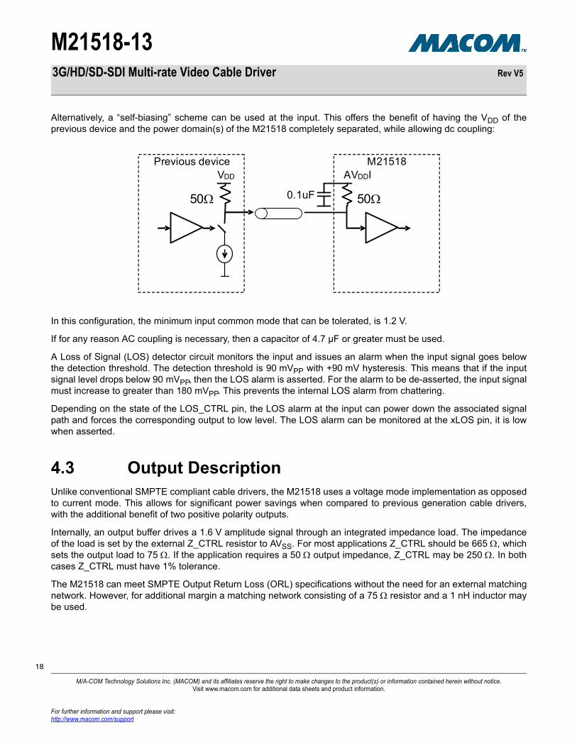
Alternatively, a “self-biasing” scheme can be used at the input. This offers the benefit of having the VDD of the previous device and the power domain(s) of the M21518 completely separated, while allowing dc coupling:
0.1uF
Previous device M21518AVDDIVDD
50 50
In this configuration, the minimum input common mode that can be tolerated, is 1.2 V.
If for any reason AC coupling is necessary, then a capacitor of 4.7 µF or greater must be used.
A Loss of Signal (LOS) detector circuit monitors the input and issues an alarm when the input signal goes below the detection threshold. The detection threshold is 90 mVPP with +90 mV hysteresis. This means that if the input signal level drops below 90 mVPP, then the LOS alarm is asserted. For the alarm to be de-asserted, the input signal must increase to greater than 180 mVPP. This prevents the internal LOS alarm from chattering.
Depending on the state of the LOS_CTRL pin, the LOS alarm at the input can power down the associated signal path and forces the corresponding output to low level. The LOS alarm can be monitored at the xLOS pin, it is low when asserted.
4.3 Output DescriptionUnlike conventional SMPTE compliant cable drivers, the M21518 uses a voltage mode implementation as opposed to current mode. This allows for significant power savings when compared to previous generation cable drivers, with the additional benefit of two positive polarity outputs.
Internally, an output buffer drives a 1.6 V amplitude signal through an integrated impedance load. The impedance of the load is set by the external Z_CTRL resistor to AVSS. For most applications Z_CTRL should be 665 , which sets the output load to 75 . If the application requires a 50 output impedance, Z_CTRL may be 250 . In both cases Z_CTRL must have 1% tolerance.
The M21518 can meet SMPTE Output Return Loss (ORL) specifications without the need for an external matching network. However, for additional margin a matching network consisting of a 75 resistor and a 1 nH inductor may be used.
M/A-COM Technology Solutions Inc. (MACOM) and its affiliates reserve the right to make changes to the product(s) or information contained herein without notice. Visit www.macom.com for additional data sheets and product information.
For further information and support please visit:http://www.macom.com/support

M21518-13
19
3G/HD/SD-SDI Multi-rate Video Cable Driver Rev V5
The device has a power down pin, PD. The operation of the PD pin is summarized in Table 4-2 below. When only SDOB is powered down, the signal at SDOB is set to low. When both SDOA and SDOB are powered down, both outputs are high impedance.
Table 4-2. Operation of PD Pin
Pin Level Function
PD L SDOA on, SDOB powered down
F Both SDOA and SDOB on
H Both SDOA and SDOB powered down
Figure 4-2 shows a typical output circuit.
When the cable detect function is enabled, only the outputs used need to be connected, while unused outputs may be left floating. However, if the cable detection function is disabled, the unused output must be powered down or properly terminated. When SDOB only is powered down, SDOB output will be approximately 75 to ground. When both SDOA and SDOB are powered down, both outputs will be high impedance
Figure 4-2. Typical Output Circuit (all Outputs Connected)
M21518
SDOA
SDOB
4.7 µF
4.7 µF
M/A-COM Technology Solutions Inc. (MACOM) and its affiliates reserve the right to make changes to the product(s) or information contained herein without notice. Visit www.macom.com for additional data sheets and product information.
For further information and support please visit:http://www.macom.com/support

M21518-13
20
3G/HD/SD-SDI Multi-rate Video Cable Driver Rev V5
4.4 Power Supply DescriptionThe device features two internal regulators to supply the power for the drivers for each output. AVDDOA and AVDDOB supply the voltage to each output’s respective regulator. These pins may be connected to DC voltages ranging from 1.8 V to 3.3 V. Each regulator pin requires an external 1 µF bypass capacitor to ground, which must be connected to AVDDRegA and to AVDDRegB. It is recommended to add a secondary 10 nF bypass capacitor on each regulator output as close to pin as possible.
In addition to supplying the output stage for SDOB, AVDDOB is also used to power the core circuitry.
A completely separate supply domain, AVDDI, provides the supply for the high-speed serial input pins. The input termination and ESD protection for the SDI pins and the digital control input pins are referenced to this supply. The isolated domain allows DC coupling to an upstream device that is running from a different supply voltage. For example, if, in order to save power, AVDDOA/B are connected to 1.8 V, but the cable driver must interface to a reclocker that uses a 3.3 V supply, then DC coupling can be achieved by simply connecting AVDDI to the 3.3 V rail.
Figure 4-3 to 4-5 show three examples of how the cable driver can be configured. Note that even when only one output is enabled, both output regulators must be supplied with the correct voltage.
Figure 4-3. Supply Configuration, Both A and B Outputs Used
1.2V to 3.3V
AVDDRegA
AVDDRegB
AVDDI
1µF
1µF
0.1uF
PD
1.8V to 3.3V
AVDDOB
AVDDOA
10 nF
10 nF
0.1uF
M/A-COM Technology Solutions Inc. (MACOM) and its affiliates reserve the right to make changes to the product(s) or information contained herein without notice. Visit www.macom.com for additional data sheets and product information.
For further information and support please visit:http://www.macom.com/support

M21518-13
21
3G/HD/SD-SDI Multi-rate Video Cable Driver Rev V5
Figure 4-4. Supply Configuration, Output A Used, Output B Powered Down
1.2V to 3.3V
1.8V to 3.3V
0.1uF
AVDDRegA
AVDDOB
AVDDRegB
AVDDI
1µF
1µF
PD
AVDDOA
10 nF
10 nF
Figure 4-5. Supply Configuration, Power Down Mode
1.2V to 3.3V
AVDDRegA
AVDDRegB
AVDDI
1µF
1µF0.1uF
PD
1.8V to 3.3V
AVDDOB
AVDDOA
10 nF
10 nF
0.1uF
M/A-COM Technology Solutions Inc. (MACOM) and its affiliates reserve the right to make changes to the product(s) or information contained herein without notice. Visit www.macom.com for additional data sheets and product information.
For further information and support please visit:http://www.macom.com/support

M21518-13
22
3G/HD/SD-SDI Multi-rate Video Cable Driver Rev V5
4.5 Logic Control SignalsThe digital logic control signals are ESD protected and referenced to the AVDDI. This allows the device to interface to many different logics levels from different supply domains.
Some pins have a state called "F"; this stands for "floating." To assert this state leave the pin unconnected or undriven.
4.5.1 Slew Rate Control (SD/xHD)Pin SD/xHD controls the slew rate of the high-speed output. To comply with the SMPTE specification the slew rate is slowed down to approximately 600 ps when in SD mode. Note that there is no pull-up on the SD/xHD pin, so it should not be left floating.
Table 4-3. Slew Rate Control (SD/xHD)
Pin Level Function
SD/xHD L Set SDOA/B Slew rate to 3G/HD Levels
H Set SDOA/B Slew rate to SD Levels
4.5.2 Power Down ControlThe PD pin can be used to power down one or both of the M21518 high-speed outputs. This control is independent of the cable detect and LOS power down controls.
Table 4-4. Operation of PD Pin
Pin Level Function
PD L SDOA on, SDOB powered down
F Both outputs on
H Power down both outputs
4.5.3 Cable Detect ControlThe M21518 features an integrated near-end cable detector. This circuit can detect whether a cable has been disconnected from an output and whether or not it is reconnected without requiring any additional external components.
Utilizing the cable detection feature has several system level advantages such as:
• Reduced power consumption when no cable is connected to both outputs
• Reduced EMI
• Eliminates the requirement for external termination
M/A-COM Technology Solutions Inc. (MACOM) and its affiliates reserve the right to make changes to the product(s) or information contained herein without notice. Visit www.macom.com for additional data sheets and product information.
For further information and support please visit:http://www.macom.com/support

M21518-13
23
3G/HD/SD-SDI Multi-rate Video Cable Driver Rev V5
If C_DET_CTRL pin = 'L' and either output A or B are disconnected, the device will automatically power down. IfC_DET_CTRL pin = 'F' and both output A and B are disconnected, the device will automatically power down. In both cases the resulting power reduction is 50%.
Table 4-5. Cable Detection Functions
Pin Level Function
C_DET_CTRL L Powers down if any active output is disconnected.
F Powers down if all active outputs are disconnected.
H Power down disabled, but CAB_A_DET is active and if SDOB is enabled then CAB_B_DET is also active.
There are two cable detection outputs (CAB_A_DET and CAB_B_DET). These are always active and go to a logic low when SDOA and SDOB respectively are disconnected from a cable or matched load.
The cable detection power down function may be disabled by setting C_DET_CTRL = H. In this state CAB_A_DET and CAB_B_DET are still active.
4.5.4 Loss of Signal ControlAs mentioned in Section 4.2, the M21518 features a Loss of Signal monitor on the high speed data input.
The LOS_CTRL pin controls this function as detailed in Table 4-6.
Table 4-6. Loss of Signal Control
Pin Level Function
LOS_CTRL L LOS circuit is disabled, xLOS output fixed high
F xLOS output active, power down on LOS assert
H xLOS output active, no power down on LOS assert
M/A-COM Technology Solutions Inc. (MACOM) and its affiliates reserve the right to make changes to the product(s) or information contained herein without notice. Visit www.macom.com for additional data sheets and product information.
For further information and support please visit:http://www.macom.com/support
M/A-COM Technology Solutions Inc. All rights reserved.
Information in this document is provided in connection with M/A-COM Technology Solutions Inc ("MACOM") products. These materials are provided by MACOM as a service to its customers and may be used for informational purposes only. Except as provided in MACOM's Terms and Conditions of Sale for such products or in any separate agreement related to this document, MACOM assumes no liability whatsoever. MACOM assumes no responsibility for errors or omissions in these materials. MACOM may make changes to specifications and product descriptions at any time, without notice. MACOM makes no commitment to update the information and shall have no responsibility whatsoever for conflicts or incompatibilities arising from future changes to its specifications and product descriptions. No license, express or implied, by estoppel or otherwise, to any intellectual property rights is granted by this document.
THESE MATERIALS ARE PROVIDED "AS IS" WITHOUT WARRANTY OF ANY KIND, EITHER EXPRESS OR IMPLIED, RELATING TO SALE AND/OR USE OF MACOM PRODUCTS INCLUDING LIABILITY OR WARRANTIES RELATING TO FITNESS FOR A PARTICULAR PURPOSE, CONSEQUENTIAL OR INCIDENTAL DAMAGES, MERCHANTABILITY, OR INFRINGEMENT OF ANY PATENT, COPYRIGHT OR OTHER INTELLECTUAL PROPERTY RIGHT. MACOM FURTHER DOES NOT WARRANT THE ACCURACY OR COMPLETENESS OF THE INFORMATION, TEXT, GRAPHICS OR OTHER ITEMS CONTAINED WITHIN THESE MATERIALS. MACOM SHALL NOT BE LIABLE FOR ANY SPECIAL, INDIRECT, INCIDENTAL, OR CONSEQUENTIAL DAMAGES, INCLUDING WITHOUT LIMITATION, LOST REVENUES OR LOST PROFITS, WHICH MAY RESULT FROM THE USE OF THESE MATERIALS.
MACOM products are not intended for use in medical, lifesaving or life sustaining applications. MACOM customers using or selling MACOM products for use in such applications do so at their own risk and agree to fully indemnify MACOM for any damages resulting from such improper use or sale.
M21518-13
24
3G/HD/SD-SDI Multi-rate Video Cable Driver Rev V5