m08889 high performance rgb driver for … sheets/ma-com...08889-dsh-001-g mindspeed technologies ®...
TRANSCRIPT
08889-DSH-001-G Mindspeed Technologies® February 2012Mindspeed Proprietary and Confidential
M08889High Performance RGB Driver for DLP/LCD/LCoS Projectors
Features• Three 2 A common anode LED/laser drivers • Integrated 12.5 Msps 10-bit current DACs with 6-bit programmable
full scale• Real-time continuous and integrating optical power control • Synchronous Buck-Boost DC-DC converter with typical efficiency of
88% for 1.5 A output current with input voltage from 2.7 V to 5 V• Safety circuitry• High speed I2C interface
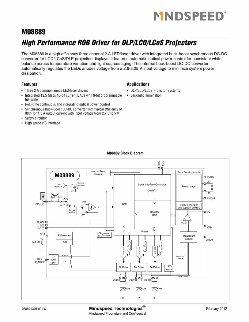
The M08889 is a high efficiency three channel 2 A LED/laser driver with integrated buck-boost synchronous DC-DC converter for LCD/LCoS/DLP projection displays. It features automatic optical power control for consistent white balance across temperature variation and light sources aging. The internal buck-boost DC-DC converter automatically regulates the LEDs anodes voltage from a 2.6-5.25 V input voltage to minimize system power dissipation.
M08889 Block DiagramS
DA SCL
Serial Interface Controller
Dual I2C
Internal Temp Sensor
I0_ONI1_ONI2_ON
M08889
R/G/B R/G/B R/G/B
10-b
it D
AC
2A Driver2A Driver 2A Driver
10-b
it D
AC
Headroom control
VLDD monitor
Internal oscillator
10-b
it D
AC
6-bi
tS
cale
DA
C
6-bi
tS
cale
DA
C
6-bi
tS
cale
DA
C
APC
Timers
Register table
IOUT0 IOUT1 IOUT2
LEDAlarm
13-bit Target DAC
CPC
IPC
Current scaling
VREF
C
CurrentComparator
PDAPC_IN
Vref References
POR12.4 kΩ
DIS/LP_MODE
3 level pin
LP Mode
DIS
PVDD
Headroom Control
Buck Boost converter
VREF
VC
PWM generatorand support circuitry
VFB
VIOUT
PVOUT
Power stage
LR
LL
Applications• DLP/LCD/LCoS Projector Systems• Backlight illumination

ConventionsThroughout this document an italic x is used to indicate different channels; i.e. IOUTx means IOUT0, IOUT1, or IOUT2.
Ordering InformationPart Number Package Operating Temperature
M08889G-13 * 36 pin, 6 mm x 5 mm QFN -40 °C to +85 °C
M08889-13EVM Evaluation board with M08889-12 -40 °C to +85 °C
* The letter “G” designator in the part number indicates that the device is RoHS-compliant. Refer to www.mindspeed.com for additional information.
Revision HistoryRevision Level Date Description
G Release February 2012 Table 1-1: PVDD, PVOUT, LL, LR, VFB and VC absolute maximums.
Table 1-2: LVPOR and HVPOR specifications.
Table 1-3: PVDD, PVOUT, tr_PVOUT and Overvoltage specifications.
Added Figure 1-1.
Table 1-8: IOUTx output stability specification.
Table 1-11: Headroom Variation specification.
Table 3-1: Recommended register settings changed.
F Preliminary December 2011 “M08889 Block Diagram” on page 1, removed 4-wire serial interface.
Table 1-1: Removed I2C/SPI.
Section 1.9: Corrected I2C address (changed 4Ch, 98h, and 99h to 4Dh, 9Ah, and 9Bh, respectively).
Table 3-1: Added settings for registers 0x03, 0x1F, 0x22, 0x61, 0x62, 0x63, and 0x64.
E Preliminary October 2011 Update registers and functional description for -13 revision of part.
D Preliminary August 2011 Updated Application Drawing on page 3.
Added clarifying text to Register.alarm_iout (address.83h).
C Preliminary August 2011 Added Register Section. Update specifications, descriptions and applications information.
B Preliminary July 2011 Change package pinout. Add Application Drawing.
A Preliminary February 2011 Initial
08889-DSH-001-G Mindspeed Technologies®2
Mindspeed Proprietary and Confidential
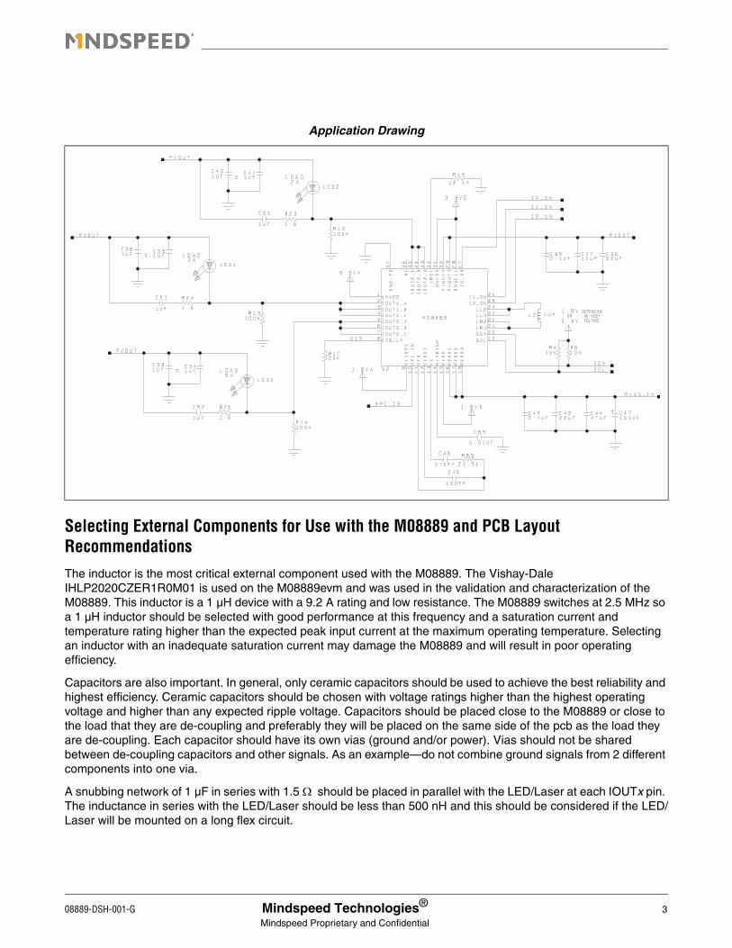
Selecting External Components for Use with the M08889 and PCB Layout RecommendationsThe inductor is the most critical external component used with the M08889. The Vishay-Dale IHLP2020CZER1R0M01 is used on the M08889evm and was used in the validation and characterization of the M08889. This inductor is a 1 µH device with a 9.2 A rating and low resistance. The M08889 switches at 2.5 MHz so a 1 µH inductor should be selected with good performance at this frequency and a saturation current and temperature rating higher than the expected peak input current at the maximum operating temperature. Selecting an inductor with an inadequate saturation current may damage the M08889 and will result in poor operating efficiency.
Capacitors are also important. In general, only ceramic capacitors should be used to achieve the best reliability and highest efficiency. Ceramic capacitors should be chosen with voltage ratings higher than the highest operating voltage and higher than any expected ripple voltage. Capacitors should be placed close to the M08889 or close to the load that they are de-coupling and preferably they will be placed on the same side of the pcb as the load they are de-coupling. Each capacitor should have its own vias (ground and/or power). Vias should not be shared between de-coupling capacitors and other signals. As an example—do not combine ground signals from 2 different components into one via.
A snubbing network of 1 µF in series with 1.5 Ω should be placed in parallel with the LED/Laser at each IOUTx pin. The inductance in series with the LED/Laser should be less than 500 nH and this should be considered if the LED/Laser will be mounted on a long flex circuit.
Application Drawing
08889-DSH-001-G Mindspeed Technologies®3
Mindspeed Proprietary and Confidential

Basic M08889 Register Set-upIn most applications only a small number of registers need to be written at power-up. These same registers will also need to be rewritten after the disable pin (DIS) is cycled. Whenever it is desired that the LED/Laser currents change the ioutx_msb and/or ioutx_lsb will need to be rewritten and the new values will be strobed into the output DACs on the low to high transition of the corresponding Ix_ON pin.
See the appropriate section in the Functional Description chapter of this data sheet if advanced features of the M08889 are used. These advanced features include Automatic Power Control of outputs using a photodiode or color sensor, Timer-modulated output currents, Low Power Mode and Output Alarm configurations. The registers used for each of these functions will be listed in the appropriate section and a complete listing of the M08889 registers is included at the last section of this data sheet.
Basic Register Configuration (all other registers may be left at their default value)
Name Address RecommendSetting Description
opmode_ctrl0 0x00 50h Enable self-calibration of pin.IOUTx headroom.
opmode_ctrl1 0x01 80h or 90h Recommended setting.
reserved 0x03 80h Disable DC-DC speed-up circuit.
out_ctrlx 0x05, 0x06, 0x07 7Fh Recommended DC-DC feedback setting.
tempsens_ctrl 0x08 22h Recommended temperature sensor configuration.
ioutx_msb 0x10[1:0], 0x14[1:0], 0x18[1:0]
xxb Two most significant bits of output current setting.
ioutx_lsb 0x11, 0x15, 0x19 xxh Eight least significant bits of output current setting.
ioutx_scale 0x12, 0x16, 0x1A 00xxxxxb Set the scaling of the output currents.
DC-DC_overvoltage 0x1F A0h Set DC-DC overvoltage protection to 5 V nominal.
DC-DC_mode 0x20 03h Recommended DC-DC converter configuration.
reserved 0x22 40 Recommended DC-DC converter configuration.
regref_setup 0x24 20h Recommended DC-DC converter feedback configuration.
regrefx_ctrl1 0x27, 0x2B, 0x2F 3Fh57h7FhAFh
Output headroom and decimation factor for pin.IOUTx current less than 0.6 A.
Output headroom and decimation factor for pin.IOUTx current from 0.6 A to 1 A.
Output headroom and decimation factor for pin.IOUTx current from 1 A to 1.5 A.
Output headroom and decimation factor for pin.IOUTx current from 1.5 A to 2.0 A.
regrefx_ctrl0 0x28, 0x2C, 0x30 44h Recommended DC-DC converter configuration.
DCDC_ctrl3 0x61 15h, then write 95h to this
register after 01h is written to 0x72.
Recommended DC-DC negative current limit (set to 7 A).
DCDC_ctrl2 0x62 2Fh Enable overvoltage protection and set positive current limit (set to 7 A).
DCDC_ctrl1 0x63 8Fh Enable internal DC-DC feedback.
DCDC_ctrl0 0x64 5Fh Recommended DC-DC converter configuration.
start_op 0x72 01h Register loading complete, begin operation.
08889-DSH-001-G Mindspeed Technologies®4
Mindspeed Proprietary and Confidential
08889-DSH-001-G
1.0 Electrical Characteristics
1.1 Absolute Maximum RatingsThese are the absolute maximum ratings at or beyond which the IC can be expected to fail or be damaged. Reli-able operation at these extremes for any length of time is not implied.
Table 1-1. Absolute Maximum Ratings
Symbol Parameter Minimum Typical Maximum Units
DVDD, ALVDD 1.8 V digital and analog supplies — 1.98 — V
DHVDD, AHVDD 3.3 V digital and analog supplies — 3.63 — V
PVDD Voltage supply to power DC-DC converter — 5.25 — V
PVOUT DC-DC converter output pin — 5.25 — V
LL, LR External inductor pins for DC-DC converter — 5.5 — V
IOUT0, IOUT1, IOUT2 Output pins for driving LED/Laser - maximum voltage — 5.5 — V
TJCTN Junction temperature -40 — +125 °C
TSTG Storage temperature -65 — +150 °C
APC_IN RGB photodiode feedback input voltage -0.4 — ALVDD + 0.4 V
VFB DC-DC converter feedback pin — 3.63 — V
IAPC_IN RGB photodiode feedback input current -0.5 — 4 mA
I_VREF Current into reference voltage pin -0.12 — +0.12 mA
DIS/LP_MODE Disable all LED/Laser outputs or operate with low power values -0.4 — 3.63 V
I0_ON, I1_ON, I2_ON Input pins to activate LED/Laser output -0.4 — 3.63 V
SCLK_S, SDA_S I2C interface -0.4 — 3.63 V
VC — 3.63 — V
Mindspeed Technologies®5
Mindspeed Proprietary and Confidential

1.2 DC CharacteristicsMin and Max values: Tc= -40 °C to 85 °C, DVDD=1.8 V+/-5%, ALVDD=1.8 V+/-5%, DHVDD=3.3 V+/-5%,
AHVDD =3.3 V+/-5% unless otherwise noted. Typical values: Tc=25 °C, DVDD=1.8 V, ALVDD=1.8 V, DHVDD =3.3 V, AHVDD =3.3 V unless otherwise noted.
Table 1-2. DC Characteristics LED Driver
Symbol Parameter Notes Minimum Typical Maximum Units
DVDD 1.8 V supply for digital circuitry — 1.71 1.8 1.89 V
ALVDD 1.8 V supply for analog circuitry — 1.71 1.8 1.89 V
DHVDD 3.3 V supply for digital circuitry — 3.13 3.3 3.47 V
AHVDD 3.3 V supply for analog circuitry — 3.13 3.3 3.47 V
ILVDD 1.8 V supply current
(DVDD and ALVDD)
1, 2, 3, 4 — — 7 mA
Standby current - 1.8 V — — 0.001 —
IHVDD 3.3 V supply current
(DHVDD and AHVDD)
1, 3, 4 — — 0.12 mA
Standby current - 3.3 V — — 0.001 —
PVDD Standby current — — 1 — µA
LVPOR Power-on RESET voltage for 1.8 V supply
De-assert (rising voltage on 1.8 V supply) — — 1.5 — V
Assert (falling voltage on 1.8 V supply) — — 1.4 —
HVPOR Power-on RESET voltage for 3.3 V supply
De-assert (rising voltage on 3.3 V supply) — — 2.7 — V
Assert (falling voltage on 3.3 V supply) — — 2.65 —
TC Case temperature 5 -40 — 85 °C
NOTES:1. Excludes I2C serial interface current and LED current.
2. ILVDD will be increase by 0.5% of the Ix_OUT current when Ix_OUT is active.
3. Operating in IPC or CPC will add less than 1 mA current over Open Loop mode.
4. Open Loop with default register values loaded after RESET.
5. Measured on top of M08889 case
Table 1-3. DC Characteristics DC-DC Converter
Symbol Parameter Notes Minimum Typical Maximum Units
PVDD Voltage input to DC-DC converter 1 2.7 — 5 V
2 3.3 — 5 V
PVOUT DC-DC converter output voltage 3 — — 5 V
VFB DC-DC converter feedback voltage — — 1.24 — V
CPVDD Minimum DC-DC converter input capacitance — 170 — — µF
ηDC-DC DC-DC converter efficiency 4 — 88 %
08889-DSH-001-G Mindspeed Technologies®6
Mindspeed Proprietary and Confidential

tr_PVOUT System risetime of PVOUT and IOUTx 5 — 20 — µs
VOVER Overvoltage 6 4.8 5 5.3 V
NOTES:1. 1.5 A Output Current.
2. 2 A Output Current.
3. Operation below 2.2 V not recommended.
4. Typical operating conditions, 2.7 V to 5 V input voltage, 1.5 A output current.
5. Schematic as shown in Chapter 1. Red LED output voltage to Green output voltage, all operating temperatures and currents.
6. Register 1Fh=A0h.
Figure 1-1. DC-DC and Output Driver System Efficiency at 3/4 Scale Output Current (1.5 A nominal)
Table 1-3. DC Characteristics DC-DC Converter
Symbol Parameter Notes Minimum Typical Maximum Units
0
25
50
75
100
0 1 2 3 4 5 6
Red LED Output Efficiency vs PVDD
Eff icien
cy (%
)
PVDD (V)
0
25
50
75
100
0 1 2 3 4 5 6
Blue LED Output Efficiency vs PVDDEff icien
cy (%
)
PVDD (V)
0
25
50
75
100
0 1 2 3 4 5 6
Green LED Output Efficiency vs PVDD
Efficiency (%
)
PVDD (V)
08889-DSH-001-G Mindspeed Technologies®7
Mindspeed Proprietary and Confidential

1.3 APC CharacteristicsMin and Max values: Tc= -40 °C to 85 °C, DVDD=1.8 V+/-5%, ALVDD=1.8 V+/-5%, DHVDD=3.3 V+/-5%,
AHVDD =3.3 V+/-5% unless otherwise noted. Typical values: Ta=25 °C, DVDD, ALVDD=1.8 V, AHVDD =3.3 V
Table 1-4. APC Input Characteristics (Current Source Input)
Parameter Notes Minimum Typical Maximum Units
Full scale input 1 — 3 — mA
PD capacitance 1, 2 — — 80 pF
Input bias 1 ALVDD/2 — — V
Maximum input voltage — — — 1.89 V
NOTES:1. APC_IN pin.
2. Care should be taken in routing of each PD input so that total capacitance on the pin including routing does not exceed 80 pF
Table 1-5. APC Input Characteristics (Current Sink Input)
Parameter Notes Minimum Typical Maximum Units
Full scale input 1 — 3.25 — mA
PD capacitance1 1, 2 — — 300 pF
Min input bias 1 — 0.6 — V
Maximum input voltage — — — 1.89 V
NOTES:1. APC_IN pin.
2. Care should be taken in routing of each PD input so that total capacitance on the pin including routing does not exceed 300 pF
Table 1-6. CPC Target DAC
Parameter Notes Minimum Typical Maximum Units
Resolution — — 13 — bits
Conversion rate — — 30 — Msps
Full scale monitor photodetector current — — 3.25 3.4 mA
Step size — — 350 515 nA
CPC control loop accuracy 1 -8.5 — 8.5 %
NOTES:1. At Tc= 120 °C control loop accuracy is +/-7%
08889-DSH-001-G Mindspeed Technologies®8
Mindspeed Proprietary and Confidential

1.4 LED DriversMin and Max values: Tc= -40 °C to 85 °C, DVDD=1.8 V+/-5%, ALVDD=1.8 V+/-5%, DHVDD=3.3 V+/-5%,
AHVDD =3.3 V+/-5% unless otherwise noted. Typical values: Tc=25 °C, DVDD, ALVDD=1.8 V, AHVDD =3.3 V
Table 1-7. Integrating Power Control
Parameter Notes Minimum Typical Maximum Units
Resolution — — 10 — bits
Count variation (part to part) — -35 +35 %
Stability 2, 3 -11 — +11 %
NOTES:1. This will correspond to a total optical power variation: monotonicity will still be guaranteed by the architecture.
2. For targets > xxx µA and address 0x0B=50h
3. Variation of integration target over supply and temperature. At Tc= 120 °C accuracy is +/-14%
Table 1-8. LED Drivers
Parameter Conditions Notes Minimum Typical Maximum Units
IOUTx current at maximum setting
Maximum output current setting (ioutx_msb=11b, ioutx_lsb = FFh, ioutx_scale=3Fh), programmed for 200 mV headroom (regrefx_ctrl1=10100xxxb). Note that the measured headroom at the pin will subject to headroom setting accuracy and resistances of the bondwire, solder connection and pcb trace.
— 1.80 1.95 2.10 A
IOUTx current at 3/4 of maximum setting
Output current setting (ioutx_msb=10b, ioutx_lsb = FFh, ioutx_scale=3Fh), programmed for 150 mV headroom (regrefx_ctrl1=01111xxxb). Note that the measured headroom at the pin will subject to headroom setting accuracy and resistances of the bondwire, solder connection and pcb trace.
— 1.34 1.45 1.56 A
IOUTx current at 1/2 of maximum setting
Output current setting (ioutx_msb=01b, ioutx_lsb = FFh, ioutx_scale=3Fh), programmed for 100 mV headroom (regrefx_ctrl1=01010xxxb). Note that the measured headroom at the pin will subject to headroom setting accuracy and resistances of the bondwire, solder connection and pcb trace.
— 0.88 0.96 1.04 A
IOUTx current at 1/4 of maximum setting
Output current setting (ioutx_msb=00b, ioutx_lsb = FFh, ioutx_scale=3Fh), programmed for 70 mV headroom (regrefx_ctrl1=00111xxxb). Note that the measured headroom at the pin will subject to headroom setting accuracy and resistances of the bondwire, solder connection and pcb trace.
— 0.43 0.47 0.51 A
IOUTx leakage current 5 V bias voltage at pin IOUTx. Ix_ON low — — 25 — µA
IOUTx output stability IOUTx current over temperature and voltage for constant output setting and constant headroom setting, 1/4 to Full Scale output using recommended headroom settings in Chapter 3.
— -3 +3 %
08889-DSH-001-G Mindspeed Technologies®9
Mindspeed Proprietary and Confidential

Maximum allowable IOUTx voltage headroom
2 — — 5.25 V
Rise/fall time 20-80% Into 1 Ω electrical output, no snubber network 3 — — 200 ns
NOTES:1. Required headroom scales with output current, maximum output current requires maximum headroom (see Section 3.4.2).
2. To prevent damage at output pins do not exceed this voltage. Also verify power sequencing and power dissipation.
3. Guaranteed by design
Table 1-9. Output Current DACs
Parameter Notes Minimum Typical Maximum Units
Resolution — — 10 — bits
Conversion rate — — 12.5 — Msps
Full scale IOUTx 1 — 2 — A
IOUTx absolute accuracy 1, 2 -8 — +8 %
NOTES:1. Referred to the current output
2. For driver headroom > value specified in Table 3-1. Measured at 1000 mA.
Table 1-10. Scale DACs
Parameter Notes Minimum Typical Maximum Units
Resolution — — 6 — bits
Minimum scale value (referred to the current output, equivalent to code 000000b) — — 200 — mA
Maximum scale value (referred to the current output, equivalent to code 111111b) — — 2 — A
Scale step (referred to the current output) — — 28.6 — mA
Table 1-8. LED Drivers
Parameter Conditions Notes Minimum Typical Maximum Units
08889-DSH-001-G Mindspeed Technologies®10
Mindspeed Proprietary and Confidential
1.5 DC-DC Converters Reference GeneratorsMin and Max values: Tc= -40 °C to 85 °C, DVDD=1.8 V+/-5%, ALVDD=1.8 V+/-5%, DHVDD=3.3 V+/-5%,
AHVDD =3.3 V+/-5% unless otherwise noted. Typical values: Tc=25 °C, DVDD, ALVDD=1.8 V, AHVDD =3.3 V
1.6 Internal Temperature SensorTypical values: Tc=25 °C, DVDD, ALVDD=1.8 V, AHVDD =3.3 V
1.7 Light Sources AlarmMin and Max values: Tc= -40 °C to 85 °C, DVDD=1.8 V+/-5%, ALVDD=1.8 V+/-5%, DHVDD=3.3 V+/-5%, AHVDD =3.3 V+/-5% unless otherwise noted.
Typical values: Tc=25 °C, DVDD, ALVDD=1.8 V, AHVDD =3.3 V
Table 1-11. DC-DC Converters Reference Generators
Parameter Notes Minimum Typical Maximum Units
Voltage compliance — 0.5 1.2 1.3 V V
DAC resolution — — 9 — bits
DAC DNL — -0.5 — 0.5 LSB
DAC full scale (regref_setup[1]=0b) — — 100 — µA
DAC full scale (regref_setup[1]=1b) — — 200 — µA
Headroom variation 1 -15 — +15 mV
NOTES:1. Variation in headroom measured at IOUTx with settings as defined in Table 3-1.
Table 1-12. Internal Temperature Sensor
Parameter Notes Minimum Typical Maximum Units
Range — — -40 to 125 — °C
Temperature step — — 0.65 — °C
Absolute accuracy 1 -10 — +10 °C
NOTES:1. After system calibration at room temperature (one point calibration).
Table 1-13. Light Sources Alarm
Parameter Notes Minimum Typical Maximum Units
Light sensor alarm thresholds 1 50 — 200 mV
Threshold accuracy — — +/-15 — mV
Alarm response time — — 5 — µs
NOTES:1. Threshold can be programmed through register alarm_setup0/1 to 50 mV, 100 mV, 150 mV, 200 mV.
08889-DSH-001-G Mindspeed Technologies®11
Mindspeed Proprietary and Confidential

1.8 CMOS Pins CharacteristicsMin and Max values: Tc= -40 °C to 85 °C, DVDD=1.8 V+/-5%, ALVDD=1.8 V+/-5%, DHVDD=3.3 V+/-5%,
AHVDD =3.3 V+/-5% unless otherwise noted. Typical values: Tc=25 °C, DVDD, ALVDD=1.8 V, AHVDD = +3.3 V
Table 1-14. CMOS Pins Characteristics
Symbol Parameter Notes Minimum Typical Maximum Units
VIH High level input voltage 1, 2 0.65 DVDD — 3.63 V
VIL Low level input voltage 2 0 — 0.35 DVDD V
VOH High level output voltage 3 DVDD-0.4 — 3.63 V
V0L Low level output voltage 3 0 — 0.4 V
tR/tF Output rise/fall time 4, 5 — 3 — ns
NOTES:1. Digital pins are 3.3 V (+/-10%) tolerant
2. Ix_ON, SDA, SCL and DIS/LP_MODE pins.
3. Pin SDA.
4. I2C rise/fall time depends on load and 4.7 kΩ external pull up resistor.
5. Pin SDA. Maximum load of 5 pF.
08889-DSH-001-G Mindspeed Technologies®12
Mindspeed Proprietary and Confidential

1.9 Slave I2C Timing Specifications1,2
Min and Max values: Tc= -40 °C to 85 °C, DVDD=1.8 V+/-5%, ALVDD=1.8 V+/-5%, DHVDD=3.3 V+/-5%,
AHVDD =3.3 V+/-5% unless otherwise noted.
Typical values: Tc=25 °C, DVDD, ALVDD=1.8 V, AHVDD =3.3 V
The M08889 7-bit I2C address is 4Dh. To WRITE to the M08889 the 8-bit address 9Ah is used. To READ from the M08889 the 8-bit address 9Bh is used.
Table 1-15. Slave I2C Timing Specifications1,2
Symbol Parameter Notes Minimum Typical Maximum Units
fSCL_MASTER Clock frequency, SCL_M — — — 3.4 MHz
tLOW Clock pulse width low — 160 — — ns
tHIGH Clock pulse width high — 60 — — ns
tAA Clock low to data out valid — 0 — 70 ns
tHD, STA Start hold time — 160 — — ns
tSU, STA Start set-up time — 160 — — ns
tHD, DAT Data in hold time — 0 — — ns
tSU, DAT Data in set-up time — 10 — — ns
RPULL-UP Outputs (SDA_M, SCL_M, SDA_S and SCL_S) internal pull-up resistor value.
3 — 250 — kΩ
tSU, STO Stop set-up time — 160 — — ns
tDH Data out hold time — 5 — — ns
NOTES:1. Guaranteed by design and characterization.
2. Specified at recommended operating conditions.
3. 4.7 kΩ should be added externally.
Figure 1-2. Slave I2C Timing
SCL
SDA IN
SDA OUT
tSU, STA tHD, STA tHD, DAT
tHIGH
tLOW
tFtLOW
tAA tDH
tSU, DAT tSU, STO
tR
tBUF
08889-DSH-001-G Mindspeed Technologies®13
Mindspeed Proprietary and Confidential

08889-DSH-001-G
2.0 Pinout Diagram, Pin Descriptions, and Package Outline Drawing
2.1 M08889 PinoutThe M08889 is packaged in a 6x5 mm 36-pin QFN package with 0.5 mm pin pitch.
Figure 2-1. M08889 Pinout
AHVDD
IOUT1
IOUT1
IOUT1
PVOU
T
PVOU
T
DHVD
D
IOUT
2
ALVD
D
DVDD
I2_ON
VREF
DIS/LP_MODE
1
8
STAR
TUP
APC_
IN
VFB
SDA
9
LR
LL
LL
I1_ON
N/C
LRIOUT0
IOUT0
IOUT0
VIOU
T VC
IOUT
2
IOUT
2
6mm x 5mm
GND, connect toPCB ground with an array of > 9 vias.
SCL
18
2
3
4
5
6
7
10 11 12 13 14 15 16 17
26
19
25
24
23
22
21
20
36 2735 34 33 32 31 30 29 28
I0_ON
DNW
ELL
PVDD
PVDD
PVDD
Mindspeed Technologies®14
Mindspeed Proprietary and Confidential
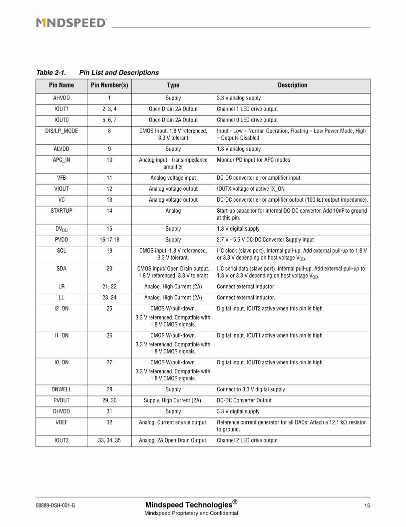
Table 2-1. Pin List and Descriptions
Pin Name Pin Number(s) Type Description
AHVDD 1 Supply 3.3 V analog supply
IOUT1 2, 3, 4 Open Drain 2A Output Channel 1 LED drive output
IOUT0 5, 6, 7 Open Drain 2A Output Channel 0 LED drive output
DIS/LP_MODE 8 CMOS Input. 1.8 V referenced, 3.3 V tolerant
Input - Low = Normal Operation, Floating = Low Power Mode, High = Outputs Disabled
ALVDD 9 Supply 1.8 V analog supply
APC_IN 10 Analog input - transimpedance amplifier
Monitor PD input for APC modes
VFB 11 Analog voltage input DC-DC converter error amplifier input
VIOUT 12 Analog voltage output IOUTX voltage of active IX_ON
VC 13 Analog voltage output DC-DC converter error amplifier output (100 kΩ output impedance).
STARTUP 14 Analog Start-up capacitor for internal DC-DC converter. Add 10nF to ground at this pin.
DVDD 15 Supply 1.8 V digital supply
PVDD 16,17,18 Supply 2.7 V - 5.5 V DC-DC Converter Supply input
SCL 19 CMOS input. 1.8 V referenced. 3.3 V tolerant.
I2C clock (slave port), internal pull-up. Add external pull-up to 1.8 V or 3.3 V depending on host voltage VDD.
SDA 20 CMOS input/ Open Drain output. 1.8 V referenced. 3.3 V tolerant
I2C serial data (slave port), internal pull-up. Add external pull-up to 1.8 V or 3.3 V depending on host voltage VDD.
LR 21, 22 Analog. High Current (2A) Connect external inductor
LL 23, 24 Analog. High Current (2A) Connect external inductor.
I2_ON 25 CMOS W/pull-down.
3.3 V referenced. Compatible with 1.8 V CMOS signals.
Digital input. IOUT2 active when this pin is high.
I1_ON 26 CMOS W/pull-down.
3.3 V referenced. Compatible with 1.8 V CMOS signals.
Digital input. IOUT1 active when this pin is high.
I0_ON 27 CMOS W/pull-down.
3.3 V referenced. Compatible with 1.8 V CMOS signals.
Digital input. IOUT0 active when this pin is high.
DNWELL 28 Supply Connect to 3.3 V digital supply
PVOUT 29, 30 Supply. High Current (2A). DC-DC Converter Output
DHVDD 31 Supply 3.3 V digital supply
VREF 32 Analog. Current source output. Reference current generator for all DACs. Attach a 12.1 kΩ resistor to ground.
IOUT2 33, 34, 35 Analog. 2A Open Drain Output. Channel 2 LED drive output
08889-DSH-001-G Mindspeed Technologies®15
Mindspeed Proprietary and Confidential
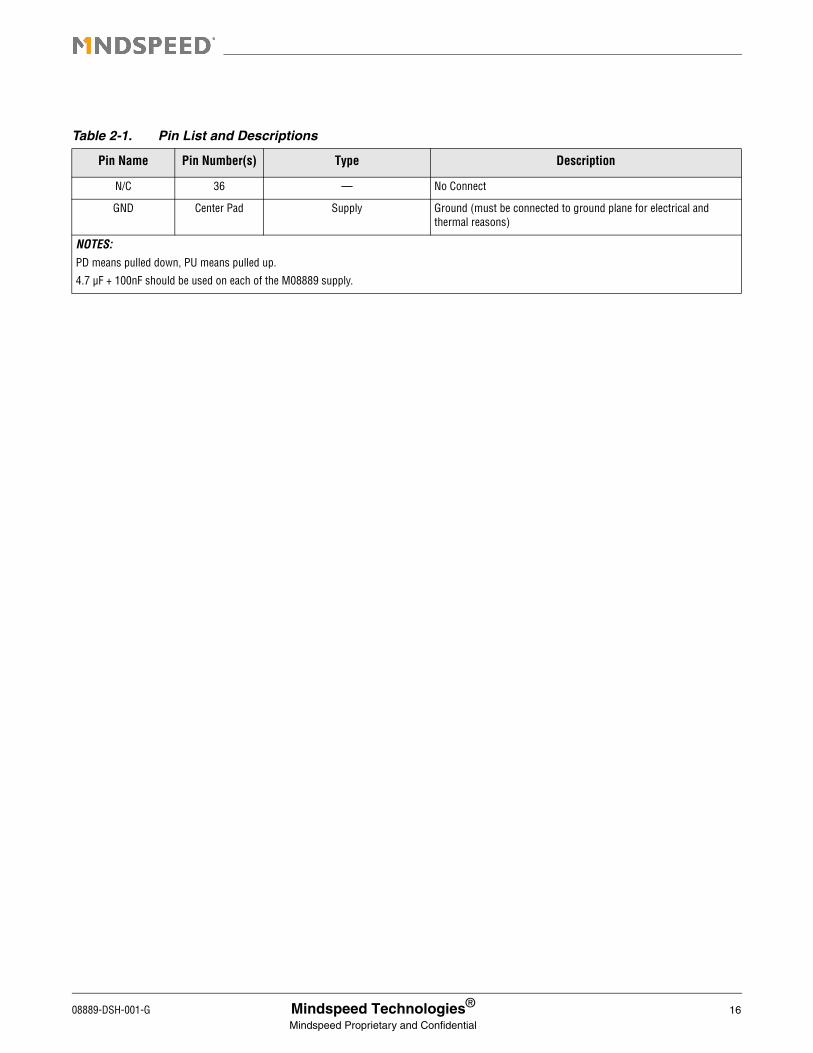
N/C 36 — No Connect
GND Center Pad Supply Ground (must be connected to ground plane for electrical and thermal reasons)
NOTES:PD means pulled down, PU means pulled up.
4.7 µF + 100nF should be used on each of the M08889 supply.
Table 2-1. Pin List and Descriptions
Pin Name Pin Number(s) Type Description
08889-DSH-001-G Mindspeed Technologies®16
Mindspeed Proprietary and Confidential

2.2 Package Information
Figure 2-2. Sawn QFN32 Package Information
08889-DSH-001-G Mindspeed Technologies®17
Mindspeed Proprietary and Confidential

08889-DSH-001-G
3.0 Functional Description
The M08889 is a highly integrated LED/laser driver with synchronous buck-boost converter for LCD/LCoS/DLP projection display applications. It provides control and monitoring of up to three LEDs/lasers, a temperature sensor and control of external DC-DC converters for optimal laser/led supply voltage.
Each Laser/LED output consists of a 10-bit DAC which controls a high efficiency driver. If the desired maximum current is less than 2 A the output resolution can by improved by a 6-bit independent scaling DAC.
The output stages require only 200 mV of headroom between the M08889 output and the Laser/LED cathode when driving 2 amperes. The headroom requirement can be scaled proportionally lower for lower currents.
The M08889 also incorporates safety and alarm features and a temperature monitor with 8-bit resolution.
The M08889 internal registers are loaded from an external micro controller through a slave I2C interface. The host micro controller can monitor the temperature sensor and read back the analog to digital converter outputs on the I2C interface.
3.1 Operating ModesThe M08889 can operate in 3 different optical power control modes. The power control modes are open loop (OL) and 2 automatic power control (APC) modes: continuous power control (CPC) and integrating power control (IPC).
Different output channels can have different operating modes. Some channels may be configured as Open Loop and some channels may be configured to use APC, but only one type of APC may be used (either CPC or IPC).
Open Loop mode is the simplest mode of operation and the Laser/LED current is set by writing the desired current to the output DAC.
The 2 automatic power control modes (APC) use photodiode feedback to accurately adjust the Laser/LED output power to make the current from a photodiode match a target current. With APC control temperature compensation of the Laser/LED is automatic and color balance is simplified.
The user can select the polarity of the photodetector if an APC mode is selected. By default the M08889 accepts a current source photodetector tied to the positive supply. It is possible to accept current sink photodetector by setting register.ipc_setup.bit[4]=1b.
Configuration of the M08889 timer settings and pin 8 configuration will also affect optical power control.
3.1.1 Open Loop Output ControlIn open loop mode the current for each Laser/LED is stored in register.ioutx[9:0]. The M08889 will shift the contents of register.ioutx[9:0] and register.ioutx_scale[5:0] to the output DAC when pin.Ix_ON goes high and the output will then sink the programmed current through the Laser/LED.
By changing the scale setting in register.ioutx_scale the full 10 bits of settability can be retained even for low Laser/LED currents. The scale can be changed on a frame by frame basis but when register.ioutx_scale is changed the rise time of the output stage will be significantly slower during the first Ix_ON period in which the
Mindspeed Technologies®18
Mindspeed Proprietary and Confidential

change in the scale is made. The rise time will return to its normal value in subsequent Ix_ON periods if the scale is not changed.
The M08889 includes timers that can be used to delay, pulse width modulate or clock the Open Loop output signal. See Section 3.6 for a description of how to use these features.
When pin 8 operates in LP_MODE (pin 8 floating) the scale value of each channel can be different than when pin 8 is in normal mode (pin 8 low). These scales are set in register.ioutx_scale[5:0] (pin 8 low) and register.ioutx_scale_LP[5:0] (pin 8 floating).
Table 3-1. Register Set-up for Open Loop Operation
Name Address RecommendSetting Description
opmode_ctrl0 0x00 50h Enable self-calibration of pin.IOUTx headroom.
opmode_ctrl1 0x01 80h or 90h Recommended setting.
reserved 0x03 80h Disable DC-DC speed-up circuit.
out_ctrlx 0x05, 0x06, 0x07 7Fh Recommended DC-DC feedback setting.
tempsens_ctrl 0x08 22h Recommended temperature sensor configuration.
ioutx_msb 0x10[1:0], 0x14[1:0], 0x18[1:0]
xxb Two most significant bits of output current setting.
ioutx_lsb 0x11, 0x15, 0x19 xxh Eight least significant bits of output current setting.
ioutx_scale 0x12, 0x16, 0x1A 00xxxxxb Set the scaling of the output currents.
DC-DC_overvoltage 0x1F A0h Set DC-DC overvoltage protection to 5 V nominal.
DC-DC_mode 0x20 03h Recommended DC-DC converter configuration.
reserved 0x22 40 Recommended DC-DC converter configuration.
regref_setup 0x24 20h Recommended DC-DC converter feedback configuration.
regrefx_ctrl1 0x27, 0x2B, 0x2F 3Fh57h7FhAFh
Output headroom and decimation factor for pin.IOUTx current less than 0.6 A.
Output headroom and decimation factor for pin.IOUTx current from 0.6 A to 1 A.
Output headroom and decimation factor for pin.IOUTx current from 1 A to 1.5 A.
Output headroom and decimation factor for pin.IOUTx current from 1.5 A to 2.0 A.
regrefx_ctrl0 0x28, 0x2C, 0x30 44h Recommended DC-DC converter configuration.
DCDC_ctrl3 0x61 15h, then write 95h to this
register after 01h is written to 0x72.
Recommended DC-DC negative current limit (set to 7 A).
DCDC_ctrl2 0x62 2Fh Enable overvoltage protection and set positive current limit (set to 7 A).
DCDC_ctrl1 0x63 8Fh Enable internal DC-DC feedback.
DCDC_ctrl0 0x64 5Fh Recommended DC-DC converter configuration.
start_op 0x72 01h Register loading complete, begin operation.
08889-DSH-001-G Mindspeed Technologies®19
Mindspeed Proprietary and Confidential

3.1.2 Automatic Power ControlAutomatic power control (APC) can keep the laser/LED power constant and the color balanced by comparing the photodetector (RGB color sensor) currents to target values programmed into the 13-bit target DACs.
At power-up the APC can be enabled independently for each channel by setting register.apc_ctrl[x]. For channels with disabled APC the laser/LED currents are controlled through the serial interface using register.ioutx.bits[11:0].
The photodiode (RGB sensor) target values are programmed via the serial interface in registers target2[12:0], target1[12:0] and target0[12:0] respectively for pins IOUT2, IOUT1 and IOUT0. When the corresponding color is turned on as signaled by the transition of pins I0_ON, I1_ON or I2_ON from low to high the LED/Laser drive currents are automatically adjusted up or down to always make the photodetector current (RGB sensor current) match the target current.
If desired, these target currents can be adjusted on a frame by frame basis to optimize contrast and save battery power depending on the brightness required for a particular frame.
The target values are stored in registers target2[12:0], target1[12:0] and target0[12:0] respectively for pins IOUT2, IOUT1 and IOUT0 before the corresponding color is turned on by the transition of pins I2_ON, I1_ON or I0_ON from low to high. This allows for the control of the LED/laser power in real time on a frame by frame basis.
It is possible to freeze the APC loop for each channel by using register.apcx_ctrl0[0]. In this case the M08889 will stop updating the pin.IOUTx currents.
If more then one laser is turned on (2 or 3 of I0_ON, I1_ON or I2_ON are high at the same time) the M08889 freezes the update of the APC loop for as long as more then one of the pin.Ix_ON signals are high. This prevents the APC loop from using incorrect photodetector information in case a single photodetector is used. In the case of multiple pin.Ix_ON simultaneously the optical power tracked and adjusted is that of the channel corresponding to the last pin.Ix_ON transitioning high. It should be noted that 2 or more low to high transitions of any of the pins I0_ON, I1_ON or I2_ON within 500 ns of each other would violate internal timing and will result in unpredictable operation. Care should be taken to prevent damage to the part when multiple lasers are enabled. The power dissipation of the M08889 should be kept below the level that, when multiplied by the thermal resistance of the package in the system and added to the maximum ambient temperature, does not exceed 125 °C.
The maximum photodiode current supported by the M08889 is 3.25 mA. The full scale value of the target DAC is 3.25 mA with a resolution of 13 bits (390 nA step size). As an example, if the maximum current from the photodiode is 200 µA then the possible target values are up to 512 decimal (200 µA/390 nA). In this example the maximum target value for register.targetx[12:0] would be 200 h.
Read-back of the output current DAC of each channel is possible by strobing the DACs using register.strbalarm_ctrl[1] and reading registers.rb_ioutx[9:0]
When pin 8 is floating the M08889 will be in Low Power mode (LP_MODE). When pin 8 is low the Laser/LED current will be adjusted until the photodiode current matches the target in register.targetx[12:0] and when pin 8 is floating the Laser/LED current will be adjusted until the photodiode current matches the target in register.targetx_LP[12:0].
The M08889 is capable of using current sink photodetectors typical of LCOS panels as well as photodetectors that source current. The type of photodetector can be selected at register.ipc_setup[4].
The photodetector can have a maximum capacitance of up to 300 pF.
3.1.2.1 Continuous Power ControlIn continuous power control (CPC) mode, the M08889 continuously compares the photodetector current to a target value and makes photodiode current match the target value by adjusting the current in the laser/LED. For example, if the photodetector current is below the target then the Laser/LED current is increased. The sign of this operation
08889-DSH-001-G Mindspeed Technologies®20
Mindspeed Proprietary and Confidential

can be inverted using register.input_ctrl[4] (but it should not be changed unless it is certain that there is an inversion in the photodiode signal).
The CPC loop is designed to settle to the desired output power in less than 50 µs. To achieve optimal settling time, the CPC loop must be adjusted to the laser/photodetector characteristics. This is done using the settings in registers apcx_ctrl0, apcx_ctrl1 and apcx_ctrl2.
To further reduce the settling time the user can program the initial current from which the CPC loop will start. This can be 0, the value programmed in register.ioutx[9:0] or the value to which the CPC had converged during the previous frame. The selection of the initial current is done using register.iturnonx[1:0] (apcx_ctrl1[3:2]). Starting from the previously determined value will substantially accelerate settling time since it is likely that it will be starting at the proper level.
It is possible to “freeze” the APC loop for each channel by using register.apc_ctrl[x]. When register.apc_ctrl[x]=1b the M08889 will stop updating the pin.IOUTx currents regardless of the state of Ix_ON pins. It is possible also to delay operation of the CPC loop immediately following the light source turn-on. This will allow the DC-DC converter to settle to the proper voltage before the APC starts adjusting the current. The CPC delay time can be programmed using register.apcx_ctrl0[2:1].
3.1.2.2 Integral Power ControlIntegral power control (IPC) can be enabled by setting register.apc_ctrl[6]=0b.
The working principle of integral power control is to use pulse-width modulation to mimic the behavior of the human eye which integrates the optical power over the frame period. The Ix_ON time is determined in the M08889 by charging a capacitor with the photodetector current until the capacitor reaches a threshold voltage at which time the output turns off.
When pin.Ix_ON goes high the M08889 will drive the Laser/LED with a current defined by register.ioutx[9:0]. The photodiode current will charge an internal capacitor until its voltage matches an internal reference voltage (~0.8 V)
Table 3-2. Additional Registers used for CPC Control (Table 3-1 settings are also needed)
Name Address RecommendSetting Description
apc_fe_ctrl 0x0A 01h Power-on APC photodiode circuitry.
loop select
apc0_ch
apc1_ch
apc2_ch
0x34[6]
0x34[0]
0x34[1]
0x34[2]
1b
xb
Select CPC loop control.
Enable CPC control on the desired channel or channels.
targetx_msb
targetx_lsb
0x35, 0x37, 0x39
0x36, 0x38, 0x3A
000xxxxxb
xxh
Set the target at desired level. The LED drive current will be adjusted up or down until the photodiode current is equal to the target current for the channels that are controlled by CPC.
apc0_ctrl2
apc1_ctrl2
apc2_ctrl2
0x47
0x44
0x41
xxh Set the length in clock counts of the initial, mid and min step intervals. Set the delay for the clock divider. The decimation factor and clock divider will also affect interval lengths.
apc0_ctrl1
apc1_ctrl1
apc2_ctrl1
0x48
0x45
0x42
xxh Set the step size of the change in LED drive current for the initial and mid intervals. Set the initial LED current to be 0 mA, the ending value of the previous I_on period or the value set in IOUTx register. Set the clock divider.
apc0_ctrl0
apc1_ctrl0
apc2_ctrl0
0x49
0x46
0x43
xxx00xx0b Set the decimation factor (mid and min count changes will occur at rate divided by the decimation factor). Set the WAIT states (APC will not change LED current during WAIT states).
08889-DSH-001-G Mindspeed Technologies®21
Mindspeed Proprietary and Confidential
at which time a counter is incremented and the capacitor is discharged. The photodiode current continues to charge the capacitor and increment the counter until the count matches the target set by the user in register.targetx[9:0]. Once the counter reaches the value set by the user the M08889 stops driving the Laser/LED. By adjusting the count higher or lower the brightness of a frame can be adjusted. The target counter has 10 bits and the M08889 can distinguish between 1024 different power levels. The target registers are the same as the CPC target registers but the resolution in IPC mode is limited to 10 bits instead of 13 bits.
In order to maximize the dynamic range and be able to utilize the entire 10 bits the user must select the proper mirroring ratios for the photodetector current (register.ipdx_sel[4:0]), the charging current (register.ichx_sel[4:0]) and the value of the capacitance (register.capx_sel[3:0]). The settings of these bits will depend on the frame (or subframe) duration and on the photodetector current.
If it is desired to typically have the LED on for 1/2 the frame time then the registers should be configured such that:
1/2 x FR/512 = 0.8 V x Cch / Ich
where FR is the frame or subframe rate, Cch is the charging capacitors selected through register.capx_sel[3:0], and Ich is the resulting charging current obtained by multiplying the photodetector current by register.ipdx_sel[4:0] and by register.ichx_sel[4:0] mirroring ratios. The factor of 512 is length of the 10 bit range.
Cch = 25 pF + N x 2.5 pF where N is the setting of register.capx_sel[3:0].
Ich = (Iphotodetector / register.ipdx_sel[4:0]) x register.ichx_sel[4:0] where Iphotodetector is the photodiode current
As in CPC mode, when pin 8 operates in LP_MODE (pin 8 floating) the target power value can be changed. When pin 8 is low the Laser/LED current will be on until the photodiode count matches the target in register.targetx[9:0] and when pin 8 is floating the Laser/LED current will be on until the photodiode count matches register.targetx _LP[9:0].
The photodiode input can be changed from sinking to sourcing at register.ipc_setup[4] and an additional scaling factor of 0.4 is available at register.ipc_setup[5].
Example: Assume that the photodiode current is 150 µA when the LED is on at the desired amplitude, the pin.Ix_ON time is 1 ms and it is desired that the LED be on approximately 50% of this time. The mirroring ratio should be set to the 200 µA range (register.ichx_sel[4:0] = 00001b), choose a Cch = 25 pF with register.ichx_sel[4:0] = 00000b (any other value is also OK but using the default value means this register never needs to be written), choose a mirroring ratio such that the Cch can be charged to 0.8 V several hundred times in 0.5 ms. If it is desired that it be charged ~250 times in 0.5 ms then:
0.5 ms/250 =0.8 V x 25 pF /((150 µA / 200 µA) x register.ichx_sel[4:0]) 0.002 ms = 26.67e-12 / register.ichx_sel[4:0] register.ichx_sel[4:0] = 2.667e-5 / 2 which is between 10 µA and 20 µA so set register.ichx_sel[4:0] =00001b
08889-DSH-001-G Mindspeed Technologies®22
Mindspeed Proprietary and Confidential
3.2 Color MixingThe M08889 supports color mixing but with some limitations. The M08889 will not automatically determine which LED or laser has the largest voltage drop and automatically adjust the DC-DC converter voltage to this voltage. The M08889 DC-DC will always optimize the DC-DC converter output voltage to the pin.IOUTx corresponding to the active pin.Ix_ON. The Mindspeed M08890 and M08898 have the capability to optimize the external DC-DC output voltage to the LED/Laser with the largest forward voltage regardless of whether it corresponds to the active pin.Ix_ON.
If color mixing is used with the M08889 then small resistances should be added in series with the LEDs/Lasers to guarantee that the forward voltage of the LED/Laser is greatest for the active pin.Ix_ON.
The color mixing registers are 0x65 through 0x71. The M08889 cannot work in the IPC or CPC modes with color mixing, the operating mode must be Open Loop (no photodiode or color sensor).
It is also important to make sure that the sum of the IOUTx currents never exceeds 2 A or the M08889 may be damaged.
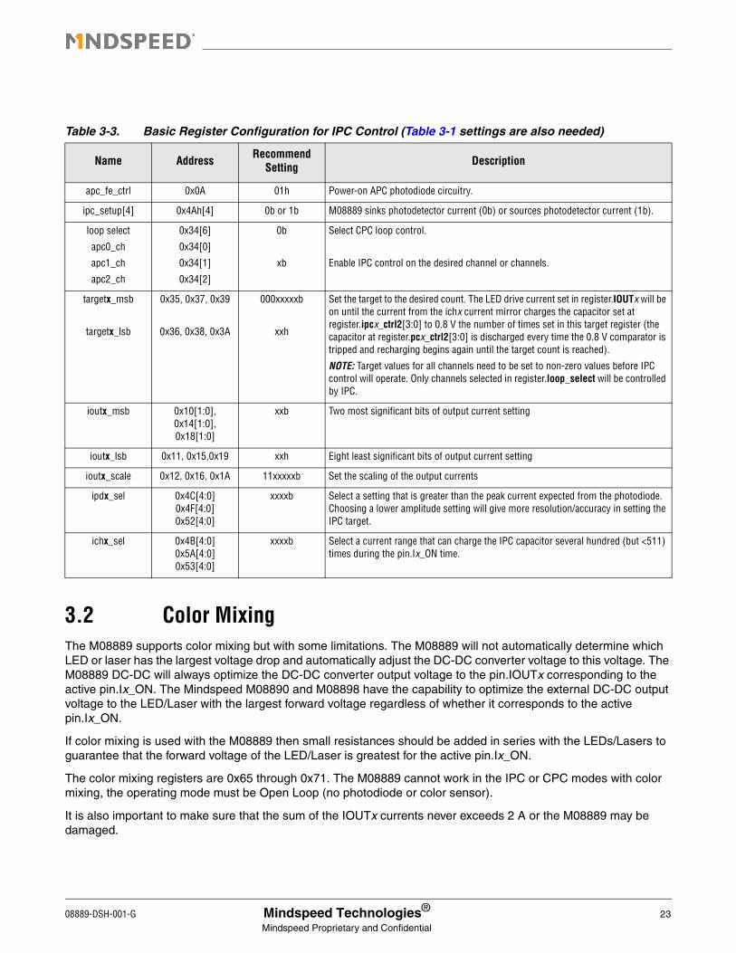
Table 3-3. Basic Register Configuration for IPC Control (Table 3-1 settings are also needed)
Name Address RecommendSetting Description
apc_fe_ctrl 0x0A 01h Power-on APC photodiode circuitry.
ipc_setup[4] 0x4Ah[4] 0b or 1b M08889 sinks photodetector current (0b) or sources photodetector current (1b).
loop select
apc0_ch
apc1_ch
apc2_ch
0x34[6]
0x34[0]
0x34[1]
0x34[2]
0b
xb
Select CPC loop control.
Enable IPC control on the desired channel or channels.
targetx_msb
targetx_lsb
0x35, 0x37, 0x39
0x36, 0x38, 0x3A
000xxxxxb
xxh
Set the target to the desired count. The LED drive current set in register.IOUTx will be on until the current from the ichx current mirror charges the capacitor set at register.ipcx_ctrl2[3:0] to 0.8 V the number of times set in this target register (the capacitor at register.pcx_ctrl2[3:0] is discharged every time the 0.8 V comparator is tripped and recharging begins again until the target count is reached).
NOTE: Target values for all channels need to be set to non-zero values before IPC control will operate. Only channels selected in register.loop_select will be controlled by IPC.
ioutx_msb 0x10[1:0], 0x14[1:0], 0x18[1:0]
xxb Two most significant bits of output current setting
ioutx_lsb 0x11, 0x15,0x19 xxh Eight least significant bits of output current setting
ioutx_scale 0x12, 0x16, 0x1A 11xxxxxb Set the scaling of the output currents
ipdx_sel 0x4C[4:0]0x4F[4:0]0x52[4:0]
xxxxb Select a setting that is greater than the peak current expected from the photodiode. Choosing a lower amplitude setting will give more resolution/accuracy in setting the IPC target.
ichx_sel 0x4B[4:0]0x5A[4:0]0x53[4:0]
xxxxb Select a current range that can charge the IPC capacitor several hundred (but <511) times during the pin.Ix_ON time.
08889-DSH-001-G Mindspeed Technologies®23
Mindspeed Proprietary and Confidential

3.3 Digital CMOS InputsPin.Ix_ON inputs will control which of the pin.IOUTx outputs are sinking current. When address 02h[7]=0b then pin.IOUT0 will be active when pin.I0_ON is high and pin.IOUT1 will be active when pin.I1_ON is high and pin.IOUT2 will be active when pin.I2_ON is high. Multiple pin.Ix_ON inputs may be active (high) at the same time but the sum of the pin.IOUTx currents should not exceed 2 A or the DC-DC output current limit will be exceeded and the package power dissipation limit may be exceeded.
The pin.Ix_ON inputs are 3.3 V and 1.8 V CMOS compatible provided that the 1.8 V signal VOH is > 0.65
Pin.DIS/LP_MODE input has 1.8 V CMOS tri-state levels and is 3.3 V tolerant. When this input is left floating an internal resistive divider will pull this input to ~3.3 V/2. The input impedance of the divider is ~100 kΩ.
3.3.1 Using only pin.I0_ON and pin.I1_ON to Control All Three OutputsWhen address 02h[7]=1b pin.I0_ON and pin.I1_ON inputs are multiplexed to control all three outputs and pin.I2_ON is ignored. The table below shows the coding for these 2 inputs and the 3 outputs.
Table 3-4. Additional Registers used for Color Mixing (Table 3-1 settings are also needed)
Name Address RecommendSetting Description
cm_setup 0x65 3Fh All 3 channels on simultaneously. Set color mixing currents such that DC-DC converter output current does not exceed 2 A.
ioutx_cmy_msb 0x66[1:0]0x68[1:0]0x6A[1:0]0x6C[1:0]0x68F1:0]0x70[1:0]
xxb Two most significant bits of output current setting for pin.IOUTx when IOUTy is the active channel.
ioutx_cmy_lsb 0x670x690x6B0x6D0x690x71
xxh Eight least significant bits of output current setting for pin.IOUTx when IOUTy is the active channel.
Table 3-5. Using I0_ON and I1_ON inputs to Control all 3 Outputs
I0_ONstate
I1_ONstate
IOUT0state
IOUT1state
IOUT2state
low low OFF OFF OFF
low high OFF OFF ON
high low OFF ON OFF
high high ON OFF OFF
08889-DSH-001-G Mindspeed Technologies®24
Mindspeed Proprietary and Confidential

3.4 Outputs
3.4.1 LASER/LED Current DACsThe M08889 includes three monotonic DACs which generate the currents for the three LED output drivers.
The three DACs have a maximum range from 0 to 2 A, a resolution of 10 bits and a maximum update rate of 12.5 Msps. The output rise time will be limited by the M08889 output current driver unless a single DC-DC converter is used for more than one Laser/LED, in which case the DC-DC converter settling time and overall supply loop behavior may determine the output rise time.
The full scale of each output DAC can be programmed through register.ioutx_scale.bits[5:0] independently for each channel. The scale DAC changes the full scale of each output current DAC from a minimum of 200 mA to a maximum of 2 A in steps of 28.57 mA. At power-up the scale DACs are set at maximum scale (2 A).
3.4.2 Output Current DriversThe integrated output current drivers deliver the DAC currents to the Lasers/LEDs.
Each Laser/LED driver output (IOUTx) is controlled by the corresponding ON signal (Ix_ON) and the PWM and MPG setting as described later. Rise/fall time of the driver is typically 200 ns into a resistive electrical load connected to a stable supply voltage. If a DC-DC converter is employed the response time of the current output may also depend on the response time of the DC-DC converter and the series resistance of the light sources. The rise and fall time is specified for any transition of the register.ioutx[9:0] for a constant register.ioutx_scale[5:0] code.
The drivers require a worst case headroom of 200 mV. The headroom is proportionally lower at lower drive currents. This value is programmed at register.regrefx_ctrl1.
The M08889 typical driver headroom follows the following equation:
VLDD = 100 mΩ x IOUT, but the headroom should always be set to at least 70 mV
The voltage at the laser driver output should never exceed 5.5 V. An external resistor should be used between the laser/LED cathode and ground to provide a small leakage current into the light source allowing the voltage at pin.IOUTx to be reduced from the anode voltage by the laser/LED voltage drop. The value of the resistor should be chosen such that the current flowing is enough to create a voltage drop on the laser while keeping the laser current far below threshold or, in the case of LEDs, low enough so as to not cause light pollution in the system.
3.4.3 Recommended Snubbing Network at IOUTx PinsA snubbing network of 1 µF in series with 1.5 Ω should be placed in parallel with the LED/Laser at each IOUTx pin. The inductance in series with the LED/Laser should be less than 500nH.
The routing of the snubbing network on the circuit board should be as short as possible between pin.IOUTx and the capacitors on pin.PVOUT. The resistor should be placed close to pin.IOUTx.
08889-DSH-001-G Mindspeed Technologies®25
Mindspeed Proprietary and Confidential

3.5 Controlling the Output Voltage to Optimize Power Consumption
The system power dissipation will be dominated by the Laser/LED current and the bias voltage of the Laser/LED. For each ampere of Laser/LED current, each 100 mV of excess Laser/LED bias voltage results in 100 mW of wasted power.
The M08889 minimizes the voltage drop on the output stage and optimizes overall power dissipation by adjusting the anode voltage of the light sources at the output of the DC-DC converter. Given the expected maximum current for a particular LED/laser on a channel, the user can program the headroom required for each channel based on the equations above (Section 3.4.2) to optimize system power. Whether or not a pin.IOUTx and LED is connected to the DC-DC converter output voltage the required headroom of the M08889 outputs must be maintained when the corresponding pin.Ix_ON is high (see Section 3.4.2).
If the input voltage at pin.PVDD falls below 2.45 V the DC-DC converter will be disabled until the voltage rises above 2.45 V to prevent damage to the DC-DC converter. Voltage spikes below 2.45 V at pin.PVDD should be avoided.
3.5.1 Control of M08889 Internal DC-DC ConverterTypical register settings to allow control of the internal DC-DC converter are shown below.
The M08889 DC-DC converter control circuitry uses a 9-bit DAC to set a feedback factor for the external DC-DC converter and adjust the anode voltage of the Laser/LEDs. The DAC is controlled by a digital filter with programmable update rate and decimation factor. The digital filter is fed by a comparator which increments or decrements the counter code depending on whether the headroom of the driver is higher or lower than the programmed headroom. The above operations are performed automatically by the M08889 and no interaction with the M08889 is required beyond initializing the register settings as described at the beginning of this section.
Once the LED is turned off the value of the DAC inputs are stored by the M08889. The next time this LED is active, the loop will automatically start from the stored DAC value. The initial value of the DAC code can be selected
Table 3-6. Basic Register Configuration for External DC-DC Control
Name Address Recommended Setting Description
opmode_ctrl0 0x00 50h Enable self-calibration of pin.IOUTx headroom.
regref_setup 0x24 20h Recommended DC-DC converter feedback configuration.
regrefx_ctrl1 0x27, 0x2B, 0x2F
67h7Fh97hAFh
Output headroom and decimation factor for 0.5 A. Output headroom and decimation factor for 1.0 A. Output headroom and decimation factor for 1.5 A. Output headroom and decimation factor for 2.0 A.
DC-DC_mode 0x20 03h Recommended DC-DC converter configuration.
regrefx_ctrl0 0x28, 0x2C, 0x30
44h Recommended DC-DC converter configuration.
DCDC_ctrl3 0x61 15h, then write 95h to this register after 01h is
written to 0x72.
Recommended DC-DC negative current limit (set to 7 A).
DCDC_ctrl2 0x62 2Fh Enable overvoltage protection and set positive current limit (set to 7 A).
DCDC_ctrl1 0x63 8Fh Enable internal DC-DC feedback.
DCDC_ctrl0 0x64 5Fh Recommended DC-DC converter configuration.
08889-DSH-001-G Mindspeed Technologies®26
Mindspeed Proprietary and Confidential

through register.regrefx_ctrl0[3:2] to be either the previously determined value, 0 or the value written in register.regrefx_dac.
The headroom, decimation filter and update rate can be programmed independently for each channel using register.regrefx_ctrl1[7:3], register.regrefx_ctrl1[2:0] and register.regrefx_ctrl0[7:5] respectively.
If more then one output is being turned on at the same time, the regref will control the DC-DC converter for the headroom of the last output turned on.
If CPC is used, the user should program the headroom for the highest expected output current.
The initial update of the IDAC which controls the LED/Laser supply headroom can be delayed through register.regrefx_ctrl0[1:0] to allow the DC-DC converter to settle before turning on the LED/Laser. This may be a useful setting when using CPC mode.
In the case of integrating power control mode the speed of the DC-DC converter settling is not important: the light source current will be equal to the programmed current if the headroom is higher or equal to the required and will be smaller if the headroom is less then the required headroom. However, this will not matter as long as the frame/subframe time is long enough to guarantee that the integrated power over the time meets the target.
The monotonic DAC used for controlling external DC-DC converters has a full scale current of 100 µA and 9 bits of resolution. The full scale can be increase by a factor of 2 to 200 µA by setting register.regref_setup[1]=1b.
3.6 TimersThe M08889 features internal timers which allow an extra layer of control of the current by means of pulse width modulation (PWM) and multi pulse generation (MPG)
The clock source for the internal timer circuitry can be either the internal 25 MHz oscillator or an external clock fed through CLK_IN (pin 8).
With reference to the following diagram for channel 0 (pin.I0_ON, pin.IOUT0), PWM controls the “On delay time” while MPG adjusts independently both the “Pulse on time” and “Pulse off time”.
3.6.1 Pulse Width Modulation (PWM) Activating pulse width modulation will allow the output current to be delayed with respect to the pin.Ix_ON signal. This may be useful if a blanking period is needed to allow the LCD or DLP to settle or it may be useful to save power if a laser is used and the same optical output can be achieved with fewer coulombs if higher laser driver currents and shorter durations are used (the coulombs will be less with higher current and shorter duration if the
Figure 3-1. Example of PWM and MPG Timers
Color fram e/subfram e tim e
O n delay tim e Pulse on tim ePulse off tim e
I0_ON
IOUT0
M ulti pulse genration (M PG)Pulse w idth m odulation
(PW M)
08889-DSH-001-G Mindspeed Technologies®27
Mindspeed Proprietary and Confidential

laser threshold current is approximately the same with PWM activated at higher current as it is at lower current without PWM activated).
PWM works in all optical power control modes: Open Loop, CPC and IPC.
The PWM delay is implemented with a 10-bit counter that counts the clock cycles of an internal 25 MHz oscillator. At the rising edge of each pin.Ix_ON the counter is decremented and the Laser/LED is turned on when the counter reaches 0. The laser is turned off as usual on the falling edge of the corresponding pin.Ix_ON signal. The maximum delay achievable is ~41 µs (1023 times the 40 ns period of the internal oscillator). Additional delay can be achieved by using the M08889 programmable divider of the internal clock. The internal clock can be divided down by a factor of 1, 2, 4, 8, 16, 32, 64, and 128. This can be obtained by writing register.clk_div_pwm[3:0]. The maximum delay is therefore equal to ~5.24msec.
The values of the programmable counter are stored in register.on_countx[9:0]. The rising edge of the pin.Ix_ON signal strobes the corresponding register.on_countx[9:0] value into the M08889 in the same fashion as other output current settings such as register.targetx[12:0] and register.ioutx[9:0]. If the on_count register value is changed during the on time for that color the effect of the register change will be available during the next pin.Ix_ON cycle.
If register.on_countx is programmed to 000h the PWM feature is disabled for pin.IOUTx.
The internal ring oscillator clock will vary by as much as ±15% over process, temperature and supply. If this accuracy is not acceptable then pin 8 can be defined to be a clock input and a more accurate external clock signal can be used. The PWM block is designed to operate with a maximum frequency of 25 MHz. The PWM generator will work at the speed of the signal at CLK_IN (pin 8) when the external clock is selected with register.clk_ctrl[2].
3.6.2 Multi Pulse Generator (MPG)
A less than 100% duty cycle pulsed waveform can be programmed into the M08889 using the Multi-Pulse Generator (MPG).
The multi-pulse generator (MPG) operates in a similar manner of the PWM generator. For each of the Lasers/LED outputs, two 10-bit counters specify the number of 25 MHz internal clock cycles during which the output is on and off. As with the PWM timer, the MPG timer can be controlled by an external clock signal at CLK_IN (pin 8).
The duty cycle of the pulsed waveform is resolved in 25 MHz clock periods or 40 ns steps. If both counters are loaded with the maximum value (1023) the waveform driving the output will be a clock of period ~81 µs.
The clock can be divided down to lower rates by programming register.clk_div_mpg[3:0].
Figure 3-2. Multi Pulse Generator Timing
30% frame time
On delay time Pulse on timePulse off time
I0_ON
IOUT0
08889-DSH-001-G Mindspeed Technologies®28
Mindspeed Proprietary and Confidential

MPG works in all optical power control modes: Open Loop, CPC and IPC. However if IPC or CPC power control is employed, the minimum divider ratio at register.clk_div_mpg[3:0] is 8. Care should be taken when MPG is used while controlling the DC-DC converter as the slow response time of the DC-DC converter to variation in the light source drop may create oscillation and instability. It is recommended that register.opmode_ctrl0[5]=1 if analog control mode is used to control the DC-DC converter. In this setting the DC-DC converter feedback will not be driven while the LED current is off (pulse off time). To prevent the DC-DC converter from drifting away from the optimal headroom operating point external resistive feedback R1/R2 should be added as shown in Figure 1-2. The effective resistance of R1/R2 should be 500 kΩ.
Because a 10-bit counter is used, the duty cycle resolution obtainable is 1/1023 or better then 0.1% assuming the highest count value is used for one of the counters. The duty cycle accuracy is inversely proportional to the maximum counter value.
The control for pin.IOUTx output on pulse is programmed in register.pulse_onx[9:0]. The off pulse is programmed in register.pulse_offx[9:0].
The rising edge of the pin.Ix_ON signals strobe the corresponding pin.pulse_on/offx[9:0] values into the M08889 timing controller. If the pulse_on/pulse_off register values are changed during the on time for that output the MPG setting will not be changed until the next pin.Ix_ON cycle.
If either the pulse_on or pulse_off for a channel is programmed to 000h then the MPG function is disabled for that channel.
3.7 Temperature SensorThe M08889 features an internal temperature sensor which measures the internal junction temperature of the part. The information is converted by the ADC and can be read through the serial interface at register.temp[7:0].
The ambient temperature of the system can be calculated from the part junction temperature, the part power dissipation and the package thermal resistance (temperature measurements can vary dramatically at different locations within a system and measurements are dependent on mechanical factors such as PCB area, material and number of layers, airflow, heatsinking, etc.)
Absolute accuracy of the temperature sensor is ±10 °C after calibration at room temperature. Its resolution is 8-bit or 0.65 °C over the range of -40 °C to 125 °C.
3.8 SafetyUsing this driver for LEDs or Lasers in the manner described in this data sheet does not ensure that the resulting optical emissions comply with established standards such as IEC825. Designers must take the necessary precautions to ensure that eye safety and other applicable standards are met. Note that determining and implementing the level of fault tolerance required by the applications that this part is going into is the responsibility of the projector designer and manufacturer since the application of this device cannot be controlled by Mindspeed.
A disable pin (DIS) is available in the M08889. It disconnects the path to ground or supply: within 1 µs of a low to high transition of pin.DIS, the laser driver current is reduced to 1/10th of its starting value. Moreover the part is put in a low power dissipation mode.
A register alarm is available: the safety block compares the output current of each Laser/LED with 3 thresholds (one for each of the lasers/LEDs) and an alarm is issued if the current is higher then the programmed thresholds. The digital thresholds can be programmed in registers.alarm_thx[7:0], these represent the MSB of the output current.
08889-DSH-001-G Mindspeed Technologies®29
Mindspeed Proprietary and Confidential

It should be noticed that register.alarm[7:0] is not self clearing: once an alarm has occurred, it must be cleared by the user by writing 1 to clear_alarm (register.alarm_ctrl[0]).
The M08889 can also be programmed (register.opmode_ctrl1[3]) for automatic shutdown if the programmed threshold is exceeded. In this case the output current for that output is automatically forced to 0 by forcing 0 to the DAC inputs. This feature can be disabled via registers.
The output stage can also be disabled by the user via register, through register.opmode_ctrl1.bits[1:0].
3.9 AlarmThe M08889 is capable of detecting an open or a short at the driver outputs and it will issue an alarm if a voltage lower then the programmed threshold is detected at pin.IOUTx outputs while the Laser/LED is not driven. Similarly, while the Laser/LED is driven, an alarm is issued if the voltage at pin.IOUTx decreases below a preprogrammed threshold. This would indicate an open LED as the driver will force the pin.IOUTx voltage to 0 if no LED is connected.
The LED alarms can be enabled and programmed independently for each channel using register.alarm_setup0[7:0] and register.alarm_setup1[3:0].
The alarm status can be read back at register.alarm_iout[2:0]. This register is not self clearing.
To prevent false alarms caused by slow DC-DC converter settling the alarm signal can be delayed using register.alarm_set1[5:4].
3.10 Power Supply SequencingThe preferred M08889 power supply pin power-up and power-down sequencing is described in the diagrams below. The M08889 is designed to operate with arbitrary ordering of power supply pin power-up and power-down.
Figure 3-3. Power-Up
Figure 3-4. Power-Down
PVDD
DVDD, ALVDD, AHVDD>10μsec
PVDD
>1μsecDVDD, ALVDD, AHVDD
0V
0V
08889-DSH-001-G Mindspeed Technologies®30
Mindspeed Proprietary and Confidential

08889-DSH-001-G
4.0 Registers
Addresses 00h-0Dh: General registers for operating mode set-up.
Addresses 10h-1Eh: Output current registers to set the output current at pins IOUTx. These registers may be written at any time but their values will not become active until a rising edge at pin Ix_ON.
Addresses 1Fh-33h: DC-DC converter control registers.
Addresses 34h-40h: APC set-up registers. The APC target registers may be written at any time but their values will not become active until a rising edge at pin Ix_ON.
Addresses 41h-49h: CPC set-up registers.
Addresses 4Ah-53h: IPC set-up registers.
Addresses 54h-60h: Timer set-up for PWM and MPG. The Timer registers may be written at any time but their values will not become active until a rising edge at pin Ix_ON.
Addresses 61h-64h: DC-DC converter protection registers.
Addresses 65h-71h: Color Mixing registers. The Color Mixing registers may be written at any time but their values will not become active until a rising edge at pin Ix_ON.
Addresses 72h-74h: Initialization registers.
Addresses 75h-83h: Readback registers for monitoring M08889 operating state. Read only.
Addresses 86h: Strobe and clear alarm bit.
Table 4-1. Register Types
Name Description
R Read Only
R/W Read or Write.
R/Wa Read or Write. New value will not be active until next Ix_ON rising edge.
R/Wsc Read or Write. Self Clearing.
Mindspeed Technologies®31
Mindspeed Proprietary and Confidential
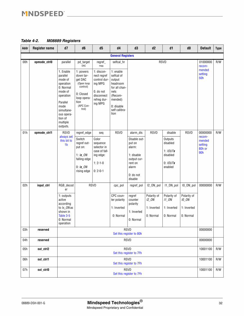
Table 4-2. M08889 Registers
Addr Register name d7 d6 d5 d4 d3 d2 d1 d0 Default Type
General Registers
00h opmode_ctrl0 parallel pd_targetDAC
regref_mpg
selfcal_hr RSVD 01000000recom-mended setting 50h
R/W
1. Enable parallel mode ofoperation 0: Normal mode of operation
Parallel mode simultane-ous opera-tion of multiple outputs.
1: powers down tar-get DAC
(Open loop control)
0: Closed loop opera-tion
(APC Con-trol)
1: discon-nect regref control dur-ing MPG 0. do not disconnect refreg dur-ing MPG
1: enable selfcal of output headroom for all chan-nels(Recom-mended) 0: disable self calibra-tion
01h opmode_ctrl1 RSVD always set this bit to
1b
regref_edge seq RSVD alarm_dis RSVD disable RSVD 00000000 recom-mended setting 80h or 90h
R/W
Switch regref out-put on: 1: Ix_ON falling edge 0: Ix_ON rising edge
Color sequence selector in case of fall-ing edge: 1: 2-1-0 0: 2-0-1
Disable out-put on alarm: 1: disable output cur-rent on alarm 0: do not disable
Outputs disabled 1: IOUTx disabled 0: IOUTx enabled
02h input_ctrl RGB_decoder
RSVD cpc_pol regref_pol I2_ON_pol I1_ON_pol I0_ON_pol 00000000 R/W
1: outputs active according to Ix_ON as shown in Table 3-5 0: Normal operation
CPC coun-ter polarity 1: Inverted
0: Normal
regref counter polarity 1: Inverted 0: Normal
Polarity of I2_ON 1: Inverted 0: Normal
Polarity of I1_ON 1: Inverted 0: Normal
Polarity of I0_ON 1: Inverted 0: Normal
03h reserved RSVDSet this register to 80h
00000000
04h reserved RSVD 00000000
05h out_ctrl2 RSVDSet this register to 7Fh
10001100 R/W
06h out_ctrl1 RSVDSet this register to 7Fh
10001100 R/W
07h out_ctrl0 RSVDSet this register to 7Fh
10001100 R/W
08889-DSH-001-G Mindspeed Technologies®32
Mindspeed Proprietary and Confidential

08h tempsens_ctrl RSVD pd_temp temp_cal[3:0] temp_gain[1:0] 01100000 (set this
register to 22h)
R/W
1: Powers down temp sensor 0: Temp sensor enabled (recom-mended)
Temperature sensor offset calibration (set these bits to 010b)
Calibrate temp sensor gain (set these bits to
10b)
09h tia_ctrl cpd_comp cf_ctrl cz_ctrl rz_ctrl rf_ctrl 00100110 R/W
Cpd com-pensation
1: 16 pF 0: 9 pF
Controls value of TIA
Cf 1: 700fF 0: 500fF
Controls value of CZ: APC compensation control: 11: 14 pF 10: 10 pF 01: 8 pF 00: 4 pF
Controls value of Rz: APC compensation control:
1x: 2.5kOhms 01: 3.75kOhms
00: 5kOhms
Controls value of Rf: TIA gain control:11: 20kOhms
10/01: 40kOhms 00: 60kOhms
tia_ctrl_d
0Ah apc_fe_ctrl RSVD Cpd_comp[1:0] RSVD pd_fe 00000001 R/W
Photodiode compensa-tion for APC inputs
APC photo-diode
amplifier power down
1: power down (no photodiode feedback or color sen-sor)
0: normal operation (APC Con-trol)
0Bh RSVD RSVD 00000000 R/W
0Ch alarm_setup0 led_alrm_rc1
led_alarm_thres1 en_ledalarm1
led_alrm_rc0
led_alarm_thres0 en_ledalarm0
00010001 R/W
LED alarm time con-
stant 1: 5usec 0: 2usec
LED alarm threshold for channel 1
00: 200 mV 01: 150 mV 10: 100 mV 11: 50 mV
Power down LED alarm for channel 1
1: power down 0: enable
LED alarm time con-
stant
1: 5usec0: 2usec
LED alarm threshold for channel 0
00: 200 mV 01: 150 mV 10: 100 mV 11: 50 mV
Power down LED alarm for channel 0
1: power down 0: enable
Table 4-2. M08889 Registers
Addr Register name d7 d6 d5 d4 d3 d2 d1 d0 Default Type
08889-DSH-001-G Mindspeed Technologies®33
Mindspeed Proprietary and Confidential

0Dh alarm_setup1 RSVD turnon_alarm_delay led_alrm_rc2
led_alarm_thres2 en_ledalarm2
00110001 R/W
Delay alarm after channel turn on
11: 50usec 10: 100usec 01: 200usec 00: 500usec
LED alarm time con-
stant 1: 5usec 0: 2usec
LED alarm threshold for channel 2
00: 200 mV 01: 150 mV 10: 100 mV 11: 50 mV
Power down LED alarm for channel 2
1: power down 0: enable
IOUTx Output Current Registers
10h iout2_msb RSVD iout2[9:8] 00000000 R/Wa
IOUT2 MSBs
11h iout2_lsb iout2[7:0] 00000000 R/Wa
IOUT2 LSBs
12h iout2_scale RSVD iout2_scale[5:0] 00111111 R/Wa
Adjusts IOUT2 full scale
63d = 2A...
28d = 1A…
1d = 228.27 0d = 200 mA
13h iout2_scale_LP RSVD iout2_scale[5:0] 00111111 R/W
Adjusts IOUT2 full scale when LP_MODE pin is floating63d = 2A
… 1d = 228.27 0d = 200 mA
14h iout1_msb RSVD iout1[9:8] 00000000 R/Wa
IOUT1 MSBs
15h iout1_lsb iout1[7:0] 00000000 R/Wa
IOUT1 LSBs
16h iout1_scale RSVD iout1_scale[5:0] 00111111 R/Wa
Adjusts IOUT1 full scale 63d = 2A
... 28d = 1A
… 1d = 228.27 0d = 200 mA
17h iout1_scale_LP RSVD iout1_scale[5:0] 00111111 R/W
Adjusts IOUT1 full scale when LP_MODE pin is floating 63d = 2A
… 1d = 228.27 0d = 200 mA
Table 4-2. M08889 Registers
Addr Register name d7 d6 d5 d4 d3 d2 d1 d0 Default Type
08889-DSH-001-G Mindspeed Technologies®34
Mindspeed Proprietary and Confidential
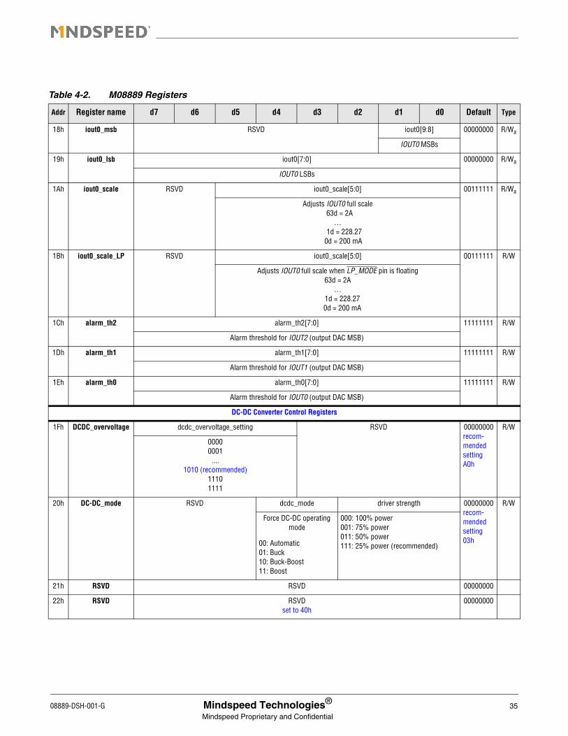
18h iout0_msb RSVD iout0[9:8] 00000000 R/Wa
IOUT0 MSBs
19h iout0_lsb iout0[7:0] 00000000 R/Wa
IOUT0 LSBs
1Ah iout0_scale RSVD iout0_scale[5:0] 00111111 R/Wa
Adjusts IOUT0 full scale 63d = 2A
… 1d = 228.27 0d = 200 mA
1Bh iout0_scale_LP RSVD iout0_scale[5:0] 00111111 R/W
Adjusts IOUT0 full scale when LP_MODE pin is floating63d = 2A
… 1d = 228.27 0d = 200 mA
1Ch alarm_th2 alarm_th2[7:0] 11111111 R/W
Alarm threshold for IOUT2 (output DAC MSB)
1Dh alarm_th1 alarm_th1[7:0] 11111111 R/W
Alarm threshold for IOUT1 (output DAC MSB)
1Eh alarm_th0 alarm_th0[7:0] 11111111 R/W
Alarm threshold for IOUT0 (output DAC MSB)
DC-DC Converter Control Registers
1Fh DCDC_overvoltage dcdc_overvoltage_setting RSVD 00000000recom-mended setting A0h
R/W
00000001
....1010 (recommended)
11101111
20h DC-DC_mode RSVD dcdc_mode driver strength 00000000recom-mended setting 03h
R/W
Force DC-DC operating mode
00: Automatic01: Buck10: Buck-Boost11: Boost
000: 100% power001: 75% power011: 50% power111: 25% power (recommended)
21h RSVD RSVD 00000000
22h RSVD RSVDset to 40h
00000000
Table 4-2. M08889 Registers
Addr Register name d7 d6 d5 d4 d3 d2 d1 d0 Default Type
08889-DSH-001-G Mindspeed Technologies®35
Mindspeed Proprietary and Confidential

23h overtemp overtemp RSVD low_ioutx 00000000 R/W
Over tem-perature
protection 1: Enabled 0: Disabled
Optimize IOUTX per-formance
1: low IOUTX current 0: high IOUTX cur-rent
Power down control for all output stages
11: Output stage always on regardless of Ix_ON signal10: Fast power down 01: Deep sleep when Ix_ON=L00: Deep sleep when Ix_ON=L
24h regref_setup extr_ctrl 7k_res 100k_res regref_mode
RSVD idac_cur dig_RC 0001110 (set this
register to 20h)
R/W
1: Use exter-nal resistor for DC-DC converter control 0: Normal operation
1: 7k Ω 0: 14k Ω
1: 100k Ωrecommended) 0: 14k Ω
DC-DC con-verter con-trol mode 1: Analog control (rec-ommended) 0: Digital control
1: IDAC current 200 µA
0: Normal operation (100 µA)
1: Add 1 µs RC filter to IOUT voltage when in digi-tal control mode
0: Normal operation
25h regref2_dac_MSB RSVD regref2_dac[8]
00000000 R/W
REGREF DAC
IOUT2 MSB
26h regref2_dac regref2_dac[7:0] 00000000 R/W
REGREF DAC. IOUT2 LSBs
27h regref2_ctrl1 headroom2[4:0] (100 mV/Amp, 70 mV min) regref2_dec[2:0] 00000000 R/W
Controls headroom for IOUT200000: 0 mV00001:10 mV00010:20 mV00011:30 mV
….11111:310 mV
Select decimation factor for REGREF2 digital loop: 000: 1 001: 2 010: 4 011: 32 100: 64 101: 256 110: 512 111: 2048 (recommended)
28h regref2_ctrl0 update_rate2[2:0] RSVD rregrefDAC2_init[1:0] regref_wait2[1:0] 00000000 (set this
register to 44h)
R/W
DAC update rate (12.5 MHz clock cycles)
000: No updates 001: 8 010: 512 011: 1024 100: 2048 101: 4096 110: 8192 111: 16374 (equiv. to 1.31 ms)
Initial value of DAC output for IOUT2
01b recommended 00: 0 01: previous value 10: value contained in regref2_dac[8:0] 11: 0
Wait states after I2_ON high before starting
counting (IDAC current is fixed to initial value - this is not impacted by PWM
or MPG)
00: no wait 01: ~20usec 10: ~100usec 11: ~200usec
Table 4-2. M08889 Registers
Addr Register name d7 d6 d5 d4 d3 d2 d1 d0 Default Type
08889-DSH-001-G Mindspeed Technologies®36
Mindspeed Proprietary and Confidential

29h regref1_dac_MSB RSVD regref1_dac[8]
00000000 R/W
REGREF DAC
IOUT1 MSB
2Ah regref1_dac regref1_dac[7:0] 00000000 R/W
REGREF DAC IOUT1 LSBs
2Bh regref1_ctrl1 headroom1[4:0] regref1_dec[2:0] 00000000 R/W
Controls headroom for IOUT100000: 0 mV00001:10 mV00010:20 mV00011:30 mV
….11111:310 mV
Select decimation factor for REGREF1 digital loop: 000: 1 001: 2 010: 4 011: 32 100: 64 101: 256 110: 512 111: 2048 (recommended)
2Ch regref1_ctrl0 update_rate1[2:0] RSVD rregrefDAC1_init[1:0] regref_wait1[1:0] 00000000 (set this
register to 44h)
R/W
DAC update rate (12.5 MHz clock cycles)
000: No updates 001: 8 010: 512 011: 1024 100: 2048 101: 4096 110: 8192 111: 16374 (equiv. to 1.31 ms)
Initial value of DAC output for IOUT1
00: 0 01: previous value 10: value contained in regref1_dac[8:0] 11: 0
Wait states after I1_ON high before enabling
counting (IDAC current is fixed to initial value - this is not impacted by PWM
or MPG) 00: no wait 01: ~20usec 10: ~100usec 11: ~200usec
2Dh regref0_dac_MSB RSVD regref0_dac[7:0]
00000000 R/W
REGREF DAC
IOUT0 MSB
2Eh regref0_dac regref0_dac[7:0] 00000000 R/W
REGREF DAC IOUT0 LSBs
2Fh regref0_ctrl1 headroom0[4:0] regref0_dec[2:0] 00000000 R/W
Controls headroom for IOUT000000: 0 mV00001:10 mV00010:20 mV00011:30 mV
….11111:310 mV
Select decimation factor for REGREF0 digital loop: 000: 1 001: 2 010: 4 011: 32 100: 64 101: 256 110: 512 111: 2048 (recommended)
Table 4-2. M08889 Registers
Addr Register name d7 d6 d5 d4 d3 d2 d1 d0 Default Type
08889-DSH-001-G Mindspeed Technologies®37
Mindspeed Proprietary and Confidential

30h regref0_ctrl0 update_rate0[2:0] RSVD rregrefDAC0_init[1:0] regref_wait0[1:0] 00000000 (set this register to 44h)
R/W
DAC update rate (12.5 MHz clock cycles)
000: No updates 001: 8 010: 512 (recommended) 011: 1024 100: 2048 101: 4096 110: 8192 111: 16374 (equiv. to 1.31 ms)
Initial value of DAC output for channel 0
01b recommended 00: 0 01: previous value 10: value contained in regref0_dac[8:0] 11: 0
Wait states after I_ON before enabling counting (IDAC current is fixed to initial value - this is not impacted by PWM or
MPG) 00: no wait 01: ~20usec 10: ~100usec 11: ~200usec
31h alarm_idac2 alarm_th2[7:0] 11111111 R/W
Alarm threshold for IOUT2 (output DAC MSB)
32h alarm_idac1 alarm_th1[7:0] 11111111 R/W
Alarm threshold for IOUT1 (output DAC MSB)
33h alarm_idac0 alarm_th0[7:0] 11111111 R/W
Alarm threshold for IOUT0 (output DAC MSB)
APC REGISTERS
34h apc_ctrl RSVD loop_select RSVD apc_en2 apc_en1 apc_en0 01000000 R/W
Selects APC type:
1: CPC0: IPC
Enable APC for channel 2 1: APC enabled0: APC dis-abled
Enable APC for channel 1 1: APC enabled0: APC dis-abled
Enable APC for channel 0 1: APC enabled0: APC dis-abled
35h target2_msb RSVD target2[12:8] 00000000 R/Wa
MSB target DAC for gain of IOUT2
36h target2_lsb target2[7:0] 00000000 R/Wa
LSB target DAC for gain of IOUT2
37h target1_msb RSVD target1[12:8] 00000000 R/Wa
MSB target DAC for gain of IOUT1
38h target1_lsb target1[7:0] 00000000 R/Wa
LSB target DAC for gain of IOUT1
39h target0_msb RSVD target0[12:8] 00000000 R/Wa
MSB target DAC for gain of IOUT0
3Ah target0_lsb target0[7:0] 00000000 R/Wa
LSB target DAC for gain of IOUT0
3Bh target2_msb_LP RSVD target2_LP[12:8] 00000000 R/Wa
MSB target DAC for gain of IOUT2 when LP_MODE=L
3Ch target2_lsb_LP target2_LP[7:0] 00000000 R/Wa
LSB target DAC for gain of IOUT2 when LP_MODE=L
Table 4-2. M08889 Registers
Addr Register name d7 d6 d5 d4 d3 d2 d1 d0 Default Type
08889-DSH-001-G Mindspeed Technologies®38
Mindspeed Proprietary and Confidential

3Dh target1_msb_LP RSVD target1_LP[12:8] 00000000 R/Wa
MSB target DAC for gain of IOUT1 when LP_MODE=L
3Eh target1_lsb_LP target1_LP[7:0] 00000000 R/Wa
LSB target DAC for gain of IOUT1 when LP_MODE=L
3Fh target0_msb_LP RSVD target0_LP[12:8] 00000000 R/Wa
MSB target DAC for gain of IOUT0 when LP_MODE=L
40h target0_lsb_LP target0_LP[7:0] 00000000 R/Wa
LSB target DAC for gain of IOUT0 when LP_MODE=L
CPC REGISTERS
41h apc2_ctrl2 Tck_init2[1:0] Tck_mid2[1:0] Tck_min2[1:0] Tck_div2[1:0] 00000000 R/W
Initial clock count for IOUT200: 0
01: 63 10: 127 11: 255
Mid clock count for IOUT200: 0
01: 31 10: 63
11: 127
Clock counts for IOUT2 at min step
00: 0 01: 3110: 63
11: 127
Clock counts to enable clock divider for IOUT2
00: 0 01: 63
10: 127 11: 255
42h apc2_ctrl1 Step_init2[1:0] Step_mid2[1:0] iturnon2 ck_div2[1:0] 00000000 R/W
Initial step size in LSB of IOUT200: 101: 8
10: 1611: 32
Mid step size in LSB of IOUT2 00: 1/2 of Step_init 01: 1/4 of Step_init 10: reserved 11: reserved
Initial value of IOUT2 00: 0 01: previous value 10: value contained in bit iout2[9:0] 11: 0
Clock divider for IOUT2
00: 101: 410: 8
11: 16
43h apc2_ctrl0 Dec2[2:0] RSVD cpc_wait2[1:0] apc2_freeze 00000000 R/W
Digital filter decimation factor for IOUT2:
000: 1001: 2010: 4011: 8
100: 16 101: 32 110: 64
111: 128
Wait states before enabling APC (current is
fixed to initial value) 00: no wait 01: ~20usec 10: ~100usec 11: ~200usec
1: freeze APC for IOUT2 0: normal operation
44h apc1_ctrl2 Tck_init1[1:0] Tck_mid1[1:0] Tck_min1[1:0] Tck_div1[1:0] 00000000 R/W
Initial clock count for IOUT100: 0
01: 6310: 12711: 255
Mid clock count for IOUT100: 001: 3110: 63
11: 127
Clock counts for IOUT1 at min step
00: 001: 3110: 63
11: 127
Clock counts to enable clock divider for IOUT1
00: 001: 6310: 12711: 255
Table 4-2. M08889 Registers
Addr Register name d7 d6 d5 d4 d3 d2 d1 d0 Default Type
08889-DSH-001-G Mindspeed Technologies®39
Mindspeed Proprietary and Confidential

45h apc1_ctrl1 Step_init1[1:0] Step_mid1[1:0] iturnon1 ck_div1[1:0] 00000000 R/W
Initial step size in LSB of IOUT100: 101: 8
10: 1611: 32
Mid step size in LSB of IOUT1
00: 1/2 of Step_init01: 1/4 of Step_init
10: reserved11: reserved
Initial value of IOUT100: 0
01: previous value 10: value contained in bit
iout1[9:0]11: 0
Clock divider for IOUT100: 101: 410: 811: 16
46h apc1_ctrl0 Dec1[2:0] RSVD cpc_wait1[1:0] apc1_freeze 00000000 R/W
Digital filter decimation factor for IOUT1:000: 1001: 2010: 4011: 8
100: 16101: 32110: 64111: 128
Wait states before enabling APC (current is
fixed to initial value)00: no wait01: ~20usec10: ~100usec11: ~200usec
1: freeze APC (both gain and
offset) for IOUT1
: normal operation
47h apc0_ctrl2 Tck_init0[1:0] Tck_mid0[1:0] Tck_min0[1:0] Tck_div0[1:0] 00000000 R/W
Initial clock count for IOUT000: 0
01: 6310: 12711: 255
Mid clock count for IOUT000: 001: 3110: 63
11: 127
Clock counts for IOUT0 at min step
00: 001: 3110: 63
11: 127
Clock counts to enable clock divider for IOUT0
00: 001: 6310: 12711: 255
48h apc0_ctrl1 Step_init0[1:0] Step_mid0[1:0] iturnon0 ck_div0[1:0] 00000000 R/W
Initial step size in LSB of IOUT000: 101: 8
10: 1611: 32
Mid step size in LSB of IOUT0
00: 1/2 of Step_init01: 1/4 of Step_init
10: reserved11: reserved
Initial value of IOUT000: 0
01: previous value 10: value contained in bit
iout0[9:0]11: 0
Clock divider for IOUT000: 101: 410: 811: 16
49h apc0_ctrl0 Dec0[2:0] RSVD cpc_wait0[1:0] apc0_freeze 00000000 R/W
Digital filter decimation factor for IOUT0:000: 1001: 2010: 4011: 8
100: 16101: 32110: 64111: 128
Wait states before enabling APC (current is
fixed to initial value)
00: no wait 01: ~20usec
10: ~100usec 11: ~200usec
1: freeze APC (both gain and offset) for IOUT0 0: normal operation
Table 4-2. M08889 Registers
Addr Register name d7 d6 d5 d4 d3 d2 d1 d0 Default Type
08889-DSH-001-G Mindspeed Technologies®40
Mindspeed Proprietary and Confidential

IPC Setup Registers
4Ah ipc_setup RSVD mirror ratio source_sink
pd_precharge2
pd_precharge1
pd_precharge0
pre_chrg 00000000 R/W
1: 1:1 mir-roring ratio 0: 4x mir-roring ratio
1: Current sinking MPD (pfet input stage) 0: Normal MPD
1: power down pre-charge for APC_IN2 0: Normal operation
1: power down pre-charge for APC_IN1 0: Normal operation
1: power down pre-charge for APC_IN0 0: Normal operation
1: always ON 0: Depends on channel being turned on
4Bh ipc2_ctrl2 RSVD pd_comp RSVD pd_ihelp2 cap2_sel[3:0] 00000001 R/W
1: Power down com-parator 0: Normal operation
Powers down 100 µA helper cur-rent : 1: Power down 0: Normal operation
IPC2 charging capacitor value selector0000 := 25.0 pF0001 := 27.5 pF0010 := 30.0 pF
.........
.........1111 := 62.5 pF
4Ch ipc2_ctrl1 RSVD ipd2_sel[4:0] 00000000 R/W
Peak amplitude monitor photodetector 00000 = 100 µA 00001 = 200 µA
…. 11111 = 3.2 mA
4Dh ipc2_ctrl0 RSVD ich2_sel[4:0] 00000000 R/W
Peak current into IPC2 charging capacitor 00000 = 10 µA 00001 = 20 µA
…. 11111 = 320 µA
4Eh ipc1_ctrl2 RSVD pd_comp hs_sel pd_ihelp1 cap1_sel[3:0] 00000001 R/W
RSVD 1: Power down com-parator 0: Normal operation
1:Increase compara-tor bias current by 66% 0: Normal operation
Powers down 100 µA helper cur-rent : 1: Power down 0: Normal operation
IPC1 charging capacitor value selector0000 := 25.0 pF0001 := 27.5 pF0010 := 30.0 pF
.........
.........1111 := 62.5 pF
4Fh ipc1_ctrl1 RSVD ipd1_sel[4:0] 00000000 R/W
Peak amplitude monitor photodetector 00000 = 100 µA 00001 = 200 µA
…. 11111 = 3.2 mA
Table 4-2. M08889 Registers
Addr Register name d7 d6 d5 d4 d3 d2 d1 d0 Default Type
08889-DSH-001-G Mindspeed Technologies®41
Mindspeed Proprietary and Confidential

50h ipc1_ctrl0 RSVD ich2_sel[4:0] 00000000 R/W
Peak current into IPC1 charging capacitor 00000 = 10 µA 00001 = 20 µA
…. 11111 = 320 µA
51h ipc0_ctrl2 RSVD pd_comp hs_sel pd_ihelp0 cap0_sel[3:0] 00000001 R/W
1: Power down com-parator 0: Normal operation
1:Increase compara-tor bias current by 66% 0: Normal operation
Powers down 100 µA helper cur-rent : 1: Power down 0: Normal operation
IPC0 charging capacitor value selector0000 := 25.0 pF0001 := 27.5 pF0010 := 30.0 pF
.........
.........1111 := 62.5 pF
52h ipc0_ctrl1 RSVD ipd0_sel[4:0] 00000000 R/W
Peak amplitude monitor photodetector 00000 = 100 µA 00001 = 200 µA
…. 11111 = 3.2 mA
53h ipc0_ctrl0 RSVD ich0_sel[4:0] 00000000 R/W
Peak current into IPC0 charging capacitor 00000 = 10 µA 00001 = 20 µA
…. 11111 = 320 µA
TIMER REGISTERS
54h clk_div clk_div_pwm[3:0] clk_div_mpg[3:0] 00000000 R/W
PWM clock divider0000 = 10001 = 20010 = 40011 = 8
0100 = 16 0101 = 32 0110 = 64
0111 = 128
MPG clock divider0000 = 10001 = 20010 = 40011 = 8
0100 = 16 0101 = 32 0110 = 64
0111 = 128
55h pwm_msb RSVD on_count2[9:8] on_count1[9:8] on_count0[9:8] 00000000 R/W
PWM IOUT2 (msb) PWM IOUT1 (msb) PWM IOUT0 (msb)
56h pwm2 on_count2[7:0] 00000000 R/W
PWM on count LSBs for IOUT2
57h pwm1 on_count1[7:0] 00000000 R/W
PWM on count LSBs for IOUT1
58h pwm0 on_count0[7:0] 00000000 R/W
PWM on count LSBs for IOUT0
Table 4-2. M08889 Registers
Addr Register name d7 d6 d5 d4 d3 d2 d1 d0 Default Type
08889-DSH-001-G Mindspeed Technologies®42
Mindspeed Proprietary and Confidential
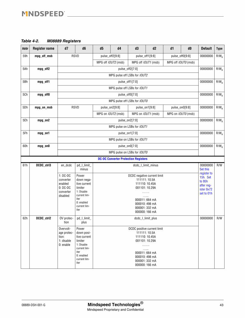
59h mpg_off_msb RSVD pulse_off2[9:8] pulse_off1[9:8] pulse_off0[9:8] 00000000 R/Wa
MPG off IOUT2 (msb) MPG off IOUT1 (msb) MPG off IOUT0 (msb)
5Ah mpg_off2 pulse_off2[7:0] 00000000 R/Wa
MPG pulse off LSBs for IOUT2
5Bh mpg_off1 pulse_off1[7:0] 00000000 R/Wa
MPG pulse off LSBs for IOUT1
5Ch mpg_off0 pulse_off0[7:0] 00000000 R/Wa
MPG pulse off LSBs for IOUT0
5Dh mpg_on_msb RSVD pulse_on2[9:8] pulse_on1[9:8] pulse_on0[9:8] 00000000 R/Wa
MPG on IOUT2 (msb) MPG on IOUT1 (msb) MPG on IOUT0 (msb)
5Eh mpg_on2 pulse_on2[7:0] 00000000 R/Wa
MPG pulse on LSBs for IOUT1
5Fh mpg_on1 pulse_on1[7:0] 00000000 R/Wa
MPG pulse on LSBs for IOUT1
60h mpg_on0 pulse_on0[7:0] 00000000 R/Wa
MPG pulse on LSBs for IOUT0
DC-DC Converter Protection Registers
61h DCDC_ctrl3 en_dcdc pd_I_limit_minus
dcdc_I_limit_minus 00000000Set this register to 15h. Set to 95h after reg-ister 0x72 set to 01h
R/W
1: DC-DC converter enabled 0: DC-DC converter disabled
Power down nega-tive current limiter 1: Disable current lim-iter 0: enabled current lim-iter
DCDC negative current limit111111: 10.5A
111110: 10.45A001101: 10.29A
…….…...
000011: 664 mA000010: 498 mA000001: 332 mA000000: 166 mA
62h DCDC_ctrl2 OV protec-tion
pd_I_limit_plus
dcdc_I_limit_plus 00000000
R/W
Overvolt-age protec-tion: 1: disable 0: enable
Power down posi-tive current limiter 1: Disable current lim-iter 0: enabled current lim-iter
DCDC positive current limit111111: 10.5A
111110: 10.45A001101: 10.29A
…….…...
000011: 664 mA000010: 498 mA000001: 332 mA000000: 166 mA
Table 4-2. M08889 Registers
Addr Register name d7 d6 d5 d4 d3 d2 d1 d0 Default Type
08889-DSH-001-G Mindspeed Technologies®43
Mindspeed Proprietary and Confidential

63h DCDC_ctrl1 fb_int UV protec-tion
dcdc_clk 00001111
R/W
Enables internal feedback network 1: Enabled 0: Use exter-nal feedback network
Under volt-age protec-tion: 1: disable 0: enable
DCDC converter clock frequency111111: 5 MHz +16%011111: 5 MHz +8%
001111: 5 MHz000111: 5 MHz -8%000011: 5 MHz -16%000001: 5 MHz -24%000000: 5 MHz -32%
64h DCDC_ctrl0 dc_ref rf_sel dcdc_clk_div[1:0] dcdc_iout 00000000
R/W
Selects DCDC con-verter refer-ence for headroom voltage 1: regref block 0: 1.2 V Bandgap
Selects feedback resistor value: 1: Rf=1 kΩ 0: Rf=40 kΩ
Select the dcdc clk ratio:00: 1/101: 1/210: 1/311: 1/4
Scales power transistors depending on driver current1111: >1.2A0111: ~1A
0011: ~0.8A0001: ~0.6A
0000: disable all power switches
Color Mixing Registers
65h cm_setup RSVD cm_iout2[1:0] cm_iout1[1:0] cm_iout0[1:0] 00000000
R/W
Defines color mixing when I2_ON=H 00: no color mixing 01: color mixing IOUT0 only using iout0_cm2[9:0] 10: color mixing IOUT1 only using iout1_cm2[9:0] 11: color mixing IOUT0 and IOUT2 using iout0,1_cm2[9:0]
Defines color mixing when I1_ON=H 00: no color mixing 01: color mixing IOUT0 only using iout0_cm1[9:0] 10: color mixing IOUT2 only using iout2_cm1[9:0] 11: color mixing IOUT0 and IOUT2 using iout0,2_cm1[9:0]
Defines color mixing when I0_ON=H 00: no color mixing 01: color mixing IOUT1 only using iout1_cm0[9:0] 10: color mixing IOUT2 only using iout2_cm0[9:0] 11: color mixing IOUT1 and IOUT2 using iout1,2_cm0[9:0]
66h iout2_cm1_msb RSVD iout2_cm1[9:8] 00000000
R/Wa
IOUT2 MSBs (CM1)
67h iout2_cm1_lsb iout2_cm1[7:0] 00000000
R/Wa IOUT2 LSBs for color mixing when I1_ON=H
68h iout2_cm0_msb RSVD iout2_cm0[9:8] 00000000
R/Wa IOUT2 MSBs (CM0)
69h iout2_cm0_lsb iout2_cm0[7:0] 00000000 R/Wa
IOUT2 LSBs for color mixing when I0_ON=H
6Ah iout1_cm2_msb RSVD iout1[9:8] 00000000 R/Wa
IOUT1 MSBs (CM2)
6Bh iout1_cm2_lsb iout1[7:0] 00000000 R/Wa
IOUT1 LSBs for color mixing when I2_ON=H
6Ch iout1_cm0_msb RSVD iout1[9:8] 00000000 R/Wa
IOUT1 MSBs (CM0)
Table 4-2. M08889 Registers
Addr Register name d7 d6 d5 d4 d3 d2 d1 d0 Default Type
08889-DSH-001-G Mindspeed Technologies®44
Mindspeed Proprietary and Confidential

6Dh iout1_cm0_lsb iout1[7:0] 00000000
R/Wa
IOUT1 LSBs for color mixing when I0_ON=H
6Eh iout0_cm2_msb RSVD iout2[9:8] 00000000
R/Wa
IOUT0 MSBs (CM2)
6Fh iout0_cm2_lsb iout2[7:0] 00000000
R/Wa
IOUT0 LSBs for color mixing when I2_ON=H
70h iout0_cm1_msb RSVD iout2[9:8] 00000000
R/Wa
IOUT0 MSBs (CM1)
71h iout0_cm1_lsb iout2[7:0] 00000000
R/Wa
IOUT0 LSBs for color mixing when I1_ON=H
Initialization Registers
72h start_op RSVD start_op 00000000Set this register to 01h.
R/W
1b: Start operation0b: Not
operationalNote: M08889
will not be operational
until 1b is writ-ten
73h soft_reset Soft reset 00000000 R/WSC
Writing AA causes a 16 refclk cycles to reset (self clear after reset)
74h chip_id Revision identification: Chip identification 00111100 R
00 111100
Readback Registers
75h temp temp[7:0] 00000000 R
Temperature readback
76h rb_iout2_msb RSVD rb_iout2[9:8] 00000000 R
Readback IOUT2 DAC MSB
77h rb_iout2_lsb rb_iout2[7:0] 00000000 R
Readback IOUT2 DAC LSB
78h rb_regrefdac2_MSB
RSVD rb_regrefdac2[8]
00000000 R
Readback of
REGREF2 DAC MSB
79h rb_regrefdac2 rb_regrefdac2[7:0] 00000000 R
Readback of REGREF2 DAC :SBs.
Table 4-2. M08889 Registers
Addr Register name d7 d6 d5 d4 d3 d2 d1 d0 Default Type
08889-DSH-001-G Mindspeed Technologies®45
Mindspeed Proprietary and Confidential

7Ah rb_iout1_msb RSVD rb_iout1[9:8] 00000000 R
Readback IOUT1 DAC MSB
7Bh rb_iout1_lsb rb_iout1[7:0] 00000000 R
Readback IOUT1 DAC LSB
7Ch rb_regrefdac2_MSB
RSVD rb_regrefdac1[8]
00000000 R
RSVD Readback of
REGREF1 DAC MSB
7Dh rb_regrefdac1 rb_regrefdac1[7:0] 00000000 R
Readback of REGREF1 DAC.LSBs
7Eh rb_iout0_msb RSVD rb_iout0[9:8] 00000000 R
Readback IOUT0 DAC MSB
7Fh rb_iout0_lsb rb_iout0[7:0] 00000000 R
Readback IOUT0 DAC LSB
80h rb_regrefdac2_MSB
RSVD rb_regrefdac0[8]
00000000 R
RSVD Readback of
REGREF0 DAC MSB
81h rb_regrefdac0 rb_regrefdac0[7:0] 00000000 R
Readback of REGREF0 DAC LSBs.
82h alarm_ctrl cpc_2_alrm cpc_1_alrm cpc_0_alrm regref2_alrm
regref1_alrm
regref0_alrm
RSVD 00000000 R
cpc alarm for IOUT21: alarm0: OK
cpc alarm for IOUT11: alarm0: OK
cpc alarm for IOUT01: alarm0: OK
regref2 IDAC alarm1: alarm0: OK
regref1 IDAC alarm1: alarm0: OK
regref0 IDAC alarm1: alarm0: OK
RSVD
83h alarm_iout ipc_over-shoot
DC-DC overvoltage
I_alrm_neg I_alrm_pos buck_boost_mon
alarm_iout2 alarm_iout1 alarm_iout0 00000000 R
mpd cur-rent too high1: alarm0: OK
DC-DC con-verter over-voltage 1: alarm0: OK
DC-DC Converter negative overcur-rent or the DC-DC out-put is less than 2 V.1: alarm0: OK
DC-DC Converter positive overcurrentThis bit will also assert during an overvolt-
age condi-tion. (see
bit 6)1: alarm0: OK
DC-DC Converter mode mon-itor1: boost0: buck
Open or short on IOUT21: alarm0: OK
Open or short on IOUT11: alarm0: OK
Open or short on IOUT01: alarm0: OK
84h RSVD RSVD 00000000
Table 4-2. M08889 Registers
Addr Register name d7 d6 d5 d4 d3 d2 d1 d0 Default Type
08889-DSH-001-G Mindspeed Technologies®46
Mindspeed Proprietary and Confidential

85h reserved RSVD 00000000
86h strbalrm_ctrl RSVD strb_iout clear_alarm 00000000 R/W
1: strobes iout cur-rent before readback 0: Normal
1: Clear alarm 0: Normal
FEh reserved RSVD 00000000
Table 4-2. M08889 Registers
Addr Register name d7 d6 d5 d4 d3 d2 d1 d0 Default Type
08889-DSH-001-G Mindspeed Technologies®47
Mindspeed Proprietary and Confidential

www.mindspeed.com
General Information:Telephone: (949) 579-3000Headquarters - Newport Beach4000 MacArthur Blvd., East TowerNewport Beach, CA 92660
© 2012 Mindspeed Technologies®, Inc. All rights reserved.
Information in this document is provided in connection with Mindspeed Technologies® ("Mindspeed®") products. These materials are provided by Mindspeed as a service to its customers and may be used for informational purposes only. Except as provided in Mindspeed’s Terms and Conditions of Sale for such products or in any separate agreement related to this document, Mindspeed assumes no liability whatsoever. Mindspeed assumes no responsibility for errors or omissions in these materials. Mindspeed may make changes to specifications and product descriptions at any time, without notice. Mindspeed makes no commitment to update the information and shall have no responsibility whatsoever for conflicts or incompatibilities arising from future changes to its specifications and product descriptions. No license, express or implied, by estoppel or otherwise, to any intellectual property rights is granted by this document.
THESE MATERIALS ARE PROVIDED "AS IS" WITHOUT WARRANTY OF ANY KIND, EITHER EXPRESS OR IMPLIED, RELATING TO SALE AND/OR USE OF MINDSPEED PRODUCTS INCLUDING LIABILITY OR WARRANTIES RELATING TO FITNESS FOR A PARTICULAR PURPOSE, CONSEQUENTIAL OR INCIDENTAL DAMAGES, MERCHANTABILITY, OR INFRINGEMENT OF ANY PATENT, COPYRIGHT OR OTHER INTELLECTUAL PROPERTY RIGHT. MINDSPEED FURTHER DOES NOT WARRANT THE ACCURACY OR COMPLETENESS OF THE INFORMATION, TEXT, GRAPHICS OR OTHER ITEMS CONTAINED WITHIN THESE MATERIALS. MINDSPEED SHALL NOT BE LIABLE FOR ANY SPECIAL, INDIRECT, INCIDENTAL, OR CONSEQUENTIAL DAMAGES, INCLUDING WITHOUT LIMITATION, LOST REVENUES OR LOST PROFITS, WHICH MAY RESULT FROM THE USE OF THESE MATERIALS.
Mindspeed products are not intended for use in medical, lifesaving or life sustaining applications. Mindspeed customers using or selling Mindspeed products for use in such applications do so at their own risk and agree to fully indemnify Mindspeed for any damages resulting from such improper use or sale.
08889-DSH-001-G Mindspeed Technologies®48
Mindspeed Proprietary and Confidential