lvds source synchronous 7:1 serialization and ... - xilinx · summary xilinx ... of 7:1 data in...
TRANSCRIPT
XAPP1315 (v1.0) April 15, 2017 1www.xilinx.com
SummaryXilinx® UltraScale™ and Ultrascale+™ FPGAs contain ISERDESE3 and OSERDESE3 component mode primitives that simplify the design of serializer and deserializer circuits.
This application note describes a component mode solution for the transmission and reception of 7:1 data in UltraScale and UltraScale+ HP IOs and HR I/Os. It describes the use of ISERDESE3 and OSERDESE3 primitives in conjunction with a mixed-mode clock manager (MMCM) or phase-locked loop (PLL) for reception and transmission of 7:1 data using low-voltage differential signaling (LVDS) for data transmission speeds of 415 Mb/s up to 1,100 Mb/s per line in HP I/Os and 1000 Mb/s in HR I/OS.
Download the reference design files for this application note from the Xilinx website. For detailed information about the design files, see Reference Design.
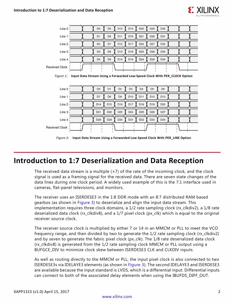
Receiver OverviewThe type of 1:7 interfaces shown in Figure 1 and Figure 2 (5-line interfaces shown) are widely used in consumer devices such as televisions and Blu-ray players for video processing when passing data between components. One video channel typically comprises five LVDS data lines and one LVDS clock line. Modern televisions can use multiple channels (typically four or eight), to ensure adequate video bandwidth. Data framing per line can be achieved in two different ways as shown in Figure 1 and Figure 2.
This application note provides a reference design for both single-channel and multi-channel designs. There is a single pixel clock per channel, and each channel uses one clock multiplication element (MMCM or PLL). The receiver is parameterizable for the number of LVDS data lines per channel. A variable also determines the data framing type of the received data (PER_CLOCK or PER_LINE).
All lines of the same channel must be in the same bank. Each bank supports up to three channels, using a combination of one MMCM and two PLLs. The input pixel clock, generating internal clocks for all data lines in the channel, must be placed on global clock-capable I/O pins.
Application Note: UltraScale and UltraScale+ FPGAs
XAPP1315 (v1.0) April 15, 2017
LVDS Source Synchronous 7:1 Serialization and Deserialization Using Clock MultiplicationAuthors: Ed McGettigan, Kavitha Nagarajan
Introduction to 1:7 Deserialization and Data Reception
XAPP1315 (v1.0) April 15, 2017 2www.xilinx.com
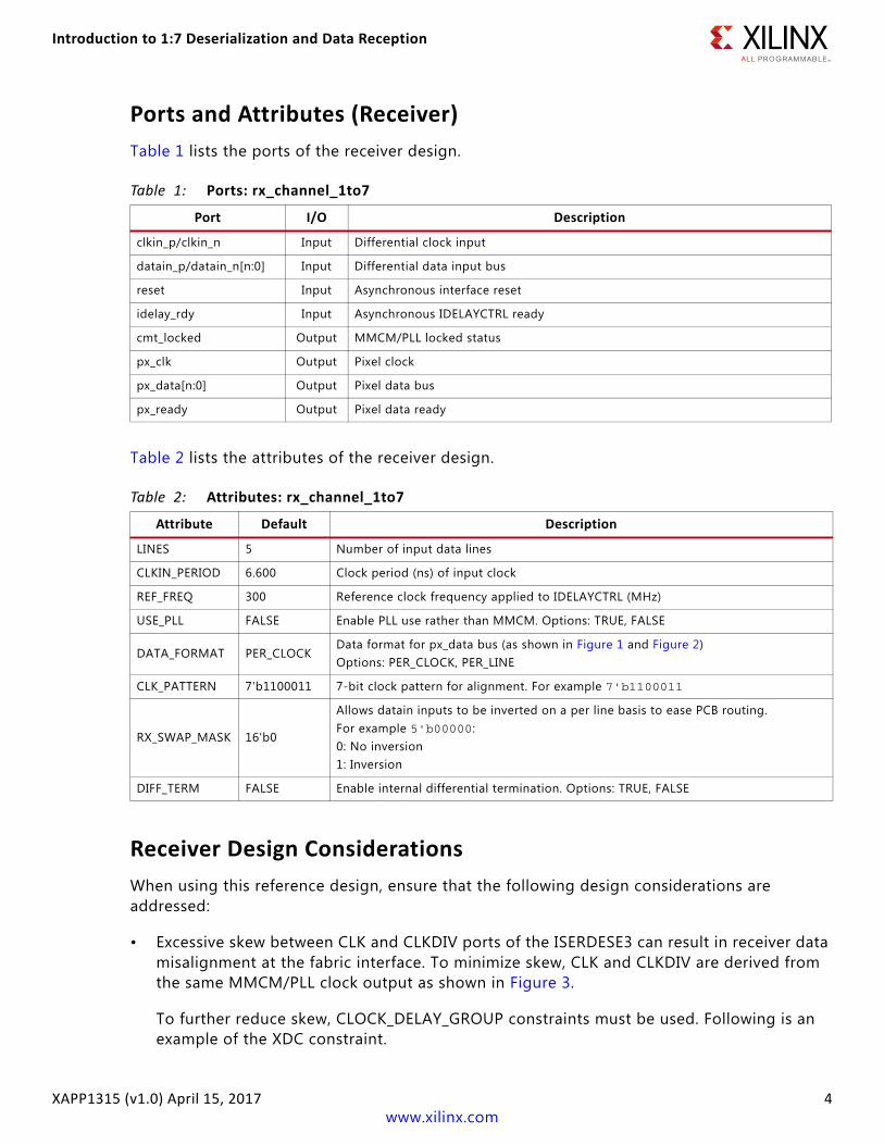
Introduction to 1:7 Deserialization and Data ReceptionThe received data stream is a multiple (×7) of the rate of the incoming clock, and the clock signal is used as a framing signal for the received data. There are seven state changes of the data lines during one clock period. A widely used example of this is the 7:1 interface used in cameras, flat-panel televisions, and monitors.
The receiver uses an ISERDESE3 in the 1:8 DDR mode with an 8:7 distributed RAM based gearbox (as shown in Figure 3) to deserialize and align the input data stream. This implementation requires three clock domains, a 1/2 rate sampling clock (rx_clkdiv2), a 1/8 rate deserialized data clock (rx_clkdiv8), and a 1/7 pixel clock (px_clk) which is equal to the original receiver source clock.
The receiver source clock is multiplied by either 7 or 14 in an MMCM or PLL to meet the VCO frequency range, and then divided by two to generate the 1/2 rate sampling clock (rx_clkdiv2) and by seven to generate the fabric pixel clock (px_clk). The 1/8 rate deserialized data clock (rx_clkdiv8) is generated from the 1/2 rate sampling clock MMCM or PLL output using a BUFGCE_DIV to minimize clock skew between ISERDESE3 CLK and CLKDIV inputs.
As well as routing directly to the MMCM or PLL, the input pixel clock is also connected to two ISERDESE3s via IDELAYE3 elements (as shown in Figure 3). The second IDELAYE3 and ISERDESE3 are available because the input standard is LVDS, which is a differential input. Differential inputs can connect to both of the associated delay elements when using the IBUFDS_DIFF_OUT.
X-Ref Target - Figure 1
Figure 1: Input Data Stream Using a Forwarded Low-Speed Clock With PER_CLOCK Option
X-Ref Target - Figure 2
Figure 2: Input Data Stream Using a Forwarded Low-Speed Clock With PER_LINE Option

Introduction to 1:7 Deserialization and Data Reception
XAPP1315 (v1.0) April 15, 2017 3www.xilinx.com
The initial delay of the master delay is set to be zero. The slave delay is set to be offset by a half-bit period. By incrementing the delays, sampling, and comparing the master and slave bits, the calibration state machine determines the ideal delay for the DDR sampling clock. After this process is complete, the calibrated delay value is broadcast to all the data lines in the channel. At this point, the calibration state machine completes, and no further adjustments are made.
Data word alignment and 8:7 conversion is managed in the gearbox and, after it is determined for the pixel clock data line, it is broadcast to the rest of the data lines.
An illustration of the receiver implementation is shown in Figure 3:
X-Ref Target - Figure 3
Figure 3: Data Reception
PLL/MMCMBUFG
BUFG
BUFGCE_DIV
IDELAYE3
IDELAYE3
ISERDESE3
ISERDESE3
CLKDIV
CLKReceiver Pixel Clock
LVDS CLOCK Channel 0 8
8
IDELAYE3
IDELAYE3Gearbox
8
8
LVDS Data Channel 0
Data Lines
CLKIN
Clock
CLOCK_PCLOCK_N
DATA_P
DATA_N
CLKFBIN
CHANNEL 0
IDELAYCTRLREFCLK
PLL/MMCM
IBUFDS_DIFF_OUT
BUFG
BUFG
BUFGCE_DIV
IDELAYE3
IDELAYE3
ISERDESE3
ISERDESE3
Calibration SM and Gearbox
CLKDIV
CLKReceiver Pixel Clock
LVDS CLOCK Channel 1 8
8
IDELAYE3
IDELAYE3
ISERDESE3
ISERDESE3Gearbox
8
8
LVDS Data Channel 1
Data Lines
CLKIN
CLOCK_P
CLOCK_N
DATA_PDATA_N
CLKFBIN
CHANNEL 1
7-bit Data toFabric
IBUFDS_DIFF_OUT
ISERDESE3
ISERDESE3
IBUFDS_DIFF_OUT
IBUFDS_DIFF_OUT
Calibration SM and Gearbox
7-bit Data toFabric
Introduction to 1:7 Deserialization and Data Reception
XAPP1315 (v1.0) April 15, 2017 4www.xilinx.com
Ports and Attributes (Receiver)
Table 1 lists the ports of the receiver design.
Table 2 lists the attributes of the receiver design.
Receiver Design Considerations
When using this reference design, ensure that the following design considerations are addressed:
• Excessive skew between CLK and CLKDIV ports of the ISERDESE3 can result in receiver data misalignment at the fabric interface. To minimize skew, CLK and CLKDIV are derived from the same MMCM/PLL clock output as shown in Figure 3.
To further reduce skew, CLOCK_DELAY_GROUP constraints must be used. Following is an example of the XDC constraint.
Table 1: Ports: rx_channel_1to7
Port I/O Description
clkin_p/clkin_n Input Differential clock input
datain_p/datain_n[n:0] Input Differential data input bus
reset Input Asynchronous interface reset
idelay_rdy Input Asynchronous IDELAYCTRL ready
cmt_locked Output MMCM/PLL locked status
px_clk Output Pixel clock
px_data[n:0] Output Pixel data bus
px_ready Output Pixel data ready
Table 2: Attributes: rx_channel_1to7
Attribute Default Description
LINES 5 Number of input data lines
CLKIN_PERIOD 6.600 Clock period (ns) of input clock
REF_FREQ 300 Reference clock frequency applied to IDELAYCTRL (MHz)
USE_PLL FALSE Enable PLL use rather than MMCM. Options: TRUE, FALSE
DATA_FORMAT PER_CLOCKData format for px_data bus (as shown in Figure 1 and Figure 2)Options: PER_CLOCK, PER_LINE
CLK_PATTERN 7'b1100011 7-bit clock pattern for alignment. For example 7'b1100011
RX_SWAP_MASK 16'b0
Allows datain inputs to be inverted on a per line basis to ease PCB routing.For example 5'b00000:0: No inversion1: Inversion
DIFF_TERM FALSE Enable internal differential termination. Options: TRUE, FALSE

Introduction to 1:7 Deserialization and Data Reception
XAPP1315 (v1.0) April 15, 2017 5www.xilinx.com
This constraint must be unique for each rx_channel_1to7 module. The constraint must have a unique name (for example, ioclockGroup_rx1) and correct hierarchical instance name (for example, rx_channel1).
set_property CLOCK_DELAY_GROUP ioclockGroup_rx1 [get_nets {rx_channel1/rx_clkdiv*}]
• Certain paths within the receiver are not required to be timed, and should be marked as a false path to achieve timing closure. Following is an example of the XDC constraints. The correct hierarchical instance name, for example, rx_channel1, for the rx_channel_1to7 module must be used.
set_false_path -to [get_pins {rx_channel1/rxc_gen/iserdes_m/D}]set_false_path -to [get_pins {rx_channel1/rxc_gen/iserdes_s/D}]set_false_path -to [get_pins {rx_channel1/rxc_gen/px_reset_sync_reg[*]/PRE}] set_false_path -to [get_pins {rx_channel1/rxc_gen/px_rx_ready_sync_reg[*]/CLR}] set_false_path -to [get_pins {rx_channel1/rxc_gen/px_data_reg[*]/D}]set_false_path -to [get_pins {rx_channel1/rxc_gen/px_rd_last_reg[*]/D}]set_false_path -to [get_pins {rx_channel1/rxd[*].sipo/px_data_reg[*]/D}]set_false_path -to [get_pins {rx_channel1/rxd[*].sipo/px_rd_last_reg[*]/D}]
• For the calibration algorithm to have an accurate reading of the bit time, an IDELAYCTRL block must be instantiated at the top level of the design, with its RDY output connected to the idelay_rdy ports of each rx_channel_7to1 instantiation. An example instantiation is shown below. The IDELAYCTRL block requires a 200–800 MHz clock input. The frequency of this clock (MHz) is provided as the value of the attribute REF_FREQ to the rx_channel_7to1 block.
The reset of the IDELAYCTRL block (RST) must be deasserted after asynchronous resets to the rx_channel_7to1 instantiations are released and the receiver MMCM/PLLs are locked.
//// Idelay control block//IDELAYCTRL #( // Instantiate input delay control block .SIM_DEVICE ("ULTRASCALE")) icontrol ( .REFCLK (clk300_g),// reference clock to IDELAYCTRL (Range = 200.0 to 800.0 Mhz)
.RST (idly_reset_int), //asynchronous reset to IDELAYCTRL .RDY (rx_idelay_rdy) //connect to idelay_rdy port of all rx_channel_7to1 instantiations );assign idly_reset_int = rx_reset | !rx1_cmt_locked | !rx2_cmt_locked;
Reset Sequence
The following reset sequence is required:
1. Deassert rx_channel_1to7 resets.
2. Wait for MMCM/PLL locks to assert.
3. Deassert IDELAYCTRL reset.
4. The px_data output bus is valid when px_ready asserts.
Introduction to Serialization and Data Transmission
XAPP1315 (v1.0) April 15, 2017 6www.xilinx.com
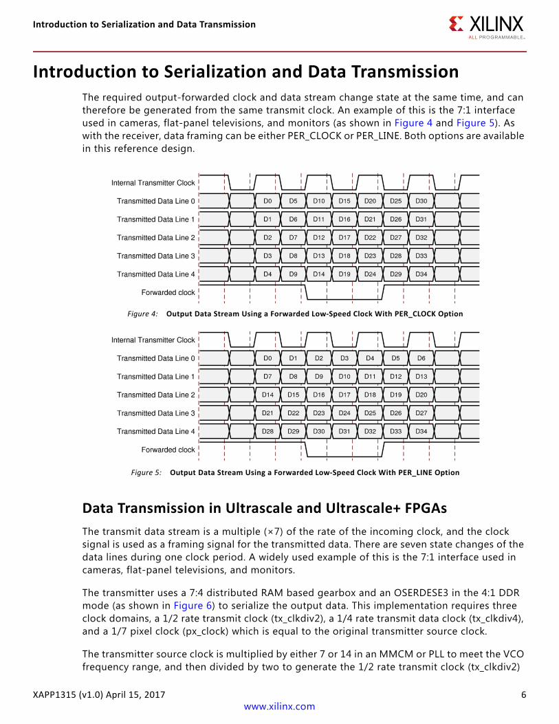
Introduction to Serialization and Data TransmissionThe required output-forwarded clock and data stream change state at the same time, and can therefore be generated from the same transmit clock. An example of this is the 7:1 interface used in cameras, flat-panel televisions, and monitors (as shown in Figure 4 and Figure 5). As with the receiver, data framing can be either PER_CLOCK or PER_LINE. Both options are available in this reference design.
Data Transmission in Ultrascale and Ultrascale+ FPGAs
The transmit data stream is a multiple (×7) of the rate of the incoming clock, and the clock signal is used as a framing signal for the transmitted data. There are seven state changes of the data lines during one clock period. A widely used example of this is the 7:1 interface used in cameras, flat-panel televisions, and monitors.
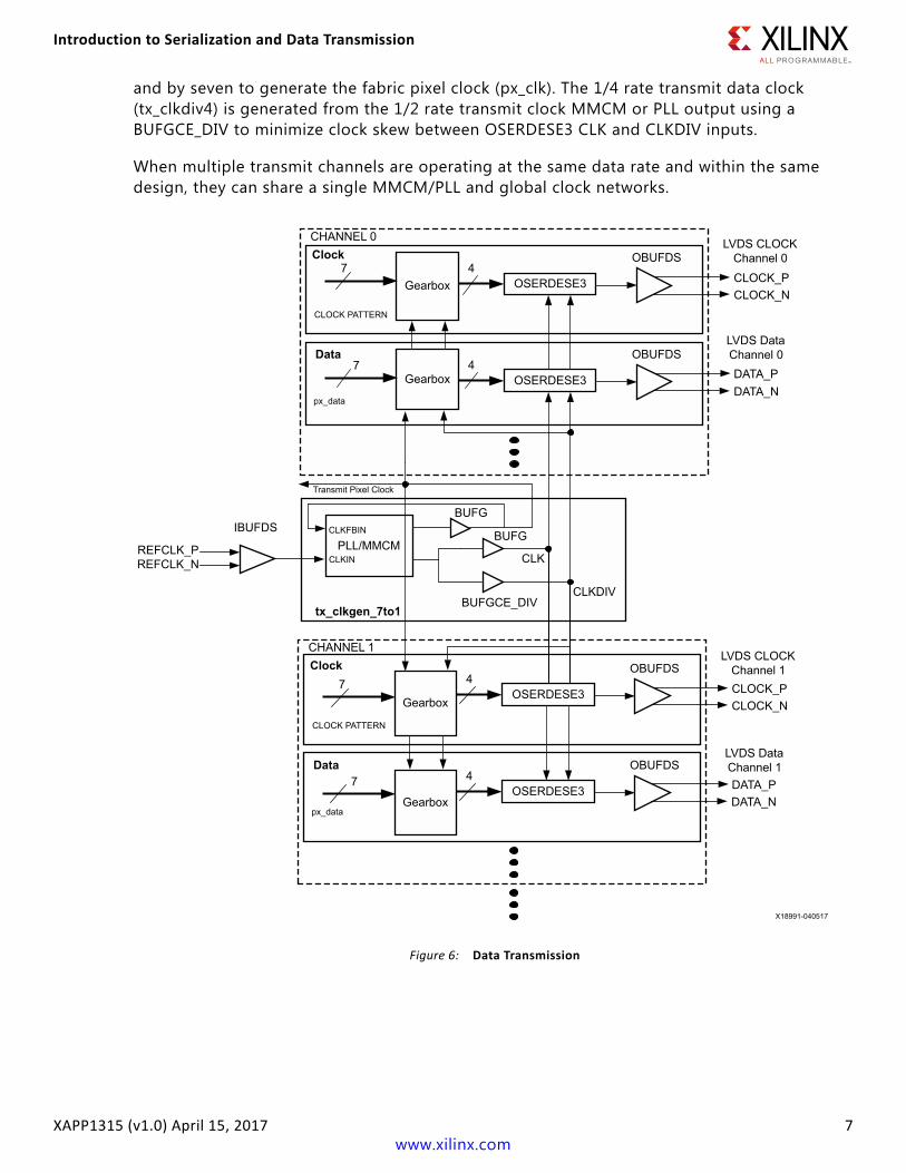
The transmitter uses a 7:4 distributed RAM based gearbox and an OSERDESE3 in the 4:1 DDR mode (as shown in Figure 6) to serialize the output data. This implementation requires three clock domains, a 1/2 rate transmit clock (tx_clkdiv2), a 1/4 rate transmit data clock (tx_clkdiv4), and a 1/7 pixel clock (px_clock) which is equal to the original transmitter source clock.
The transmitter source clock is multiplied by either 7 or 14 in an MMCM or PLL to meet the VCO frequency range, and then divided by two to generate the 1/2 rate transmit clock (tx_clkdiv2)
X-Ref Target - Figure 4
Figure 4: Output Data Stream Using a Forwarded Low-Speed Clock With PER_CLOCK Option
X-Ref Target - Figure 5
Figure 5: Output Data Stream Using a Forwarded Low-Speed Clock With PER_LINE Option
Introduction to Serialization and Data Transmission
XAPP1315 (v1.0) April 15, 2017 7www.xilinx.com
and by seven to generate the fabric pixel clock (px_clk). The 1/4 rate transmit data clock (tx_clkdiv4) is generated from the 1/2 rate transmit clock MMCM or PLL output using a BUFGCE_DIV to minimize clock skew between OSERDESE3 CLK and CLKDIV inputs.
When multiple transmit channels are operating at the same data rate and within the same design, they can share a single MMCM/PLL and global clock networks.
X-Ref Target - Figure 6
Figure 6: Data Transmission
PLL/MMCM
OBUFDS
BUFG
OSERDESE3Gearbox
LVDS CLOCK Channel 0
7 4Clock
CLOCK_PCLOCK_N
CHANNEL 0
CLOCK PATTERN
OSERDESE3Gearbox4
px_data
Data7
OBUFDSLVDS Data Channel 0DATA_PDATA_N
CLKFBIN
CLKIN
BUFG
BUFGCE_DIVtx_clkgen_7to1
Transmit Pixel Clock
CLK
CLKDIV
IBUFDS
REFCLK_PREFCLK_N
OBUFDS
OSERDESE3Gearbox
LVDS CLOCK Channel 1
7 4Clock
CLOCK_PCLOCK_N
CHANNEL 1
CLOCK PATTERN
OSERDESE3Gearbox
4
px_data
Data7
OBUFDSLVDS Data Channel 1DATA_PDATA_N

Introduction to Serialization and Data Transmission
XAPP1315 (v1.0) April 15, 2017 8www.xilinx.com
Ports and Attributes (Transmitter)
Table 3 lists the ports of the transmitter channel (tx_channel_7to1.v).
Table 4 list the attributes of the transmitter channel (tx_channel_7to1.v).
Table 5 lists the ports of the transmitter clock generator (tx_clkgen_7to1.v).
Table 6 list the attributes of the transmitter clock generator (tx_clkgen_7to1.v).
Table 3: Ports: tx_channel_7to1.v
Port I/O Description
tx_clk_p/tx_clk_n Output Differential clock output
tx_out_p/tx_out_n[n:0] Output Differential data output bus
px_data[n:0] Input Pixel data bus, synchronous to px_clk
px_reset Input Reset for pixel logic, synchronous to px_clk
px_clk Input Pixel clock running at 1/7 transmit rate
tx_clkdiv2 Input Transmit clock running at 1/2 transmit rate (CLK input to OSERDESE3)
tx_clkdiv4 Input Transmit clock running at 1/4 transmit rate (CLKDIV input to OSERDESE3)
Table 4: Attributes: tx_channel_7to1.v
Attribute Default Description
LINES 5 Number of output data lines
DATA_FORMAT PER_CLOCKData format for px_data bus (as shown in Figure 4 and Figure 5)Options: PER_CLOCK, PER_LINE
CLK_PATTERN 7'b11000111 Transmit clock bit pattern. For example: 7'b1100011
TX_SWAP_MASK 16'b0
Allows dataout outputs to be inverted on a per line basis to ease PCB routing.For example 5'b00000:0: No inversion1: Inversion
Table 5: Ports: tx_clkgen_7to1.v
Port I/O Description
clkin Input Transmit pixel clock
reset Input Asynchronous interface reset
px_clk Output Pixel clock running at 1/7 transmit rate
tx_clkdiv2 Output Transmit clock divide by two (px_clk * 3.50)
tx_clkdiv4 Output Transmit clock divide by four (px_clk * 1.75)
cmt_locked Output MMCM/PLL locked output
Table 6: Attributes: tx_clkgen_7to1.v
Attribute Default Description
CLKIN_PERIOD 6.600 Clock period (ns) of transmit clock
USE_PLL FALSE Enable PLL use rather than MMCM. Options: TRUE, FALSE

Introduction to Serialization and Data Transmission
XAPP1315 (v1.0) April 15, 2017 9www.xilinx.com
Transmitter Design Considerations
When using this reference design, ensure that the following design considerations are addressed:
• Excessive skew between CLK and CLKDIV ports of the OSERDESE3 can result in transmit data misalignment. To minimize the skew, CLK and CLKDIV are derived from the same MMCM/PLL clock output in the reference design as shown in Figure 6.
To further reduce skew, CLOCK_DELAY_GROUP constraints must be used. Following is an example of the XDC constraints. The correct hierarchical instance name (for example, tx_clkgen for the tx_clkgen_7to_1 module) must be used. If multiple tx_clkgen_7to1 modules are used, the constraint must have a unique name (for example, ioclockGroup_tx) for each module:
set_property CLOCK_DELAY_GROUP ioclockGroup_tx [get_nets -of [get_pins tx_clkgen/bg_txdiv2/O]]set_property CLOCK_DELAY_GROUP ioclockGroup_tx [get_nets -of [get_pins tx_clkgen/bg_txdiv4/O]]
• Certain paths within the transmitter are not required to be timed and should be marked as a false path to achieve timing closure. Following is an example of the XDC constraints. The correct hierarchical instance name (for example, tx_channel1 for the tx_channel_1to7 module) must be used.
set_false_path -to [get_pins {tx_channel1/tx_enable_sync_reg[*]/CLR}]set_false_path -to [get_pins {tx_channel1/txc_piso/tx_data_reg[*]/D}]set_false_path -to [get_pins {tx_channel1/txc_piso/rd_last_reg[*]/D}]set_false_path -to [get_pins {tx_channel1/txd[*].piso/tx_data_reg[*]/D}]set_false_path -to [get_pins {tx_channel1/txd[*].piso/rd_last_reg[*]/D}]
Reset Sequence
The following reset sequence is required:
1. Deassert resets to the MMCM/PLL (tx_clkgen_7to1.v).
2. Wait for MMCM/PLL locks to assert.
3. Invert and synchronize the MMCM/PLL locked output to px_clock, and apply to the reset input of each tx_channel_7to1.

Reference Design
XAPP1315 (v1.0) April 15, 2017 10www.xilinx.com
Reference DesignDownload the reference design files for this application note from the Xilinx website. The files are only available in Verilog.
The name of the appropriate file is included in the figures for different methodologies shown throughout this document. Also included are example top-level files and example timing constraints for the 7:1 interface used in flat-panel displays and cameras.
The files included in the reference design are shown in Table 7.
Table 8 shows the reference design matrix.
Table 7: Reference Design Files
/Verilog_src /Verilog_sim /Verilog_example
tx_channel_7to1.v test_txrx_0525m.v top_txrx_0525m.v
tx_clkgen_7to1.v test_txrx_1050m.v top_txrx_0525.xdc
tx_piso_7to1.v top_txrx_1050m.v
rx_channel_1to7.v top_txrx_1050m.xdc
rx_clkgen_1to7.v
rx_sipo_1to7.v
Table 8: Reference Design Matrix
Parameter Description
General
Developer name Xilinx
Target devices Ultrascale and Ultrascale+ FPGAs
Source code provided Yes
Source code format Verilog
Design uses code and IP from existing Xilinx application note and reference designs or third party
No
Simulation
Functional simulation performed Yes
Timing simulation performed No
Test bench used for functional and timing simulations
Yes
Test bench format Verilog
Simulator software/version used XSIM
SPICE/IBIS simulations No
Implementation
Synthesis software tools/versions used Vivado synthesis

Conclusion
XAPP1315 (v1.0) April 15, 2017 11www.xilinx.com
ConclusionUltrascale and Ultrascale+ FPGAs perform in a wide variety of applications requiring serialization and deserialization factors of 7:1 at speeds from 415 Mb/s to 1,100 Mb/s per line for HP I/Os and 1000 Mb/s for HR I/Os.
References1. UltraScale Architecture SelectIO Resources (UG571)
2. LVDS Source Synchronous 7:1 Serialization and Deserialization Using Clock Multiplication (XAPP585)
Revision HistoryThe following table shows the revision history for this document.
Implementation software tools/versions used Vivado® Design Suite 2016.4
Static timing analysis performed Yes
Hardware Verification
Hardware verified Yes
Hardware platform used for verification KCU105 evaluation board with FMC-XM107 loopback card
Table 8: Reference Design Matrix (Cont’d)
Parameter Description
Date Version Revision
04/15/2017 1.0 Initial Xilinx release.
Please Read: Important Legal Notices
XAPP1315 (v1.0) April 15, 2017 12www.xilinx.com
Please Read: Important Legal NoticesThe information disclosed to you hereunder (the “Materials”) is provided solely for the selection and use of Xilinx products. To the maximum extent permitted by applicable law: (1) Materials are made available "AS IS" and with all faults, Xilinx hereby DISCLAIMS ALL WARRANTIES AND CONDITIONS, EXPRESS, IMPLIED, OR STATUTORY, INCLUDING BUT NOT LIMITED TO WARRANTIES OF MERCHANTABILITY, NON-INFRINGEMENT, OR FITNESS FOR ANY PARTICULAR PURPOSE; and (2) Xilinx shall not be liable (whether in contract or tort, including negligence, or under any other theory of liability) for any loss or damage of any kind or nature related to, arising under, or in connection with, the Materials (including your use of the Materials), including for any direct, indirect, special, incidental, or consequential loss or damage (including loss of data, profits, goodwill, or any type of loss or damage suffered as a result of any action brought by a third party) even if such damage or loss was reasonably foreseeable or Xilinx had been advised of the possibility of the same. Xilinx assumes no obligation to correct any errors contained in the Materials or to notify you of updates to the Materials or to product specifications. You may not reproduce, modify, distribute, or publicly display the Materials without prior written consent. Certain products are subject to the terms and conditions of Xilinx’s limited warranty, please refer to Xilinx’s Terms of Sale which can be viewed at https://www.xilinx.com/legal.htm#tos; IP cores may be subject to warranty and support terms contained in a license issued to you by Xilinx. Xilinx products are not designed or intended to be fail-safe or for use in any application requiring fail-safe performance; you assume sole risk and liability for use of Xilinx products in such critical applications, please refer to Xilinx’s Terms of Sale which can be viewed at https://www.xilinx.com/legal.htm#tos.AUTOMOTIVE APPLICATIONS DISCLAIMERAUTOMOTIVE PRODUCTS (IDENTIFIED AS "XA" IN THE PART NUMBER) ARE NOT WARRANTED FOR USE IN THE DEPLOYMENT OF AIRBAGS OR FOR USE IN APPLICATIONS THAT AFFECT CONTROL OF A VEHICLE ("SAFETY APPLICATION") UNLESS THERE IS A SAFETY CONCEPT OR REDUNDANCY FEATURE CONSISTENT WITH THE ISO 26262 AUTOMOTIVE SAFETY STANDARD ("SAFETY DESIGN"). CUSTOMER SHALL, PRIOR TO USING OR DISTRIBUTING ANY SYSTEMS THAT INCORPORATE PRODUCTS, THOROUGHLY TEST SUCH SYSTEMS FOR SAFETY PURPOSES. USE OF PRODUCTS IN A SAFETY APPLICATION WITHOUT A SAFETY DESIGN IS FULLY AT THE RISK OF CUSTOMER, SUBJECT ONLY TO APPLICABLE LAWS AND REGULATIONS GOVERNING LIMITATIONS ON PRODUCT LIABILITY.© Copyright 2017 Xilinx, Inc. Xilinx, the Xilinx logo, Artix, ISE, Kintex, Spartan, Virtex, Vivado, Zynq, and other designated brands included herein are trademarks of Xilinx in the United States and other countries. All other trademarks are the property of their respective owners.