ltv-480 series product data sheet photocoupler...propaga tion delay time to high output level tp lh...
TRANSCRIPT

LITE-ON DCC
RELEASE
LITE-ON Technology Corp. / OptoelectronicsNo.90,Chien 1 Road, Chung Ho, New Taipei City 23585, Taiwan, R.O.C.
Tel: 886-2-2222-6181 Fax: 886-2-2221-1948 / 886-2-2221-0660http://www.liteon.com/opto
PhotocouplerProduct Data SheetLTV-480 series Spec No.: DS70-2016-0064Effective Date: 11/01/2016
Revision: -
BNS-OD-FC001/A4
BNS-OD-FC001/A4
BNS-OD-FC001/A4
BNS-OD-FC001/A4

1/13
PHOTOCOUPLER
LTV-480 series
Part No.: LTV-480 series BNS-OD-FC002/A4 Rev.: A
LTV-480 series
Positive Logic High CMR Intelligent Power Module and Gate Drive Interface Photocoupler
1. Description
The LTV-480 series fast speed photocoupler contains a AlGaAs LED and photo detector with built-in Schmitt trigger to provide
logic-compatible waveforms, eliminating the need for additional wave shaping. The totem pole output eliminates the need for a pull up
resistor and allows for direct drive Intelligent Power Module or gate drive. Minimized propagation delay difference between devices makes
these optocouplers excellent solutions for improving inverter efficiency through reduced switching dead time.
Truth Table
LED OUT
ON H
OFF L
A 0.1μF bypass Capacitor must be
connected between Pin4 and Pin6
Features
Positive output type (totem pole output)
Truth Table Guaranteed: VCC from 4.5V to 30V
Performance Specified for Common IPM Applications Over
Industrial Temperature Range.
Short Maximum Propagation Delays
Minimized Pulse Width Distortion (PWD)
Very High Common Mode Rejection (CMR)
Hysteresis
Safety approval
– UL 1577 recognized with 5000 VRMS for 1 minute for
LTV-480P and LTV-480W
– VDE DIN EN 60747-5-5 Approved
VIORM = 891Vpeak for LTV-480P
VIORM = 1140Vpeak for LTV-480W
Specification
Wide operating temperature range: -40oC to 105oC
Maximum propagation delay tPLH / tPHL = 200/220 ns
Maximum Pulse Width Distortion (PWD) = 120 ns
Propagation Delay Difference Min/Max = -210/210 ns
Wide Operating VCC Range: 4.5 to 30Volts
20 kV/μs minimum common mode rejection (CMR) at
VCM = 1500 V
Applications
IPM Interface Isolation
Isolated IGBT/MOSFET Gate Drive
AC and Brushless DC Motor Drives
Industrial Inverters
General Digital Isolation
Anode
Cathode
V
Vo
GND
DD1 6
5
3 4
Pulse GenV
Vo
CC1 6
5
3 4
I F
0.1μF
CL
V
Vo
CC1 6
2 5
3 4
I F
0.1μF
Pulse Gen Z=50Ω
SHIELD
SHIELD
2
tr = tf = 5nsf =100 kHZ
10% DUTY CYCLE
Vo=5V
Zo=50
2
SHIELD
2/13
PHOTOCOUPLER
LTV-480 series
Part No.: LTV-480 series BNS-OD-FC002/A4 Rev.: A
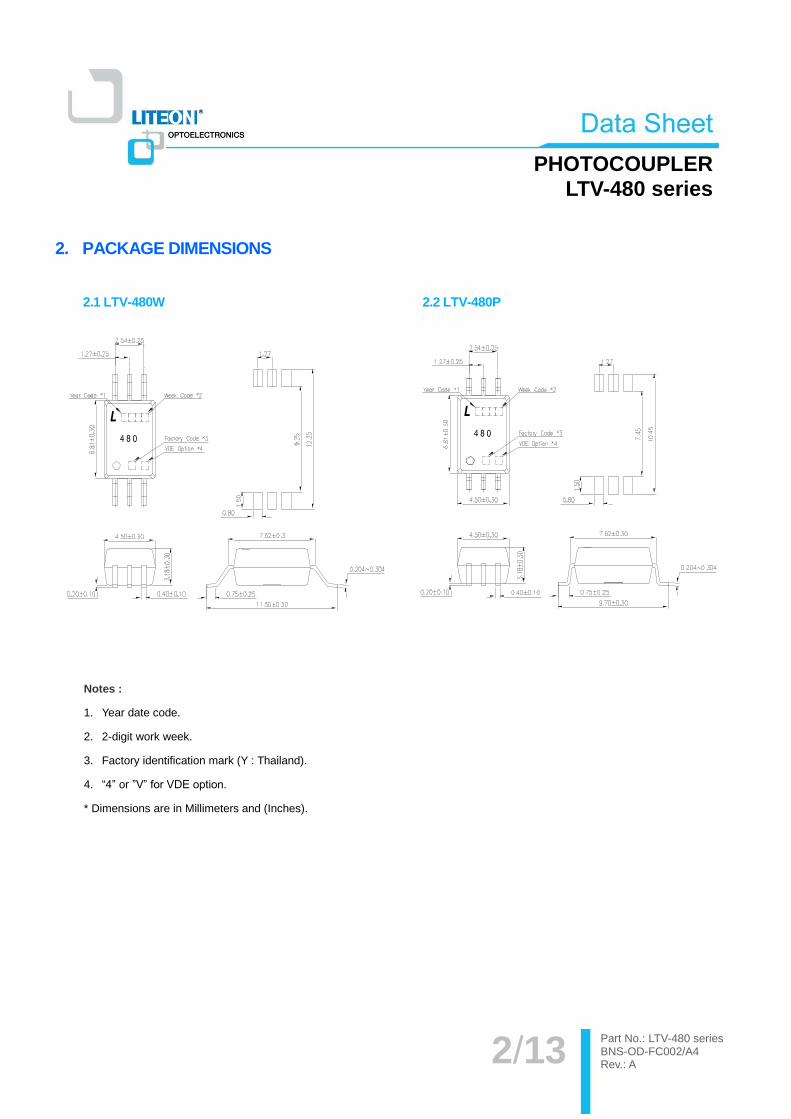
2. PACKAGE DIMENSIONS
2.1 LTV-480W 2.2 LTV-480P
Notes :
1. Year date code.
2. 2-digit work week.
3. Factory identification mark (Y : Thailand).
4. ―4‖ or ‖V‖ for VDE option.
* Dimensions are in Millimeters and (Inches).

3/13
PHOTOCOUPLER
LTV-480 series
Part No.: LTV-480 series BNS-OD-FC002/A4 Rev.: A
3. TAPING DIMENSIONS
3.1 LTV-480W-TA 3.2 LTV-480W-TA1
3.3 LTV-480P-TA 3.4 LTV-480P-TA1
3.5 Quantities Per Reel
Description Symbol Dimension in mm (inch)
For W type
Dimension in mm (inch)
For P type
Tape wide W 16±0.3 (0.63) 16±0.3 (0.63)
Pitch of sprocket holes P0 4±0.1 (0.16) 4±0.1 (0.16)
Distance of compartment
F 7.5±0.1 (0.3) 7.5±0.1 (0.3)
P2 2±0.1 (0.079) 2±0.1 (0.079)
Distance of compartment to compartment P1 16±0.1 (0.63) 12±0.1 (0.47)
Package Type LTV-480 series
Quantities (pcs) 1000
4/13
PHOTOCOUPLER
LTV-480 series
Part No.: LTV-480 series BNS-OD-FC002/A4 Rev.: A
4. RATING AND CHARACTERISTICS
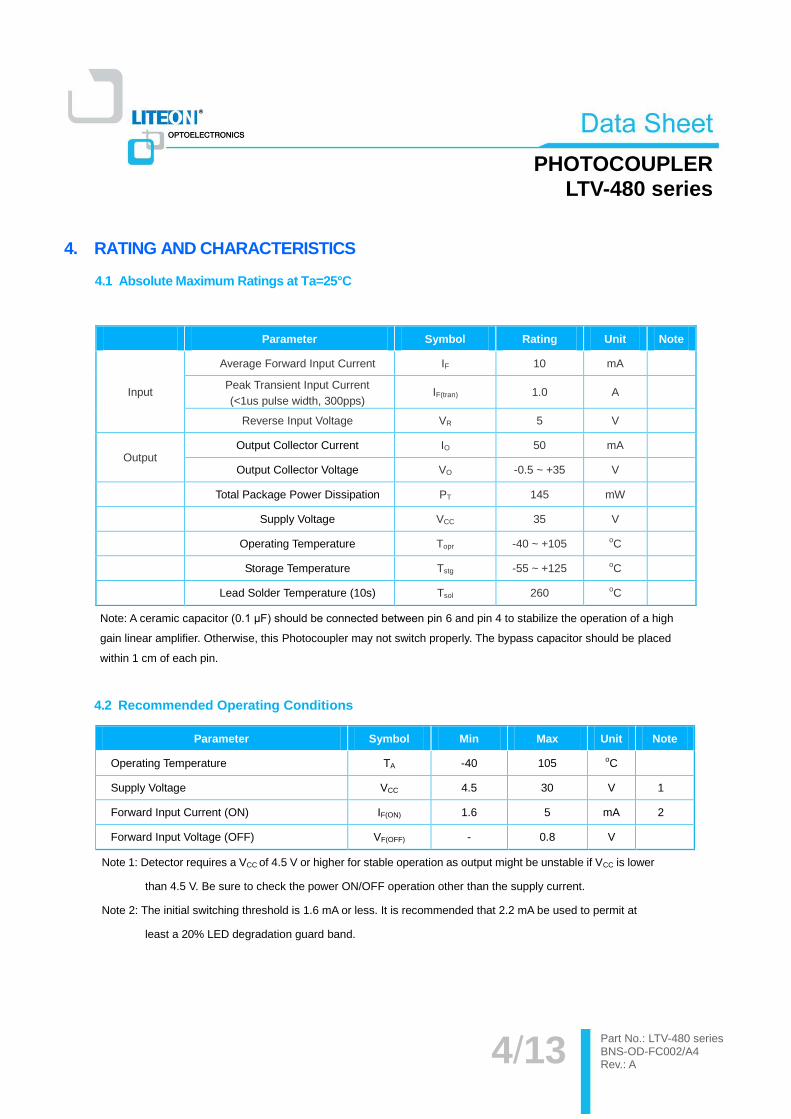
4.1 Absolute Maximum Ratings at Ta=25°C
Parameter Symbol Rating Unit Note
Input
Average Forward Input Current IF 10 mA
Peak Transient Input Current
(<1us pulse width, 300pps) IF(tran) 1.0 A
Reverse Input Voltage VR 5 V
Output Output Collector Current IO 50 mA
Output Collector Voltage VO -0.5 ~ +35 V
Total Package Power Dissipation PT 145 mW
Supply Voltage VCC 35 V
Operating Temperature Topr -40 ~ +105 oC
Storage Temperature Tstg -55 ~ +125 oC
Lead Solder Temperature (10s) Tsol 260 oC
Note: A ceramic capacitor (0.1 μF) should be connected between pin 6 and pin 4 to stabilize the operation of a high
gain linear amplifier. Otherwise, this Photocoupler may not switch properly. The bypass capacitor should be placed
within 1 cm of each pin.
4.2 Recommended Operating Conditions
Parameter Symbol Min Max Unit Note
Operating Temperature TA -40 105 oC
Supply Voltage VCC 4.5 30 V 1
Forward Input Current (ON) IF(ON) 1.6 5 mA 2
Forward Input Voltage (OFF) VF(OFF) - 0.8 V
Note 1: Detector requires a VCC of 4.5 V or higher for stable operation as output might be unstable if VCC is lower
than 4.5 V. Be sure to check the power ON/OFF operation other than the supply current.
Note 2: The initial switching threshold is 1.6 mA or less. It is recommended that 2.2 mA be used to permit at
least a 20% LED degradation guard band.
5/13
PHOTOCOUPLER
LTV-480 series
Part No.: LTV-480 series BNS-OD-FC002/A4 Rev.: A
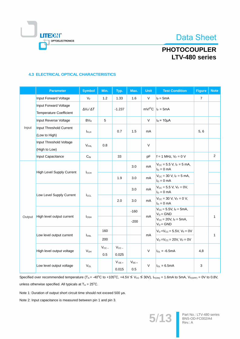
4.3 ELECTRICAL OPTICAL CHARACTERISTICS
Parameter Symbol Min. Typ. Max. Unit Test Condition Figure Note
Input
Input Forward Voltage VF 1.2 1.33 1.6 V IF = 5mA 7
Input Forward Voltage
Temperature Coefficient ΔVF/ ΔT -1.237 mV/OC IF = 5mA
Input Reverse Voltage BVR 5 V IR = 10μA
Input Threshold Current
(Low to High) IFLH 0.7 1.5 mA 5, 6
Input Threshold Voltage
(High to Low)
VFHL 0.8 V
Input Capacitance CIN 33 pF f = 1 MHz, VF = 0 V 2
Output
High Level Supply Current ICCH
3.0 mA VCC = 5.5 V, IF = 5 mA,
IO = 0 mA
1.9 3.0 mA VCC = 30 V, IF = 5 mA,
IO = 0 mA
Low Level Supply Current ICCL
3.0 mA VCC = 5.5 V, VF = 0V,
IO = 0 mA
2.0 3.0 mA VCC = 30 V, VF = 0 V,
IO = 0 mA
High level output current IOSH
-160
mA
VCC = 5.5V, IF = 5mA,
VO = GND 1
-200 VCC = 20V, IF = 5mA,
VO = GND
Low level output current IOSL
160
mA
VO =VCC = 5.5V, VF = 0V
1
200 VO =VCC = 20V, VF = 0V
High level output voltage VOH VCC –
0.5
VCC –
0.025 V IOL = -6.5mA 4,8
Low level output voltage VOL V EE +
0.015
VEE +
0.5 V IOL = 6.5mA 3
Specified over recommended temperature (TA = -40oC to +105oC, +4.5V ≤ VCC ≤ 30V), IF(ON) = 1.6mA to 5mA, VF(OFF) = 0V to 0.8V,
unless otherwise specified. All typicals at TA = 25oC.
Note 1: Duration of output short circuit time should not exceed 500 μs.
Note 2: Input capacitance is measured between pin 1 and pin 3.

6/13
PHOTOCOUPLER
LTV-480 series
Part No.: LTV-480 series BNS-OD-FC002/A4 Rev.: A
5. SWITCHING SPECIFICATION
Parameter Symbol Min. Typ. Max. Unit Test Condition Figure Note
Propagation Delay Time to
High Output Level tPLH 130 220
ns
CL = 100pF,
VF = 0V→ IF(ON) = 1.6mA
1, 9, 10,
11
1
Propagation Delay Time to
Low Output Level tPHL 120 200
CL = 100pF,
IF(ON) = 1.6mA→VF = 0V 1
Pulse Width Distortion PWD 120 CL = 100pF, 2
Propagation delay difference
between any two parts or
channels
PDD -210 210 CL = 100pF, 3
Output Rise Time (10 to 90%) Tr 35
1
Output Fall Time (90 to 10%) Tf 35
Common mode transient
immunity at high level output |CMH| 20 kV/μs
TA = 25°C,
IF = 4.0 mA,
VCM = 1500 V,
VCC = 5 V
2 4
Common mode transient
immunity at low level output |CML| 20 kV/μs
TA = 25°C,
VF = 0 V,
VCM = 1500 V,
VCC = 5 V
Over recommended operating conditions TA = -40° C to 105° C, VCC = +4.5 V to 30 V, IF(ON) = 1.6 mA to 5 mA, VF(OFF) = 0 V to 0.8 V,
unless otherwise specified. All typicals at TA = 25° C.
Note 1: The tPLH propagation delay is measured from the 50% point on the leading edge of the input pulse to the 1.3 V point on the
leading edge of the output pulse. The tPHL propagation delay is measured from the 50% point on the trailing edge of the
input pulse to the 1.3 V point on the trailing edge of the output pulse.
Note 2: Pulse Width Distortion (PWD) is defined as |tPHL - tPLH | for any given device.
Note 3: The difference of tPLH and tPHL between any two devices under the same test condition.
Note 4: CMH is the maximum slew rate of the common mode voltage that can be sustained with the output voltage in the logic high
state, VO > 2.0 V. CML is the maximum slew rate of the common mode voltage that can be sustained with the output
voltage in the logic low state, VO < 0.8 V. Note: Equal value split resistors (Rin/2) must be used at both ends of the LED.

7/13
PHOTOCOUPLER
LTV-480 series
Part No.: LTV-480 series BNS-OD-FC002/A4 Rev.: A
6. ISOLATION CHARACTERISTIC
Parameter Symbol Min. Typ. Max. Unit Test Condition Note
Withstand Insulation Test
Voltage VISO 5000 — — VRMS
RH ≤ 50%, t = 1min,
TA = 25oC 1, 2
Input-Output Resistance RI-O — 1012 — Ω VI-O = 500V DC 1
Input-Output Capacitance CI-O — 1.0 — p
F
f = 1MHz, TA = 25oC 1
Specified over recommended temperature (TA = -40oC to +105oC) unless otherwise specified. Typical values applies to TA = 25o
Note 1: Device considered a two-terminal device: pins 1, 2 and 3 shorted together and pins 4, 5 and 6 shorted together.
Note 2: In accordance with UL 1577, each optocoupler is proof tested by applying an insulation test voltage ≥ 6000 VRMS for one
second (leakage detection current limit, II-O < = 10 μA). This test is performed before the 100% production test.

8/13
PHOTOCOUPLER
LTV-480 series
Part No.: LTV-480 series BNS-OD-FC002/A4 Rev.: A
7. TEST CIRCUIT
SHIELD
VCC
C2
=1
2p
F
5kΩ
D1
D2
D3
D4
Output monitoring
node5V
Pulse Gentr = tf = 5nsf =100 kHZ
10% DUTY CYCLE
Vo=5V
Zo=50
R1 C1=120pF
Input monitoring node
619Ω
*
VOH
50%
1.3VVOL
LH HLtp tp
IF
VO
0mA
I (ON)F
Anode
Cathode
V
Vo
GND
DD1 6
5
3 4
Pulse GenV
Vo
CC1 6
5
3 4
I F
0.1μF
CL
V
Vo
CC1 6
2 5
3 4
I F
0.1μF
Pulse Gen Z=50Ω
SHIELD
SHIELD
2
tr = tf = 5nsf =100 kHZ
10% DUTY CYCLE
Vo=5V
Zo=50
2
SHIELD
VOH
50%
1.3VVOL
LH HLtp tp
IF
VO
0mA
I (ON)F
Figure 1 : tr, tf, tPLH and tPHL Test Circuit and Waveforms
Anode
Cathode
V
Vo
GND
DD1 6
5
3 4
Pulse GenV
Vo
CC1 6
5
3 4
I F
0.1μF
CL
V
Vo
CC1 6
2 5
3 4
I F
0.1μF
Pulse Gen Z=50Ω
SHIELD
SHIELD
2
tr = tf = 5nsf =100 kHZ
10% DUTY CYCLE
Vo=5V
Zo=50
2
SHIELD
VCM (PEAK)
VO(MIN.)
0V
VCM
VOH
VO(MAX)
SWITCH AT A: IF=6mA
SWITCH AT B: VF=0V
VOL
OUTPUT VO
Figure 2 : CMR Test Circuit and Waveforms

9/13
PHOTOCOUPLER
LTV-480 series
Part No.: LTV-480 series BNS-OD-FC002/A4 Rev.: A
8. TYPICAL PERFORMANCE CURVES
0
0.005
0.01
0.015
0.02
0.025
-40 -10 20 50 80 110
VO
L-
Ou
tpu
t L
ow
Vo
ltag
e -
V
TA - Temperature - oC
VF = 0 VVCC = 4.5 V
IO = 3.5mA
IO = 6.5mA
0
0.005
0.01
0.015
0.02
0.025
0.03
0.035
0.04
-40 -10 20 50 80 110
(VO
H-V
CC)
-H
igh
Ou
tpu
t V
olt
ag
e D
rop
-V
TA - Temperature - oC
IF = 4 mA
IO = 3.5mA
IO = 6.5mA
Figure 3: VOL vs. Temperature Figure 4: VOH - VCC vs. Temperature
0
1
2
3
4
5
0 0.5 1 1.5 2
VO
-O
utp
ut
Vo
ltag
e -
V
IFLH - Low To High Current Threshold - mA
IFHL
IFLH
TA = 25 oCVCC = 4.5 V
0
0.2
0.4
0.6
0.8
1
1.2
-40 -10 20 50 80 110
I F-
Inp
ut
Cu
rre
nt
-m
A
TA - Temperature - oC
VCC = 4.5 V
IFHL
IFLH
Figure 5: IFLH Hysteresis Figure 6: IFLH vs. Temperature
0. 1
1
10
10 0
1. 2 1 . 25 1. 3 1 . 35 1. 4 1 . 45 1. 5 1 . 55 1. 6
I F-
Fo
rwa
rd C
urr
en
t -
mA
VF - F o r w a rd Vo l t a ge - V
TA = 25 oC
0
5
10
15
20
25
30
35
0 5 10 15 20 25 30 35
VO
-O
ut
pu
t V
ol
ta
ge
-
V
VCC - S u p p l y V o l t a g e - V
Figure 7: Input Current vs. Forward Voltage Figure 8: Input Current vs. Forward Voltage

10/13
PHOTOCOUPLER
LTV-480 series
Part No.: LTV-480 series BNS-OD-FC002/A4 Rev.: A
60
80
100
120
140
160
180
200
-40 -10 20 50 80 110
TP
-P
rop
ag
ati
on
De
lay -
ns
TA - Temperature - oC
VCC = 4.5 V
TPHL (IF = 1.6mA)
TPHL (IF = 5mA)
TPLH (IF = 5mA)
TPLH (IF = 1.6mA)
60
80
100
120
140
160
180
200
-40 -10 20 50 80 110
TP
-P
rop
ag
ati
on
De
lay -
ns
TA - Temperature - oC
VCC = 30 V
TPHL (IF = 1.6mA)
TPHL (IF = 5mA)
TPLH (IF = 5mA)
TPLH (IF = 1.6mA)
Figure 9: Propagation Delays vs. Temperature Figure 10: Propagation Delays vs. Temperature
50
75
100
125
150
175
200
0 5 10 15 20 25 30 35
TP
-P
rop
ag
ati
on
De
lay -
ns
VCC - Supply Voltage - V
TA = 25 oC
TPHL (IF = 1.6mA)
TPHL (IF = 5mA)
TPLH (IF = 1.6mA)
TPLH (IF = 5mA)
Figure 11: Propagation Delays vs. VCC

11/13
PHOTOCOUPLER
LTV-480 series
Part No.: LTV-480 series BNS-OD-FC002/A4 Rev.: A
9. TEMPERATURE PROFILE OF SOLDERING
9.1 IR Reflow soldering (JEDEC-STD-020C compliant)
One time soldering reflow is recommended within the condition of temperature and time profile shown below. Do not solder more than three
times.
Profile item Conditions
Preheat
- Temperature Min (TSmin)
- Temperature Max (TSmax)
- Time (min to max) (ts)
150˚C
200˚C
90±30 sec
Soldering zone
- Temperature (TL)
- Time (tL)
217˚C
60 ~ 100sec
Peak Temperature (TP) 260˚C
Ramp-up rate 3˚C / sec max.
Ramp-down rate 3~6˚C / sec
60 ~ 120 sec
25 C
150 C
200 C
260 C
217 C
60-100 sec
Time (sec)
Tem
pera
ture
( C
)
20 sec
Tsmax
ts (Preheat)
tL (Soldering)
Tsmin
TL
TP
Ramp-down
Ramp-up
12/13
PHOTOCOUPLER
LTV-480 series
Part No.: LTV-480 series BNS-OD-FC002/A4 Rev.: A
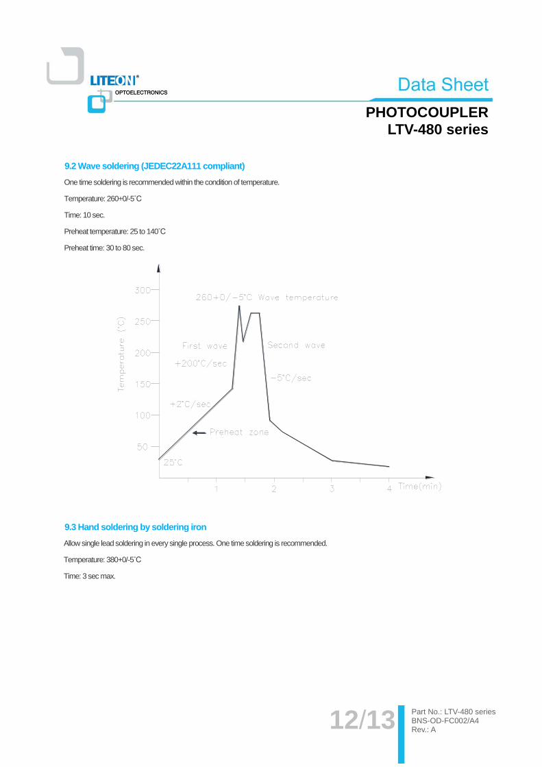
9.2 Wave soldering (JEDEC22A111 compliant)
One time soldering is recommended within the condition of temperature.
Temperature: 260+0/-5˚C
Time: 10 sec.
Preheat temperature: 25 to 140˚C
Preheat time: 30 to 80 sec.
9.3 Hand soldering by soldering iron
Allow single lead soldering in every single process. One time soldering is recommended.
Temperature: 380+0/-5˚C
Time: 3 sec max.

13/13
PHOTOCOUPLER
LTV-480 series
Part No.: LTV-480 series BNS-OD-FC002/A4 Rev.: A
10. NAMING RULE
Definition of Suffix Remark
"480" LiteOn model name
"P" clearance distance 7mm typical
"W" clearance distance 8mm typical
"TA" Pin 1 location at lower right of the tape
"TA1" Pin 1 location at upper left of the tape
"V" VDE approved option
11. Notes:
LiteOn is continually improving the quality, reliability, function or design and LiteOn reserves the right to make changes
without further notices.
The products shown in this publication are designed for the general use in electronic applications such as office automation
equipment, communications devices, audio/visual equipment, electrical application and instrumentation.
For equipment/devices where high reliability or safety is required, such as space applications, nuclear power control
equipment, medical equipment, etc, please contact our sales representatives.
When requiring a device for any ‖specific‖ application, please contact our sales in advice.
If there are any questions about the contents of this publication, please contact us at your convenience.
The contents described herein are subject to change without prior notice.
Immerge unit’s body in solder paste is not recommended.
Part Number Options
LTV-480P-TA
LTV-480P-TA1
LTV-480W-TA
LTV-480W-TA1
LTV480PTA-V
LTV480PTA1-V
LTV480WTA-V
LTV480WTA1-V