ltspice tutorial part 2- components and basic interface
TRANSCRIPT

LTspice Tutorial Part 2- Components and Basic Interface

Prerequisites
● Please make sure you have completed the following:
○ LTspice tutorial part 1 (download and installation)
Note: This guide is intended for Windows platforms. If you are using
Mac OS, please refer to Prerequisites in LTspice Tutorial Part 1-
Download and Installation for a video link on running LTspice or on
how to access Windows based EWS machines remotely.

Tutorial 2 Objectives
1. Learn the basic layout of LTspice (version XVII)
2. Be able to create circuit schematics, adjust component values,
and run basic simulations
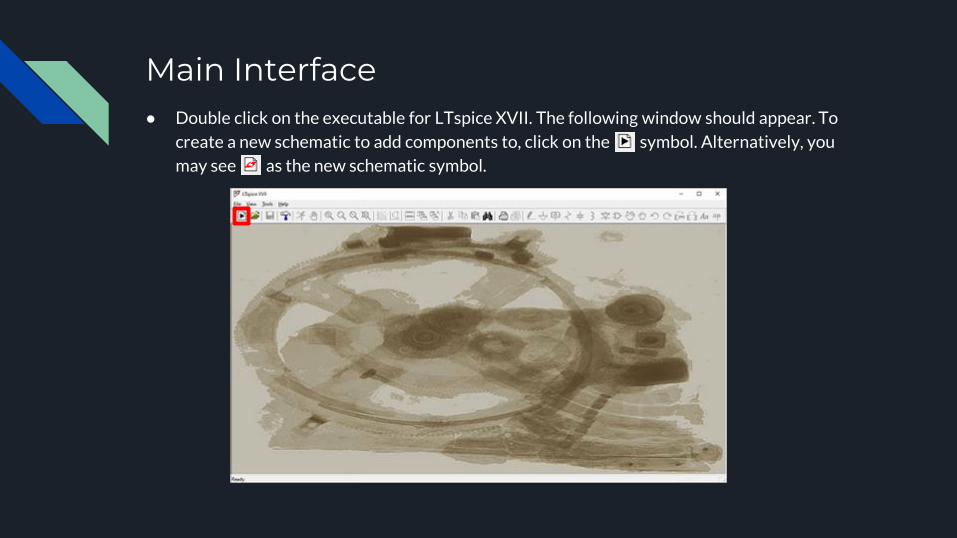
● Double click on the executable for LTspice XVII. The following window should appear. To
create a new schematic to add components to, click on the symbol. Alternatively, you
may see as the new schematic symbol.
Main Interface

● After creating a new schematic, some of the main icons will be colored. The schematic can
be saved as a .asc file. Begin by creating an empty draft.
Main Interface

Main Interface● Below are some useful icons on the interface. Once clicked, press right click or Esc to exit.
Use the mouse wheel or the microscope/zoom icons to zoom in or out.
Icon Description
Run simulation. Prior to running, simulation parameters must be specified through
Simulate > Edit Simulation Cmd.
Create new schematic (.asc file).
Establish wires or nodal connections. Continuously left click to add straight lines and establish
“wire” connections. Right click to end.
Add ground point.
Label node or point in circuit. Useful in place of wire connections in complex circuits, and for
plotting.

Main Interface● Below are some useful icons on the interface. Once clicked, press right click or Esc to exit.
Use the mouse wheel or the microscope/zoom icons to zoom in or out.
Icon Description
Add resistor.
Add capacitor.
Add inductor.
Add diode.
Add custom component, e.g. voltage source, transistors, ICs, etc.
Delete component. Left click on component to remove, or left click and drag to delete whole
portions.

Components – Basic● Adding components
○ Components such as resistors and capacitors can be added by clicking on the appropriate icon
(for shortcuts, see the list after clicking on the Edit tab).
○ Once clicked, hover to the area you wish to place the component.
○ Left click to place the component.
● Component properties○ Right click on the component to modify its properties.
○ “k”, “m”, “u”, “n”, etc. can be used as multiplication factors
e.g. “10k” on resistor = 10 kΩ, “10u” on capacitor = 10 μF
Suffix (case insensitive) PowerT 1012
G 109
Meg 106
k 103
m 10-3
u 10-6
n 10-9
p 10-12
f 10-15

Components – Basic● Moving components
○ To move a component, click on then left click on a component to move it. Click and drag to
select an entire area. Alternatively use by clicking and dragging. Can be used to move
components out of nodes, and drags the node or “wires” along with the components.
○ To rotate or mirror a component, ensure it is selected by using (initially when placing a
component it is automatically selected). Press CTRL+R to rotate the component if selected,
CTRL+E to mirror the component.
● Deleting components○ Press Delete or click on , and left click on component to delete it, or click and drag to delete an
area.
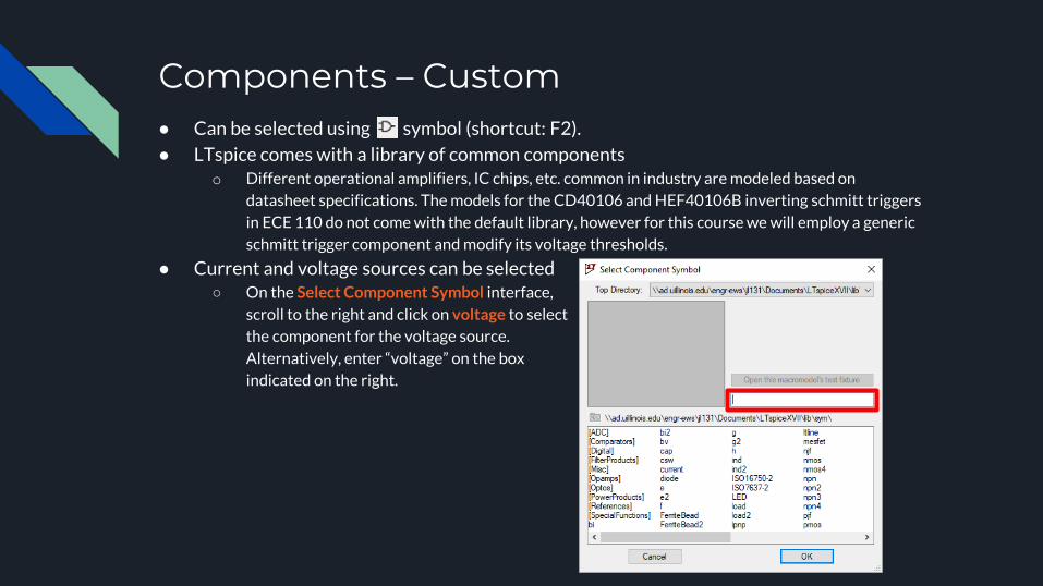
Components – Custom● Can be selected using symbol (shortcut: F2).
● LTspice comes with a library of common componentso Different operational amplifiers, IC chips, etc. common in industry are modeled based on
datasheet specifications. The models for the CD40106 and HEF40106B inverting schmitt triggers
in ECE 110 do not come with the default library, however for this course we will employ a generic
schmitt trigger component and modify its voltage thresholds.
● Current and voltage sources can be selected○ On the Select Component Symbol interface,
scroll to the right and click on voltage to select
the component for the voltage source.
Alternatively, enter “voltage” on the box
indicated on the right.
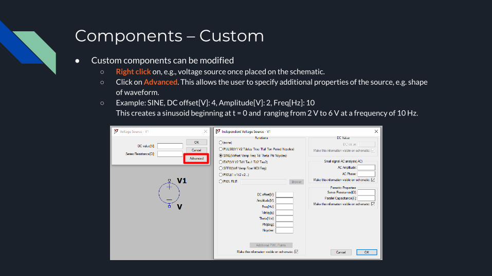
Components – Custom● Custom components can be modified
○ Right click on, e.g., voltage source once placed on the schematic.
○ Click on Advanced. This allows the user to specify additional properties of the source, e.g. shape
of waveform.
○ Example: SINE, DC offset[V]: 4, Amplitude[V]: 2, Freq[Hz]: 10
This creates a sinusoid beginning at t = 0 and ranging from 2 V to 6 V at a frequency of 10 Hz.

Net Labels● Net labels are very useful when there are many nodal connections
in your circuit. Can be selected using the symbol.
● Once clicked, the Net Name window pops up. Any name can be
chosen for a nodal point.
● Similar to the existing ground symbol , net labels establish nodal
connections for all lines connected to the symbol with that specified
name.
● Also useful when running simulation and creating plots; net labels
appear in plots.
● Example: Two “N1” net labels are placed on the diagram to the right.
Although no “wires” are drawn connecting the voltage source
and resistor, they are connected via the “N1” net label.
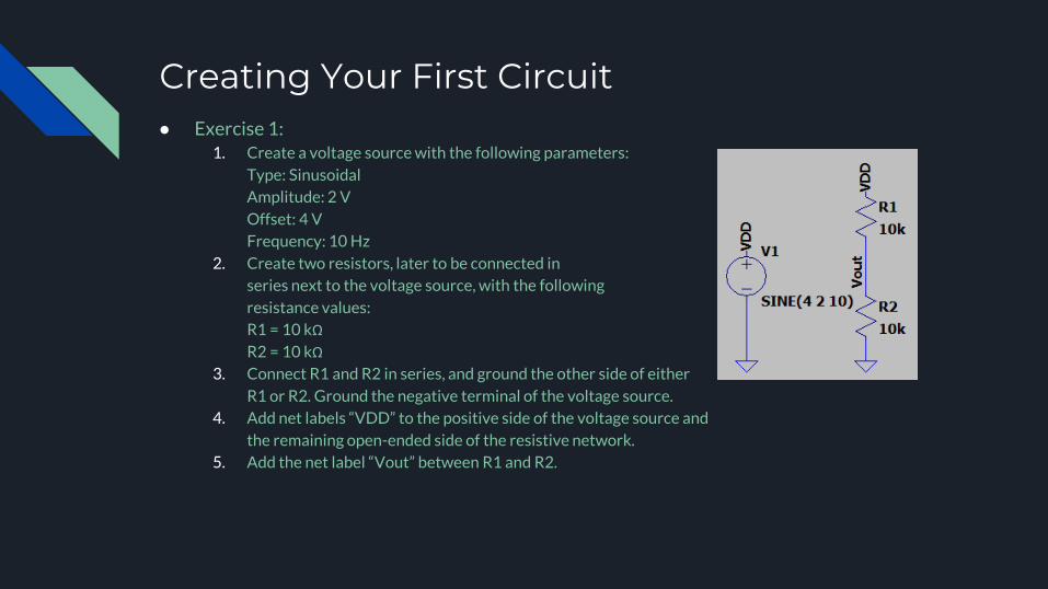
Creating Your First Circuit● Exercise 1:
1. Create a voltage source with the following parameters:
Type: Sinusoidal
Amplitude: 2 V
Offset: 4 V
Frequency: 10 Hz
2. Create two resistors, later to be connected in
series next to the voltage source, with the following
resistance values:
R1 = 10 kΩ
R2 = 10 kΩ
3. Connect R1 and R2 in series, and ground the other side of either
R1 or R2. Ground the negative terminal of the voltage source.
4. Add net labels “VDD” to the positive side of the voltage source and
the remaining open-ended side of the resistive network.
5. Add the net label “Vout” between R1 and R2.

Simulation● FIRST STEP: Once we have a basic circuit, click on
Simulate > Edit Simulation Cmd.○ The options in the Transient tab should suffice for
simulating circuit behavior for the ECE 110 course.
○ AC Analysis, DC sweep, etc. are more advanced
features that you may look up on.
○ Under Stop time, set an appropriate time based
on frequencies in your circuit. The stop time is
by default in units of seconds.
○ Click Ok and place the “.tran…” label anywhere
on your schematic.
● SECOND STEP: Click on to run the simulation.○ Empty graph should appear.
○ Click on nodal point or wire to probe it.
● Once component values are updated, or extra
components are added, the simulation needs
to be run again by clicking on , provided that the first step is complete.
Simulation● Graphing features/commands
○ Left click a node or wire to graph the voltage at that point.
○ Left click on a component to graph the current flowing through that component.
○ Hold CTRL and left click on another location to append the waveform on the graph.
○ Double left click on a point to only display that point on the graph.
○ Right click on axis values to adjust scaling.
○ Right click on the graph to adjust display settings.
○ Right click on the name of a waveform above the graph to edit the waveform, e.g. delete the
waveform or change the color.

Simulating Your Circuit● Exercise 2:
1. Using the circuit from the previous exercise, go to Simulate > Edit Simulation Cmd and set the
transient stop time to “1” (for 1 second). Click Ok and place the “.tran …” label on the schematic.
2. Run the simulation by clicking on .
3. Left click on the node containing the
“VDD” net label on your schematic.
A sinusoidal voltage waveform
should appear on the graph.
4. Hold CTRL and left click on the node
containing the “Vout” net label. Another
sinusoidal waveform should be
appended to the graph.
5. Right click on the vertical axis and
set the following parameters to
scale the axis:
Top: 6V
Tick: 1V
Bottom: 0V
6. Right click on the graph, click on View,
and tick the Grid box.
Simulating Your Circuit● Exercise 2:
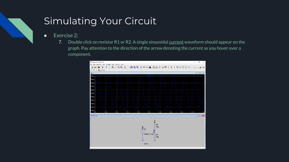
7. Double click on resistor R1 or R2. A single sinusoidal current waveform should appear on the
graph. Pay attention to the direction of the arrow denoting the current as you hover over a
component.

Saving File● Click on File > Save or Save As to begin saving your schematic (.asc file).
● Select an appropriate name and location for the file and click Save.
● To open the saved file, click on File > Open and locate the file.