ltc4012-3 - high efficiency, multi-chemistry battery ... · high efficiency, multi-chemistry...
TRANSCRIPT

�40123fb
LTC4012-3
Typical applicaTion
FeaTures
applicaTions
DescripTion
High Efficiency, Multi-Chemistry Battery Charger
with PowerPath Control
The LTC®4012-3 is a constant-current/constant-voltage battery charger controller. It uses a synchronous quasi-constant frequency PWM control architecture that will not generate audible noise with ceramic bulk capacitors. Charge current is set by external resistors and can be monitored as an output voltage across the programming resistor. With no built-in termination, the LTC4012-3 charges a wide range of batteries under external control.
The LTC4012-3 features fully adjustable output voltage. For charge management and safety, the IC includes an input P-channel MOSFET ideal diode controller, battery (output) overvoltage protection, reverse charge current protection, PWM soft-start and robust non-overlap control for an all N-channel MOSFET PWM power stage.
The device includes AC adapter input current limiting, which maximizes the charge rate for a fixed input power level. An external sense resistor programs the input current limit, and the ICL status pin indicates reduced charge current as a result of AC adapter current limiting. Ideal diode control at the adaptor input improves charger efficiency.
The CHRG status pin is active during all charging modes, including special indication for low charge current.
n General Purpose Battery Charger Controllern Efficient 550kHz Synchronous Buck PWM Topologyn ±0.5% Output Float Voltage Accuracyn Programmable Charge Current: 4% Accuracyn Programmable AC Adapter Current Limit: 3% Accuracyn No Audible Noise with Ceramic Capacitorsn INFET Low Loss Ideal Diode PowerPath™ Controln Wide Input Voltage Range: 6V to 28Vn Wide Output Voltage Range: 2V to 28Vn Indicator Outputs for Charging, C/10 Current
Detection and Input Current Limitingn Analog Charge Current Monitorn Micropower Shutdownn 20-Pin 4mm × 4mm × 0.75mm QFN Package
n Notebook Computersn Portable Instrumentsn Battery Backup Systems
Efficiency at DCIN = 20V
CLP
FROMADAPTER
13V TO 20V 0.1µF5.1k
25mΩ
3.01k
0.1µF
6.8µH
20µF
33mΩ
INFET
0.1µF
2µF
0.1µF
6.04k
26.7k
LTC4012-3
DCIN
CHRG
ICL
SHDN
ITH
PROG
CLNBOOST
TGATE
SWINTVDD
BGATETO/FROM
MCU
GND
CSP
CSN
BATFBDIV
VFB
20µF
POWER TOSYSTEM
4.7nF
32.8k
4012-3 TA01
12.3VLi-IonBATTERY
3.01k
301k +
CHARGE CURRENT (A)0
70
EFFI
CIEN
CY (%
)
POWER LOSS (m
W)
75
80
85
90
100
100
1000
10000
0.5 1 1.5 2
4012-3 TA02
2.5 3
95
LTC4012LTC4012-3
GND
X
ACPX
PIN 5 NAME
VOUT = 12.3VRSENSE = 33mΩRIN = 3.01kRPROG = 26.7k
EFFICIENCY
POWER LOSS
PART
L, LT, LTC, LTM, Linear Technology and the Linear logo are registered trademarks and PowerPath and ThinSOT are trademarks of Linear Technology Corporation. All other trademarks are the property of their respective owners. Protected by U.S. Patents including 5723970.
�40123fb
LTC4012-3
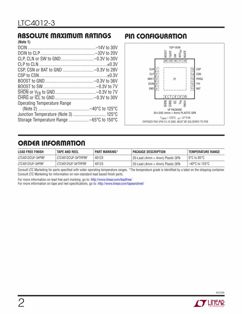
pin conFiguraTionabsoluTe MaxiMuM raTings
DCIN ............................................................–14V to 30VDCIN to CLP ................................................ –32V to 20VCLP, CLN or SW to GND ............................. –0.3V to 30VCLP to CLN ............................................................±0.3VCSP, CSN or BAT to GND ........................... –0.3V to 28VCSP to CSN ............................................................±0.3VBOOST to GND ........................................... –0.3V to 36VBOOST to SW............................................... –0.3V to 7VSHDN or VFB to GND .................................... –0.3V to 7VCHRG or ICL to GND .................................. –0.3V to 30VOperating Temperature Range
(Note 2) ............................................. –40°C to 125°CJunction Temperature (Note 3) ............................. 125°CStorage Temperature Range ..................–65°C to 150°C
(Note 1)
20 19 18 17 16
6 7 8
TOP VIEW
21
UF PACKAGE20-LEAD (4mm 4mm) PLASTIC QFN
9 10
5
4
3
2
1
11
12
13
14
15CLN
CLP
INFET
DCIN
GND
CSP
CSN
PROG
ITH
BAT
BOOS
T
TGAT
E
SW INTV
DD
BGAT
E
SHDN
CHRG ICL
V FB
FBDI
V
TJMAX = 125°C, JA = 37°C/W
EXPOSED PAD (PIN 21) IS GND, MUST BE SOLDERED TO PCB
orDer inForMaTionLEAD FREE FINISH TAPE AND REEL PART MARKING* PACKAGE DESCRIPTION TEMPERATURE RANGE
LTC4012CUF-3#PBF LTC4012CUF-3#TRPBF 40123 20-Lead (4mm × 4mm) Plastic QFN 0°C to 85°C
LTC4012IUF-3#PBF LTC4012IUF-3#TRPBF 40123 20-Lead (4mm × 4mm) Plastic QFN –40°C to 125°C
Consult LTC Marketing for parts specified with wider operating temperature ranges. *The temperature grade is identified by a label on the shipping container. Consult LTC Marketing for information on non-standard lead based finish parts.For more information on lead free part marking, go to: http://www.linear.com/leadfree/ For more information on tape and reel specifications, go to: http://www.linear.com/tapeandreel/

�40123fb
LTC4012-3
SYMBOL PARAMETER CONDITIONS MIN TYP MAX UNITS
Charge Voltage Regulation
VTOL VBAT Accuracy (See Test Circuits) C-Grade I-Grade
l
l
–0.5 –0.8 –1.0
0.5 0.8 1.0
% % %
IVFB VFB Input Bias Current VFB = 1.2V ±20 nA
RON FBDIV On Resistance ILOAD = 100µA l 85 190 ΩILEAK-FBDIV FBDIV Output Leakage Current SHDN = 0V, FBDIV = 0V l –1 0 1 µA
VBOV VFB Overvoltage Threshold l 1.235 1.281 1.32 V
Charge Current Regulation
ITOL Charge Current Accuracy with RIN = 3.01k, 6V < BAT < 18V
RPROG = 26.7k C-Grade I-Grade
l
l
–4 –5
–9.5
4 5
9.5
% % %
VSENSE = 0mV, PROG = 1.2V –12.75 –11.67 –10.95 µA
AI Current Sense Amplifier Gain (PROG ∆I) with RIN = 3.01k, 6V < BAT < 18V
VSENSE Step from 0mV to 5mV, PROG = 1.2V
–1.78 –1.66 –1.54 µA
VCS-MAX Maximum Peak Current Sense Threshold Voltage per Cycle (RIN = 3.01k)
ITH = 2V, C-Grade ITH = 2V, I-Grade ITH = 5V
l
l
l
140 125
195
325
250 265 430
mV mV mV
VC10 C/10 Indicator Threshold Voltage PROG Falling 340 400 460 mV
VREV Reverse Current Threshold Voltage PROG Falling 180 253 295 mV
Input Current Regulation
VCL Current Limit Threshold CLP – CLN C-Grade I-Grade
l
l
97 96 92
100 100
103 104 108
mV mV mV
ICLN CLN Input Bias Current CLN = CLP ±100 nA
VICL ICL Indicator Threshold (CLP – CLN) – VCL –8 –5 –2 mV
CLP Supply
OVR Operating Voltage Range 6 28 V
VUVLO CLP Undervoltage Lockout Threshold CLP Increasing l 4.65 4.85 5.25 V
VUV(HYST) UVLO Threshold Hysteresis 200 mV
ICLPO CLP Operating Current CLP = 20V, No Gate Loads 2 3 mA
Shutdown
VIL SHDN Input Voltage Low l 300 mV
VIH SHDN Input Voltage High l 1.4 V
RIN SHDN Pull-Down Resistance 40 kΩICLPS CLP Shutdown Current CLP = 12V, DCIN = 0V
SHDN = 0Vl 15
35026
500µA µA
ILEAK-BAT BAT Leakage Current SHDN = 0V or DCIN = 0V, 0V ≤ CSP = CSN = BAT ≤ 18V
l –1.5 0 1.5 µA
ILEAK-CSN CSN Leakage Current SHDN = 0V or DCIN = 0V, 0V ≤ CSP = CSN = BAT ≤ 20V
l –1.5 0 1.5 µA
ILEAK-CSP CSP Leakage Current SHDN = 0V or DCIN = 0V, 0V ≤ CSP = CSN = BAT ≤ 20V
l –1.5 0 1.5 µA
ILEAK-SW SW Leakage Current SHDN = 0V or DCIN = 0V, 0V ≤ SW ≤ 20V
l –1 0 2 µA
elecTrical characTerisTics The l denotes the specifications which apply over the full operating temperature range, otherwise specifications are at TA = 25°C. DCIN = 20V, BAT = 12V, GND = 0V unless otherwise noted. (Note 2)

�40123fb
LTC4012-3
elecTrical characTerisTics The l denotes the specifications which apply over the full operating temperature range, otherwise specifications are at TA = 25°C. DCIN = 20V, BAT = 12V, GND = 0V unless otherwise noted. (Note 2)SYMBOL PARAMETER CONDITIONS MIN TYP MAX UNITS
INTVDD Regulator
INTVDD Output Voltage No Load l 4.85 5 5.15 V
∆VDD Load Regulation IDD = 20mA –0.4 –1 %
IDD Short-Circuit Current (Note 5) INTVDD = 0V 50 85 130 mA
Switching Regulator
VACP AC Present Charge Enable Threshold Voltage DCIN – BAT, DCIN Rising C-Grade I-Grade
l
l
350 300
500
650 700
mV mV
IITH ITH Current ITH = 1.4V –40/+90 µA
fTYP Typical Switching Frequency 467 550 633 kHz
fMIN Minimum Switching Frequency CLOAD = 3.3nF 20 25 kHz
DCMAX Maximum Duty Cycle CLOAD = 3.3nF 98 99 %
tR-TG TGATE Rise Time CLOAD = 3.3nF, 10% – 90% 60 110 ns
tF-TG TGATE Fall Time CLOAD = 3.3nF, 90% – 10% 50 110 ns
tR-BG BGATE Rise Time CLOAD = 3.3nF, 10% – 90% 60 110 ns
tF-BG BGATE Fall Time CLOAD = 3.3nF, 90% – 10% 60 110 ns
tNO TGATE, BGATE Non-Overlap Time CLOAD = 3.3nF, 10% – 10% 110 ns
PowerPath Control
IDCIN DCIN Input Current 0V ≤ DCIN ≤ CLP l –10 60 µA
VFTO Forward Turn-On Voltage (DCIN Detection Threshold) DCIN-CLP, DCIN Rising l 15 60 mV
VFR Forward Regulation Voltage DCIN-CLP l 15 25 35 mV
VRTO Reverse Turn-Off Voltage DCIN-CLP, DCIN Falling l –45 –25 –15 mV
VOL(INFET) INFET Output Low Voltage, Relative to CLP DCIN-CLP = 0.1V, IINFET =1µA –6.5 –5 V
VOH(INFET) INFET Output High Voltage, Relative to CLP DCIN-CLP = –0.1V, IINFET =–5µA –250 250 mV
tIF(ON) INFET Turn-On Time To CLP-INFET > 3V, CINFET = 1nF 85 180 µs
tIF(OFF) INFET Turn-Off Time To CLP-INFET < 1.5V, CINFET = 1nF 2.5 6 µs
Indicator Outputs
VOL Output Voltage Low ILOAD = 100µA, PROG = 1.2V 500 mV
ILEAK Output Leakage SHDN = 0V, DCIN = 0V, VOUT = 20V l –10 10 µA
IC10 CHRG C/10 Current Sink CHRG = 2.5V l 15 25 38 µA
Note 1: Stresses beyond those listed under Absolute Maximum Ratings may cause permanent damage to the device. Exposure to any Absolute Maximum Rating condition for extended periods may affect device reliability and lifetime.Note 2: The LTC4012C-3 is guaranteed to meet performance specifications over the 0°C to 85°C operating temperature range. The LTC4012I-3 is guaranteed to meet performance specifications over the –40°C to 125°C operating temperature range.
Note 3: Operating junction temperature TJ (in °C) is calculated from the ambient temperature TA and the total continuous package power dissipation PD (in watts) by the formula TJ = TA + (θJA • PD). Refer to the Applications Information section for details.Note 4: All currents into device pins are positive; all currents out of device pins are negative. All voltages are referenced to GND, unless otherwise specified.Note 5: Output current may be limited by internal power dissipation. Refer to the Applications Information section for details.
�40123fb
LTC4012-3
Battery Load Dump
BATT
ERY
VOLT
AGE
(500
mV/
DIV)
LOADSTATE
TIME (1ms/DIV)CLP = 20VVOUT = 12.3V
4012-3 G06
DISCONNECT
RECONNECT
3A
2A
12.1V 1A1A
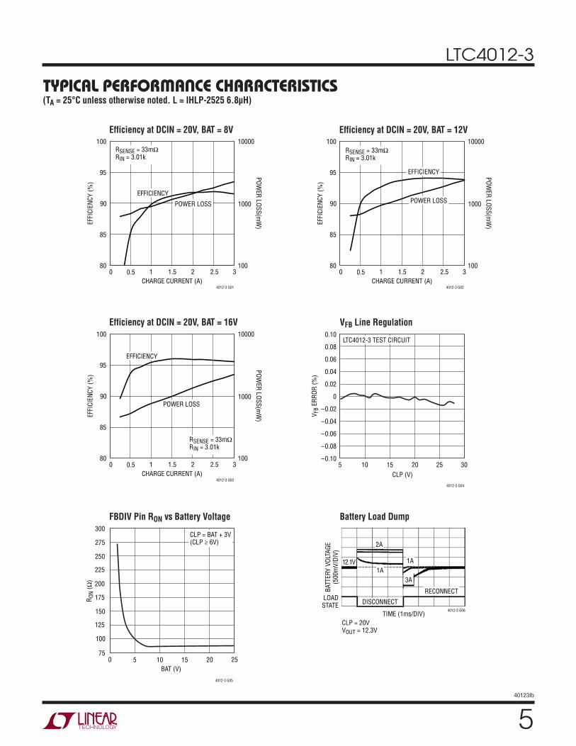
Typical perForMance characTerisTics
Efficiency at DCIN = 20V, BAT = 8V
VFB Line Regulation
CHARGE CURRENT (A)0
80
EFFI
CIEN
CY (%
)
POWER LOSS(m
W)
85
90
100
100
1000
10000
0.5 1 1.5 2
4012-3 G01
2.5 3
95
POWER LOSS
EFFICIENCY
RSENSE = 33mΩRIN = 3.01k
Efficiency at DCIN = 20V, BAT = 12V
CHARGE CURRENT (A)0
80
EFFI
CIEN
CY (%
)
POWER LOSS(m
W)
85
90
100
100
1000
10000
0.5 1 1.5 2
4012-3 G02
2.5 3
95 EFFICIENCY
POWER LOSS
RSENSE = 33mΩRIN = 3.01k
Efficiency at DCIN = 20V, BAT = 16V
CHARGE CURRENT (A)0
80
EFFI
CIEN
CY (%
)
POWER LOSS(m
W)
85
90
100
100
1000
10000
0.5 1 1.5 2
4012-3 G03
2.5 3
95EFFICIENCY
POWER LOSS
RSENSE = 33mΩRIN = 3.01k
CLP (V)5
V FB
ERRO
R (%
)
0.02
0.06
0.10
25
4012-3 G04
–0.02
–0.06
0
0.04
0.08
–0.04
–0.08
–0.1010 15 20 30
LTC4012-3 TEST CIRCUIT
BAT (V)0
75
R ON
(Ω)
100
150
175
200
10 20 25
300
4012-3 G05
125
5 15
225
250
275CLP = BAT + 3V(CLP ≥ 6V)
FBDIV Pin RON vs Battery Voltage
(TA = 25°C unless otherwise noted. L = IHLP-2525 6.8µH)
�40123fb
LTC4012-3
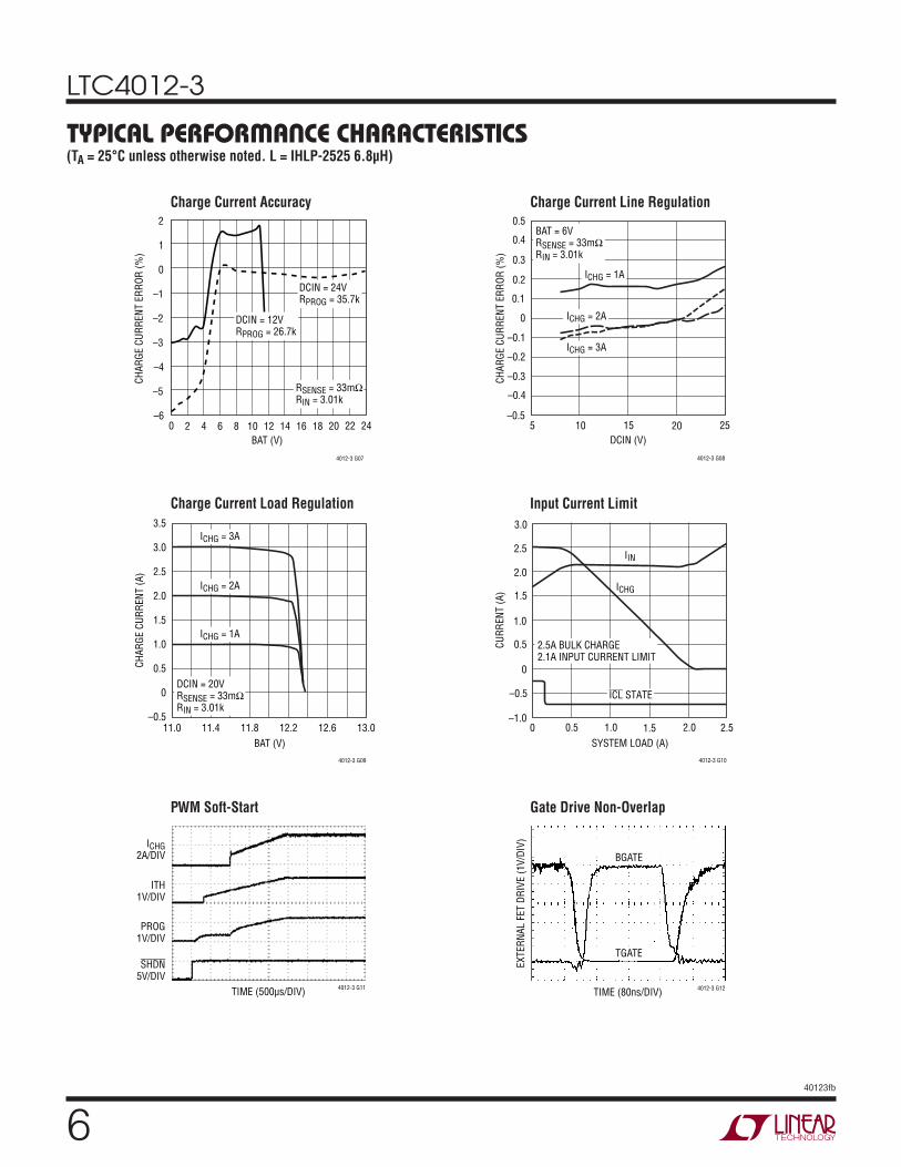
Gate Drive Non-Overlap
Charge Current Line Regulation
Input Current Limit
DCIN (V)5
–0.5
CHAR
GE C
URRE
NT E
RROR
(%)
–0.4
–0.2
–0.1
0
0.5
0.2
10 15
4012-3 G08
–0.3
0.3
0.4
0.1
20 25
ICHG = 1A
ICHG = 2A
ICHG = 3A
BAT = 6VRSENSE = 33mΩRIN = 3.01k
Charge Current Load Regulation
BAT (V)11.0
CHAR
GE C
URRE
NT (A
)
3.5
3.0
2.5
2.0
1.5
1.0
0.5
0
–0.512.6
4012-3 G09
11.4 11.8 12.2 13.0
ICHG = 3A
ICHG = 2A
ICHG = 1A
DCIN = 20VRSENSE = 33mΩRIN = 3.01k
SYSTEM LOAD (A)0
CURR
ENT
(A)
0.5
1.0
1.5
1.5 2.5
4012-3 G10
0
–0.5
–1.00.5 1.0 2.0
2.0
2.5
3.0
IIN
ICHG
ICL STATE
2.5A BULK CHARGE2.1A INPUT CURRENT LIMIT
PWM Soft-Start
ICHG2A/DIV
TIME (500µs/DIV) 4012-3 G11
ITH1V/DIV
PROG1V/DIV
SHDN5V/DIV
TIME (80ns/DIV)
EXTE
RNAL
FET
DRI
VE (1
V/DI
V)
4012-3 G12
TGATE
BGATE
Typical perForMance characTerisTics(TA = 25°C unless otherwise noted. L = IHLP-2525 6.8µH)
Charge Current Accuracy
BAT (V)0
–6
CHAR
GE C
URRE
NT E
RROR
(%)
–4
–3
–2
108 20 2422
2
4012-3 G07
–5
642 1412 16 18
–1
0
1
DCIN = 12VRPROG = 26.7k
DCIN = 24VRPROG = 35.7k
RSENSE = 33mΩRIN = 3.01k
�40123fb
LTC4012-3
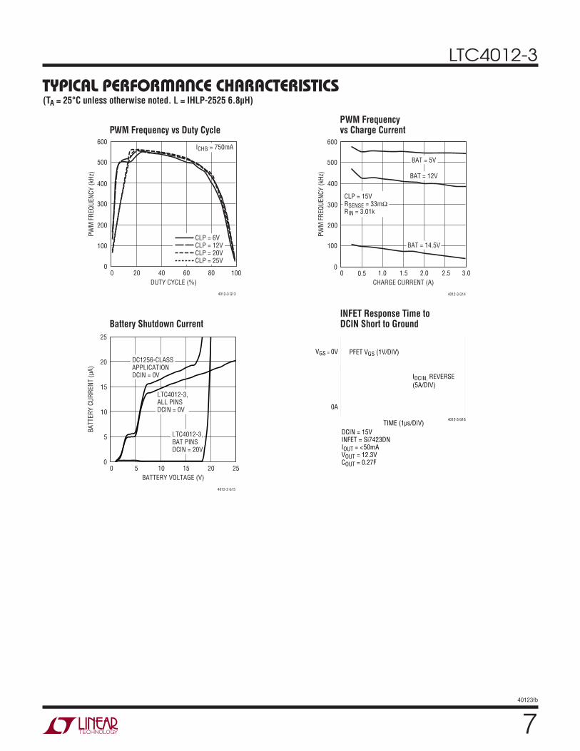
Typical perForMance characTerisTics
PWM Frequency vs Duty Cycle
Battery Shutdown Current
DUTY CYCLE (%)0
0
PWM
FRE
QUEN
CY (k
Hz)
100
200
300
400
500
600
20 40 60 80
4012-3 G13
100
CLP = 6VCLP = 12VCLP = 20VCLP = 25V
ICHG = 750mA
PWM Frequency vs Charge Current
CHARGE CURRENT (A)0
0
PWM
FRE
QUEN
CY (k
Hz)
100
200
300
400
600
0.5 1.0 1.5 2.0
4012-3 G14
2.5 3.0
500
BAT = 14.5V
BAT = 12V
BAT = 5V
CLP = 15VRSENSE = 33mΩRIN = 3.01k
BATTERY VOLTAGE (V)0
0
BATT
ERY
CURR
ENT
(µA)
5
10
15
25
5 10 15
4012-3 G15
20 25
20
LTC4012-3,BAT PINSDCIN = 20V
LTC4012-3,ALL PINSDCIN = 0V
DC1256-CLASSAPPLICATIONDCIN = 0V
(TA = 25°C unless otherwise noted. L = IHLP-2525 6.8µH)
INFET Response Time to DCIN Short to Ground
0A
VGS = 0V
TIME (1µs/DIV)DCIN = 15VINFET = Si7423DNIOUT = <50mAVOUT = 12.3VCOUT = 0.27F
4012-3 G16
PFET VGS (1V/DIV)
IDCIN, REVERSE(5A/DIV)

�40123fb
LTC4012-3
pin FuncTionsCLN (Pin 1): Adapter Input Current Limit Negative Input. The LTC4012-3 senses voltage on this pin to determine if less charge current should be sourced to limit total input current. The threshold is set 100mV below the CLP pin. An external filter should be used to remove switching noise. This input should be tied to CLP if not used. Operating voltage range is (CLP – 110mV) to CLP.
CLP (Pin 2): Adapter Input Current Limit Positive Input. The LTC4012-3 also draws power from this pin, including a small amount for some shutdown functions. Operating voltage range is GND to 28V.
INFET (Pin 3): PowerPath Control Output. This output drives the gate of a PMOS pass transistor connected between the DC input (DCIN) and the raw system supply rail (CLP) to maintain a forward voltage of 25mV when a DC input source is present. INFET is internally clamped about 6V below CLP. Maximum operating voltage is CLP, which is used to turn off the input PMOS transistor when the DC input is removed.
DCIN (Pin 4): DC Sense Input. One of two voltage sense inputs to the internal PowerPath controller (the other input to the controller is CLP). This input is usually supplied from an input DC power source. Operating voltage ranges from GND to 28.2V.
GND (Pin 5): Ground. Internally connected to the Exposed Pad (package paddle).
SHDN (Pin 6): Active-Low Shutdown Input. Driving SHDN below 300mV unconditionally forces the LTC4012-3 into the shutdown state. This input has a 40kΩ internal pull-down to GND. Operating voltage range is GND to INTVDD.
CHRG (Pin 7): Active-Low Charge Indicator Output. This open-drain output provides three levels of information about charge status using a strong pull-down, 25µA weak pull-down or high impedance. Refer to the Operation and Applications Information sections for further details. This output should be left floating if not used.
ICL (Pin 8): Active-Low Input Current Limit Indicator Out-put. This open-drain output pulls to GND when the charge current is reduced because of AC adapter input current limiting. This output should be left floating if not used.
VFB (Pin 9): Battery Voltage Feedback Input. An external resistor divider between FBDIV and GND with the center tap connected to VFB programs the charger output voltage. In constant voltage mode, this pin is nominally at 1.2085V. Refer to the Applications Information section for complete details on programming battery voltage. Operating voltage range is GND to 1.25V.
FBDIV (Pin 10): Battery Voltage Feedback Resistor Divider Source. The LTC4012-3 connects this pin to BAT when charging is in progress. FBDIV is an open-drain PFET output to BAT with an operating voltage range of GND to BAT.
BAT (Pin 11): Battery Pack Connection. The LTC4012-3 uses the voltage on this pin to control PWM operation when charging. Operating voltage range is GND to CLN.
ITH (Pin 12): PWM Control Voltage and Compensation Node. The LTC4012-3 develops a voltage on this pin to control cycle-by-cycle peak inductor current. An external R-C network connected to ITH provides PWM loop com-pensation. Refer to the Applications Information section for further details on establishing loop stability. Operating voltage range is GND to INTVDD.
PROG (Pin 13): Charge Current Programming and Monitor-ing Pin. An external resistance connected between PROG and GND, along with the current sense and PWM input resistors, programs the maximum charge current. The voltage on this pin can also provide a linearized indicator of charge current. Refer to the Applications Information section for complete details on current programming and monitoring. Operating voltage range is GND to INTVDD.
CSN (Pin 14): Charge Current Sense Negative Input. Place an external input resistor (RIN, Figure 1) between this pin and the negative side of the charge current sense resistor. Operating voltage ranges from (BAT – 50mV) to (BAT + 200mV).
CSP (Pin 15): Charge Current Sense Positive Input. Place an external input resistor (RIN, Figure 1) between this pin and the positive side of the charge current sense resistor. Operating voltage ranges from (BAT – 50mV) to (BAT + 200mV).
�40123fb
LTC4012-3
pin FuncTionsBGATE (Pin 16): External Synchronous NFET Gate Control Output. This output provides gate drive to an external NMOS power transistor switch used for synchronous rectification to increase efficiency in the step-down DC/DC converter. Operating voltage is GND to INTVDD. BGATE should be left floating if not used.
INTVDD (Pin 17): Internal 5V Regulator Output. This pin provides a means of bypassing the internal 5V regulator used to power the LTC4012-3 PWM FET drivers. This sup-ply shuts down when the LTC4012-3 shuts down. Refer to the Application Information section for details if additional power is drawn from this pin by the application circuit.
SW (Pin 18): PWM Switch Node. The LTC4012-3 uses the voltage on this pin as the source reference for its topside NFET (PWM switch) driver. Refer to the Applications In-formation section for additional PCB layout suggestions related to this critical circuit node. Operating voltage range is GND to CLN.
TGATE (Pin 19): External NFET Switch Gate Control Output. This output provides gate drive to an external NMOS power transistor switch used in the DC/DC converter. Operating voltage range is GND to (CLN + 5V).
BOOST (Pin 20): TGATE Driver Supply Input. A bootstrap capacitor is returned to this pin from a charge network connected to SW and INTVDD. Refer to the Applications Information section for complete details on circuit topol-ogy and component values. Operating voltage ranges from (INTVDD – 1V) to (CLN + 5V).
GND (Exposed Pad Pin 21): Ground. The package paddle provides a single-point ground for the internal voltage reference and other critical LTC4012-3 circuits. It should be soldered to a suitable PCB copper ground pad for proper electrical operation and to obtain the specified package thermal resistance.

�040123fb
LTC4012-3
block DiagraM
–––+
–
+
19
EA
R1
TO INTERNALCIRCUITS
TOINTERNALCIRCUITS
CC
–
+CA
1.2085VREFERENCE
5VREGULATOR
PWMLOGIC
FAULTDETECTION
C/10DETECTION
SHUTDOWNCONTROL
OSCILLATORBAT
SHUTDOWN
CHARGE
INPUTCURRENT
LIMIT
TGATE
20BOOST
12ITH
13PROG
14CSN
15CSP
18SW
21
GND(PADDLE)
4012-3 BD01
16BGATE
17INTVDD
TOINTERNALCIRCIUTS
11
VFB9
CHRG
ACP
7
FBDIV10
GND
6SHDN
ICL8
CLP
CLN
2
1
INFET3
DCIN4
+
–IF
5
��40123fb
LTC4012-3
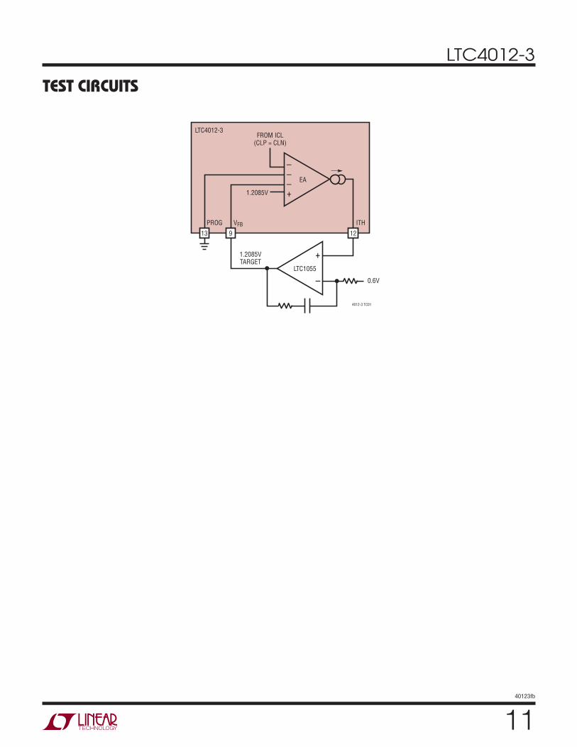
TesT circuiTs
–––+
913 12
1.2085V
1.2085VTARGET
PROG VFB ITH
4012-3 TC01
LTC4012-3
0.6V
EA
FROM ICL(CLP = CLN)
–
+LTC1055

��40123fb
LTC4012-3
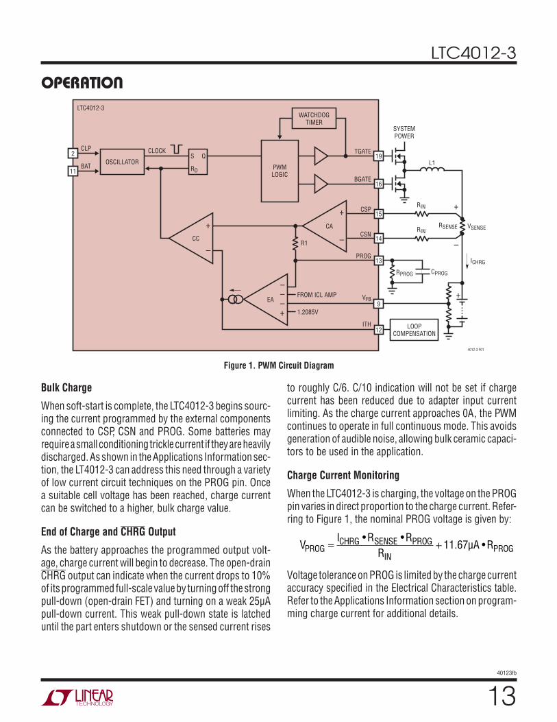
operaTionOverview
The LTC4012-3 is a synchronous step-down (buck) cur-rent mode PWM battery charger controller. The maximum charge current is programmed by the combination of a charge current sense resistor (RSENSE), matched input resistors (RIN, Figure 1), and a programming resistor (RPROG) between the PROG and GND pins. Battery voltage is programmed with an external resistor divider between FBDIV and GND. In addition, the PROG pin provides a linearized voltage output of the actual charge current.
The LTC4012-3 does not have built-in charge termination and is flexible enough for charging any type of battery chemistry. It is a building block IC intended for use with an external circuit, such as a microcontroller, capable of managing the entire algorithm required for the specific battery being charged. The LTC4012-3 features a shut-down input and various state indicator outputs, allowing easy and direct management by a wide range of external (digital) charge controllers.
Shutdown
The LTC4012-3 remains in shutdown until DCIN is greater than 5.1V and exceeds CLP by 60mV and SHDN is driven above 1.4V. In shutdown, current drain from the battery is reduced to the lowest possible level, thereby increasing standby time. When in shutdown, the ITH pin is pulled to GND and CHRG, ICL, FET gate drivers and INTVDD are all disabled. Charging can be stopped at any time by forcing SHDN below 300mV.
AC Present Detection
AC present is detected as soon as DCIN exceeds BAT by at least 500mV. Charging is not enabled until this condition is first met. After this event, charging is no longer gated by AC present detection. If battery voltage rises due to ESR, or DCIN droops due to current load, the PWM will remain enabled, even with very low input overhead, unless DCIN falls below the supply voltage on CLP.
Input PowerPath Control
The input PFET controller performs many important func-tions. First, it monitors DCIN and enables the charger when this input voltage is higher than the raw CLP sys-tem supply. Next, it controls the gate of an external input power PFET to maintain a low forward voltage drop when charging, creating improved efficiency. It also prevents reverse current flow through this same PFET, providing a suitable input blocking function. Finally, it helps avoid synchronous boost operation during invalid operating conditions by detecting elevated CLP voltage and forcing the charger off.
If DCIN voltage is less than CLP, then DCIN must rise 60mV higher than CLP to enable the charger and activate the ideal diode control. The gate of the input PFET is driven to a voltage sufficient to regulate a forward drop between DCIN and CLP of about 25mV. If the input voltage differential drops below this point, the FET is turned off slowly. If the voltage between DCIN and CLP drops to less than –25mV, the input FET is turned off in less than 6µs to prevent significant reverse current from flowing back through the PFET, and the charger is disabled.
Soft-Start
Exiting the shutdown state enables the charger and releases the ITH pin. When enabled, switching will not begin until DCIN exceeds BAT by 500mV and ITH exceeds a threshold that assures initial current will be positive (about 5% to 25% of the maximum programmed current). To limit inrush current, soft-start delay is created with the compensation values used on the ITH pin. Longer soft-start times can be realized by increasing the filter capacitor on ITH, if reduced loop bandwidth is acceptable. The actual charge current at the end of soft-start will depend on which loop (current, voltage or adapter limit) is in control of the PWM. If this current is below that required by the ITH start-up threshold, the resulting charge current transient duration depends on loop compensation but is typically less than 100µs.
��40123fb
LTC4012-3
Bulk Charge
When soft-start is complete, the LTC4012-3 begins sourc-ing the current programmed by the external components connected to CSP, CSN and PROG. Some batteries may require a small conditioning trickle current if they are heavily discharged. As shown in the Applications Information sec-tion, the LT4012-3 can address this need through a variety of low current circuit techniques on the PROG pin. Once a suitable cell voltage has been reached, charge current can be switched to a higher, bulk charge value.
End of Charge and CHRG Output
As the battery approaches the programmed output volt-age, charge current will begin to decrease. The open-drain CHRG output can indicate when the current drops to 10% of its programmed full-scale value by turning off the strong pull-down (open-drain FET) and turning on a weak 25µA pull-down current. This weak pull-down state is latched until the part enters shutdown or the sensed current rises
to roughly C/6. C/10 indication will not be set if charge current has been reduced due to adapter input current limiting. As the charge current approaches 0A, the PWM continues to operate in full continuous mode. This avoids generation of audible noise, allowing bulk ceramic capaci-tors to be used in the application.
Charge Current Monitoring
When the LTC4012-3 is charging, the voltage on the PROG pin varies in direct proportion to the charge current. Refer-ring to Figure 1, the nominal PROG voltage is given by:
V
I R RR
µA RPROGCHRG SENSE PROG
INPROG= +
• •. •11 67
Voltage tolerance on PROG is limited by the charge current accuracy specified in the Electrical Characteristics table. Refer to the Applications Information section on program-ming charge current for additional details.
operaTion
Figure 1. PWM Circuit Diagram
–––+
–
+
EA
CA
–
+CC
192
11PWMLOGIC
OSCILLATOR
WATCHDOGTIMER
LOOPCOMPENSATION
TGATE
SYSTEMPOWER
L1
RIN +
–
16BGATE
15CSP
14CSN
13PROG
9VFB
12ITH
RPROG
R1
FROM ICL AMP
1.2085V
RSENSE VSENSE
ICHRG
4012-3 F01
CPROG
QSCLOCK
LTC4012-3
CLP
BAT RD
RIN
+

��40123fb
LTC4012-3
Adapter Input Current Limit
The LTC4012-3 can monitor and limit current from the input DC supply, which is normally an AC adapter. When the programmed adapter input current is reached, charge current is reduced to maintain the desired maximum input current. The ITH and PROG pins will reflect the reduced charge current. This limit function avoids overloading the DC input source, allowing the product to operate at the same time the battery is charging without complex load management algorithms. The battery will automatically be charged at the maximum possible rate that the adapter will support, given the application’s operating condition. The LTC4012-3 can only limit input current by reducing charge current, and in this case the charger uses nonsynchro-nous PWM operation to prevent boosting if the average charge current falls below about 25% of the maximum programmed current. Note that the ICL indicator output becomes active (low) at an adapter input current level just slightly less than that required for the internal amplifier to begin to assert control over the PWM loop.
Charger Status Indicator Outputs
The LTC4012-3 open-drain indicator outputs provide valu-able information about the IC’s operating state and can be used for a variety of purposes in applications. Table 1 summarizes the state of the indicator outputs as a function of LTC4012-3 operation.
operaTionTable 1. LTC4012-3 Open-Drain Indicator Outputs
CHRG ICL CHARGER STATEOff Off No DC Input (Shutdown)
or Reverse CurrentOn Off Bulk Charge
25µA Off Low Current Charge or Initial DCIN – BAT <500mV
On On Input Current Limit During Bulk Charge
25µA On Input Current Limit During Low Current Charge
PWM Controller
The LTC4012-3 uses a synchronous step-down architec-ture to produce high operating efficiency. The nominal operating frequency of 550kHz allows use of small filter components. The following conceptual discussion of basic PWM operation references Figure 1.
The voltage across the external charge current sense resistor RSENSE is measured by current amplifier, CA. This instantaneous current (VSENSE/RIN) is fed to the PROG pin where it is averaged by an external capacitor and converted to a voltage by the programming resistor RPROG between PROG and GND. The PROG voltage becomes the average charge current input signal to error amplifier, EA. EA also receives loop control information from the battery voltage feedback input, VFB, and the adapter input current limit circuit.
Figure 2. PWM Waveforms
ON
OFF
OFF
INDUCTORCURRENT
TOP FET
BOTTOM FET
ON
tOFF
THRESHOLDSET BY ITHVOLTAGE
4012-3 F02

��40123fb
LTC4012-3
The ITH output of the error amplifier is a scaled control voltage for one input of the PWM comparator, CC. ITH sets a peak inductor current threshold, sensed by R1, to maintain the desired average current through RSENSE. The current comparator output does this by switching the state of the RS latch at the appropriate time.
At the beginning of each oscillator cycle, the PWM clock sets the RS latch and turns on the external topside NFET (bottom-side synchronous NFET off) to refresh the current carried by the external inductor L1. The inductor current and voltage across RSENSE begin to rise linearly. CA buffers this instantaneous voltage rise and applies it to CC with gain supplied by R1. When the voltage across R1 exceeds the peak level set by the ITH output of EA, the top FET turns off and the bottom FET turns on. The inductor cur-rent then ramps down linearly until the next rising PWM clock edge. This closes the loop and sources the correct inductor current to maintain the desired parameter (charge current, battery voltage, or input current). To produce a near constant frequency, the PWM oscillator implements the equation:
t
CLP BATCLP kHzOFF = –
• 550
Repetitive, closed-loop waveforms for stable PWM opera-tion appear in Figure 2.
PWM Watchdog Timer
As input and output conditions vary, the LTC4012-3 may need to utilize PWM duty cycles approaching 100%. In this case, operating frequency may be reduced well below 550kHz. An internal watchdog timer observes the activity on the TGATE pin. If TGATE is on for more than 40µs, the watchdog activates and forces the bottom NFET on (top NFET off) for about 100ns. This avoids a
potential source of audible noise when using ceramic input or output capacitors and prevents the boost supply capacitor for the top gate driver from discharging. In low drop out operation, the actual charge current may not be able to reach the programmed full-scale value due to the watchdog function.
Overvoltage Protection
The LTC4012-3 also contains overvoltage detection that prevents transient battery voltage overshoots of more than about 6% above the programmed output voltage. When battery overvoltage is detected, both external MOSFETs are turned off until the overvoltage condition clears, at which time a new soft-start sequence begins. This is useful for properly charging battery packs that use an internal switch to disconnect themselves for performing functions such as calibration or pulse mode charging.
Reverse Charge Current Protection (Anti-Boost)
Because the LTC4012-3 always attempts to operate synchronously in full continuous mode (to avoid audible noise from ceramic capacitors), reverse average charge current can occur during some invalid operating condi-tions. INFET PowerPath control avoids boosting a lightly loaded system supply during reverse operation. However, under heavier system loads, CLP may not boost above DCIN, even though reverse average current is flowing. In this case a second circuit monitors indication of reverse average current on PROG.
If either of these circuits detects boost operation, The LTC4012-3 turns off both external MOSFETs until the reverse current condition clears. At that point, a new soft-start sequence begins.
operaTion

��40123fb
LTC4012-3
applicaTions inForMaTionProgramming Charge Current
The formula for charge current is:
I
RR
VR
µACHRGIN
SENSE PROG=
•.
– .1 2085
11 67
The LTC4012-3 operates best with 3.01k input resistors, although other resistors near this value can be used to accommodate standard sense resistor values. Refer to the subsequent discussion on inductor selection for other considerations that come into play when selecting input resistors RIN.
RSENSE should be chosen according to the following equation:
R
mVISENSEMAX
= 100
where IMAX is the desired maximum charge current ICHRG. The 100mV target can be adjusted to some degree to obtain standard RSENSE values and/or a desired RPROG value, but target voltages lower than 100mV will cause a proportional reduction in current regulation accuracy.
The required minimum resistance between PROG and GND can be determined by applying the suggested expression for RSENSE while solving the first equation given above for charge current with ICHRG = IMAX:
R
V RV µA RPROG MIN
IN
IN( )
. •. . •
=+
1 20850 1 11 67
If RIN is chosen to be 3.01k with a sense voltage of 100mV, this equation indicates a minimum value for RPROG of 26.9k. Table 6 gives some examples of recommended charge current programming component values based on these equations.
The resistance between PROG and GND can simply be set with a single a resistor, if only maximum charge cur-rent needs to be controlled during the desired charging algorithm.
However, some batteries require a low charge current for initial conditioning when they are heavily discharged. The charge current can then be safely switched to a higher level after conditioning is complete. Figure 3 illustrates one method of doing this with 2-level control of the PROG pin resistance. Turning Q1 off reduces the charge current to IMAX/10 for battery conditioning. When Q1 is on, the LTC4012-3 is programmed to allow full IMAX current for bulk charge. This technique can be expanded through the use of additional digital control inputs for an arbitrary number of pre-programmed current values.
For a truly continuous range of maximum charge current control, pulse width modulation can be used as shown in Figure 4.
Figure 3. Programming 2-Level Charge Current
13
Q12N7002
4012-3 F03
R253.6k
PROG
LTC4012-3
R126.7k
CPROG4.7nF
BULKCHARGE
PRECHARGE
Figure 4. Programming PWM Current
13
Q12N7002
4012-3 F04
PROG
LTC4012-3
RPROGRMAX511k
CPROG
0V
5V
��40123fb
LTC4012-3
applicaTions inForMaTionThe value of RPROG controls the maximum value of charge current which can be programmed (Q1 continuously on). PWM of the Q1 gate voltage changes the value of RPROG to produce lower currents. The frequency of this modula-tion should be higher than a few kHz, and CPROG must be increased to reduce the ripple caused by switching Q1. In addition, it may be necessary to increase loop compensa-tion capacitance connected to ITH to maintain stability or prevent large current overshoot during start-up. Selecting a higher Q1 PWM frequency (≈10kHz) will reduce the need to change CPROG or other compensation values. Charge current will be proportional to the duty cycle of the PWM input on the gate of Q1.
Programming LTC4012-3 Output Voltage
Figure 5 shows the external circuit for programming the charger output voltage. The voltage is then governed by the following equation:
VV R RR
R R A R BBAT =+( ) = +
1 2085 1 22
2 2 2. •
,
See Table 2 for approximate resistor values for R2.
R R
VR R A R B1 2
1 20851 2 2 2=
= +VBAT
.– ,
Selecting R2 to be less than 50k and the sum of R1 and R2 at least 200k or above, achieves the lowest possible error at the VFB sense input. Note that sources of error such as R1 and R2 tolerance, FBDIV RON or VFB input im-pedance are not included in the specifications given in the Electrical Characteristics. This leads to the possibility that very accurate (0.1%) external resistors might be required. Actually, the temperature rise of the LTC4012-3 will rarely exceed 50°C at the end of charge, because charge current will have tapered to a low level. This means that 0.25% resistors will normally provide the required level of overall accuracy. Table 2 gives recommended values for R1 and R2 for popular lithium-ion battery voltages. For values of R1 above 200k, addition of capacitor CZ may improve transient response and loop stability. A value of 10pF is normally adequate.
Table 2. Programming Output Voltage VBAT (V)
R1 (0.25%) (kΩ)
R2A (0.25%) (kΩ)
R2B (1%)* (Ω)
4.1 165 69 –
4.2 167 67.3 200
8.2 162 28 –
8.4 169 28.4 –
12.3 301 32.8 –
12.6 294 31.2 –
16.4 284 22.6 –
16.8 271 21 –
20.5 316 19.8 –
21 298 18.2 –
24.6 298 15.4 –
25.2 397 20 –
*To Obtain Desired Accuracy Requires Series Resistors For R2.
Figure 5. Programming Output Voltage
11
10
BAT
FBDIV
85ΩTYPICAL
9VFB
LTC4012-3 R1
R2A
R2B*
4012-3 F05
CZ
21GND
(EXPOSED PAD)
*OPTIONAL TRIM RESISTOR
+
��40123fb
LTC4012-3
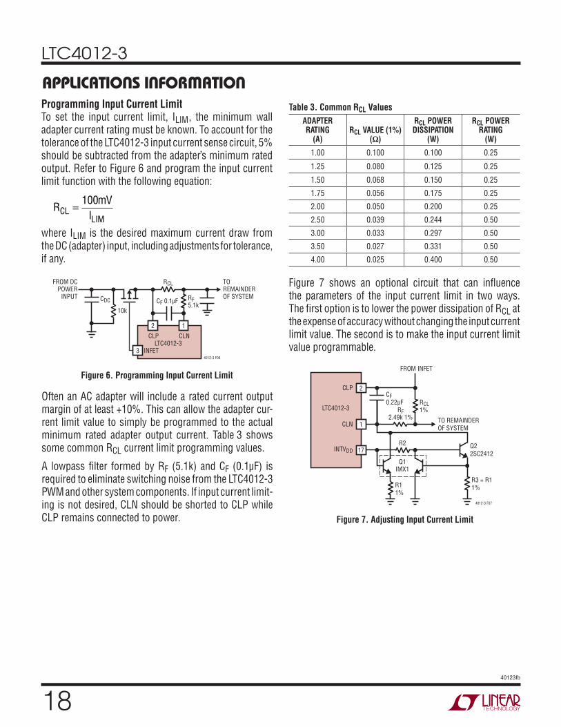
applicaTions inForMaTionProgramming Input Current LimitTo set the input current limit, ILIM, the minimum wall adapter current rating must be known. To account for the tolerance of the LTC4012-3 input current sense circuit, 5% should be subtracted from the adapter’s minimum rated output. Refer to Figure 6 and program the input current limit function with the following equation:
R
mVICLLIM
= 100
where ILIM is the desired maximum current draw from the DC (adapter) input, including adjustments for tolerance, if any.
Figure 6. Programming Input Current Limit
2 1
RCL
CDC CF 0.1µF
CLPLTC4012-3
CLN
RF5.1k
4012-3 F06
10k
FROM DCPOWER
INPUT
TOREMAINDEROF SYSTEM
3 INFET
2
1
CLP
CLN
17INTVDD
LTC4012-3RCL1%
R3 = R11%R1
1%
Q22SC2412
RF2.49k 1%
R2
Q1IMX1
4012-3 F07
CF0.22µF
TO REMAINDEROF SYSTEM
FROM INFET
Figure 7. Adjusting Input Current Limit
Table 3. Common RCL ValuesADAPTER RATING
(A)
RCL VALUE (1%)
(Ω)
RCL POWER DISSIPATION
(W)
RCL POWER RATING
(W)
1.00 0.100 0.100 0.25
1.25 0.080 0.125 0.25
1.50 0.068 0.150 0.25
1.75 0.056 0.175 0.25
2.00 0.050 0.200 0.25
2.50 0.039 0.244 0.50
3.00 0.033 0.297 0.50
3.50 0.027 0.331 0.50
4.00 0.025 0.400 0.50
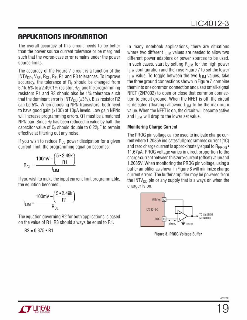
Figure 7 shows an optional circuit that can influence the parameters of the input current limit in two ways. The first option is to lower the power dissipation of RCL at the expense of accuracy without changing the input current limit value. The second is to make the input current limit value programmable.
Often an AC adapter will include a rated current output margin of at least +10%. This can allow the adapter cur-rent limit value to simply be programmed to the actual minimum rated adapter output current. Table 3 shows some common RCL current limit programming values.
A lowpass filter formed by RF (5.1k) and CF (0.1µF) is required to eliminate switching noise from the LTC4012-3 PWM and other system components. If input current limit-ing is not desired, CLN should be shorted to CLP while CLP remains connected to power.
��40123fb
LTC4012-3
applicaTions inForMaTionThe overall accuracy of this circuit needs to be better than the power source current tolerance or be margined such that the worse-case error remains under the power source limits.
The accuracy of the Figure 7 circuit is a function of the INTVDD, VBE, RCL, RF , R1 and R3 tolerances. To improve accuracy, the tolerance of RF should be changed from 5.1k, 5% to a 2.49k 1% resistor. RCL and the programming resistors R1 and R3 should also be 1% tolerance such that the dominant error is INTVDD (±3%). Bias resistor R2 can be 5%. When choosing NPN transistors, both need to have good gain (>100) at 10µA levels. Low gain NPNs will increase programming errors. Q1 must be a matched NPN pair. Since RF has been reduced in value by half, the capacitor value of CF should double to 0.22µF to remain effective at filtering out any noise.
If you wish to reduce RCL power dissipation for a given current limit, the programming equation becomes:
R
mVk
RICLLIM
=
1005 2 49
1–
• .
If you wish to make the input current limit programmable, the equation becomes:
I
mVk
RRLIM
CL=
1005 2 49
1–
• .
The equation governing R2 for both applications is based on the value of R1. R3 should always be equal to R1.
R2 = 0.875 • R1Figure 8. PROG Voltage Buffer
17
13
INTVDD
PROG
<30nA
LTC4012-3
4012-3 F08
TO SYSTEMMONITOR+
–
In many notebook applications, there are situations where two different ILIM values are needed to allow two different power adapters or power sources to be used. In such cases, start by setting RLIM for the high power ILIM configuration and then use Figure 7 to set the lower ILIM value. To toggle between the two ILIM values, take the three ground connections shown in Figure 7, combine them into one common connection and use a small-signal NFET (2N7002) to open or close that common connec-tion to circuit ground. When the NFET is off, the circuit is defeated (floating) allowing ILIM to be the maximum value. When the NFET is on, the circuit will become active and ILIM will drop to the lower set value.
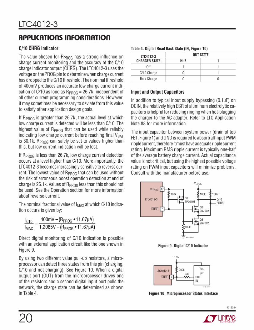
Monitoring Charge Current
The PROG pin voltage can be used to indicate charge cur-rent where 1.2085V indicates full programmed current (1C) and zero charge current is approximately equal to RPROG • 11.67µA. PROG voltage varies in direct proportion to the charge current between this zero-current (offset) value and 1.2085V. When monitoring the PROG pin voltage, using a buffer amplifier as shown in Figure 8 will minimize charge current errors. The buffer amplifier may be powered from the INTVDD pin or any supply that is always on when the charger is on.
�040123fb
LTC4012-3
applicaTions inForMaTionTable 4. Digital Read Back State (IN, Figure 10)
LTC4012-3 CHARGER STATE
OUT STATE
Hi-Z 1
Off 1 1
C/10 Charge 0 1
Bulk Charge 0 0
Input and Output Capacitors
In addition to typical input supply bypassing (0.1µF) on DCIN, the relatively high ESR of aluminum electrolytic ca-pacitors is helpful for reducing ringing when hot-plugging the charger to the AC adapter. Refer to LTC Application Note 88 for more information.
The input capacitor between system power (drain of top FET, Figure 1) and GND is required to absorb all input PWM ripple current, therefore it must have adequate ripple current rating. Maximum RMS ripple current is typically one-half of the average battery charge current. Actual capacitance value is not critical, but using the highest possible voltage rating on PWM input capacitors will minimize problems. Consult with the manufacturer before use.
Figure 10. Microprocessor Status Interface
33k200k
4012-3 F10
VDD
3.3V
µP
INOUT
LTC4012-3
CHRG 7
C/10 CHRG Indicator
The value chosen for RPROG has a strong influence on charge current monitoring and the accuracy of the C/10 charge indicator output (CHRG). The LTC4012-3 uses the voltage on the PROG pin to determine when charge current has dropped to the C/10 threshold. The nominal threshold of 400mV produces an accurate low charge current indi-cation of C/10 as long as RPROG = 26.7k, independent of all other current programming considerations. However, it may sometimes be necessary to deviate from this value to satisfy other application design goals.
If RPROG is greater than 26.7k, the actual level at which low charge current is detected will be less than C/10. The highest value of RPROG that can be used while reliably indicating low charge current before reaching final VBAT is 30.1k. RPROG can safely be set to values higher than this, but low current indication will be lost.
If RPROG is less than 26.7k, low charge current detection occurs at a level higher than C/10. More importantly, the LTC4012-3 becomes increasingly sensitive to reverse cur-rent. The lowest value of RPROG that can be used without the risk of erroneous boost operation detection at end of charge is 26.1k. Values of RPROG less than this should not be used. See the Operation section for more information about reverse current.
The nominal fractional value of IMAX at which C/10 indica-tion occurs is given by:
II
mV R µAV R
C
MAX
PROG
PROG
10 400 11 671 2085
=( )– • .
. – •• .11 67µA( )Direct digital monitoring of C/10 indication is possible with an external application circuit like the one shown in Figure 9.
By using two different value pull-up resistors, a micro-processor can detect three states from this pin (charging, C/10 and not charging). See Figure 10. When a digital output port (OUT) from the microprocessor drives one of the resistors and a second digital input port polls the network, the charge state can be determined as shown in Table 4.
Figure 9. Digital C/10 Indicator
17
7
INTVDD
CHRG
Q1TP0610T
Q22N7002
100k
LTC4012-3
4012-3 F09
100k
VLOGIC
100k
C/10CHRG
100k
Q32N7002

��40123fb
LTC4012-3
The output capacitor shown across the battery and ground must also absorb PWM output ripple current. The general formula for this capacitor current is:
I
VVV
L fRMS
BATBAT
CLP
PWM=
0 29 1
1
. • • –
•
For example, IRMS = 0.22A with:
VBAT = 12.6V VCLP = 19V L1 = 10µH fPWM = 550kHz
High capacity ceramic capacitors (20µF or more) available from a variety of manufacturers can be used for input/out-put capacitors. Other alternatives include OS-CON and POSCAP capacitors from Sanyo.
Low ESR solid tantalum capacitors have high ripple cur-rent rating in a relatively small surface mount package, but exercise caution when using tantalum for input or output bulk capacitors. High input surge current can be created when the adapter is hot-plugged to the charger or when a battery is connected to the charger. Solid tan-talum capacitors have a known failure mechanism when subjected to very high surge currents. Select tantalum capacitors that have high surge current ratings or have been surge tested.
EMI considerations usually make it desirable to minimize ripple current in battery leads. Adding Ferrite beads or inductors can increase battery impedance at the nominal 550kHz switching frequency. Switching ripple current splits between the battery and the output capacitor in inverse relation to capacitor ESR and the battery impedance. If the ESR of the output capacitor is 0.2Ω and the battery impedance is raised to 4Ω with a ferrite bead, only 5% of the current ripple will flow to the battery.
Inductor Selection
Higher switching frequency generally results in lower ef-ficiency because of MOSFET gate charge losses, but it allows smaller inductor and capacitor values to be used. A primary effect of the inductor value L1 is the amplitude of ripple current created. The inductor ripple current ∆IL decreases with higher inductance and PWM operating frequency:
∆I
V VV
L fL
BATBAT
CLP
PWM=
• –
•
1
1
Accepting larger values of ∆IL allows the use of low in-ductance, but results in higher output voltage ripple and greater core losses. Lower charge currents generally call for larger inductor values.
The LTC4012-3 limits maximum instantaneous peak in-ductor current during every PWM cycle. To avoid unstable switch waveforms, the ripple current must satisfy:
∆I mV
RIL
SENSEMAX<
2 150• –
so choose:
LV
fmV
RI
CLP
PWMSENSE
MAX
10 125
150>
. •
• –
For C-grade parts, a reasonable starting point for setting ripple current is ∆IL = 0.4 • IMAX. For I-grade parts, use ∆IL = 0.2 • IMAX only if the IC will actually be used to charge batteries over the wider I-grade temperature range. The voltage compliance of internal LTC4012-3 circuits also imposes limits on ripple current. Select RIN (in Figure 1) to avoid average current errors in high ripple designs. The following equation can be used for guidance:
R IµA
RR I
µASENSE L
INSENSE L• •∆ ∆
50 20≤ ≤
applicaTions inForMaTion
��40123fb
LTC4012-3
RIN should not be less than 2.37k or more than 6.04k. Val-ues of RIN greater than 3.01k may cause some reduction in programmed current accuracy. Use these equations and guidelines, as represented in Table 5, to help select the cor-rect inductor value. This table was developed for C-grade parts to maintain maximum ∆IL near 0.6 • IMAX with fPWM at 550kHz and VBAT = 0.5 • VCLP (the point of maximum ∆IL), assuming that inductor value could also vary by 25% at IMAX. For I-grade parts, reduce maximum ∆IL to less than 0.4 • IMAX, but only if the IC will actually be used to charge batteries over the wider I-grade temperature range. In that case, a good starting point can be found by multiplying the inductor values shown in Table 5 by a factor of 1.6 and rounding up to the nearest standard value.
Table 5. Minimum Typical Inductor Values
VCLP
L1 (Typ) IMAX RSENSE RIN RPROG
<10V ≥10µH 1A 100mΩ 3.01k 26.7k
10V to 20V ≥20µH 1A 100mΩ 3.01k 26.7k
>20V ≥28µH 1A 100mΩ 3.01k 26.7k
<10V ≥5.1µH 2A 50mΩ 3.01k 26.7k
10V to 20V ≥10µH 2A 50mΩ 3.01k 26.7k
>20V ≥14µH 2A 50mΩ 3.01k 26.7k
<10V ≥3.4µH 3A 33mΩ 3.01k 26.7k
10V to 20V ≥6.8µH 3A 33mΩ 3.01k 26.7k
>20V ≥9.5µH 3A 33mΩ 3.01k 26.7k
<10V ≥2.5µH 4A 25mΩ 3.01k 26.7k
10V to 20V ≥5.1µH 4A 25mΩ 3.01k 26.7k
>20V ≥7.1µH 4A 25mΩ 3.01k 26.7k
To guarantee that a chosen inductor is optimized in any given application, use the design equations provided and perform bench evaluation in the target application, par-ticularly at duty cycles below 20% or above 80% where PWM frequency can be much less than the nominal value of 550kHz.
TGATE BOOST Supply
Use the external components shown in Figure 11 to develop a bootstrapped BOOST supply for the TGATE FET driver. A good set of equations governing selection of the two capacitors is:
C
QV
C CG120
4 52 20 1= =
•.
, •
where QG is the rated gate charge of the top external NFET with VGS = 4.5V. The maximum average diode current is then given by:
ID = QG • 665kHz
To improve efficiency by increasing VGS applied to the top FET, substitute a Schottky diode with low reverse leakage for D1.
PWM jitter has been observed in some designs operating at higher VIN/VOUT ratios. This jitter does not substantially affect DC charge current accuracy. A series resistor with a value of 5Ω to 20Ω can be inserted between the cathode of D1 and the BOOST pin to remove this jitter, if present. A resistor case size of 0603 or larger is recommended to lower ESL and achieve the best results.
applicaTions inForMaTion
Figure 11. TGATE Boost Supply
20
17
BOOST
INTVDD
18SW
LTC4012-3
4012-3 F11
C22µF
C10.1µF
L1TORSENSE
D11N4148
��40123fb
LTC4012-3
applicaTions inForMaTionFET Selection
Two external power MOSFETs must be selected for use with the charger: an N-channel power switch (top FET) and an N-channel synchronous rectifier (bottom FET). Peak gate-to-source drive levels are internally set to about 5V. Consequently, logic-level FETs must be used. In addition to the fundamental DC current, selection criteria for these MOSFETs also include channel resis-tance RDS(ON), total gate charge QG, reverse transfer capacitance CRSS, maximum rated drain-source voltage BVDSS and switching characteristics such as td(ON/OFF). Power dissipation for each external FET is given by:
PV I T R
V
k V
D TOPBAT MAX DS ON
CLP
C
( )( )• •
•
=+( )
+
2 1 δ∆
LLP MAX RSS
D BOTCLP BAT M
I C kHz
PV V I
2 665• • •
– •( ) = ( ) AAX DS ON
CLP
T R
V
2 1• ( )+( )δ∆
where δ is the temperature dependency of RDS(ON), ∆T is the temperature rise above the point specified in the FET data sheet for RDS(ON) and k is a constant in-versely related to the internal LTC4012-3 top gate driver. The term (1 + δ∆T) is generally given for a MOSFET in the form of a normalized RDS(ON) curve versus temperature, but δ of 0.005/°C can be used as a suitable approxima-tion for logic-level FETs if other data is not available. CRSS = ∆QGD/∆VDS is usually specified in the MOSFET characteristics. The constant k = 2 can be used in esti-mating top FET dissipation. The LTC4012-3 is designed to work best with external FET switches with a total gate charge at 5V of 15nC or less.
For VCLP < 20V, high charge current efficiency generally improves with larger FETs, while for VCLP > 20V, top gate transition losses increase rapidly to the point that using a topside NFET with higher RDS(ON) but lower CRSS can actually provide higher efficiency. If the charger will be operated with a duty cycle above 85%, overall efficiency is normally improved by using a larger top FET.
The synchronous (bottom) FET losses are greatest at high input voltage or during a short circuit, which forces a low side duty cycle of nearly 100%. Increasing the size of this FET lowers its losses but increases power dissipation in the LTC4012-3. Using asymmetrical FETs will normally achieve cost savings while allowing optimum efficiency.
Select FETs with BVDSS that exceeds the maximum VCLP voltage that will occur. Both FETs are subjected to this level of stress during operation. Many logic-level MOSFETs are limited to 30V or less.
The LTC4012-3 uses an improved adaptive TGATE and BGATE drive that is insensitive to MOSFET inertial delays, td(ON/OFF), to avoid overlap conduction losses. Switching characteristics from power MOSFET data sheets apply only to a specific test fixture, so there is no substitute for bench evaluation of external FETs in the target application. In general, MOSFETs with lower inertial delays will yield higher efficiency.
Diode Selection
A Schottky diode in parallel with the bottom FET and/or top FET in an LTC4012-3 application clamps SW during the non-overlap times between conduction of the top and bottom FET switches. This prevents the body diode of the MOSFETs from forward biasing and storing charge, which could reduce efficiency as much as 1%. One or both diodes can be omitted if the efficiency loss can be tolerated. A 1A Schottky is generally a good size for 3A chargers due to the low duty cycle of the non-overlap times. Larger diodes can actually result in additional efficiency (transition) losses due to larger junction capacitance.
Loop Compensation and Soft-Start
The three separate PWM control loops of the LTC4012-3 can be compensated by a single set of components at-tached between the ITH pin and GND. As shown in the typical LTC4012-3 application, a 6.04k resistor in series with a capacitor of at least 0.1µF provides adequate loop compensation for the majority of applications.
��40123fb
LTC4012-3
Figure 12. High Speed Switching Path
4012 F12
VBAT
L1 RSENSE
HIGHFREQUENCY
CIRCULATINGPATH BAT
ANALOGGROUND
SYSTEMGROUND
SWITCH NODE
CIN
SWITCHING GROUND
COUT
VIN
GND
D1+
The LTC4012-3 can be soft-started with the compensation capacitor on the ITH pin. At start-up, ITH will quickly rise to about 0.25V, then ramp up at a rate set by the com-pensation capacitor and the 40µA ITH bias current. The full programmed charge current will be reached when ITH reaches approximately 2V. With a 0.1µF capacitor, the time to reach full charge current is usually greater than 1.5ms. This capacitor can be increased if longer start-up times are required, but loop bandwidth and dynamic response will be reduced.
INTVDD Regulator Output
Bypass the INTVDD regulator output to GND with a low ESR X5R or X7R ceramic capacitor with a value of 0.47µF or larger. The capacitor used to build the BOOST supply (C2 in Figure 11) can serve as this bypass. Do not draw more than 30mA from this regulator for the host system, governed by IC power dissipation.
Calculating IC Power Dissipation
The user should ensure that the maximum rated junction temperature is not exceeded under all operating conditions. The thermal resistance of the LTC4012-3 package (θJA) is 37°C/W, provided the Exposed Pad is in good thermal contact with the PCB. The actual thermal resistance in the application will depend on forced air cooling and other heat sinking means, especially the amount of copper on the PCB to which the LTC4012-3 is attached. The following formula may be used to estimate the maximum aver-age power dissipation, PD (in watts), of the LTC4012-3, which is dependent upon the gate charge of the external MOSFETs. This gate charge, which is a function of both gate and drain voltage swings, is determined from speci-fications or graphs in the manufacturer’s data sheet. For the equation below, find the gate charge for each transistor assuming 5V gate swing and a drain voltage swing equal to the maximum VCLP voltage. Maximum LTC4012-3 power dissipation under normal operating conditions is then given by:
PD = DCIN(3mA + IDD + 665kHz(QTGATE + QBGATE)) – 5IDD
applicaTions inForMaTionwhere:
IDD = Average external INTVDD load current, if any
QTGATE = Gate charge of external top FET in Coulombs
QBGATE = Gate charge of external bottom FET in Coulombs
PCB Layout Conciderations
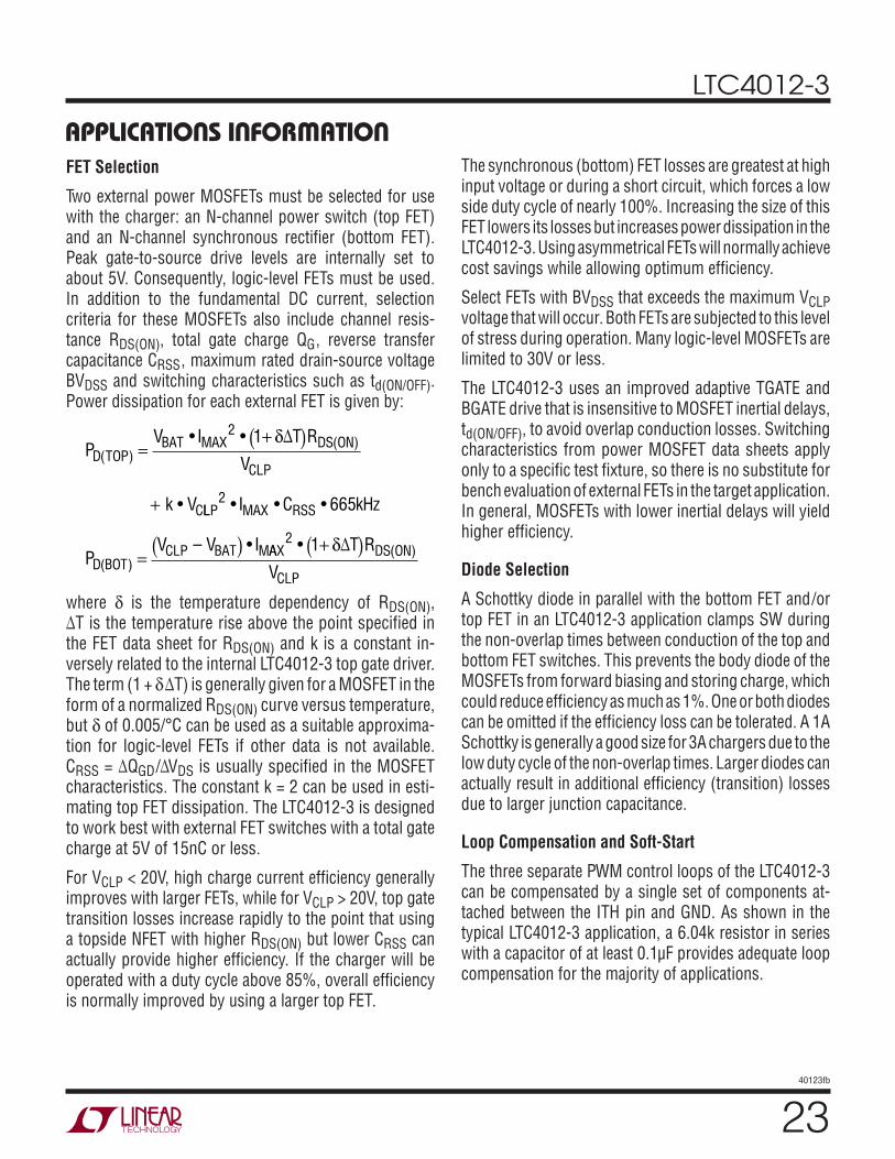
To prevent magnetic and electrical field radiation and high frequency resonant problems, proper layout of the components connected to the LTC4012-3 is essential. Refer to Figure 12. For maximum efficiency, the switch node rise and fall times should be minimized. The following PCB design priority list will help insure proper topology. Layout the PCB using this specific order.
1. Input capacitors should be placed as close as possible to switching FET supply and ground connections with the shortest copper traces possible. The switching FETs must be on the same layer of copper as the input capacitors. Vias should not be used to make these connections.
2. Place the LTC4012-3 close to the switching FET gate terminals, keeping the connecting traces short to pro-duce clean drive signals. This rule also applies to IC supply and ground pins that connect to the switching FET source pins. The IC can be placed on the opposite side of the PCB from the switching FETs.
��40123fb
LTC4012-3
3. Place the inductor input as close as possible to the switching FETs. Minimize the surface area of the switch node. Make the trace width the minimum needed to support the programmed charge current. Use no cop-per fills or pours. Avoid running the connection on multiple copper layers in parallel. Minimize capacitance from the switch node to any other trace or plane.
4. Place the charge current sense resistor immediately adjacent to the inductor output, and orient it such that current sense traces to the LTC4012-3 are not long. These feedback traces need to be run together as a single pair with the smallest spacing possible on any given layer on which they are routed. Locate any filter component on these traces next to the LTC4012-3, and not at the sense resistor location.
5. Place output capacitors adjacent to the sense resistor output and ground.
6. Output capacitor ground connections must feed into the same copper that connects to the input capacitor ground before connecting back to system ground.
7. Connection of switching ground to system ground, or any internal ground plane, should be single-point. If the system has an internal system ground plane, a good way to do this is to cluster vias into a single star point to make the connection.
8. Route analog ground as a trace tied back to the LTC4012-3 GND pin and paddle before connecting to any other ground. Avoid using the system ground plane. A useful CAD technique is to make analog ground a separate ground net and use a 0Ω resistor to connect analog ground to system ground.
9. A good rule of thumb for via count in a given high current path is to use 0.5A per via. Be consistent when applying this rule.
10. If possible, place all the parts listed above on the same PCB layer.
11. Copper fills or pours are good for all power connections except as noted above in Rule 3. Copper planes on multiple layers can also be used in parallel. This helps with thermal management and lowers trace inductance, which further improves EMI performance.
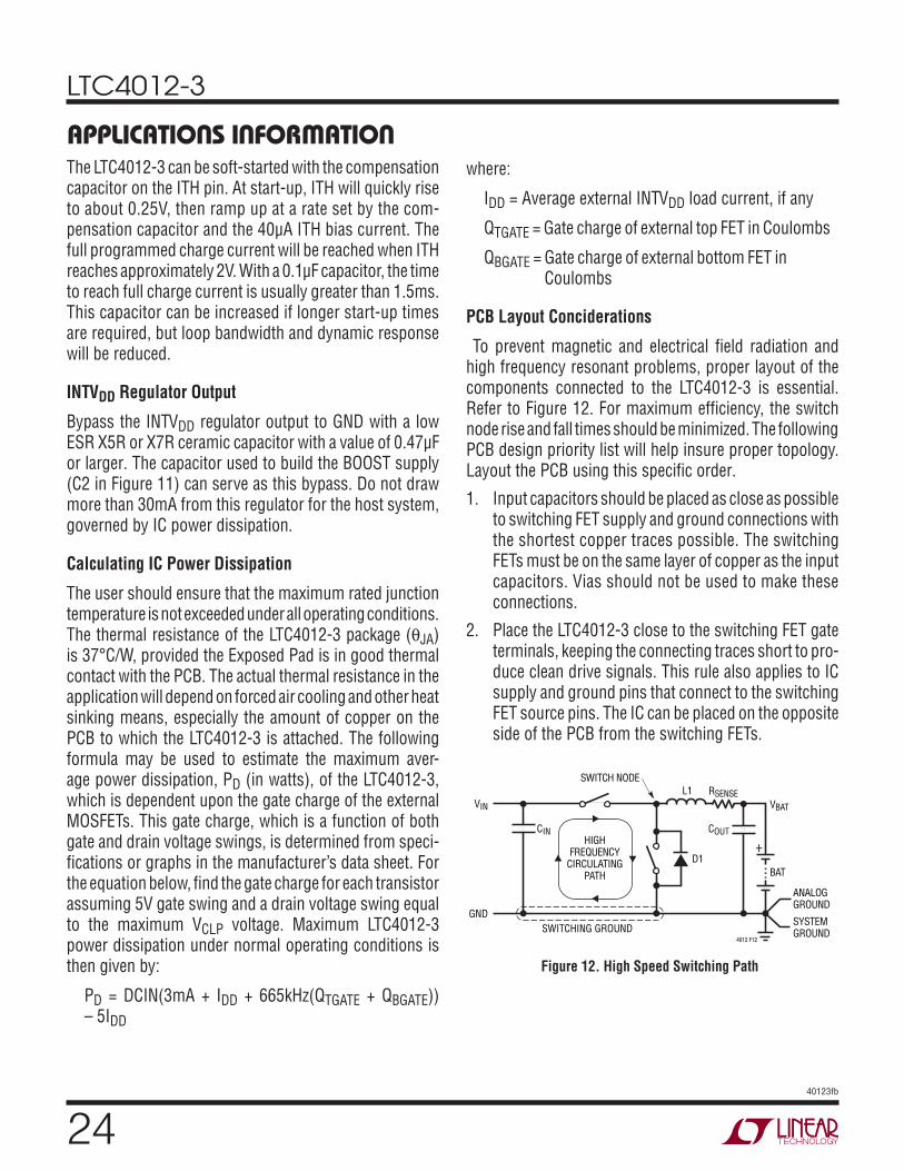
12. For best current programming accuracy, provide a Kelvin connection from RSENSE to CSP and CSN. See Figure 13 for an example.
13. It is important to minimize parasitic capacitance on the CSP and CSN pins. The traces connecting these pins to their respective resistors should be as short as possible.
applicaTions inForMaTion
Figure 13. Kelvin Sensing of Charge Current
TO CSPRIN
4012 F13
DIRECTION OF CHARGING CURRENT
RSENSE
TO CSNRIN
��40123fb
LTC4012-3
package DescripTion
4.00 ± 0.10
4.00 ± 0.10
NOTE:1. DRAWING IS PROPOSED TO BE MADE A JEDEC PACKAGE OUTLINE MO-220 VARIATION (WGGD-1)—TO BE APPROVED2. DRAWING NOT TO SCALE3. ALL DIMENSIONS ARE IN MILLIMETERS4. DIMENSIONS OF EXPOSED PAD ON BOTTOM OF PACKAGE DO NOT INCLUDE MOLD FLASH. MOLD FLASH, IF PRESENT, SHALL NOT EXCEED 0.15mm ON ANY SIDE5. EXPOSED PAD SHALL BE SOLDER PLATED6. SHADED AREA IS ONLY A REFERENCE FOR PIN 1 LOCATION ON THE TOP AND BOTTOM OF PACKAGE
PIN 1TOP MARK(NOTE 6)
0.40 ± 0.10
2019
1
2
BOTTOM VIEW—EXPOSED PAD
2.00 REF2.45 ± 0.10
0.75 ± 0.05 R = 0.115TYP
R = 0.05TYP
0.25 ± 0.05
0.50 BSC
0.200 REF
0.00 – 0.05
(UF20) QFN 01-07 REV A
RECOMMENDED SOLDER PAD PITCH AND DIMENSIONSAPPLY SOLDER MASK TO AREAS THAT ARE NOT SOLDERED
0.70 ±0.05
0.25 ±0.050.50 BSC
2.00 REF 2.45 ± 0.05
3.10 ± 0.05
4.50 ± 0.05
PACKAGE OUTLINE
PIN 1 NOTCHR = 0.20 TYPOR 0.35 45°CHAMFER
2.45 ± 0.10
2.45 ± 0.05
UF Package20-Lead Plastic QFN (4mm × 4mm)
(Reference LTC DWG # 05-08-1710 Rev A)
��40123fb
LTC4012-3
Information furnished by Linear Technology Corporation is believed to be accurate and reliable. However, no responsibility is assumed for its use. Linear Technology Corporation makes no representa-tion that the interconnection of its circuits as described herein will not infringe on existing patent rights.
revision hisToryREV DATE DESCRIPTION PAGE NUMBER
B 3/10 I-Grade Part Added. Reflected Throughout the Data Sheet 1 to 28
(Revision history begins at Rev B)

��40123fb
LTC4012-3
Linear Technology Corporation1630 McCarthy Blvd., Milpitas, CA 95035-7417 (408) 432-1900 ● FAX: (408) 434-0507 ● www.linear.com LINEAR TECHNOLOGY CORPORATION 2009
LT 0610 REV B • PRINTED IN USA
relaTeD parTsPART NUMBER DESCRIPTION COMMENTSLTC4006 Small, High Efficiency, Fixed Voltage, Lithium-Ion
Battery Chargers with TerminationComplete Charger for 3- or 4-Cell Li-Ion Batteries, AC Adapter Current Limit and Thermistor Sensor, 16-pin SSOP Package
LTC4007 High Efficiency, Programmable Voltage, Lithium-Ion Battery Charger with Termination
Complete Charger for 3- or 4-Cell Li-Ion Batteries, AC Adapter Current Limit, Thermistor Sensor and Indicator Outputs
LTC4008/LTC4008-1 High Efficiency, Programmable Voltage/Current Battery Chargers
Constant-Current/Constant-Voltage Switching Regulator, Resistor Voltage/Current Programming, Thermistor Sensor and Indicator Outputs, AC Adapter Current Limit (Omitted on 4008-1)
LTC4009/LTC4009-1 LTC4009-2
High Efficiency, Multichemistry Battery Charger Constant-Current/Constant-Voltage Switching Regulator in a 20-Lead QFN Package, AC Adapter Current Limit, Indicator Outputs
LTC4012/LTC4012-1 LTC4012-2
High Efficiency, Multi Chemistry Battery Chargers with PowerPath Control
Constant-Current/Constant-Voltage Switching Regulator in a 20-Lead QFN Package, AC Adaptor Current Limit PFET Input Ideal Diode Control, 3 Indicator Outputs
LTC4060 Standalone Linear NiMH/NiCd Fast Charger Complete NiMH/NiCd Charger in a Small 16-Pin Package, No Sense Resistor or Blocking Diode Required
LTC4411 2.6A Low Loss Idea Diode No External MOSFET, Automatic Switching Between DC sources, 140mΩ On Resistance in ThinSOTTM package
LTC4412/LTC4412HV Low Loss PowerPath Controllers Very Low Loss Replacement for Power Supply ORing Diodes Using Minimal External Complements, Operates up to 28V (36V for HV)
LTC4413 Dual 2.6A, 2.5V to 5.5V Ideal Diodes Low Loss Replacement for ORing Diodes, 100mΩ On ResistanceLTC4414 36V, Low Loss PowerPath Controller for Large PFETs Low Loss Replacement for ORing Diodes, Operates up to 36VLTC4416 Dual Low Loss PowerPath Controllers Low Loss Replacement for ORing Diodes, Operates up to 36V, Drives
Large PFETs, Programmable, Autonomous Switching
Typical applicaTion12.6V 4 Amp Charger
CLP
FROMADAPTER
15V AT 4A
BULKCHARGE
C40.1µF R8
5.1k R14100k
Q5
R150Ω*
D1 7
4
5
2
3
1
20
19
18 D3
17
16
21
15
14
11
10
Q1
9R12294k
C1010pF
8
12
13
6
R725mΩ
R9 3.01k
C50.1µF
C62µF
Q2
Q3D4
L14.7µH
R1125mΩ
12.6VLi-IonBATTERY
DCIN
CHRG
C20.1µF
R13k
R
R46.04k
R210k
R526.7k
R653.6k
LTC4012-3
ICL
SHDN
ITH
PROG
CLN
BOOSTGND
INFET
TGATE
SW
INTVDD
BGATETO/FROMMCU
GND
CSP
CSN
BATFBDIV
VFB
C810µF
POWER TO SYSTEM
TO POWER SYSTEM LOAD WHEN ADAPTER IS NOT
PRESENT, USE SCHOTTKY DIODE D5 OR
THE COMBINATION OF R14, R2D6 AND Q4
D618VZENER
C10.1µF
C34.7nF
C910µF
R10 3.01k
R1331.2k
40123 TA03
D3: CMDSH-3D4: MBR230LSFT1Q1: 2N7002Q2, Q3: Si7218DNQ4, Q5: Si7423DN L1: 1HLP-2525CZER4R7M11 *: SEE TGATE BOOST SUPPLY IN APPLICATIONS INFORMATION
+
D5
Q4
OR