ltc2209 - 16-bit, 160msps adc • • • d0 pga shdn dith mode lvds rand vcm analog input 2209 ta01...
TRANSCRIPT

LTC2209
12209fb
16-Bit, 160Msps ADC
The LTC®2209 is a 160Msps 16-bit A/D converter designed for digitizing high frequency, wide dynamic range signals with input frequencies up to 700MHz. The input range of the ADC can be optimized with the PGA front end.
The LTC2209 is perfect for demanding communications applications, with AC performance that includes 77.3dBFS Noise Floor and 100dB spurious free dynamic range (SFDR). Ultra low jitter of 70fsRMS allows undersampling of high input frequencies with excellent noise performance. Maximum DC specs include ±5.5LSB INL, ±1LSB DNL (no missing codes).
The digital output can be either differential LVDS or single-ended CMOS. There are two format options for the CMOS outputs: a single bus running at the full data rate or demultiplexed busses running at half data rate. A separate output power supply allows the CMOS output swing to range from 0.5V to 3.6V.
The ENC+ and ENC– inputs may be driven differentially or single-ended with a sine wave, PECL, LVDS, TTL or CMOS inputs. An optional clock duty cycle stabilizer al-lows high performance at full speed with a wide range of clock duty cycles.
n Telecommunicationsn Receiversn Cellular Base Stationsn Spectrum Analysisn Imaging Systemsn ATE
n Sample Rate: 160Mspsn 77.3dBFS Noise Floorn 100dB SFDRn SFDR >84dB at 250MHz (1.5VP-P Input Range)n PGA Front End (2.25VP-P or 1.5VP-P Input Range)n 700MHz Full Power Bandwidth S/Hn Optional Internal Dithern Optional Data Output Randomizern LVDS or CMOS Outputsn Single 3.3V Supplyn Power Dissipation: 1.53Wn Clock Duty Cycle Stabilizern Pin-Compatible Family: 130Msps: LTC2208 (16-Bit), LTC2208-14 (14-Bit) 105Msps: LTC2217 (16-Bit)n 64-Pin (9mm × 9mm) QFN Package
64k Point FFT, fIN = 15.1MHz, –1dBFS, PGA = 0
Features
applications
Description
typical application
L, LT, LTC and LTM are registered trademarks of Linear Technology Corporation. All other trademarks are the property of their respective owners.
–
+S/HAMP
CORRECTIONLOGIC AND
SHIFT REGISTER
OUTPUTDRIVERS
16-BITPIPELINEDADC CORE
INTERNAL ADCREFERENCEGENERATOR
1.25VCOMMON MODEBIAS VOLTAGE
CLOCK/DUTYCYCLE
CONTROL
D15•••
D0
PGA SHDN DITH MODE LVDS RAND
VCM
ANALOGINPUT
2209 TA01
CMOSORLVDS
0.5V TO 3.6V
3.3V
3.3V
SENSE
OGND
OVDD
2.2µF 1µF
1µF 1µF 1µF
VDD
GND
ADC CONTROL INPUTS
AIN+
ENC +
AIN–
ENC –
OFCLKOUT
FREQUENCY (MHz)0
AMPL
ITUD
E (d
BFS)
–100
–30–20–10
0
20 40 50
2209 TA01b
–120
–60
–80
–110
–40–50
–130
–70
–90
10 30 7060 80

LTC2209
22209fb
LEAD FREE FINISH TAPE AND REEL PART MARKING* PACKAGE DESCRIPTION TEMPERATURE RANGE
LTC2209CUP#PBF LTC2209CUP#TRPBF LTC2209UP 64-Lead (9mm × 9mm) Plastic QFN 0°C to 70°C
LTC2209IUP#PBF LTC2209IUP#TRPBF LTC2209UP 64-Lead (9mm × 9mm) Plastic QFN –40°C to 85°C
LEAD BASED FINISH TAPE AND REEL PART MARKING* PACKAGE DESCRIPTION TEMPERATURE RANGE
LTC2209CUP LTC2209CUP#TR LTC2209UP 64-Lead (9mm × 9mm) Plastic QFN 0°C to 70°C
LTC2209IUP LTC2209IUP#TR LTC2209UP 64-Lead (9mm × 9mm) Plastic QFN –40°C to 85°C
Consult LTC Marketing for parts specified with wider operating temperature ranges. *The temperature grade is identified by a label on the shipping container.For more information on lead free part marking, go to: http://www.linear.com/leadfree/ For more information on tape and reel specifications, go to: http://www.linear.com/tapeandreel/
pin conFigurationabsolute MaxiMuM ratingsOVDD = VDD (Notes 1 and 2)
The l denotes the specifications which apply over the full operating temperature range, otherwise specifications are at TA = 25°C. (Note 4)
Supply Voltage (VDD) ................................... –0.3V to 4VDigital Output Ground Voltage (OGND) ........ –0.3V to 1VAnalog Input Voltage (Note 3) ...... –0.3V to (VDD + 0.3V)Digital Input Voltage..................... –0.3V to (VDD + 0.3V)Digital Output Voltage ................ –0.3V to (OVDD + 0.3V)Power Dissipation ............................................ 2500mWOperating Temperature Range LTC2209C ................................................ 0°C to 70°C LTC2209I .............................................–40°C to 85°CStorage Temperature Range ..................–65°C to 150°CDigital Output Supply Voltage (OVDD) .......... –0.3V to 4V
orDer inForMation
converter characteristics
PARAMETER CONDITIONS MIN TYP MAX UNITS
Integral Linearity Error Differential Analog Input (Note 5) l ±1.5 ±5.5 LSB
Differential Linearity Error Differential Analog Input l ±0.3 ±1 LSB
Offset Error (Note 6) l ±2 ±10 mV
Offset Drift ±10 µV/°C
Gain Error External Reference l ±0.2 ±2 %FS
Full-Scale Drift Internal Reference External Reference
±30 ±15
ppm/°C ppm/°C
Transition Noise External Reference 3 LSBRMS
TOP VIEW
65GND
SENSE 1GND 2VCM 3GND 4VDD 5VDD 6GND 7AIN
+ 8AIN
– 9GND 10GND 11
ENC+ 12ENC– 13GND 14VDD 15VDD 16
48 D11+/DA6 47 D11–/DA5 46 D10+/DA4 45 D10–/DA344 D9+/DA2 43 D9–/DA142 D8+/DA041 D8–/CLKOUTA40 CLKOUT+/CLKOUTB 39 CLKOUT–/OFB38 D7+/DB1537 D7–/DB1436 D6+/DB1335 D6–/DB1234 D5+/DB1133 D5–/DB10
64 P
GA63
RAN
D62
MOD
E61
LVD
S60
OF+ /O
FA59
OF– /D
A15
58 D
15+ /D
A14
57 D
15/D
A13
56 D
14+ /D
A12
55 D
14–– /D
A11
54 D
13+ /D
A10
53 D
13– –/D
A952
D12
+ /DA8
51 D
12/D
A750
OGN
D49
OV D
D
V DD
17GN
D 18
SHDN
19
DITH
20
D0– /D
B0 2
1DO
+ /DB1
22
D1– /D
B2 2
3D1
+ /DB3
24
D2– /D
B4 2
5D2
+ /DB5
26
D3– /D
B6 2
7D3
+ /DB7
28
D4– /D
B8 2
9 D
4+ /DB9
30
OGN
D 31
OV D
D 32
TJMAX = 150°C, θJA = 20°C/W
EXPOSED PAD (PIN 65) IS GND, MUST BE SOLDERED TO PCB

LTC2209
32209fb
The l denotes the specifications which apply over the full operating temperature range, otherwise specifications are at TA = 25°C. (Note 4)
The l denotes the specifications which apply over the full operating temperature range, otherwise specifications are at TA = 25°C. AIN = –1dBFS. (Note 4)
analog input
DynaMic accuracy
SYMBOL PARAMETER CONDITIONS MIN TYP MAX UNITS
VIN Analog Input Range (AIN+ – AIN
–) 3.135V ≤ VDD ≤ 3.465V 1.5 or 2.25 VP-P
VIN, CM Analog Input Common Mode Differential Input (Note 7) l 1 1.25 1.5 V
IIN Analog Input Leakage Current 0V ≤ AIN+, AIN
– ≤ VDD l –1 1 µA
ISENSE SENSE Input Leakage Current 0V ≤ SENSE ≤ VDD l –3 3 µA
IMODE MODE Pin Pull-Down Current to GND 10 µA
ILVDS LVDS Pin Pull-Down Current to GND 10 µA
CIN Analog Input Capacitance Sample Mode ENC+ < ENC–
Hold Mode ENC+ > ENC–6.6 1.8
pF pF
tAP Sample-and-Hold Aperture Delay Time
1.0 ns
tJITTER Sample-and-Hold Acquisition Delay Time Jitter
70 fs RMS
CMRR Analog Input Common Mode Rejection Ratio
1V < (AIN+ = AIN
–) <1.5V 80 dB
BW-3dB Full Power Bandwidth RS < 25Ω 700 MHz
SYMBOL PARAMETER CONDITIONS MIN TYP MAX UNITS
SNR Signal-to-Noise Ratio 5MHz Input (2.25V Range, PGA = 0) 5MHz Input (1.5V Range, PGA = 1)
77.1 75
dBFS dBFS
30MHz Input (2.25V Range, PGA = 0) 30MHz Input (1.5V Range, PGA = 1)
l 75.5 76.8 74.9
dBFS dBFS
70MHz Input (2.25V Range, PGA = 0) 70MHz Input (1.5V Range, PGA = 1)
76.9 74.7
dBFS dBFS
140MHz Input (2.25V Range, PGA = 0) 140MHz Input (1.5V Range, PGA = 1)
l
71.9
76.6 73.9
dBFS dBFS
250MHz Input (2.25V Range, PGA = 0) 250MHz Input (1.5V Range, PGA =1 )
75 73.5
dBFS dBFS
SFDR Spurious Free Dynamic Range 2nd or 3rd Harmonic
5MHz Input (2.25V Range, PGA = 0) 5MHz Input (1.5V Range, PGA = 1)
100 100
dBc dBc
30MHz Input (2.25V Range, PGA = 0) 30MHz Input (1.5V Range, PGA = 1)
l 84 94 100
dBc dBc
70MHz Input (2.25V Range, PGA = 0) 70MHz Input (1.5V Range, PGA = 1)
88 88
dBc dBc
140MHz Input (2.25V Range, PGA = 0) 140MHz Input (1.5V Range, PGA = 1)
l
81
84 88
dBc dBc
250MHz Input (2.25V Range, PGA = 0) 250MHz Input (1.5V Range, PGA = 1)
75 84
dBc dBc

LTC2209
42209fb
The l denotes the specifications which apply over the full operating temperature range, otherwise specifications are at TA = 25°C. AIN = –1dBFS unless otherwise noted. (Note 4)DynaMic accuracy
SYMBOL PARAMETER CONDITIONS MIN TYP MAX UNITS
SFDR Spurious Free Dynamic Range 4th Harmonic or Higher
5MHz Input (2.25V Range, PGA = 0) 5MHz Input (1.5V Range, PGA = 1)
100 100
dBc dBc
30MHz Input (2.25V Range, PGA = 0) 30MHz Input (1.5V Range, PGA = 1)
l 88 100 100
dBc dBc
70MHz Input (2.25V Range, PGA = 0) 70MHz Input (1.5V Range, PGA = 1)
100 100
dBc dBc
140MHz Input (2.25V Range, PGA = 0) 140MHz Input (1.5V Range, PGA = 1)
l
84
95 95
dBc dBc
250MHz Input (2.25V Range, PGA = 0) 250MHz Input (1.5V Range, PGA = 1)
90 90
dBc dBc
S/(N+D) Signal-to-Noise Plus Distortion Ratio
5MHz Input (2.25V Range, PGA = 0) 5MHz Input (1.5V Range, PGA = 1)
77.1 75
dBFS dBFS
30MHz Input (2.25V Range, PGA = 0) 30MHz Input (1.5V Range, PGA = 1)
l 75.3 76.7 74.9
dBFS dBFS
70MHz Input (2.25V Range, PGA = 0) 70MHz Input (1.5V Range, PGA = 1)
76.8 74.7
dBFS dBFS
140MHz Input (2.25V Range, PGA = 0) 140MHz Input (1.5V Range, PGA = 1)
l
71.7
75.7 74.2
dBFS dBFS
250MHz Input (2.25V Range, PGA = 0) 250MHz Input (1.5V Range, PGA = 1)
73.3 72.6
dBFS dBFS
SFDR Spurious Free Dynamic Range at –25dBFS Dither “OFF”
5MHz Input (2.25V Range, PGA = 0) 5MHz Input (1.5V Range, PGA = 1)
105 105
dBFS dBFS
30MHz Input (2.25V Range, PGA = 0) 30MHz Input (1.5V Range, PGA = 1)
105 105
dBFS dBFS
70MHz Input (2.25V Range, PGA = 0) 70MHz Input (1.5V Range, PGA = 1)
105 105
dBFS dBFS
14 0MHz Input (2.25V Range, PGA = 0) 140MHz Input (1.5V Range, PGA = 1)
100 100
dBFS dBFS
250MHz Input (2.25V Range, PGA = 0) 250MHz Input (1.5V Range, PGA = 1)
100 100
dBFS dBFS
SFDR Spurious Free Dynamic Range at –25dBFS Dither “ON”
5MHz Input (2.25V Range, PGA = 0) 5MHz Input (1.5V Range, PGA = 1)
115 115
dBFS dBFS
30MHz Input (2.25V Range, PGA = 0) 30MHz Input (1.5V Range, PGA = 1)
l 100 115 115
dBFS dBFS
70MHz Input (2.25V Range, PGA = 0) 70MHz Input (1.5V Range, PGA = 1)
115 115
dBFS dBFS
140MHz Input (2.25V Range, PGA = 0) 140MHz Input (1.5V Range, PGA = 1)
110 110
dBFS dBFS
250MHz Input (2.25V Range, PGA = 0) 250MHz Input (1.5V Range, PGA = 1)
105 105
dBFS dBFS

LTC2209
52209fb
The l denotes the specifications which apply over the full operating temperature range, otherwise specifications are at TA = 25°C. (Note 4)
The l denotes the specifications which apply over the full operating temperature range, otherwise specifications are at TA = 25°C. (Note 4)
coMMon MoDe bias characteristics
Digital inputs anD Digital outputs
PARAMETER CONDITIONS MIN TYP MAX UNITS
VCM Output Voltage IOUT = 0 1.15 1.25 1.35 V
VCM Output Tempco IOUT = 0 +40 ppm/°C
VCM Line Regulation 3.135V ≤ VDD ≤ 3.465V 1 mV/ V
VCM Output Resistance 1mA ≤ | IOUT | ≤ 1mA 2 Ω
SYMBOL PARAMETER CONDITIONS MIN TYP MAX UNITS
ENCODE INPUTS (ENC+, ENC–)
VID Differential Input Voltage (Note 7) l 0.2 V
VICM Common Mode Input Voltage Internally Set Externally Set (Note 7)
1.2
1.6 3.0
V V
RIN Input Resistance (See Figure 2) 6 kΩCIN Input Capacitance (Note 7) 3 pF
LOGIC INPUTS (DITH, PGA, SHDN, RAND)
VIH High Level Input Voltage VDD = 3.3V l 2 V
VIL Low Level Input Voltage VDD = 3.3V l 0.8 V
IIN Digital Input Current VIN = 0V to VDD l ±10 µA
CIN Digital Input Capacitance (Note 7) 1.5 pF
LOGIC OUTPUTS (CMOS MODE)
OVDD = 3.3V
VOH High Level Output Voltage VDD = 3.3V IO = –10µA IO = –200µA
l
3.1
3.299 3.29
V V
VOL Low Level Output Voltage VDD = 3.3V IO = 160µA IO = 1.6mA
l
0.01 0.10
0.4
V V
ISOURCE Output Source Current VOUT = 0V –50 mA
ISINK Output Sink Current VOUT = 3.3V 50 mA
OVDD = 2.5V
VOH High Level Output Voltage VDD = 3.3V, IO = –200µA 2.49 V
VOL Low Level Output Voltage VDD = 3.3V, IO = 1.60mA 0.1 V
OVDD = 1.8V
VOH High Level Output Voltage VDD = 3.3V, IO = –200µA 1.79 V
VOL Low Level Output Voltage VDD = 3.3V, IO = 1.60mA 0.1 V
LOGIC OUTPUTS (LVDS MODE)
STANDARD LVDS
VOD Differential Output Voltage 100Ω Differential Load l 247 350 454 mV
VOS Output Common Mode Voltage 100Ω Differential Load l 1.125 1.2 1.375 V
LOW POWER LVDS
VOD Differential Output Voltage 100Ω Differential Load l 125 175 250 mV
VOS Output Common Mode Voltage 100Ω Differential Load l 1.125 1.2 1.375 V
LTC2209
62209fb
The l denotes the specifications which apply over the full operating temperature range, otherwise specifications are at TA = 25°C. AIN = –1dBFS. (Note 4)
The l denotes the specifications which apply over the full operating temperature range, otherwise specifications are at TA = 25°C. (Note 4)
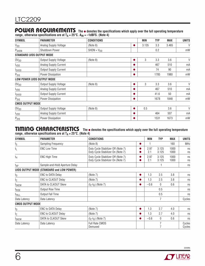
power requireMents
tiMing characteristics
SYMBOL PARAMETER CONDITIONS MIN TYP MAX UNITS
VDD Analog Supply Voltage (Note 8) l 3.135 3.3 3.465 V
PSHDN Shutdown Power SHDN = VDD 0.2 mW
STANDARD LVDS OUTPUT MODE
OVDD Output Supply Voltage (Note 8) l 3 3.3 3.6 V
IVDD Analog Supply Current l 467 510 mA
IOVDD Output Supply Current l 74 90 mA
PDIS Power Dissipation l 1785 1980 mW
LOW POWER LVDS OUTPUT MODE
OVDD Output Supply Voltage (Note 8) l 3 3.3 3.6 V
IVDD Analog Supply Current l 467 510 mA
IOVDD Output Supply Current l 41.6 50 mA
PDIS Power Dissipation l 1678 1848 mW
CMOS OUTPUT MODE
OVDD Output Supply Voltage (Note 8) l 0.5 3.6 V
IVDD Analog Supply Current l 464 507 mA
PDIS Power Dissipation l 1531 1673 mW
SYMBOL PARAMETER CONDITIONS MIN TYP MAX UNITS
fS Sampling Frequency (Note 8) l 1 160 MHz
tL ENC Low Time Duty Cycle Stabilizer Off (Note 7) Duty Cycle Stabilizer On (Note 7)
l
l
2.97 2.1
3.125 3.125
1000 1000
ns ns
tH ENC High Time Duty Cycle Stabilizer Off (Note 7) Duty Cycle Stabilizer On (Note 7)
l
l
2.97 2.1
3.125 3.125
1000 1000
ns ns
tAP Sample-and-Hold Aperture Delay 1 ns
LVDS OUTPUT MODE (STANDARD and LOW POWER)
tD ENC to DATA Delay (Note 7) l 1.3 2.5 3.8 ns
tC ENC to CLKOUT Delay (Note 7) l 1.3 2.5 3.8 ns
tSKEW DATA to CLKOUT Skew (tC-tD) (Note 7) l –0.6 0 0.6 ns
tRISE Output Rise Time 0.5 ns
tFALL Output Fall Time 0.5 ns
Data Latency Data Latency 7 Cycles
CMOS OUTPUT MODE
tD ENC to DATA Delay (Note 7) l 1.3 2.7 4.0 ns
tC ENC to CLKOUT Delay (Note 7) l 1.3 2.7 4.0 ns
tSKEW DATA to CLKOUT Skew (tC-tD) (Note 7) l –0.6 0 0.6 ns
Data Latency Data Latency Full Rate CMOS Demuxed
7 7
Cycles Cycles
LTC2209
72209fb
Note 1: Stresses beyond those listed under Absolute Maximum Ratings may cause permanent damage to the device. Exposure to any Absolute Maximum Rating condition for extended periods may affect device reliability and lifetime.Note 2: All voltage values are with respect to GND, with GND and OGND shorted (unless otherwise noted).Note 3: When these pin voltages are taken below GND or above VDD, they will be clamped by internal diodes. This product can handle input currents of greater than 100mA below GND or above VDD without latchup.Note 4: VDD = 3.3V, fSAMPLE = 160MHz, LVDS outputs, differential ENC+/ENC– = 2VP-P sine wave with 1.6V common mode, input range = 2.25VP-P with differential drive (PGA = 0), unless otherwise specified.
Note 5: Integral nonlinearity is defined as the deviation of a code from a “best fit straight line” to the transfer curve. The deviation is measured from the center of the quantization band.Note 6: Offset error is the offset voltage measured from –1/2LSB when the output code flickers between 0000 0000 0000 0000 and 1111 1111 1111 1111 in 2’s complement output mode.Note 7: Guaranteed by design, not subject to test.Note 8: Recommended operating conditions.
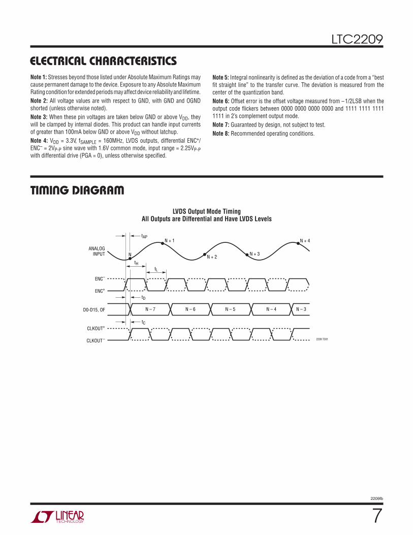
LVDS Output Mode Timing All Outputs are Differential and Have LVDS Levels
electrical characteristics
tiMing DiagraM
tH
tD
tC
tL
N – 7 N – 6 N – 5 N – 4 N – 3
ANALOGINPUT
ENC–
ENC+
CLKOUT–
CLKOUT+
D0-D15, OF
2209 TD01
tAPN + 1
N + 2
N + 4
N + 3N
LTC2209
82209fb
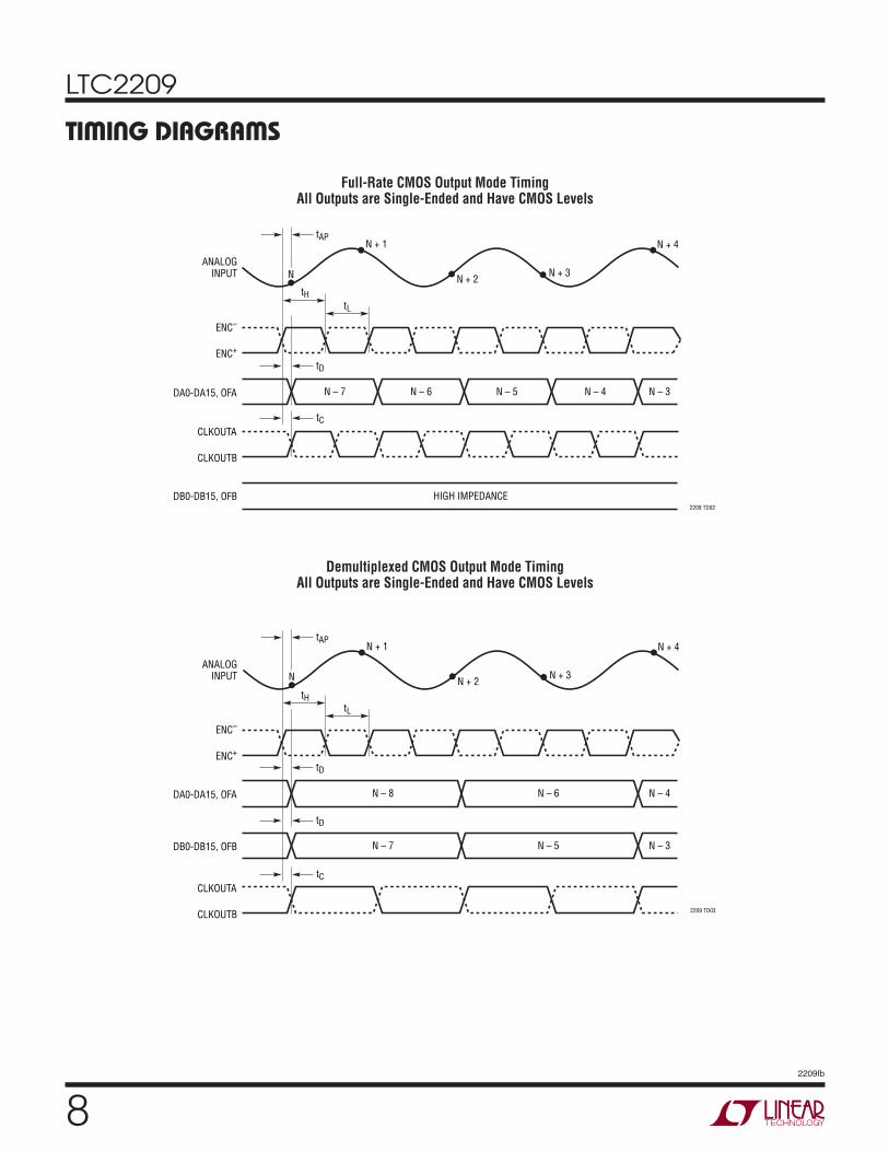
Demultiplexed CMOS Output Mode TimingAll Outputs are Single-Ended and Have CMOS Levels
Full-Rate CMOS Output Mode TimingAll Outputs are Single-Ended and Have CMOS Levels
tiMing DiagraMs
tAP
ANALOGINPUT
tH
tD
tC
tL
N – 7 N – 6 N – 5 N – 4 N – 3
ENC–
ENC+
CLKOUTA
CLKOUTB
DA0-DA15, OFA
DB0-DB15, OFB2209 TD02
HIGH IMPEDANCE
N + 1
N + 2
N + 4
N + 3N
tH
tD
tD
tC
tL
N – 8 N – 6 N – 4
N – 7 N – 5 N – 3
ENC–
ENC+
CLKOUTA
CLKOUTB
DA0-DA15, OFA
DB0-DB15, OFB
2209 TD03
tAP
ANALOGINPUT
N + 1
N + 2
N + 4
N + 3N

LTC2209
92209fb
Integral Nonlinearity (INL) vs Output Code
Differential Nonlinearity (DNL) vs Output Code AC Grounded Input Histogram
64k Point 2-Tone FFT, fIN = 21.14MHz and 14.25MHz, –7dBFS, PGA = 0
64k Point FFT, fIN = 15.1MHz, –20dBFS, PGA = 0, Dither “Off”
64k Point FFT, fIN = 15.1MHz, –20dBFS, PGA = 0, Dither “On”
64k Point FFT, fIN = 15.1MHz, –1dBFS, PGA = 0
128k Point FFT, fIN = 4.9MHz, –1dBFS, PGA = 0
typical perForMance characteristics
64k Point 2-Tone FFT, fIN = 20.2MHz and 25.3MHz, –25dBFS, PGA = 0
OUTPUT CODE0
INL
ERRO
R (L
SB)
0
1.0
–1.0
65536
2209 G01
–2.016384 32768 49152
2.0
1.5
–1.5
0.5
–0.5
OUTPUT CODE0
–1.0
DNL
ERRO
R (L
SB)
–0.8
–0.4
–0.2
0
1.0
0.4
16384 32768
2209 G02
–0.6
0.6
0.8
0.2
49152 65536OUTPUT CODE
32797 32807 32817 32827
COUN
T 21000
7000
14000
28000
35000
2209 G03
0
FREQUENCY (MHz)
–130
AMPL
ITUD
E (d
BFS)
–100–110–120
–80–90
–30–40–50–60–70
0–10–20
2209 G04
0 20 40 5010 30 7060 80FREQUENCY (MHz)
0
AMPL
ITUD
E (d
BFS)
–100
–30–20–10
0
20 40 50
2209 G05
–120
–60
–80
–110
–40–50
–130
–70
–90
10 30 7060 80FREQUENCY (MHz)
–130
AMPL
ITUD
E (d
BFS)
–100–110–120
–80–90
–30–40–50–60–70
0–10–20
2209 G06
0 20 40 5010 30 7060 80
FREQUENCY (MHz)
–130
AMPL
ITUD
E (d
BFS)
–100–110–120
–80–90
–30–40–50–60–70
0–10–20
2209 G07
0 20 40 5010 30 7060 80FREQUENCY (MHz)
–130
AMPL
ITUD
E (d
BFS)
–100–110–120
–80–90
–30–40–50–60–70
0–10–20
2209 G08
0 20 40 5010 30 7060 80FREQUENCY (MHz)
AMPL
ITUD
E (d
BFS)
2209 G09
–130
–100–110–120
–80–90
–30–40–50–60–70
0–10–20
0 20 40 5010 30 7060 80

LTC2209
102209fb
SFDR vs Input Level, fIN = 15MHz, PGA = 0, Dither “On”
64k Point FFT, fIN = 30.1MHz, –1dBFS, PGA = 0
128k Point FFT, fIN = 30.1MHz, –25dBFS, PGA = 0, Dither “On”
64k Point FFT, fIN = 70.1MHz, –1dBFS, PGA = 0
64k Point FFT, fIN = 70.1MHz, –20dBFS, PGA = 0
128k Point FFT, fIN = 70.1MHz, –25dBFS, PGA = 0, Dither “On”
SFDR vs Input Level, fIN = 15MHz, PGA = 0, Dither “Off”
64k Point FFT, fIN = 70.1MHz, –10dBFS, PGA = 0
typical perForMance characteristics
SFDR vs Input Level, fIN = 70.2MHz, PGA = 0, Dither “Off”
INPUT LEVEL (dBFS)–80
0
SFDR
(dB
c AN
D dB
FS)
20
40
60
130
110
90
70
50
30
10
100
–70 –50 –40 0
120
80
–60 –30 –20 –10
2209 G10 INPUT LEVEL (dBFS)–80
SFDR
(dB
c AN
D dB
FS)
–70 –50 –40 0–60 –30 –20 –10
2209 G11
0
20
40
60
130
110
90
70
50
30
10
100
120
80
–130
–100–110–120
–80–90
–30–40–50–60–70
–10–20
0 20 40 5010 30 7060 80FREQUENCY (MHz)
AMPL
ITUD
E (d
BFS)
2209 G12
0
FREQUENCY (MHz)
AMPL
ITUD
E (d
BFS)
–100
–30–20–10
0
2209 G13
–120
–60
–80
–110
–40–50
–130
–70
–90
0 20 40 5010 30 7060 80 0 20 40 5010 30 7060 80FREQUENCY (MHz)
AMPL
ITUD
E (d
BFS)
–100
–30–20–10
0
2209 G14
–120
–60
–80
–110
–40–50
–130
–70
–90
FREQUENCY (MHz)
AMPL
ITUD
E (d
BFS)
–100
–30–20–10
0
2209 G15
–120
–60
–80
–110
–40–50
–130
–70
–90
0 20 40 5010 30 7060 80
FREQUENCY (MHz)
AMPL
ITUD
E (d
BFS)
–100
–30–20–10
0
2209 G16
–120
–60
–80
–110
–40–50
–130
–70
–90
0 20 40 5010 30 7060 80FREQUENCY (MHz)
AMPL
ITUD
E (d
BFS)
–100
–30–20–10
0
2209 G17
–120
–60
–80
–110
–40–50
–130
–70
–90
0 20 40 5010 30 7060 80INPUT LEVEL (dBFS)
–80
SFDR
(dBc
AND
dBF
S)
–60 –40 –30
2209 G18
–70 –50 –20 –10 00
20
40
60
130
110
90
70
50
30
10
100
120
80

LTC2209
112209fb
64k Point 2-Tone FFT, fIN = 70.25MHz and 74.3MHz, –15dBFS, PGA = 0
64k Point 2-Tone FFT, fIN = 70.25MHz and 74.3MHz, –25dBFS, PGA = 0
64k Point FFT, fIN = 140.2 MHz, –1dBFS, PGA = 1
SFDR vs Input Level, fIN = 70.2MHz, PGA = 0, Dither “On”
64k Point 2-Tone FFT, fIN = 70.25MHz and 74.3MHz, –7dBFS, PGA = 0
SFDR vs Input Level, fIN = 140.2MHz, PGA = 1, Dither “On”
64k Point FFT, fIN = 250.1MHz, –1dBFS, PGA = 1
typical perForMance characteristics
SFDR vs Input Level, fIN = 140.2MHz, PGA = 1, Dither “Off”
64k Point FFT, fIN = 170.1MHz, –1dBFS, PGA = 1
INPUT LEVEL (dBFS)–80
SFDR
(dBc
AND
dBF
S)
–60 –40 –30
2209 G19
–70 –50 –20 –10 00
20
40
60
130
110
90
70
50
30
10
100
120
80
FREQUENCY (MHz)
AMPL
ITUD
E (d
BFS)
–100
–30–20–10
0
2209 G20
–120
–60
–80
–110
–40–50
–130
–70
–90
0 20 40 5010 30 7060 80FREQUENCY (MHz)
AMPL
ITUD
E (d
BFS)
–100
–30–20–10
0
2209 G21
–120
–60
–80
–110
–40–50
–130
–70
–90
0 20 40 5010 30 7060 80
FREQUENCY (MHz)
AMPL
ITUD
E (d
BFS)
–100
–30–20–10
0
2209 G22
–120
–60
–80
–110
–40–50
–130
–70
–90
0 20 40 5010 30 7060 80FREQUENCY (MHz)
AMPL
ITUD
E (d
BFS)
–100
–30–20–10
0
2209 G23
–120
–60
–80
–110
–40–50
–130
–70
–90
0 20 40 5010 30 7060 80INPUT LEVEL (dBFS)
–80
SFDR
(dBc
AND
dBF
S)
–60 –40 –30
2209 G24
–70 –50 –20 –10 00
20
40
60
130
110
90
70
50
30
10
100
120
80
INPUT LEVEL (dBFS)–80
SFDR
(dBc
AND
dBF
S)
–60 –40 –30
2209 G25
–70 –50 –20 –10 00
20
40
60
130
110
90
70
50
30
10
100
120
80
FREQUENCY (MHz)
AMPL
ITUD
E (d
BFS)
–100
–30–20–10
0
2209 G26
–120
–60
–80
–110
–40–50
–130
–70
–90
0 20 40 5010 30 7060 80FREQUENCY (MHz)
AMPL
ITUD
E (d
BFS)
–100
–30–20–10
0
2209 G27
–120
–60
–80
–110
–40–50
–130
–70
–90
0 20 40 5010 30 7060 80

LTC2209
122209fb
SNR vs Input Frequency
SNR and SFDR vs Sample Rate, fIN = 5.1MHz
SNR and SFDR vs Supply Voltage (VDD), fIN = 5.1MHz
64k Point FFT, fIN = 250.1MHz, –10dBFS, PGA = 1, Dither “On”
64k Point FFT, fIN = 250.1MHz, –20dBFS, PGA = 1
64k Point FFT, fIN = 380MHz, –10dBFS, PGA = 1
SFDR (HD2 and HD3) vs Input Frequency
64k Point FFT, fIN = 380MHz, –1dBFS, PGA = 1
IVDD vs Sample Rate, 5MHz Sine, –1dBFS
typical perForMance characteristics
FREQUENCY (MHz)
AMPL
ITUD
E (d
BFS)
–100
–30–20–10
0
2209 G28
–120
–60
–80
–110
–40–50
–130
–70
–90
0 20 40 5010 30 7060 80FREQUENCY (MHz)
AMPL
ITUD
E (d
BFS)
–100
–30–20–10
0
2209 G29
–120
–60
–80
–110
–40–50
–130
–70
–90
0 20 40 5010 30 7060 80FREQUENCY (MHz)
AMPL
ITUD
E (d
BFS)
–100
–30–20–10
0
2209 G30
–120
–60
–80
–110
–40–50
–130
–70
–90
0 20 40 5010 30 7060 80
FREQUENCY (MHz)
AMPL
ITUD
E (d
BFS)
–100
–30–20–10
0
2209 G31
–120
–60
–80
–110
–40–50
–130
–70
–90
0 20 40 5010 30 7060 80
INPUT FREQUENCY (MHz)0
SFDR
(dBc
)
80
85
90
300 500
2209 G32
75
70
65100 200 400
95
100
105
PGA = 1
PGA = 0
INPUT FREQUENCY (MHz)0
SNR
(dBF
S)
73
74
75
300 500
2209 G33
72
71
70100 200 400
76
77
78
PGA = 1
PGA = 0
SAMPLE RATE (Msps)0
SNR
AND
SFDR
(dBF
S)
90
100
200
2209 G34
80
7040 16012080
115
110
85
95
75
105
SFDR
SNR
LIMIT
SUPPLY VOLTAGE (V)2.8
SNR
AND
SFDR
(dBF
S)
90
100
2209 G35
80
703.2 3.63.0 3.4
110
85
95
75
105LOWER LIMIT
UPPER LIMIT
SNR
SFDR
SAMPLE RATE (Msps)0
350
I VDD
(mA)
450
400
375
475
425
500
50 100 200150
2209 G36
VDD = 3.47V
VDD = 3.13V
VDD = 3.3V

LTC2209
132209fb
SNR and SFDR vs Duty CycleInput Offset Voltage vs Temperature, 5 Units
Full-Scale Settling After Wake-Up from Shutdown or Starting Encode Clock
typical perForMance characteristics
Normalized Full Scale vs Temperature, Internal Reference, 5 Units
Mid-Scale Settling After Wake-Up from Shutdown or Starting Encode Clock
SFDR vs Analog Input Common Mode Voltage, 5MHz and 70MHz, –1dBFS, PGA = 0
DUTY CYCLE (%)30
SFDR
AND
SNR
(dBF
S)
90
70
2209 G37
70
10
30
50
40 50 60
110
SNR DCS OFFSNR DCS ONSFDR DCS OFFSFDR DCS ON
TEMPERATURE (°C)–40
0.995
NORM
ALIZ
ED F
ULL
SCAL
E
0.996
0.997
0.998
0.999
1.000
1.004
1.003
1.002
1.001
1.005
–20 0 20 40
2209 G38
60 80TEMPERATURE (°C)
OFFS
ET V
OLTA
GE (m
V)
–3
–4
–5
–1
2
1
0
–2
5
4
3
2209 G39
–40 –20 0 20 40 60 80
ANALOG INPUT COMMON MODE VOLTAGE (V)0.50
60
SFDR
(dBc
)
70
80
90
0.75 1.00 1.25 1.50
2209 G40
1.75
100
110
65
75
85
95
105
2.00
70MHz
5MHz
TIME AFTER WAKE-UP OR CLOCK START (µs)0
FULL
-SCA
LE E
RROR
(%)
0
0.4
500
2209 G41
–1.0250
1.0
0.8
0.2
0.6
–0.4
–0.8
–0.2
–0.6
TIME FROM WAKE-UP OR CLOCK START (µs)0
FULL
-SCA
LE E
RROR
(%)
0
2
1000
2209 G42
–5500
5
4
1
3
–2
–4
–1
–3

LTC2209
142209fb
For CMOS Mode. Full Rate or Demultiplexed
SENSE (Pin 1): Reference Mode Select and External Reference Input. Tie SENSE to VDD to select the internal 2.5V bandgap reference. An external reference of 2.5V or 1.25V may be used; both reference values will set a full scale ADC range of 2.25V (PGA = 0).
GND (Pins 2, 4, 7, 10, 11, 14, 18): ADC Power Ground.
VCM (Pin 3): 1.25V Output. Optimum voltage for input common mode. Must be bypassed to ground with a mini-mum of 2.2µF. Ceramic chip capacitors are recommended.
VDD (Pins 5, 6, 15, 16, 17): 3.3V Analog Supply Pin. Bypass to GND with 1µF ceramic chip capacitors.
AIN+ (Pin 8): Positive Differential Analog Input.
AIN– (Pin 9): Negative Differential Analog Input.
ENC+ (Pin 12): Positive Differential Encode Input. The sampled analog input is held on the rising edge of ENC+. Internally biased to 1.6V through a 6.2kΩ resistor. Output data can be latched on the rising edge of ENC+.
ENC– (Pin 13): Negative Differential Encode Input. The sampled analog input is held on the falling edge of ENC–. Internally biased to 1.6V through a 6.2kΩ resistor. By-pass to ground with a 0.1µF capacitor for a single-ended Encode signal.
SHDN (Pin 19): Power Shutdown Pin. SHDN = low results in normal operation. SHDN = high results in powered down analog circuitry and the digital outputs are placed in a high impedance state.
DITH (Pin 20): Internal Dither Enable Pin. DITH = low disables internal dither. DITH = high enables internal dither. Refer to Internal Dither section of this data sheet for details on dither operation.
DB0-DB15 (Pins 21-30 and 33-38): Digital Outputs, B Bus. DB15 is the MSB. Active in demultiplexed mode. The B bus is in high impedance state in full rate CMOS.
OGND (Pins 31 and 50): Output Driver Ground.
OVDD (Pins 32 and 49): Positive Supply for the Output Drivers. Bypass to ground with 1µF capacitor.
OFB (Pin 39): Over/Under Flow Digital Output for the B Bus. OFB is high when an over or under flow has occurred on the B bus. At high impedance state in full rate CMOS mode.
CLKOUTB (Pin 40): Data Valid Output. CLKOUTB will toggle at the sample rate in full rate CMOS mode or at 1/2 the sample rate in demultiplexed mode. Latch the data on the falling edge of CLKOUTB.
CLKOUTA (Pin 41): Inverted Data Valid Output. CLKOUTA will toggle at the sample rate in full rate CMOS mode or at 1/2 the sample rate in demultiplexed mode. Latch the data on the rising edge of CLKOUTA.
DA0-DA15 (Pins 42-48 and 51-59): Digital Outputs, A Bus. DA15 is the MSB. Output bus for full rate CMOS mode and demultiplexed mode.
OFA (Pin 60): Over/Under Flow Digital Output for the A Bus. OFA is high when an over or under flow has occurred on the A bus.
LVDS (Pin 61): Data Output Mode Select Pin. Connecting LVDS to 0V selects full rate CMOS mode. Connecting LVDS to 1/3VDD selects demultiplexed CMOS mode. Connecting LVDS to 2/3VDD selects Low Power LVDS mode. Connect-ing LVDS to VDD selects Standard LVDS mode.
MODE (Pin 62): Output Format and Clock Duty Cycle Stabilizer Selection Pin. Connecting MODE to 0V selects offset binary output format and disables the clock duty cycle stabilizer. Connecting MODE to 1/3VDD selects offset binary output format and enables the clock duty cycle sta-bilizer. Connecting MODE to 2/3VDD selects 2’s complement output format and enables the clock duty cycle stabilizer. Connecting MODE to VDD selects 2’s complement output format and disables the clock duty cycle stabilizer.
RAND (Pin 63): Digital Output Randomization Selection Pin. RAND low results in normal operation. RAND high selects D1-D15 to be EXCLUSIVE-ORed with D0 (the LSB). The output can be decoded by again applying an XOR operation between the LSB and all other bits. This mode of operation reduces the effects of digital output interference.
PGA (Pin 64): Programmable Gain Amplifier Control Pin. Low selects a front-end gain of 1, input range of 2.25VP-P. High selects a front-end gain of 1.5, input range of 1.5VP-P.
GND (Exposed Pad): ADC Power Ground. The exposed pad on the bottom of the package must be soldered to ground.
pin Functions

LTC2209
152209fb
For LVDS Mode. STANDARD or LOW POWER
SENSE (Pin 1): Reference Mode Select and External Reference Input. Tie SENSE to VDD to select the internal 2.5V bandgap reference. An external reference of 2.5V or 1.25V may be used; both reference values will set a full scale ADC range of 2.25V (PGA = 0).
GND (Pins 2, 4, 7, 10, 11, 14, 18): ADC Power Ground.
VCM (Pin 3): 1.25V Output. Optimum voltage for input common mode. Must be bypassed to ground with a mini-mum of 2.2µF. Ceramic chip capacitors are recommended.
VDD (Pins 5, 6, 15, 16, 17): 3.3V Analog Supply Pin. Bypass to GND with 1µF ceramic chip capacitors.
AIN+ (Pin 8): Positive Differential Analog Input.
AIN– (Pin 9): Negative Differential Analog Input.
ENC+ (Pin 12): Positive Differential Encode Input. The sampled analog input is held on the rising edge of ENC+. Internally biased to 1.6V through a 6.2kΩ resistor. Output data can be latched on the rising edge of ENC+.
ENC– (Pin 13): Negative Differential Encode Input. The sampled analog input is held on the falling edge of ENC–. Internally biased to 1.6V through a 6.2kΩ resistor. By-pass to ground with a 0.1µF capacitor for a single-ended Encode signal.
SHDN (Pin 19): Power Shutdown Pin. SHDN = low results in normal operation. SHDN = high results in powered down analog circuitry and the digital outputs are set in high impedance state.
DITH (Pin 20): Internal Dither Enable Pin. DITH = low disables internal dither. DITH = high enables internal dither. Refer to Internal Dither section of the data sheet for details on dither operation.
D0–/D0+ to D15–/D15+ (Pins 21-30, 33-38, 41-48 and 51-58): LVDS Digital Outputs. All LVDS outputs require differential 100Ω termination resistors at the LVDS receiver. D15+/D15– is the MSB.
OGND (Pins 31 and 50): Output Driver Ground.
OVDD (Pins 32 and 49): Positive Supply for the Output Drivers. Bypass to ground with 0.1µF capacitor.
CLKOUT–/CLKOUT+ (Pins 39 and 40): LVDS Data Valid 0utput. Latch data on the rising edge of CLKOUT+, falling edge of CLKOUT–.
OF–/OF+ (Pins 59 and 60): Over/Under Flow Digital Output OF is high when an over or under flow has occurred.
LVDS (Pin 61): Data Output Mode Select Pin. Connecting LVDS to 0V selects full rate CMOS mode. Connecting LVDS to 1/3VDD selects demultiplexed CMOS mode. Connecting LVDS to 2/3VDD selects Low Power LVDS mode. Connect-ing LVDS to VDD selects Standard LVDS mode.
MODE (Pin 62): Output Format and Clock Duty Cycle Stabilizer Selection Pin. Connecting MODE to 0V selects offset binary output format and disables the clock duty cycle stabilizer. Connecting MODE to 1/3VDD selects offset binary output format and enables the clock duty cycle sta-bilizer. Connecting MODE to 2/3VDD selects 2’s complement output format and enables the clock duty cycle stabilizer. Connecting MODE to VDD selects 2’s complement output format and disables the clock duty cycle stabilizer.
RAND (Pin 63): Digital Output Randomization Selection Pin. RAND low results in normal operation. RAND high selects D1-D15 to be EXCLUSIVE-ORed with D0 (the LSB). The output can be decoded by again applying an XOR operation between the LSB and all other bits. The mode of operation reduces the effects of digital output interference.
PGA (Pin 64): Programmable Gain Amplifier Control Pin. Low selects a front-end gain of 1, input range of 2.25VP-P. High selects a front-end gain of 1.5, input range of 1.5VP-P.
GND (Exposed Pad Pin 65): ADC Power Ground. The exposed pad on the bottom of the package must be sol-dered to ground.
pin Functions

LTC2209
162209fb
Figure 1. Functional Block Diagram
block DiagraM
ADC CLOCKS
DIFFERENTIALINPUT
LOW JITTERCLOCKDRIVER
DITHERSIGNAL
GENERATOR
FIRST PIPELINEDADC STAGE
FIFTH PIPELINEDADC STAGE
FOURTH PIPELINEDADC STAGE
SECOND PIPELINEDADC STAGE
ENC+ ENC–
CORRECTION LOGICAND
SHIFT REGISTER
DITHM0DEOGND
CLKOUT+CLKOUT–OF+
OF–
D15+
D15–
OVDD
D0+
D0–
2209 F01
INPUTS/HAIN
–
AIN+
THIRD PIPELINEDADC STAGE
OUTPUTDRIVERS
CONTROLLOGIC
PGA RAND LVDSSHDN
•••
VDD
GND
PGA
SENSE
VCMBUFFER
ADCREFERENCE
VOLTAGEREFERENCE
RANGESELECT

LTC2209
172209fb
DYNAMIC PERFORMANCE
Signal-to-Noise Plus Distortion Ratio
The signal-to-noise plus distortion ratio [S/(N+D)] is the ratio between the RMS amplitude of the fundamental input frequency and the RMS amplitude of all other frequency components at the ADC output. The output is band lim-ited to frequencies above DC to below half the sampling frequency.
Signal-to-Noise Ratio
The signal-to-noise (SNR) is the ratio between the RMS amplitude of the fundamental input frequency and the RMS amplitude of all other frequency components, except the first five harmonics.
Total Harmonic Distortion
Total harmonic distortion is the ratio of the RMS sum of all harmonics of the input signal to the fundamental itself. The out-of-band harmonics alias into the frequency band between DC and half the sampling frequency. THD is expressed as:
THD= −20Log V2
2+ V3
2+ V4
2+ ...VN
2( ) / V1⎛⎝⎜
⎞⎠⎟
where V1 is the RMS amplitude of the fundamental fre-quency and V2 through VN are the amplitudes of the second through nth harmonics.
Intermodulation Distortion
If the ADC input signal consists of more than one spectral component, the ADC transfer function nonlinearity can produce intermodulation distortion (IMD) in addition to THD. IMD is the change in one sinusoidal input caused by the presence of another sinusoidal input at a different frequency.
If two pure sine waves of frequencies fa and fb are applied to the ADC input, nonlinearities in the ADC transfer function can create distortion products at the sum and difference frequencies of mfa ± nfb, where m and n = 0, 1, 2, 3, etc. For example, the 3rd order IMD terms include (2fa + fb), (fa + 2fb), (2fa - fb) and (fa - 2fb). The 3rd order IMD is defined as the ration of the RMS value of either input tone to the RMS value of the largest 3rd order IMD product.
Spurious Free Dynamic Range (SFDR)
The ratio of the RMS input signal amplitude to the RMS value of the peak spurious spectral component expressed in dBc. SFDR may also be calculated relative to full scale and expressed in dBFS.
Full Power Bandwidth
The Full Power bandwidth is that input frequency at which the amplitude of the reconstructed fundamental is reduced by 3dB for a full scale input signal.
Aperture Delay Time
The time from when a rising ENC+ equals the ENC– voltage to the instant that the input signal is held by the sample- and-hold circuit.
Aperture Delay Jitter
The variation in the aperture delay time from conversion to conversion. This random variation will result in noise when sampling an AC input. The signal to noise ratio due to the jitter alone will be:
SNRJITTER = –20log (2π • fIN • tJITTER)
DeFinitions

LTC2209
182209fb
CONVERTER OPERATION
The LTC2209 is a CMOS pipelined multistep converter with a front-end PGA. As shown in Figure 1, the converter has five pipelined ADC stages; a sampled analog input will result in a digitized value seven cycles later (see the Timing Diagram section). The analog input is differential for improved common mode noise immunity and to maximize the input range. Additionally, the differential input drive will reduce even order harmonics of the sample and hold circuit. The encode input is also differential for improved common mode noise immunity.
The LTC2209 has two phases of operation, determined by the state of the differential ENC+/ENC– input pins. For brevity, the text will refer to ENC+ greater than ENC– as ENC high and ENC+ less than ENC– as ENC low.
Each pipelined stage shown in Figure 1 contains an ADC, a reconstruction DAC and an interstage amplifier. In op-eration, the ADC quantizes the input to the stage and the quantized value is subtracted from the input by the DAC to produce a residue. The residue is amplified and output by the residue amplifier. Successive stages operate out of phase so that when odd stages are outputting their residue, the even stages are acquiring that residue and vice versa.
When ENC is low, the analog input is sampled differen-tially directly onto the input sample-and-hold capacitors, inside the “input S/H” shown in the block diagram. At the instant that ENC transitions from low to high, the voltage on the sample capacitors is held. While ENC is high, the held input voltage is buffered by the S/H amplifier which drives the first pipelined ADC stage. The first stage acquires the output of the S/H amplifier during the high phase of ENC. When ENC goes back low, the first stage produces its residue which is acquired by the second stage. At the same time, the input S/H goes back to acquiring the analog input. When ENC goes high, the second stage produces its residue which is acquired by the third stage. An identi-cal process is repeated for the third and fourth stages, resulting in a fourth stage residue that is sent to the fifth stage for final evaluation.
Each ADC stage following the first has additional range to accommodate flash and amplifier offset errors. Results from all of the ADC stages are digitally delayed such that the results can be properly combined in the correction logic before being sent to the output buffer.
SAMPLE/HOLD OPERATION AND INPUT DRIVE
Sample/Hold Operation
Figure 2 shows an equivalent circuit for the LTC2209 CMOS differential sample and hold. The differential analog inputs are sampled directly onto sampling capacitors (CSAMPLE) through NMOS transistors. The capacitors shown attached to each input (CPARASITIC) are the summation of all other capacitance associated with each input.
During the sample phase when ENC is low, the NMOS transistors connect the analog inputs to the sampling capacitors and they charge to, and track the differential input voltage. When ENC transitions from low to high, the sampled input voltage is held on the sampling capacitors. During the hold phase when ENC is high, the sampling capacitors are disconnected from the input and the held voltage is passed to the ADC core for processing. As ENC transitions from high to low, the inputs are reconnected to the sampling capacitors to acquire a new sample. Since the sampling capacitors still hold the previous sample, a charging glitch proportional to the change in voltage between samples will be seen at this time. If the change between the last sample and the new sample is small, the charging glitch seen at the input will be small. If the
Figure 2. Equivalent Input Circuit
applications inForMation
CSAMPLE4.6pF
VDD
VDD
LTC2209
AIN+
2209 F02
CSAMPLE4.6pF
VDD
AIN–
ENC–
ENC+
1.6V
6k
1.6V
6k
CPARASITIC1.8pF
CPARASITIC1.8pF
RPARASITIC3Ω
RPARASITIC3Ω
RON20Ω
RON20Ω

LTC2209
192209fb
input change is large, such as the change seen with input frequencies near Nyquist, then a larger charging glitch will be seen.
Common Mode Bias
The ADC sample-and-hold circuit requires differential drive to achieve specified performance. Each input should swing ±0.5625V for the 2.25V range (PGA = 0) or ±0.375V for the 1.5V range (PGA = 1), around a common mode voltage of 1.25V. The VCM output pin (Pin 3) is designed to provide the common mode bias level. VCM can be tied directly to the center tap of a transformer to set the DC input level or as a reference level to an op amp differential driver circuit. The VCM pin must be bypassed to ground close to the ADC with 2.2µF or greater.
Input Drive Impedance
As with all high performance, high speed ADCs the dy-namic performance of the LTC2209 can be influenced by the input drive circuitry, particularly the second and third harmonics. Source impedance and input reactance can influence SFDR. At the falling edge of ENC the sample and hold circuit will connect the 4.6pF sampling capacitor to the input pin and start the sampling period. The sampling period ends when ENC rises, holding the sampled input on the sampling capacitor. Ideally, the input circuitry should be fast enough to fully charge the sampling capacitor during the sampling period 1/(2F encode); however, this is not always possible and the incomplete settling may degrade the SFDR. The sampling glitch has been designed to be as linear as possible to minimize the effects of incomplete settling.
INPUT DRIVE CIRCUITS
Input Filtering
A first order RC low pass filter at the input of the ADC can serve two functions: limit the noise from input circuitry and provide isolation from ADC S/H switching. The LTC2209 has a very broadband S/H circuit, DC to 700MHz; it can be used in a wide range of applications; therefore, it is not possible to provide a single recommended RC filter.
Figures 3, 4a and 4b show three examples of input RC filtering at three ranges of input frequencies. In general it is desirable to make the capacitors as large as can be tolerated—this will help suppress random noise as well as noise coupled from the digital circuitry. The LTC2209 does not require any input filter to achieve data sheet specifications; however, no filtering will put more stringent noise requirements on the input drive circuitry.
Transformer Coupled Circuits
Figure 3 shows the LTC2209 being driven by an RF trans-former with a center-tapped secondary. The secondary center tap is DC biased with VCM, setting the ADC input signal at its optimum DC level. Figure 3 shows a 1:1 turns ratio transformer. Other turns ratios can be used; however, as the turns ratio increases so does the impedance seen by the ADC. Source impedance greater than 50Ω can reduce the input bandwidth and increase high frequency distor-tion. A disadvantage of using a transformer is the loss of low frequency response. Most small RF transformers have poor performance at frequencies below 1MHz.
Center-tapped transformers provide a convenient means of DC biasing the secondary; however, they often show poor balance at high input frequencies, resulting in large 2nd order harmonics.
Figure 3. Single-Ended to Differential Conversion Using a Transformer. Recommended for Input Frequencies from 5MHz to 100MHz
applications inForMation
35Ω
5Ω
35Ω10Ω
10Ω
5Ω
5Ω
0.1µF
AIN+
AIN–
8.2pF
2.2µF
8.2pF
8.2pF
VCM
LTC2209T1
T1 = MA/COM ETC1-1TRESISTORS, CAPACITORSARE 0402 PACKAGE SIZEEXCEPT 2.2µF
2209 F03

LTC2209
202209fb
Figure 4a shows transformer coupling using a transmis-sion line balun transformer. This type of transformer has much better high frequency response and balance than flux coupled center tap transformers. Coupling capaci-tors are added at the ground and input primary terminals to allow the secondary terminals to be biased at 1.25V. Figure 4b shows the same circuit with components suit-able for higher input frequencies.
Figure 5. DC Coupled Input with Differential Amplifier
Figure 4a. Using a Transmission Line Balun Transformer. Recommended for Input Frequencies from 100MHz to 250MHz
Figure 4b. Using a Transmission Line Balun Transformer. Recommended for Input Frequencies from 250MHz to 500MHz
Reference Operation
Figure 6 shows the LTC2209 reference circuitry consisting of a 2.5V bandgap reference, a programmable gain ampli-fier and control circuit. The LTC2209 has three modes of
Figure 6. Reference Circuit
reference operation: Internal Reference, 1.25V external reference or 2.5V external reference. To use the internal reference, tie the SENSE pin to VDD. To use an external reference, simply apply either a 1.25V or 2.5V reference voltage to the SENSE input pin. Both 1.25V and 2.5V applied to SENSE will result in a full scale range of 2.25VP-P (PGA = 0). A 1.25V output, VCM is provided for a common mode bias for input drive circuitry. An external bypass capacitor is required for the VCM output. This provides a high frequency low impedance path to ground for internal and external circuitry. This is also the compensation capacitor for the reference; it will not be stable without this capacitor. The minimum value required for stability is 2.2µF.
Direct Coupled Circuits
Figure 5 demonstrates the use of a differential amplifier to convert a single ended input signal into a differential input signal. The advantage of this method is that it provides low frequency input response; however, the limited gain bandwidth of any op amp or closed-loop amplifier will degrade the ADC SFDR at high input frequencies. Addi-tionally, wideband op amps or differential amplifiers tend to have high noise. As a result, the SNR will be degraded unless the noise bandwidth is limited prior to the ADC input.
applications inForMation
0.1µF
AIN+
AIN–
4.7pF
2.2µF
4.7pF
4.7pF
VCM
LTC2209ANALOGINPUT
0.1µF
0.1µF5Ω
25Ω
25Ω 5Ω
T11:1
T1 = MA/COM ETC1-1-13RESISTORS, CAPACITORS ARE 0402 PACKAGE SIZEEXCEPT 2.2µF
2209 F04a
10Ω
10Ω
0.1µF
5Ω
25Ω
25Ω 5Ω
AIN+
AIN–
2.2µF
2.2pF
2.2pF
VCM
LTC2209ANALOGINPUT
0.1µF
0.1µF
T11:1
T1 = MA/COM ETC1-1-13RESISTORS, CAPACITORS ARE 0402 PACKAGE SIZEEXCEPT 2.2µF
2209 F04b
– –
+ +
AIN+
AIN–
2.2µF
12pF
12pF
VCM
LTC2209ANALOG
INPUT
2209 F05
CM
AMPLIFIER = LTC6600-20, LTC1993, ETC.
HIGH SPEEDDIFFERENTIAL
AMPLIFIER 25Ω
25Ω
PGA
1.25V
SENSE
VCMBUFFER
INTERNALADC
REFERENCE
RANGESELECT
AND GAINCONTROL
2.5VBANDGAP
REFERENCE
2.2µF
TIE TO VDD TO USE INTERNAL 2.5V
REFERENCE OR INPUT FOR
EXTERNAL 2.5V REFERENCE
OR INPUT FOR EXTERNAL 1.25V
REFERENCE
2209 F06

LTC2209
212209fb
The internal programmable gain amplifier provides the internal reference voltage for the ADC. This amplifier has very stringent settling requirements and is not accessible for external use.
The SENSE pin can be driven ±5% around the nominal 2.5V or 1.25V external reference inputs. This adjustment range can be used to trim the ADC gain error or other system gain errors. When selecting the internal reference, the SENSE pin should be tied to VDD as close to the converter as possible. If the sense pin is driven externally it should be bypassed to ground as close to the device as possible with 1µF ceramic capacitor.
Figure 7. A 2.25V Range ADC with an External 2.5V Reference
In applications where jitter is critical (high input frequen-cies), take the following into consideration:
1. Differential drive should be used.
2. Use as large an amplitude possible. If using trans-former coupling, use a higher turns ratio to increase the amplitude.
3. If the ADC is clocked with a fixed frequency sinusoidal signal, filter the encode signal to reduce wideband noise.
4. Balance the capacitance and series resistance at both encode inputs such that any coupled noise will appear at both inputs as common mode noise.
The encode inputs have a common mode range of 1.2V to VDD. Each input may be driven from ground to VDD for single-ended drive.
PGA Pin
The PGA pin selects between two gain settings for the ADC front-end. PGA = 0 selects an input range of 2.25VP-P; PGA = 1 selects an input range of 1.5VP-P. The 2.25V input range has the best SNR; however, the distortion will be higher for input frequencies above 100MHz. For ap-plications with high input frequencies, the low input range will have improved distortion; however, the SNR will be 1.8dB worse. See the typical performance curves section.
Driving the Encode Inputs
The noise performance of the LTC2209 can depend on the encode signal quality as much as for the analog input. The encode inputs are intended to be driven differentially, primarily for noise immunity from common mode noise sources. Each input is biased through a 6k resistor to a 1.6V bias. The bias resistors set the DC operating point for transformer coupled drive circuits and can set the logic threshold for single-ended drive circuits.
Any noise present on the encode signal will result in ad-ditional aperture jitter that will be RMS summed with the inherent ADC aperture jitter.
Figure 8a. Equivalent Encode Input Circuit
Figure 8b. Transformer Driven Encode
applications inForMation
VCM
SENSE
1.25V
3.3V
2.2µF
2.2µF1µF
2209 F07
LTC2209LTC1461-2.5
2 6
4
VDD
VDDLTC2209
2209 F08a
VDD
ENC–
ENC+
1.6V
1.6V
6k
6k
TO INTERNALADC CLOCK
DRIVERS
50Ω100Ω
8.2pF
0.1µF
0.1µF
0.1µF
T1
T1 = MA/COM ETC1-1-13RESISTORS AND CAPACITORSARE 0402 PACKAGE SIZE
5Ω
LTC2209
2209 F08b
ENC–
ENC+

LTC2209
222209fb
The lower limit of the LTC2209 sample rate is determined by droop of the sample and hold circuits. The pipelined architecture of this ADC relies on storing analog signals on small valued capacitors. Junction leakage will discharge the capacitors. The specified minimum operating frequency for the LTC2209 is 1Msps.
DIGITAL OUTPUTS
Digital Output Modes
The LTC2209 can operate in four digital output modes: standard LVDS, low power LVDS, full rate CMOS, and demultiplexed CMOS. The LVDS pin selects the mode of operation. This pin has a four level logic input, centered at 0, 1/3VDD, 2/3VDD and VDD. An external resistor divider can be used to set the 1/3VDD and 2/3VDD logic levels. Table 1 shows the logic states for the LVDS pin.
Table 1. LVDS Pin Function
LVDS Digital Output Mode
0V(GND) Full-Rate CMOS
1/3VDD Demultiplexed CMOS
2/3VDD Low Power LVDS
VDD LVDS
Digital Output Buffers (CMOS Modes)
Figure 11 shows an equivalent circuit for a single output buffer in CMOS Mode, Full-Rate or Demultiplexed. Each buffer is powered by OVDD and OGND, isolated from the ADC power and ground. The additional N-channel transistor in the output driver allows operation down to low voltages. The internal resistor in series with the output makes the output appear as 50Ω to external circuitry and eliminates the need for external damping resistors.
As with all high speed/high resolution converters, the digital output loading can affect the performance. The digital outputs of the LTC2209 should drive a minimum capacitive load to avoid possible interaction between the digital outputs and sensitive input circuitry. The output should be buffered with a device such as a ALVCH16373 CMOS latch. For full speed operation the capacitive load should be kept under 10pF. A resistor in series with the output may be used but is not required since the ADC has a series resistor of 43Ω on chip.
Figure 10. ENC Drive Using a CMOS to PECL Translator
Maximum and Minimum Encode Rates
The maximum encode rate for the LTC2209 is 160Msps. For the ADC to operate properly the encode signal should have a 50% (±5%) duty cycle. Each half cycle must have at least 3.65ns for the ADC internal circuitry to have enough settling time for proper operation. Achieving a precise 50% duty cycle is easy with differential sinusoidal drive using a transformer or using symmetric differential logic such as PECL or LVDS. When using a single-ended ENCODE signal asymmetric rise and fall times can result in duty cycles that are far from 50%.
An optional clock duty cycle stabilizer can be used if the input clock does not have a 50% duty cycle. This circuit uses the rising edge of ENC pin to sample the analog input. The falling edge of ENC is ignored and an internal falling edge is generated by a phase-locked loop. The input clock duty cycle can vary from 30% to 70% and the clock duty cycle stabilizer will maintain a constant 50% internal duty cycle. If the clock is turned off for a long period of time, the duty cycle stabilizer circuit will require one hundred clock cycles for the PLL to lock onto the input clock. To use the clock duty cycle stabilizer, the MODE pin must be connected to 1/3VDD or 2/3VDD using external resistors.
Figure 9. Single-Ended ENC Drive, Not Recommended for Low Jitter
applications inForMation
2209 F09
ENC–1.6V
VTHRESHOLD = 1.6VENC+
0.1µF
LTC2209
2209 F10
ENC–
ENC+
3.3V
3.3V
D0
Q0
Q0
MC100LVELT22
LTC2209
130Ω 130Ω
83Ω 83Ω

LTC2209
232209fb
resistor, even if the signal is not used (such as OF+/OF– or CLKOUT+/CLKOUT–). To minimize noise the PC board traces for each LVDS output pair should be routed close together. To minimize clock skew all LVDS PC board traces should have about the same length.
In Low Power LVDS Mode 1.75mA is steered between the differential outputs, resulting in ±175mV at the LVDS receiver’s 100Ω termination resistor. The output common mode voltage is 1.20V, the same as standard LVDS Mode.
Data Format
The LTC2209 parallel digital output can be selected for offset binary or 2’s complement format. The format is selected with the MODE pin. This pin has a four level logic input, centered at 0, 1/3VDD, 2/3VDD and VDD. An external resis-tor divider can be user to set the 1/3VDD and 2/3VDD logic levels. Table 2 shows the logic states for the MODE pin.
Table 2. MODE Pin Function
MODE Output Format Clock Duty Cycle Stabilizer
0V(GND) Offset Binary Off
1/3VDD Offset Binary On
2/3VDD 2’s Complement On
VDD 2’s Complement Off
Figure 11. Equivalent Circuit for a Digital Output Buffer
Lower OVDD voltages will also help reduce interference from the digital outputs.
Digital Output Buffers (LVDS Modes)
Figure 12 shows an equivalent circuit for an LVDS output
pair. A 3.5mA current is steered from OUT+ to OUT– or vice versa, which creates a ±350mV differential voltage across the 100Ω termination resistor at the LVDS receiver. A feedback loop regulates the common mode output volt-age to 1.20V. For proper operation each LVDS output pair must be terminated with an external 100Ω termination
Figure 12. Equivalent Output Buffer in LVDS Mode
applications inForMation
LTC2209
2209 F11
OVDD
VDD VDD0.1µF
TYPICALDATAOUTPUT
OGND
OVDD 0.5V TO 3.6V
PREDRIVERLOGIC
DATAFROM
LATCH
43Ω
LTC2209
2209 F12
3.5mA
1.20V
LVDSRECEIVER
OGND
10k 10k
VDDVDD
0.1µF
OVDD3.3V
PREDRIVERLOGIC
DATAFROM
LATCH
+–
OVDD
OVDD
43Ω
43Ω
100Ω

LTC2209
242209fb
Overflow Bit
An overflow output bit (OF) indicates when the converter is over-ranged or under-ranged. In CMOS mode, a logic high on the OFA pin indicates an overflow or underflow on the A data bus, while a logic high on the OFB pin indicates an overflow on the B data bus. In LVDS mode, a differen-tial logic high on OF+/OF– pins indicates an overflow or underflow.
Output Clock
The ADC has a delayed version of the encode input avail-able as a digital output, CLKOUT. The CLKOUT pin can be used to synchronize the converter data to the digital system. This is necessary when using a sinusoidal en-code. In both CMOS modes, A bus data will be updated as CLKOUTA falls and CLKOUTB rises. In demultiplexed CMOS mode the B bus data will be updated as CLKOUTA falls and CLKOUTB rises.
In Full Rate CMOS Mode, only the A data bus is active; data may be latched on the rising edge of CLKOUTA or the falling edge of CLKOUTB.
In demultiplexed CMOS mode CLKOUTA and CLKOUTB will toggle at 1/2 the frequency of the encode signal. Both the A bus and the B bus may be latched on the rising edge of CLKOUTA or the falling edge of CLKOUTB.
Digital Output Randomizer
Interference from the ADC digital outputs is sometimes unavoidable. Interference from the digital outputs may be from capacitive or inductive coupling or coupling through the ground plane. Even a tiny coupling factor can result in discernible unwanted tones in the ADC output spectrum. By randomizing the digital output before it is transmitted off chip, these unwanted tones can be randomized, trading a slight increase in the noise floor for a large reduction in unwanted tone amplitude.
The digital output is “Randomized” by applying an exclu-sive-OR logic operation between the LSB and all other data output bits. To decode, the reverse operation is applied; that is, an exclusive-OR operation is applied between the
LSB and all other bits. The LSB, OF and CLKOUT output are not affected. The output Randomizer function is active when the RAND pin is high.
Output Driver Power
Separate output power and ground pins allow the output drivers to be isolated from the analog circuitry. The power supply for the digital output buffers, OVDD, should be tied to the same power supply as for the logic being driven. For example, if the converter is driving a DSP powered by a 1.8V supply, then OVDD should be tied to that same 1.8V supply. In CMOS mode OVDD can be powered with any logic voltage up to the 3.6V. OGND can be powered with any voltage from ground up to 1V and must be less than OVDD. The logic outputs will swing between OGND and OVDD. In LVDS Mode, OVDD should be connected to a 3.3V supply and OGND should be connected to GND.
Figure 13. Functional Equivalent of Digital Output Randomizer
applications inForMation
•••
CLKOUT
OF
D15/D0
D14/D0
D2/D0
D1/D0
D0D0
D1
RAND = HIGH,SCRAMBLE
ENABLED
D2
D14
D15
OF
CLKOUT
RAND
2209 F13

LTC2209
252209fb
Figure 14. Descrambling a Scrambled Digital Output
Internal Dither
The LTC2209 is a 16-bit ADC with a very linear transfer function; however, at low input levels even slight imperfec-tions in the transfer function will result in unwanted tones. Small errors in the transfer function are usually a result of ADC element mismatches. An optional internal dither mode can be enabled to randomize the input location on the ADC transfer curve, resulting in improved SFDR for low signal levels.
As shown in Figure 15, the output of the sample-and-hold amplifier is summed with the output of a dither DAC. The dither DAC is driven by a long sequence pseudo-random number generator; the random number fed to the dither DAC is also subtracted from the ADC result. If the dither DAC is precisely calibrated to the ADC, very little of the dither signal will be seen at the output. The dither signal that does leak through will appear as white noise. The dither DAC is calibrated to result in less than 0.5dB elevation in the noise floor of the ADC, as compared to the noise floor with dither off.
Figure 15. Functional Equivalent Block Diagram of Internal Dither Circuit
applications inForMation
•••
D1
D0
D2
D14
D15
LTC2209
PC BOARD
FPGACLKOUT
OF
D15/D0
D14/D0
D2/D0
D1/D0
D0
2209 F14
+ –
AIN–
AIN+
S/HAMP
DIGITALSUMMATION
OUTPUTDRIVERS
MULTIBIT DEEP PSEUDO-RANDOM
NUMBERGENERATOR
16-BITPIPELINEDADC CORE
PRECISIONDAC
CLOCK/DUTYCYCLE
CONTROL
CLKOUTOF
D15•••
D0
ENC
DITHER ENABLEHIGH = DITHER ONLOW = DITHER OFF
DITHENC
ANALOGINPUT
2209 F15
LTC2209
LTC2209
262209fb
Grounding and Bypassing
The LTC2209 requires a printed circuit board with a clean unbroken ground plane; a multilayer board with an internal ground plane is recommended. The pinout of the LTC2209 has been optimized for a flowthrough layout so that the interaction between inputs and digital outputs is minimized. Layout for the printed circuit board should ensure that digital and analog signal lines are separated as much as possible. In particular, care should be taken not to run any digital track alongside an analog signal track or underneath the ADC.
High quality ceramic bypass capacitors should be used at the VDD, VCM, and OVDD pins. Bypass capacitors must be located as close to the pins as possible. The traces
connecting the pins and bypass capacitors must be kept short and should be made as wide as possible.
The LTC2209 differential inputs should run parallel and close to each other. The input traces should be as short as possible to minimize capacitance and to minimize noise pickup.
Heat Transfer
Most of the heat generated by the LTC2209 is transferred from the die through the bottom-side exposed pad. For good electrical and thermal performance, the exposed pad must be soldered to a large grounded pad on the PC board. It is critical that the exposed pad and all ground pins are connected to a ground plane of sufficient area with as many vias as possible.
applications inForMation

LTC2209
272209fb
applications inForMationSilkscreen Top Topside
Inner Layer 2, GND Inner Layer 3, GND
LTC2209
282209fb
applications inForMationInner Layer 4, GND Inner Layer 5, GND
Bottomside Silkscreen Bottom

LTC2209
292209fb
applications inForMation
1225264748
12
233637
VC1VC2VC3VC4VC5
VE1VE2VE3VE4VE5
U3FI
N110
8
3.3V
EN12
EN34
EN58
EN78
EN I1N
I1P
I2N
I2P
I3N
I3P
I4N
I4P
I5N
I5P
I6N
I6P
I7N
I7P
I8N
I8P
O1N
O1P
O2N
O2P
O3N
O3P
O4N
O4P
O5N
O5P
O6N
O6P
O7N
O7P
O8N
O8P
3 22 27 46 13 4 5 6 7 8 9 10 11 14 15 16 17 18 19 20 21
2 4 6 8 10 12 14 16 18 20 22 24 26 28 30 32 34 36 38 40 42 44 46 48 50 52 54
1 3 5 7 9 11 13 15 17 19 21 23 25 27 29 31 33 35 37 39 41 43 45 47 49 51 53
56 58 60 62 64 66 68 70 72 74 76 78 80 82 84 86 88 90 92 94 96 98 100
55 57 59 61 63 65 67 69 71 73 75 77 79 81 83 85 87 89 91 93 95 97 99
3 22 27 46 13 4 5 6 7 8 9 10 11 14 15 16 17 18 19 20 21
U2LT
C220
9CUP
SENS
E
GND2
VCM
GND
VDD5
VDD6
GND7
AINP
AINN
GND1
0
GND1
1
ENCP
ENCN
GND1
4
VDD1
5
VDD1
6
D11+
D11–
D10+
D10– D9
+
D9–
D8+
D8–
CLKC
OUT+
CLKO
UT–
D7+
D7–
D8+
D8–
D5+
D5–
1 2 3 4 5 6 7 8 9 10 11 12 13 14 15 16
48 47 46 45 44 43 42 41 40 39 38 37 36 35 34 33PGA
RAND
MODE
LVDS
OF+
OF–
D15+
D15–
D14+
D14–
D13+
D13–
D12+
D12–
OGND50
OVDD49
17
18
19
20
21
22
23
24
25
26
27
27
29
30
31
32
64
63
62
61
60
59
58
57
56
55
54
53
52
51
50
49
VDD17
GND18
SHDN
DITH
D0–
D0+
D1–
D1+
D2–
D2+
D3–
D3+
D4–
D4+
OGND31
OVDD32
1 2 3 4
8 7 6 5
U5FI
N110
1K8X
C15
0.1µ
F
R41
100Ω
RIN–
GND
EN GND
RIN+ VC
C
DOUT
+
DOUT
–
2209
F16
C5 0.01
µF
C7 0.01
µF
C12
0.1μ
F
C60.
01µF
C4 8.2p
F
C30.
01µF
C13
2.2µ
F
R14
1000
Ω
R15
100Ω
C26
0.1µ
FC2
50.
1µF
C16
0.1µ
FC1
8OP
TC1
9OP
T
R44
86.6
Ω
R11
68.1
Ω
R12
68.1
Ω
R13 10
0Ω
R28
10Ω
R16
100Ω
R17
100Ω
R9 10Ω
R10
10Ω
R27
10Ω
C17
2.2µ
F
V CC
R37
100Ω
C8 4.7p
F
R5 5.1Ω
R4 5.1Ω
R42
FERR
ITE
BEAD
R43
FERR
ITE
BEAD
R45
86.6
Ω
L1 56nH
••
• •
••
C10
8.2p
F
R36
86.6
Ω
R2 49.9
Ω
R1 49.9
Ω
C88.
2pF C2
0.01
µF
C10.
01µF
T1 M
ABA-
0071
59-0
0000
0
TP1
EXT
REF
T2
T3ET
C1-1
-13
J5 AIN
R810
00Ω
R6 1
000Ω
J3
R7 1000
Ω
3.3V
J7EN
CODE
CLOC
K
2 4 6
1 3 5
DITH
ER ON OFF
V CC
V CC
V CC
SHDN
RUN
2 4 6
1 3 5VD
D
GND
2 4 6
1 3 5
R24
100k
R26
4990
Ω
TP5
3.3V TP
2PW
RGN
D
C35
0.1µ
FC3
60.
1µF
C28
0.1µ
FC2
90.
1µF
C30
0.1µ
F
C20
0.1µ
F
C22
0.1µ
F
C34
0.1µ
F
C31
0.1µ
FC3
20.
1µF
C38
4.7µ
FC2
44.
7µF
C14
4.7µ
F
1225264748
12
233637
VC1VC2VC3VC4VC5
VE1VE2VE3VE4VE5
U4FI
N110
8
3.3V
EN12
EN34
EN58
EN78
EN I1N
I1P
I2N
I2P
I3N
I3P
I4N
I4P
I5N
I5P
I6N
I6P
I7N
I7P
I8N
I8P
O1N
O1P
O2N
O2P
O3N
O3P
O4N
O4P
O5N
O5P
O6N
O6P
O7N
O7P
O8N
O8P
5 44 43 42 41 40 39 38 35 34 33 32 31 30 29 28 45 44 43 42 41 40 39 38 35 34 33 32 31 30 29 28
R30
100Ω
R23
100Ω
R22
100Ω
R21
100Ω
R20
100Ω
R19
100Ω
R18
100Ω
R31
100Ω
R40
100Ω
R39
100Ω
R38
100Ω
R35
100Ω
R34
100Ω
R33
100Ω
R32
100Ω
R29
4990
Ω
R25
4990
ΩU1
24LC
02ST
VCC
GND
6CL
6DA
WP A2 A1 A0
6 5 7 3 2 1
48
3.3V
C27
0.1µ
F
ARRA
YEE
PROM
R3 DNP
2 4 6
1 3 5VD
D
GND
ON OFF
J4
65
J1E
J1O
MEC
8-15
0-02
-L-D
-EDG
E_CO
NNRE
-DIM
J2 M
ODE
J9AU
X PW
RCO
NNEC
TOR
R46
68.1
Ω
R47
68.1
Ω
*VER
SION
TAB
LE
ASSE
MBL
YU2
BITS
Msp
sIF
RAN
GECB
C9-1
0L1
R36,
44R4
5T2
DC12
81A-
ALT
C220
9CUP
1616
01M
Hz-8
0MHz
4.7p
F8.
2pF
56nH
86.6
86.6
MAB
AES0
060
DC12
81A-
BLT
C220
9CUP
1616
080
MHz
-160
MHz
1.8p
F3.
9pF
18nH
43.2
182
WBC
1-1L
B
DC12
81A-
ELT
C220
9CUP
#3BC
1618
01M
Hz-8
0MHz
4.7p
F8.
2pF
56nH
86.6
86.6
MAB
AES0
060
DC12
81A-
FLT
C220
9CUP
#3BC
1618
080
MHz
-160
MHz
1.8p
F3.
9pF
18nH
43.2
182
WBC
1-1L
B

LTC2209
302209fb
9 .00 ± 0.10(4 SIDES)
NOTE:1. DRAWING CONFORMS TO JEDEC PACKAGE OUTLINE MO-220 VARIATION WNJR-52. ALL DIMENSIONS ARE IN MILLIMETERS3. DIMENSIONS OF EXPOSED PAD ON BOTTOM OF PACKAGE DO NOT INCLUDE MOLD FLASH. MOLD FLASH, IF PRESENT, SHALL NOT EXCEED 0.20mm ON ANY SIDE, IF PRESENT4. EXPOSED PAD SHALL BE SOLDER PLATED5. SHADED AREA IS ONLY A REFERENCE FOR PIN 1 LOCATION ON THE TOP AND BOTTOM OF PACKAGE 6. DRAWING NOT TO SCALE
PIN 1 TOP MARK(SEE NOTE 5)
0.40 ± 0.10
6463
12
BOTTOM VIEW—EXPOSED PAD
7.15 ± 0.10
7.15 ± 0.10
7.50 REF(4-SIDES)
0.75 ± 0.05R = 0.10
TYP
R = 0.115TYP
0.25 ± 0.05
0.50 BSC
0.200 REF
0.00 – 0.05
(UP64) QFN 0406 REV C
RECOMMENDED SOLDER PAD PITCH AND DIMENSIONSAPPLY SOLDER MASK TO AREAS THAT ARE NOT SOLDERED
0.70 ±0.05
7.50 REF(4 SIDES)
7.15 ±0.05
7.15 ±0.05
8.10 ±0.05 9.50 ±0.05
0.25 ±0.050.50 BSC
PACKAGE OUTLINE
PIN 1CHAMFER
C = 0.35
UP Package64-Lead Plastic QFN (9mm × 9mm)
(Reference LTC DWG # 05-08-1705)
package Description

LTC2209
312209fb
Information furnished by Linear Technology Corporation is believed to be accurate and reliable. However, no responsibility is assumed for its use. Linear Technology Corporation makes no representa-tion that the interconnection of its circuits as described herein will not infringe on existing patent rights.
revision historyREV DATE DESCRIPTION PAGE NUMBER
B 7/11 Updated Power Dissipation under Features and Maximum DC specs in Description.Corrected AIN
+, AIN– pins on Typical Application, Pin Configuration, and Figure 15 in Applications Information
Deleted Integral Linearity Error from Converter Characteristics.Revised MIN values in Dynamic Accuracy section.
11, 2, 25
23, 4
(Revision history begins at Rev B)

LTC2209
322209fb
Linear Technology Corporation1630 McCarthy Blvd., Milpitas, CA 95035-7417 (408) 432-1900 l FAX: (408) 434-0507 l www.linear.com LINEAR TECHNOLOGY CORPORATION 2007
LT 0711 REV B • PRINTED IN USA
PART NUMBER DESCRIPTION COMMENTS
LTC2202 16-Bit, 10MSPS ADC 150mW, 81.6dB SNR, 100dB SFDR, 7mm × 7mm QFN Package
LTC2203 16-Bit, 25MSPS ADC 230mW, 81.6dB SNR, 100dB SFDR, 7mm × 7mm QFN Package
LTC2204 16-Bit, 40Msps ADC 470mW, 79dB SNR, 100dB SFDR, 7mm × 7mm QFN Package
LTC2205 16-Bit, 65Msps ADC 530mW, 79dB SNR, 100dB SFDR, 7mm × 7mm QFN Package
LTC2206 16-Bit, 80Msps ADC 725mW, 77.9dB SNR, 100dB SFDR, 7mm × 7mm QFN Package
LTC2207 16-Bit, 105Msps ADC 900mW, 77.9dB SNR, 100dB SFDR, 7mm × 7mm QFN Package
LTC2208 16-Bit, 130Msps ADC 1250mW, 77.7dB SNR, 100dB SFDR, 9mm × 9mm QFN Package
LTC2215 16-Bit, 65Msps Low Noise ADC 700mW, 81.5dB SNR, 100dB SFDR, 9mm × 9mm QFN Package
LTC2216 16-Bit, 80Msps Low Noise ADC 970mW, 81.3dB SNR, 100dB SFDR, 9mm × 9mm QFN Package
LTC2217 16-Bit, 105Msps Low Noise ADC 1190mW, 81.2dB SNR, 100dB SFDR, 9mm × 9mm QFN Package
LTC2220 12-Bit, 170Msps ADC 890mW, 67.5dB SNR, 9mm x 9mm QFN Package
LTC2249 14-Bit, 65Msps ADC 230mW, 73dB SNR, 5mm x 5mm QFN Package
LTC2250 10-Bit, 105Msps ADC 320mW, 61.6dB SNR, 5mm x 5mm QFN Package
LTC2251 10-Bit, 125Msps ADC 395mW, 61.6dB SNR, 5mm x 5mm QFN Package
LTC2252 12-Bit, 105Msps ADC 320mW, 70.2dB SNR, 5mm x 5mm QFN Package
LTC2253 12-Bit, 125Msps ADC 395mW, 70.2dB SNR, 5mm x 5mm QFN Package
LTC2254 14-Bit, 105Msps ADC 320mW, 72.5dB SNR, 5mm x 5mm QFN Package
LTC2255 14-Bit, 125Msps ADC 395mW, 72.4dB SNR, 5mm x 5mm QFN Package
LTC2299 Dual 14-Bit, 80Msps ADC 445mW, 73dB SNR, 9mm x 9mm QFN Package
LT5512 DC-3GHz High Signal Level Downconverting Mixer DC to 3GHz, 21dBm IIP3, Integrated LO Buffer
LT5514 Ultralow Distortion IF Amplifier/ADC Driver with Digitally Controlled Gain
450MHz 1dB BW, 47dB OIP3, Digital Gain Control 10.5dB to 33dB in 1.5dB/Step
LT5522 600MHz to 2.7GHz High Linearity Downconverting Mixer
4.5V to 5.25V Supply, 25dBm IIP3 at 900MHz, NF = 12.5dB, 50Ω Single-Ended RF and LO Ports
LT5527 400mHz to 3.7GHz High Signal Level Downconverting Mixer
High Input IP3 = 23.5dBm at 1900MHz Conversion Gain = 3.2dB at 1900MHz
LT5572 1.5GHz to 2.5GHz High Linearity Direct Quadrature Modulator
High Output: –2.5dB Conversion Gain OIP3 = 21.6dBm at 2GHz
LTC6400 Low Noise, Low Distortion Differential ADC Driver for 300MHz IF
1.8GHz-3dB Bandwidth, Fixed Gain Version up to 26dB, –94dBc IMD3 at 70MHz
LTC6401 Low Noise, Low Distortion Differential ADC Driver for 140MHz IF
1.3GHz-3dB Bandwidth, Fixed Gain Version up to 26dB, –93dBc IMD3 at 70MHz
relateD parts