lpif adapter for die-to-die interconnect
TRANSCRIPT

Revision History
PAGE | 1 2020-05-27
LPIF Adapter for Die-to-Die
Interconnect Revision <0.5>
Last Print Date: 6/3/2020

Revision History
PAGE | 2 2020-05-27
Legal Disclaimer:
You may not use or facilitate the use of this document in connection with any infringement or other legal analysis concerning Intel products described herein. You agree to grant Intel a non-exclusive, royalty-free license to any patent claim thereafter drafted, which includes subject matter disclosed herein. Intel technologies' features and benefits depend on system configuration and may require enabled hardware, software, or service activation. Performance varies depending on system configuration. No product or component can be absolutely secure. Check with your system manufacturer or retailer or learn more at www.intel.com. Your costs and results may vary. No license (express or implied, by estoppel or otherwise) to any intellectual property rights is granted by this document. The products described may contain design defects or errors known as errata which may cause the product to deviate from published specifications. Current characterized errata are available on request. Tests document performance of components on a particular test, in specific systems. Differences in hardware, software, or configuration will affect actual performance. Consult other sources of information to evaluate performance as you consider your purchase. For more complete information about performance and benchmark results, visit www.intel.com/performance.
Intel does not control or audit third-party data. You should review this content, consult other sources, and confirm whether referenced data are accurate. Copies of documents which have an order number and are referenced in this document may be obtained by calling 1-800-548-4725 or by visiting www.intel.com/design/literature.htm.
Intel Corporation and its subsidiaries (collectively, “Intel”) would like to receive input, comments, suggestions and other feedback (collectively, “Feedback”) on this specification. To be considered for incorporation into the specification, Feedback must be submitted by e-mail to: [email protected]. To the extent that You
provide Intel with Feedback, You grant to Intel a worldwide, non-exclusive, perpetual, irrevocable, royalty-free, fully paid, transferable license, with the right to sublicense, under Your Intellectual Property Rights, to make, use, sell, offer for sale, import, disclose, reproduce, make derivative works, distribute, or otherwise exploit Your Feedback without any accounting. As used in this paragraph, “Intellectual Property Rights” means, all worldwide copyrights, patents, trade secrets, and any other intellectual or industrial property rights, but excluding any trademarks or similar rights. By submitting Feedback, you represent that you are authorized to submit Feedback on behalf on your employer, if any, and that the Feedback is not confidential.
© 2020 Intel Corporation. Intel, the Intel logo, and other Intel marks are trademarks of Intel Corporation or its subsidiaries. Other names and brands may be claimed as the property of others.

Revision History
PAGE | 3 2020-05-27
1 Revision History
Revision Date Author Reason for Changes
0.5 2020-05-18 Initial release

Terminology and Acronyms
PAGE | 4 2020-05-27
2 Terminology and Acronyms
Table 1 Terminology and Acronyms
Acronym Description
LPIF Logical PHY Interface

Related Documents
PAGE | 5 2020-05-27
3 Related Documents
Document Chapter
Reference Document Location
Logical PHY Interface Specification
rev 1.0
All https://www.intel.com/content/www/us/en/io/pci-
express/logical-phy-interface-pcie-express-compute-
express-link.html

Contents
PAGE | 6 2020-05-27
4 Contents
1 Revision History .................................................................................................................................... 3
2 Terminology and Acronyms .................................................................................................................. 4
3 Related Documents ............................................................................................................................... 5
4 Contents ................................................................................................................................................ 6
5 Overview ............................................................................................................................................... 7
Block Diagrams ................................................................................................................................. 7
Document Scope .............................................................................................................................. 8
Scalability, Configurability ................................................................................................................ 9
Design Assumptions ......................................................................................................................... 9
6 Functional Description ........................................................................................................................ 10
Virtual LSM ..................................................................................................................................... 11
Sideband ........................................................................................................................................ 12
7 Interface .............................................................................................................................................. 13
LPIF Signal Interface ....................................................................................................................... 13
Clocking .......................................................................................................................................... 15
8 Transaction Flows ............................................................................................................................... 16
Transactional Interface .................................................................................................................. 16
Boot Flow (RESET to ACTIVE) ............................................................................................... 16
L1 Entry and Exit example .................................................................................................... 17
LinkError ............................................................................................................................... 19
LinkReset .............................................................................................................................. 20

Overview
PAGE | 7 2020-05-27
5 Overview
The LPIF Adapter provides an interface capable of transmitting and receiving LPIF data over a die-to die PHY. The link layer may have one or more functional pipes, with each pipe corresponding to an implemented protocol. The traffic from each pipe shares a single LPIF Adapter. Alternatively, an ARB/MUX can be instantiated between a multi-protocol link layer and the Adapter to arbitrate between traffic from the different pipes to drive to the adapter. The Adapter terminates and/or reconditions LPIF for transfer over PHY. The Adapter also coordinates various handshakes with the link layer required for power management (PM), and clock gating. It also performs handshakes with the remote die when applicable for error/reset/PM propagation. The key advantage of using LPIF for this application is that a Link Layer that supports LPIF can seamlessly connect to a logical PHY for PCIe/CXL or to an LPIF adapter for die-to-die transport. The LPIF adapter is a very light weight logical PHY for die-to-die communication.
Block Diagrams
Figure 1 and Figure 2 show block diagram for CXL example over Die-Die PHY and the placement of the LPIF Adapter unit. In these cases, there is a single cluster of the die-to-die PHY (A cluster is an atomic unit of the die-to-die PHY such that all the signals within the cluster are synchronized natively). Figure 3 shows an explicit synchronization between different clusters of the die-to-die PHY – showing that the LPIF data width need not be tied to the die-to-die cluster width.
A sideband may be used to perform auxiliary communication with the remote die if implementations choose to do so. It is also possible to assign a unique flit/packet for LPIF adapter communication with the remote die’s LPIF adapter. This communication is required for link bring up and operation.
Figure 1 LPIF Adapter instantiation with ARB/MUX
CXL.IO Transaction &
Link Layer
CXL.Cache/Mem Transaction &
Link Layer
Arbiter and Mux
LPIF Adater
Die-to-Die PHY
LPIF LPIF
LPIF
DataSB

Overview
PAGE | 8 2020-05-27
Figure 2 Multiple Adapters
CXL.IO Transaction &
Link Layer
CXL.Cache/Mem Transaction &
Link Layer
LPIF Adapter LPIF Adater
Die-to-Die PHY
LPIF LPIF
DataDataSB SB
Figure 3 Multiple Adapters with IO sync
CXL.IO Transaction &
Link Layer
CXL.Cache/Mem Transaction &
Link Layer
LPIF Adapter LPIF Adater
Die-to-Die PHY
LPIF LPIF
DataDataSB SB
Die-to-Die PHYSync
Document Scope
The document focuses on interface between adapter to Link Layer interaction and handshakes required with the remote LPIF adapter for correct link operation. It focuses on the signals of LPIF that are relevant for this lightweight logical PHY. It is also assumed that for die-to-die applications, there is no retraining (recovery) of the link needed once operational. It is easy to extend the scope of the adapter to include it using the mechanisms that LPIF defines.
PHY signaling and interaction with adapter is implementation specific and depends on the specific die-to-die PHY design.

Overview
PAGE | 9 2020-05-27
Scalability, Configurability
LPIF Adapter and PHY scale with data width using single or multiple instantiations. Any required sync across instantiations is implemented in the PHY.
Data transfer gear ratio can be scaled based on PHY implementation – this allows bridging die that operate on different frequencies. The LPIF adapter can support serialization/deserialization, or simple throttling logic to make sure no data is lost when transferring over to a different frequency. It could also instantiate clock crossing FIFOs if required. In all these cases, the backpressure to the Link Layer is using the pl_trdy mechanism outlined in the LPIF specification.
Optional error correction may be needed for additional link protection to ensure the required BER (for example support for ECC could be implemented within the PHY or the LPIF adapter)
Design Assumptions
1. All LPIFs on a particular die should operate at the same clock frequency and Power domain a. Additional FIFOs may be required for clock crossings in if different clock frequencies are
used b. If different power domains are used voltage isolation may be needed
2. Link Layer and Adapter are in the same RESET domain 3. The secondary side adapter clock (PHY clock) is derived from the same PLL as primary side
clock (LPIF clock). a. Clock crossing FIFOs may be needed if different clock sources are used
4. Some or all portions of LPIF Adapter is in an always-ON power domain to enable wake up from low power state (this could be via sideband or mainband communication).

Functional Description
PAGE | 10 2020-05-27
6 Functional Description
A conceptual diagram of the LPIF Adapter is provided in Figure 4. This shows an Adapter example that supports LPIF interface for CXL.IO and CXL.Cache/Mem controllers. It is up to the link layers to enable the appropriate interface(s) (for example at the ARB/MUX). Virtual LSM implements all the required handshakes and valid & data interface to the ARB/MUX or controllers. The handshake signals for various state transitions is sent over a sideband encoding. A x2 gear ratio serializer is shown as an example but this is optional, and the interface should match to PHY data rate. The PHY may contain additional SERDES logic to reduce pin count if running much faster than silicon data path.
Figure 4 LPIF Adapter Conceptual Diagram
Virtual LSM (1 GHz)Sideband
Virtual LSM(1 GHz)
Gear Ratio(2 GHz)
Sideband
CXL.IO LPIF Interface
CXL.Cache/Mem LPIF Interface
Die-to-Die PHY
Figure 5 Transmit Data Path
Virtual LSM
LPIF Interface
Die-to-DiePHY
Sideband
Data
Stream
Ch. ValidData ValidSB Valid
Ch. Valid: Channel Valid
Data Valid
Sideband
Controller
Figure 5 shows transmit data path (to PHY). Adapter sends two valid signals: Data Valid and Channel Valid. Channel Valid is asserted when either Data or Sideband is sent over PHY. The opposite happens on the receive side as shown in Figure 6 where the Data Valid is decoded from the combination of the two valid signals. The PHY can internally contain SERDES logic to upsample/downsample data before/after transfer respectively.

Functional Description
PAGE | 11 2020-05-27
Figure 6 Receive Data Path
Virtual LSM
LPIF Interface
Die-to-Die PHY
Sideband
Data
Stream
Ch. Valid
Data Valid
SB Valid
Ch. Valid: Channel Valid
Sideband
Data ValidController
Virtual LSM
The following diagrams lists the permissible pl_state_sts transitions. The specific entry and exit conditions are documented LPIF specification.
The assumption in this document is that Retrain is a virtual state needed to satisfy LPIF handshake and not actually to retrain the PHY. In case Retrain is a PHY requirement, LPIF adapter should be enhanced to propagate PHY retrain to Link layer (check LPIF specification for details).
Figure 7 Virtual LSM states
Disabled (not
supported)
RESET LinkError
LinkResetActive
Retrain
L2
L1
Any State
Any State(Except LinkError)

Functional Description
PAGE | 12 2020-05-27
Sideband
If used, this section gives details on how a sideband channel can be used to perform communication between the adapters. This is optional – an alternative will be to provide an adapter specific flit on main band that is used for this communication as well.
An 8-lane sideband is used to send LPIF handshakes between dies. This operates at the same data rate as the actual Data bus which simplifies clocking. In order to provide additional link protection on the side band and simple SECDED scheme is used.
Table 2 Sideband encoding
Sideband Data Encoding
d0 d1 d2 d3 d4 d5 d6 d7
0 0 0 0 0 0 0 0 0 Null
1 1 0 0 0 1 1 0 1 L1 REQ
2 0 1 0 0 1 0 1 1 L1 STS
3 1 1 0 0 0 1 1 0 ACTIVE REQ
4 0 0 1 0 0 1 1 1 ACTIVE STS
5 1 0 1 0 1 0 1 0 Link ERROR
6 0 1 1 0 1 1 0 0 L2 REQ
7 1 1 1 0 0 0 0 1 L2 STS
8 0 0 0 1 1 1 1 0 Link RESET REQ
9 1 0 0 1 0 0 1 1 Link RESET STS
10 0 1 0 1 0 1 0 1 Reserved
11 1 1 0 1 1 0 0 0 Reserved
12 0 0 1 1 1 0 0 1 Reserved
13 1 0 1 1 0 1 0 0 Reserved
14 0 1 1 1 0 0 1 0 Reserved
15 1 1 1 1 1 1 1 1 Reserved
Interface
PAGE | 13 2020-05-27
7 Interface
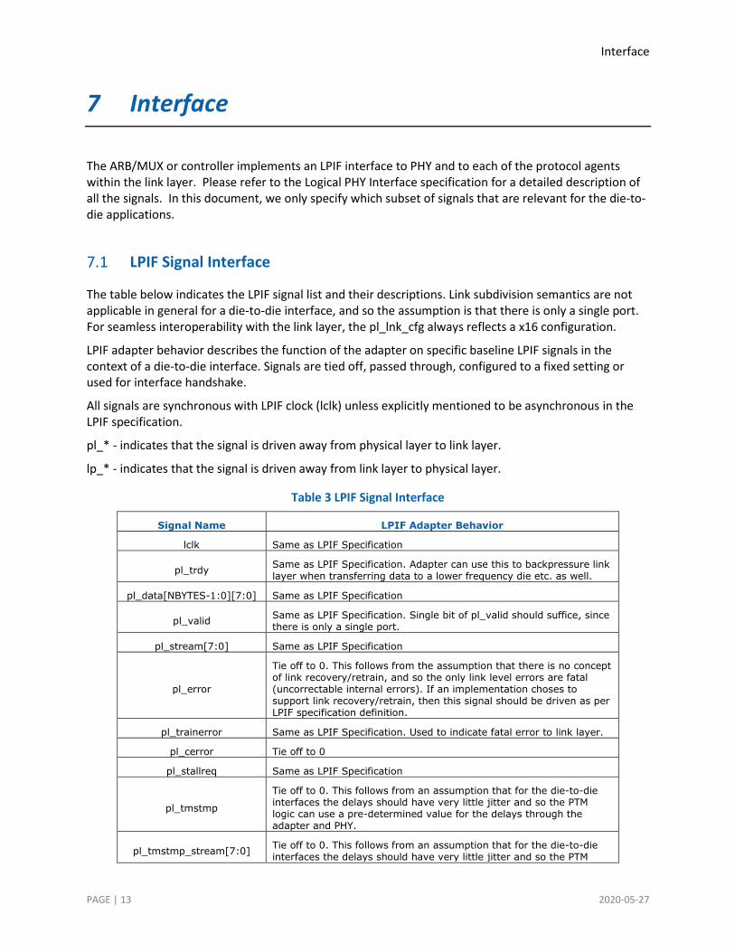
The ARB/MUX or controller implements an LPIF interface to PHY and to each of the protocol agents within the link layer. Please refer to the Logical PHY Interface specification for a detailed description of all the signals. In this document, we only specify which subset of signals that are relevant for the die-to-die applications.
LPIF Signal Interface
The table below indicates the LPIF signal list and their descriptions. Link subdivision semantics are not applicable in general for a die-to-die interface, and so the assumption is that there is only a single port. For seamless interoperability with the link layer, the pl_lnk_cfg always reflects a x16 configuration.
LPIF adapter behavior describes the function of the adapter on specific baseline LPIF signals in the context of a die-to-die interface. Signals are tied off, passed through, configured to a fixed setting or used for interface handshake.
All signals are synchronous with LPIF clock (lclk) unless explicitly mentioned to be asynchronous in the LPIF specification.
pl_* - indicates that the signal is driven away from physical layer to link layer.
lp_* - indicates that the signal is driven away from link layer to physical layer.
Table 3 LPIF Signal Interface
Signal Name LPIF Adapter Behavior
lclk Same as LPIF Specification
pl_trdy Same as LPIF Specification. Adapter can use this to backpressure link layer when transferring data to a lower frequency die etc. as well.
pl_data[NBYTES-1:0][7:0] Same as LPIF Specification
pl_valid Same as LPIF Specification. Single bit of pl_valid should suffice, since there is only a single port.
pl_stream[7:0] Same as LPIF Specification
pl_error
Tie off to 0. This follows from the assumption that there is no concept of link recovery/retrain, and so the only link level errors are fatal (uncorrectable internal errors). If an implementation choses to support link recovery/retrain, then this signal should be driven as per LPIF specification definition.
pl_trainerror Same as LPIF Specification. Used to indicate fatal error to link layer.
pl_cerror Tie off to 0
pl_stallreq Same as LPIF Specification
pl_tmstmp
Tie off to 0. This follows from an assumption that for the die-to-die interfaces the delays should have very little jitter and so the PTM logic can use a pre-determined value for the delays through the adapter and PHY.
pl_tmstmp_stream[7:0] Tie off to 0. This follows from an assumption that for the die-to-die interfaces the delays should have very little jitter and so the PTM

Interface
PAGE | 14 2020-05-27
logic can use a pre-determined value for the delays through the adapter and PHY.
pl_phyinl1 Same as LPIF Specification
pl_phyinl2 Same as LPIF Specification
lp_irdy Same as LPIF Specification
lp_pri[1:0] Tie off to 0
lp_data[NBYTES-1:0][7:0] Same as LPIF Specification
lp_stream[7:0] Same as LPIF Specification
lp_valid Same as LPIF Specification. Single bit should suffice, since there is only one port.
lp_stallack Same as LPIF Specification
lp_state_req[3:0] Same as LPIF Specification. Only supported states.
pl_state_sts[3:0] Same as LPIF Specification. Only supported states.
lp_tmstmp
Tie off to 0. This follows from an assumption that for the die-to-die interfaces the delays should have very little jitter and so the PTM logic can use a pre-determined value for the delays through the adapter and PHY.
lp_linkerror Same as LPIF Specification
pl_quiesce Tie off to 0
lp_flushed_all Tie off to 0
lp_rcvd_crc_err Tie off to 0. This follows from the assumption that there is no requirement of link recovery/retrain for die-to-die transport.
pl_lnk_cfg[2:0] Tie off to code: x16
pl_lnk_up Same as LPIF Specification
pl_rxframe_errmask Tie off to 0
pl_portmode[P-1:0] Tie off to code: x16
pl_portmode_val Tied to 1
pl_speedmode[2:0] Tie off to code: Gen 5 [assuming this is the highest speed supported by the link layer, otherwise tie off to the highest speed supported by the link layer]
pl_clr_lnkeqreq[2:0] Tie off to 0
pl_set_lnkeqreq[2:0] Tie off to 0
pl_inband_pres Tie off to 1
lp_device_present Tie off to 0. Assumption is that this mode is not required for die-to-die transport, and adapter always assumes something is connected to it if it is brought out of reset.
pl_ptm_rx_delay[7:0] Tie off to 0
pl_setlabs Tie off to 0
pl_setlbms Tie off to 0
pl_surprise_lnk_down Tie off to 0: error escalation through train error
pl_protocol[2:0] Tie off to code: CXL [for applications using CXL, it could also be a don’t care if using the adapter in raw mode etc.]
pl_protocol_vld Tied to 1
pl_err_pipestg Tie off to 0

Interface
PAGE | 15 2020-05-27
lp_wake_req Same as LPIF Specification
pl_wake_ack Same as LPIF Specification
pl_clk_req Same as LPIF Specification
lp_clk_ack Same as LPIF Specification
pl_phyinrecenter Handled through STATE_STS=Retrain
pl_exit_cg_req Same as LPIF Specification
pl_exit_cg_ack Same as LPIF Specification
pl_cfg[NC-1:0]
Optional. The assumption being that any configuration registers that
need to be accessed in the LPIF adapter have a SOC specific access mechanism. If that is not present, the LPIF cfg bus can be used for that purpose.
pl_cfg_vld Optional
lp_cfg[NC-1:0] Optional
lp_cfg_vld Optional
Clocking
LPIF clock (lclk) and PHY clock (= 2x lclk in this document) are required for LPIF adapter. Sideband operates at the same data rate as Data. Both lclk and PHY clock are assumed to be generated from the same PLL. This avoids clock crossing FIFOs and reduces latency.

Transaction Flows
PAGE | 16 2020-05-27
8 Transaction Flows
Transactional Interface
This section provides some example flow diagrams to illustrate the handshakes required across each LPIF interface to transition to/from various LSM states. The examples are based on a configuration with two protocol stacks on the main die and companion die.
Boot Flow (RESET to ACTIVE)
Reset to Active (L0) flow is shown in Figure 8. PHY comes out of RESET and trains (indicated by DLL Lock) up to L0. The progression to Active LP state is as shown.
Figure 8 Boot Flow example
RESETLPIF
LPSTATE {ACTIVE}LPSTATE {ACTIVE}
RESET RESET
LPIF
Main LPIF Adapter
CompanionLPIF
CompanionLPIF Adapter
PHYMainLPIF
<ACTIVE_L0>
ACTIVE L0
RESET RESET
First EXIT_CG_REQ/ACK to wake up link layer.
Layer ensures allPM related conditionsare exited first before
ACTIVE STATE request
First EXIT_CG_REQ/ACK to wake up link layer. First EXIT_REQ may not cause ACTIVE state request

Transaction Flows
PAGE | 17 2020-05-27
L1 Entry and Exit example
An example for L1 entry and L1 exit flows are shown in Figure 9 and Figure 10. The PHY may rely on dynamic clock gating for power savings while saving in Active or support going to a low power state (implementation specific). This flow allows the link layers to clock gate themselves when there is no activity and allow other SoC level power management flows to complete. If L1 entry request is rejected the flow example is shown in Figure 11.
The same flow works for L2 entry as well. L2 sideband encoding is used in that case (in cases where sideband is used). L2 exit is usually done through transition to Reset state and performing the ACTIVE handshake requests again.
Figure 9 L1 Entry flow Example
Main LPIF Adapter
CompanionLPIF
CompanionLPIF Adapter
PHY
<ACTIVE_L0>LPIF
LPSTATE {L1.x}LPSTATE {L1.x}
LPSTATE {ACTIVE} LPSTATE {ACTIVE}
LPIF
<ACTIVE_L0>
MainLPIF

Transaction Flows
PAGE | 18 2020-05-27
Figure 10 L1 Exit flow example
<ACTIVE_L0>LPIF
LPSTATE {ACTIVE}
LPSTATE {ACTIVE}
LPSTATE {L1.x} LPSTATE {L1.x}
LPIF
Main LPIF Adapter
CompanionLPIF
CompanionLPIF Adapter
PHY
<ACTIVE_L0>
MainLPIF

Transaction Flows
PAGE | 19 2020-05-27
Figure 11 L1 Entry failure
Main LPIF Adapter
CompanionLPIF
CompanionLPIF Adapter
PHY
<ACTIVE_L0>LPIF
LPSTATE {ACTIVE}
LPSTATE {ACTIVE} LPSTATE {ACTIVE}
LPIF
<ACTIVE_L0>
MainLPIF
Since this interface is ACTIVE, and no request to move to a PM state, STATE_STS can be returned immediately.
STATE_REQ PM PLP needed to initiate STALL_REQ
While waiting for L1 acknowledgement Link Layer decides to abort L1 request
LPSTATE {ACTIVE}
LinkError
A link error flow is shown in Figure 12. Here, a PHY with ECC protection is assumed and the adapter behavior for an uncorrectable error is shown. In cases where the adapter implements ECC, the error could be internally detected by the adapter as well. Similar flow is followed for cases where the link layers detect a fatal error (indicated to the LPIF adapter via lp_linkerror)

Transaction Flows
PAGE | 20 2020-05-27
Figure 12 LinkError behavior example
Main LPIF Adapter
CompanionLPIF
CompanionLPIF Adapter
PHY
<ACTIVE_L0>LPIF
LPSTATE {LinkError}
LPSTATE {ACTIVE} LPSTATE {ACTIVE}
LPIF
RESET
MainLPIF
MDI PHY indicates an ECC error (A low probability un-correctable error).
LPSTATE {LinkError}
ECC error
Adapter drops any packets in flight and transitions to LinkError. Asserts pl_trainerror to show uncorrectable error
Combination of pl_trainerror and STATE_STS=LinkError will map to UIE (un-correctable Internal Error) and escalation path depends on CXL.IO configuration. Exit from this state is only through RESET
LinkReset
The LinkReset flow may be used to propagate reset from Main die to Companion die (analogous to HotReset in PCIe). It is assumed that protocol layer is quiesced before link layer initiates LinkReset flow. Exit from LinkReset requires reset.

Transaction Flows
PAGE | 21 2020-05-27
Figure 13 LinkReset flow
<ACTIVE_L0>LPIF
LPSTATE {LinkReset}
LPSTATE {LinkReset}
LPSTATE {ACTIVE} LPSTATE {ACTIVE}
LPIF
Main LPIF Adapter
CompanionLPIF
CompanionLPIF Adapter
PHY
RESET
MainLPIF