l.pascua.pres
TRANSCRIPT
Leandro E. Pascua
Thin Films Laboratory – Micro and Nanosystems GroupElectronics and Informatics Research CentreNational Institute of Industrial Technology - INTI
National Technological University - UTNBuenos Aires, [email protected]
Fritz Haber Institut der Max Planck Gesellschaft. Berlin. Dezember 2010

1. Introduction
2. Academic background
3. Research experience during my studies at KIT
4. Recent research experience at INTI
5. Expectations and acknowledgments
Fritz Haber Institut der Max Planck Gesellschaft. Berlin. Dezember 2010
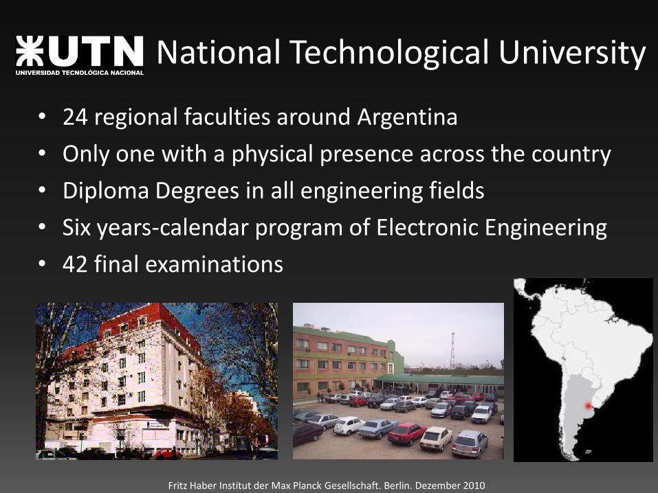
• 24 regional faculties around Argentina
• Only one with a physical presence across the country
• Diploma Degrees in all engineering fields
• Six years-calendar program of Electronic Engineering
• 42 final examinations
Fritz Haber Institut der Max Planck Gesellschaft. Berlin. Dezember 2010
National Technological University
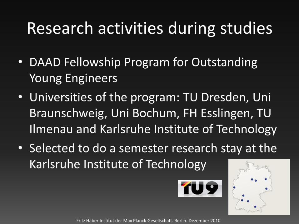
Research activities during studies
• DAAD Fellowship Program for Outstanding Young Engineers
• Universities of the program: TU Dresden, Uni Braunschweig, Uni Bochum, FH Esslingen, TU Ilmenau and Karlsruhe Institute of Technology
• Selected to do a semester research stay at the Karlsruhe Institute of Technology
Fritz Haber Institut der Max Planck Gesellschaft. Berlin. Dezember 2010
Fritz Haber Institut der Max Planck Gesellschaft. Berlin. Dezember 2010
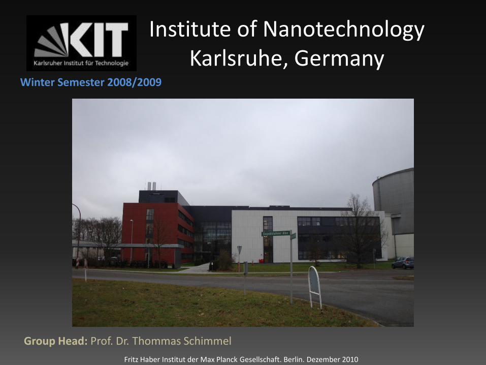
Institute of Nanotechnology Karlsruhe, Germany
Winter Semester 2008/2009
Group Head: Prof. Dr. Thommas Schimmel
Fritz Haber Institut der Max Planck Gesellschaft. Berlin. Dezember 2010
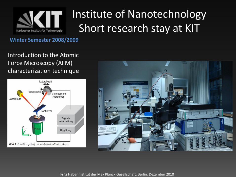
Institute of Nanotechnology Short research stay at KIT
Winter Semester 2008/2009
Introduction to the AtomicForce Microscopy (AFM) characterization technique

Fritz Haber Institut der Max Planck Gesellschaft. Berlin. Dezember 2010
Integration and design of a home-developed systemdedicated to AFM and nanostructuration
Development and improvement of an AFM software dedicated to nanostructured surface patterns. Further developed in C language
Institute of Nanotechnology Short research stay at KIT
Winter Semester 2008/2009
25 nm
Nanostructured sample pattern

Institute of Nanotechnology Short research stay at KIT
Winter Semester 2008/2009
Fritz Haber Institut der Max Planck Gesellschaft. Berlin. Dezember 2010
Example of the developed code in C language for the movement and delay of the AFM tip
Fritz Haber Institut der Max Planck Gesellschaft. Berlin. Dezember 2010
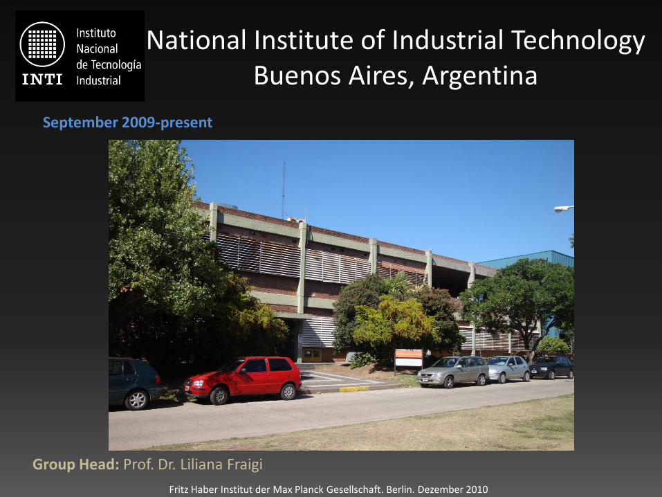
National Institute of Industrial TechnologyBuenos Aires, Argentina
September 2009-present
Group Head: Prof. Dr. Liliana Fraigi

National Institute of Industrial Technology
Fritz Haber Institut der Max Planck Gesellschaft. Berlin. Dezember 2010
Physical Vapor Deposition technique (PVD)for thin films nanostructured materials
RF and DC Magnetron Sputtering at clean room facilities of INTI
Sputtering targets used:•Gold•Chromium•Aluminum•Silicon Dioxide •Vanadium Dioxide•NiCr (80/20) alloy
September 2009-present

National Institute of Industrial Technology
September 2009-present
Fritz Haber Institut der Max Planck Gesellschaft. Berlin. Dezember 2010
Clean room facilities at INTI
72 m2 of clean room
Fritz Haber Institut der Max Planck Gesellschaft. Berlin. Dezember 2010
National Institute of Industrial Technology
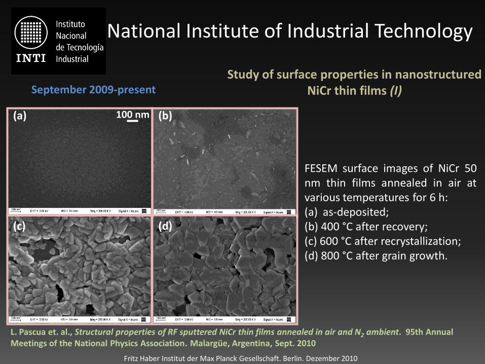
September 2009-presentStudy of surface properties in nanostructured
NiCr thin films (I)
FESEM surface images of NiCr 50nm thin films annealed in air atvarious temperatures for 6 h:(a) as-deposited; (b) 400 °C after recovery; (c) 600 °C after recrystallization; (d) 800 °C after grain growth.
(a) (b)
(c) (d)
L. Pascua et. al., Structural properties of RF sputtered NiCr thin films annealed in air and N2 ambient. 95th Annual Meetings of the National Physics Association. Malargüe, Argentina, Sept. 2010
100 nm
Fritz Haber Institut der Max Planck Gesellschaft. Berlin. Dezember 2010
National Institute of Industrial Technology
September 2009-present
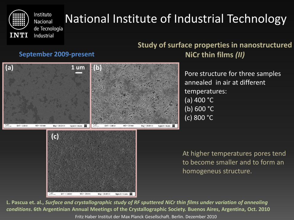
Pore structure for three samples annealed in air at different temperatures:(a) 400 °C (b) 600 °C (c) 800 °C
At higher temperatures pores tendto become smaller and to form an homogeneus structure.
(a) (b)
(c)
Study of surface properties in nanostructured NiCr thin films (II)
1 um
L. Pascua et. al., Surface and crystallographic study of RF sputtered NiCr thin films under variation of annealingconditions. 6th Argentinian Annual Meetings of the Crystallographic Society. Buenos Aires, Argentina, Oct. 2010
Fritz Haber Institut der Max Planck Gesellschaft. Berlin. Dezember 2010
National Institute of Industrial Technology
September 2009-present
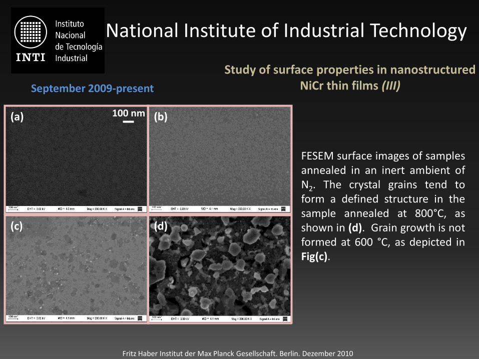
100 nm
FESEM surface images of samplesannealed in an inert ambient ofN2. The crystal grains tend toform a defined structure in thesample annealed at 800°C, asshown in (d). Grain growth is notformed at 600 °C, as depicted inFig(c).
(a) (b)
(c)
(d)
Study of surface properties in nanostructured NiCr thin films (III)
(d)

Fritz Haber Institut der Max Planck Gesellschaft. Berlin. Dezember 2010
National Institute of Industrial Technology
September 2009-present
XRD diffractograms of NiCrthin films annealed in air at various temperatures for 6 hs
The formation of NiO appears when the samples were annealed at 600 and 800°C. either Ni nor Cr peaks were observed. For temperatures below 400°C no NiO is observed. The activation energy is not enough to start the reaction.
Grazing incidence X-ray diffraction
Study of surface properties in nanostructured NiCr thin films (IV)
L. Pascua et. al., FESEM and GIXRD characterization of nanostructured NiCr thin films. At the Frontiers of CondensedMatter V. Buenos Aires, Argentina, Dec. 2010
Fritz Haber Institut der Max Planck Gesellschaft. Berlin. Dezember 2010
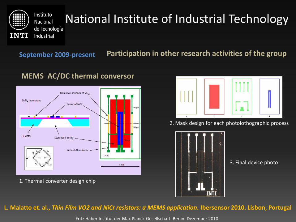
Participation in other research activities of the group
MEMS AC/DC thermal conversor
2. Mask design for each photolothographic process
3. Final device photo
1. Thermal converter design chip
L. Malatto et. al., Thin Film VO2 and NiCr resistors: a MEMS application. Ibersensor 2010. Lisbon, Portugal
National Institute of Industrial Technology
September 2009-present
Fritz Haber Institut der Max Planck Gesellschaft. Berlin. Dezember 2010
National Institute of Industrial Technology
September 2009-present
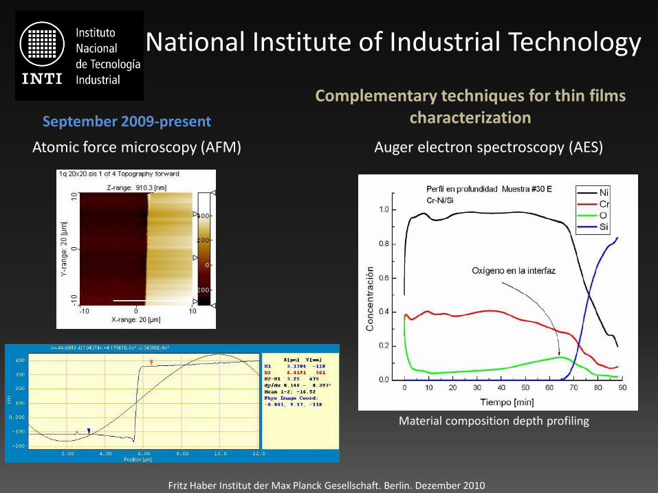
Complementary techniques for thin filmscharacterization
Atomic force microscopy (AFM) Auger electron spectroscopy (AES)
Material composition depth profiling

My expectations …
Fritz Haber Institut der Max Planck Gesellschaft. Berlin. Dezember 2010
Fritz Haber Institut der Max Planck Gesellschaft. Berlin. Dezember 2010
Vielen Dank für Ihre Aufmerksamkeit !!
l l l l l l l l l l l l l l l l l l l l l l l l l l l l l ... goodbye to Nelson Mandela in what will
l l l l l l l l l l l l l l l l l l l l l l ... KIDS PASS: PLANES, TURBO (G) & PERCY JACKSON: SEA OF