low power methodology manual - startseite...low power methodology manual ix 5.5.1 inferring power...
TRANSCRIPT

Low Power Methodology
Manual For System-on-Chip Design

Low Power Methodology Manual For System-on-Chip Design
Robert Aitken Alan Gibbons • Kaijian Shi •Michael Keating • David Flynn •

Michael Keating David Flynn Synopsys, Inc. ARM Limited Palo Alto, CA Cambridge USA United Kingdom
Alan Gibbons Synopsys, Inc. Northampton United Kingdom
Library of Congress Control Number: 2007928355 ISBN 978-0-387-71818-7 e-ISBN 978-0-387-71819-4 Printed on acid-free paper.
rights.
springer.com
All rights reserved. This work may not be translated or copied in whole or in part without the written permission of the publisher (Springer Science+Business Media, LLC, 233 Spring Street, New York, NY 10013, USA), except for brief excerpts in connection with reviews or scholarly analysis. Use in connection with any form of information storage and retrieval, electronic adaptation, computer software, or by similar or dissimilar methodology now known or hereafter developed is forbidden. The use in this publication of trade names, trademarks, service marks and similar terms, even if they are not identified as such, is not to be taken as an expression of opinion as to whether or not they are subject to proprietary
ARM, Inc. Almaden, CA USA
Kaijian Shi Synopsys, Inc. Dallas, TX USA
Robert Aitken
Copyright © 2007 by Synopsys, Inc. & ARM Limited. All rights reserved.
9 8 7 6 5 4 3 2 Corrected at second printing, 2008

TRADEMARKS
Synopsys and NanoSim are registered trademarks of Synopsys, Inc. ARM and AMBA are registered trademarks of ARM Limited. ARM926EJ-S, ARM1176JZF-S, AHB and APB are trademarks of ARM Limited. Artisan and Artisan Components are registered trademarks of ARM Physical IP, Inc.
ARM Limited; and the regional subsidiaries ARM INC.; ARM KK; ARM Korea Ltd.; ARM Taiwan; ARM France SAS; ARM Consulting (Shanghai) Co. Ltd.; ARM Belgium N.V.; AXYS Design Automation Inc.; AXYS GmbH; ARM Embedded Technologies Pvt. Ltd.; and ARM, Inc. and ARM Norway, AS. All other brands or product names are the property of their respective holders.
DISCLAIMER
All content included in this Low Power Methodology Manual is the result of the combined efforts of ARM Limited and Synopsys, Inc. Because of the possibility of human or mechanical error, neither the authors, ARM Limited, Synopsys, Inc., nor any of their affiliates, including but not limited to Springer Science+Business Media, LLC, guarantees the accuracy, adequacy or completeness of any information contained herein and are not responsible for any errors or omissions, or for the results obtained from the use of such information. THERE ARE NO EXPRESS OR IMPLIED WARRANTIES, INCLUDING, BUT NOT LIMITED TO, WARRANTIES OF MERCHANTABILITY OR FITNESS FOR A PARTICULAR PURPOSE relating to the Low Power Methodology Manual. In no event shall the authors, ARM Limited, Synopsys, Inc., or their affiliates be liable for any indirect, special or consequential damages in connection with the information provided herein.
“ARM” is used to represent ARM Holdings plc; its operating company

Table of Contents
Preface...........................................................................................xv
1 Introduction....................................................................................11.1 Overview ....................................................................................................... 11.2 Scope of the Problem..................................................................................... 21.3 Power vs. Energy........................................................................................... 31.4 Dynamic Power ............................................................................................. 41.5 The Conflict Between Dynamic and Static Power ........................................ 71.6 Static Power................................................................................................... 81.7 Purpose of This Book .................................................................................. 10
2 Standard Low Power Methods ...................................................132.1 Clock Gating................................................................................................ 132.2 Gate Level Power Optimization .................................................................. 152.3 Multi VDD................................................................................................... 162.4 Multi-Threshold Logic ................................................................................ 172.5 Summary of the Impact of Standard Low Power Techniques ..................... 19
3 Multi-Voltage Design ...................................................................213.1 Challenges in Multi-Voltage Designs .......................................................... 223.2 Voltage Scaling Interfaces – Level Shifters................................................. 22
3.2.1 Unidirectional Level Shifters ......................................................... 23

viii Low Power Methodology Manual
3.2.23.2.33.2.43.2.5 Automation and Level Shifters....................................................... 273.2.6 Level Shifter Recommendations and Pitfalls ................................. 28
3.3 Timing Issues in Multi-Voltage Designs ..................................................... 293.3.1 Clocks ............................................................................................. 293.3.2 Static Timing Analysis ................................................................... 30
3.4 Power Planning for Multi-Voltage Design .................................................. 303.5 System Design Issues with Multi-Voltage Designs..................................... 31
4 Power Gating Overview ..............................................................334.1 Dynamic and Leakage power profiles......................................................... 334.24.3 Principles of Power Gating Design ............................................................ 37
4.3.1 Power Switching – Fine Grain vs. Coarse Grain............................ 384.3.2 The Challenges of Power Gating.................................................... 39
5 Designing Power Gating..............................................................415.1 Switching Fabric Design ............................................................................. 42
5.1.1 Controlling the Switching Fabric ................................................... 445.1.2
5.25.2.1 Signal Isolation techniques............................................................. 455.2.2 Output or Input Isolation ................................................................ 475.2.3 Interface Protocols and Isolation .................................................... 485.2.4 Recommendations and Pitfalls for Isolation................................... 50
5.35.3.1 State Retention Using Scan Chains ................................................ 515.3.2 Retention Registers......................................................................... 545.3.3 Power Controller Design for Retention.......................................... 565.3.4 Partial vs. Full State Retention ....................................................... 565.3.5 System Level Issues and Retention ................................................ 585.3.6
5.45.4.15.4.2 Handshake Protocols ...................................................................... 615.4.3
5.5
Level Shifters – High to Low Voltage Translation......................... 23Level Shifters – Low-to-High Voltage........................................... 24Level Shifter Placement ................................................................. 25
Impact of Power Gating on Classes of Sub-systems................................... 36
Recommendations and Pitfalls for Power Gating Control ............. 44Signal Isolation .......................................................................................... 45
State Retention and Restoration Methods ................................................... 50
Recommendations and Pitfalls for State Retention ........................ 58Power Gating Control.................................................................................. 59
Power Control Sequencing.............................................................. 60
Recommendations and Pitfalls for Power Gating Controllers ....... 63Power Gating Design Verification – RTL Simulation................................. 63

Low Power Methodology Manual ix
5.5.1 Inferring Power Gating Behavior in RTL....................................... 645.5.2 Inferring Power Gating and Retention Behavior in RTL ............... 68
5.6 Design For Test considerations ................................................................... 705.6.1 Power Gating Controls ................................................................... 705.6.2 Power Limitations during Scan Test............................................... 715.6.3 Testing the Switching Network ...................................................... 715.6.4 Testing Isolation and Retention ...................................................... 725.6.5 Testing the Power Gating Controller .............................................. 73
6 Architectural Issues for Power Gating ......................................756.1 Hierarchy and Power Gating ....................................................................... 756.2
6.2.16.2.2
6.3 Power State Tables and Always On Regions............................................... 82
7 A Power Gating Example............................................................857.17.2 Design partitioning ...................................................................................... 887.3 Isolation ....................................................................................................... 927.4 Retention...................................................................................................... 947.5 Inferring Power Gating and Retention ....................................................... 957.6 Measurements and Analysis ........................................................................ 96
8 IP Design for Low Power ..........................................................1018.1 Architecture and Partitioning for Power Gating........................................ 102
8.1.1 How and When to Shut Down...................................................... 1038.1.2
8.2 Power Controller Design for the USB OTG.............................................. 1058.3 Issues in Designing Portable Power Controllers ....................................... 1088.4 Clocks and Resets ..................................................................................... 1098.5 Verification ................................................................................................ 1098.6 Packaging IP for Reuse with Power Intent.................................................1108.7 UPF for the USB OTG Core ......................................................................1118.8 USB OTG Power Gating Controller State Machine...................................114
Power Networks and Their Control............................................................. 78
On-chip Power Gating .................................................................... 81External Power Rail Switching....................................................... 79
Leakage Modes Supported .......................................................................... 85
What to Shut Down and What to Keep Alive .............................. 103

x Low Power Methodology Manual
9 Frequency and Voltage Scaling Design ....................................1219.1 Dynamic Power and Energy ...................................................................... 1229.2 Voltage Scaling Approaches...................................................................... 1259.3 Dynamic Voltage and Frequency Scaling (DVFS).................................... 1259.4 CPU Subsystem Design Issues.................................................................. 1299.5 Adaptive Voltage Scaling (AVS) ............................................................... 1309.6 Level Shifters and Isolation....................................................................... 1319.7 Voltage Scaling Interfaces – Effect on Synchronous Timing .................... 1329.8
10 Examples of Voltage and Frequency Scaling Design ............13910.1 Voltage Scaling - A Worked Example for UMC 130nm ........................... 139
10.1.1 ULTRA926 System Design Block Diagram ................................ 14010.1.210.1.3 Synchronous Design Constraints.................................................. 14410.1.4 Simulated (predicted) Energy Savings Analysis .......................... 14510.1.510.1.6
10.2.110.2.210.2.3
11 Implementing Multi-Voltage, Power Gated Designs.............15511.1 Design Partitioning.................................................................................... 158
11.1.1 Logical and Physical Hierarchy.................................................... 15811.1.2 Critical Path Timing ..................................................................... 160
11.2 Design Flow Overview.............................................................................. 16011.3 Synthesis.................................................................................................... 162
11.3.1 Power Intent ................................................................................. 16211.3.2 Defining Power Domains and Power Connectivity...................... 16211.3.3 Isolation Cell Insertion ................................................................. 16311.3.4 Retention Register Insertion ......................................................... 16411.3.5 Level Shifter Insertion.................................................................. 16611.3.6 Scan Synthesis .............................................................................. 16811.3.7 Always-On Network Synthesis .................................................... 170
11.4 Multi Corner Multi Mode Optimization with Voltage Scaling Designs.... 17111.5 Design Planning......................................................................................... 173
Control of Voltage Scaling ......................................................................... 136
Voltage/Frequency Range Exploration......................................... 141
Silicon-Measured Power and Performance Analysis................... 145Silicon-Measured ULTRA926 DVFS Energy Savings Analysis .. 147
10.2 Voltage Scaling – A worked Example for TSMC 65nm........................... 150
Voltage/Frequency Range Exploration......................................... 151Silicon-Measured Power and Performance Analysis.................... 151
ATLAS926 Case Study ................................................................. 150

Low Power Methodology Manual xi
11.5.1 Creating Voltage Areas................................................................. 17311.5.2 Power Gating Topologies ............................................................. 17511.5.3 In-rush Current Management ....................................................... 17611.5.4 Recommendations: ....................................................................... 176
11.6 Power Planning.......................................................................................... 17711.6.1 Decoupling Capacitor Insertion.................................................... 179
11.7 Clock Tree Synthesis ................................................................................. 18011.8 Power Analysis.......................................................................................... 18311.9 Timing Analysis ........................................................................................ 18411.10Low Power Validation............................................................................... 18511.11Manufacturing Test.................................................................................... 185
12 Physical Libraries ....................................................................18712.1 Standard Cell Libraries.............................................................................. 187
12.1.1 Modeling of Standard Cell Libraries ............................................ 18812.1.2 Characterization of Standard Cell Libraries ................................. 189
12.2 Special Cells - Isolation Cells.................................................................... 19012.2.112.2.2 Output Isolation vs. Input Isolation ............................................. 19312.2.312.2.4 Recommendations ........................................................................ 194
12.3 Special Cells - Level Shifters .................................................................... 19512.4 Memories................................................................................................... 198
12.4.1 RAMs for Multi-Voltage Power Gated Designs........................... 19912.4.2 Memories and Retention............................................................... 200
12.5 Power Gating Strategies and Structures .................................................... 20012.5.1 Power Gating Structures............................................................... 20112.5.2 Recommendations – Coarse Grain vs. Fine Grain ....................... 204
12.6 Power Gating Cells.................................................................................... 204
13 Retention Register Design .......................................................20913.1 Retention Registers.................................................................................... 209
13.1.1 Single Pin “Live Slave” Retention Registers ............................... 20913.1.213.1.313.1.4 Retention Register: Relative layout.............................................. 218
13.2.1
Signal Isolation............................................................................. 191
Sneak DC Leakage Paths .............................................................. 193
12.7 Power Gated Standard Cell Libraries ........................................................ 206
Dual Control Signal “Balloon” Retention Register ..................... 212Single Control Signal “Balloon” Retention Register.................... 215
13.2 Memory Retention Methods....................................................................... 219VDD Retention Method ................................................................. 219

xii Low Power Methodology Manual
13.2.213.2.313.2.4
14 Design of the Power Switching Network................................22514.1 Ring vs. Grid Style ................................................................................... 225
14.1.114.1.214.1.3 Row and Column Grids ................................................................ 22914.1.414.1.5 Recommendations - Ring vs. Grid Style ..................................... 231
14.2 Header vs. Footer Switch .......................................................................... 23214.2.114.2.214.2.314.2.414.2.5
14.3.114.3.214.3.3 Recommendations for Supply Distribution .................................. 239
14.4 A Sleep Transistor Example ...................................................................... 23914.5 Wakeup Current and Latency Control Methods ........................................ 240
14.5.114.5.214.5.314.5.414.5.514.5.614.5.714.5.8 Recommendations for Power Switching Control ......................... 245
14.6 An Example of a Dual Daisy Chain Sleep Transistor Implementation..... 246
APPENDIX A Sleep Transistor Design.......................................249A.1
A.1.1A.1.2A.1.3A.1.4
Retention Latency Reduction Methods ........................................ 222Source Biasing Method ................................................................. 221Source-diode Biasing Method ...................................................... 219
Ring Style Implementation........................................................... 226Grid Style Implementation ........................................................... 227
Hybrid Style Implementation ........................................................ 231
Switch Efficiency Considerations ................................................. 232
Recommendations – Header vs. Footer........................................ 235System Level Design Consideration.............................................. 235
Area Efficiency Consideration and L/W Choice .......................... 234Body Bias Considerations............................................................. 235
Single Daisy chain sleep transistor distribution ........................... 241Dual Daisy chain sleep transistor distribution............................... 241
Main Chain Turn-on Control ....................................................... 243Buffer Delay Based Main Chain Turn-on Control ...................... 243
Parallel Short Chain Distribution of the Main Sleep Transistor ... 243
Power-off Latency Reduction ....................................................... 244Programmable Main Chain Turn-on Control................................ 244
Sleep Transistor Design Metrics ................................................................ 250Switch Efficiency .......................................................................... 250Area Efficiency .............................................................................. 253IR Drop.......................................................................................... 253Normal vs. Reverse Body Bias ..................................................... 254
14.3 Rail vs. Strap VDD Supply ........................................................................ 236Parallel Rail VDD Distribution .................................................... 236Power Strap VDD Distribution ..................................................... 238

Low Power Methodology Manual xiii
A.1.5 Recommendations ........................................................................ 259A.2
A.2.1 Recommendations ........................................................................ 262A.3
A.3.1 Recommendations ........................................................................ 263A.4
APPENDIX B UPF Command Syntax........................................267B.1 add_pst_state ............................................................................................ 268B.2 connect_supply_net .................................................................................. 269B.3 create_power_domain ............................................................................... 271B.4 create_power_switch ................................................................................ 273B.5 create_pst .................................................................................................. 275B.6 create_supply_net ..................................................................................... 276B.7 create_supply_port ................................................................................... 277B.8 set_domain_supply_net ............................................................................ 278B.9 set_isolation .............................................................................................. 279B.10 set_isolation_control ................................................................................. 281B.11 set_level_shifter ........................................................................................ 283B.12 set_retention ............................................................................................. 285B.13 set_retention_control ................................................................................ 287B.14 set_scope ................................................................................................... 288
Glossary ......................................................................................291
Bibliography ...............................................................................293
Index ...........................................................................................297
Layout Design for Area Efficiency .......................................................... 260
Single Row vs. Double Row...................................................................... 262
In-rush Current and Latency Analysis ........................................................ 263
Preface
FIGURE 1.0.TABLE 1.0.
The Low Power Methodology Manual is the outcome of a decade-long collaborationbetween ARM and Synopsys commercially and the two of us personally. In 1997ARM and Synopsys worked together to develop a synthesizable ARM7 core. Davewas the ARM lead on the project; Mike’s team executed the Synopsys side of theproject. This led to a similar project on the ARM9.
Shortly after these projects, the two of us embarked on a series of technology demon-stration projects. We both felt that we needed to use our products as our customers doin order to understand how to make these products better. So we developed a test chipthat combined ARM and Synopsys IP and took it through to silicon. We did the RTLdesign and verification personally, and borrowed resources to do the implementation.The experience was incredibly illuminating, and we hope it contributed to improvingthe IP and tools from both companies.
We quickly realized that low power was one of the key concerns of our customers,and SoC designers in general. So we followed our initial project with several lowpower technology demonstration projects. The final project was the SALT (SynopsysARM Low-power Technology demonstrator) project, for which we received workingsilicon late last year. These projects explored clock gating, multi-voltage, dynamicvoltage scaling, and power gating. In all these projects we found that there is no sub-stitute for direct first-hand experience doing low-power IP-based designs. We learned,in the most concrete way possible, exactly what our customers go through on an SoCdesign.
For years we have been talking about writing a book on low power design. With ourexperience on the SALT project, our work with customers on low power designs, and

xvi Low Power Methodology Manual
our participation in developing the UPF low-power standard, we feel that we arefinally in a position to publish our insights and perspectives.
In doing so, we have enlisted the aid of our co-authors. The two of us are primarilyfront-end engineers, with a background in system architecture and RTL design.Kaijian and Rob bring a great depth of technical expertise in the physical and circuitdesign aspects of low power. Alan has developed low power flows for the ARM pro-cessors and did the implementation of SALT. As a result, he brings a unique perspec-tive on the implementation issues in low power design.
We cannot overstate the contribution of our co-authors. Without their insights andexpertise - as well as the material they contributed directly - this book could not havebeen written.
Like all our joint projects, this book was partly a formal joint project of the two com-panies and partly (perhaps mostly) driven by the personal commitment of the authors,aided and abetted by many others. We got considerable help from many people forwhom this was not part of their job description. These kind souls took time out oftheir busy schedules, including evenings and weekends, to help us at every step of ourjourney, from the first joint chip development to the completion of this book. Theyhelped in the architecture, design and tape out of test chips, the building and debug-ging of boards, and the review and editing of the final manuscript.
It is impossible to list them all, but we list some of the many who contributed to thiseffort: Anwar Awad, John Biggs, Pin-Hung Chen, Sachin Rai, David Howard, andSachin Idgunji.
We would also like to thank the staffs of TSMC and UMC for fabricating the technol-ogy demonstrators and enabling us to derive the results referenced in the workedexamples.
Dave Flynn Mike KeatingCambridge, UK Palo Alto, CA

CHAPTER 1 IntroductionFIGURE 2.0.TABLE 2.0.EXAMPLE 1.0.
1.1 OverviewThe design of complex chips has undergone a series of revolutions during the lasttwenty years. In the 1980s there was the introduction of language-based design andsynthesis. In the 1990s, there was the adoption of design reuse and IP as a mainstreamdesign practice. In the last few years, design for low power has started to changeagain how designers approach complex SoC designs.
Each of these revolutions has been a response to the challenges posed by evolvingsemiconductor technology. The exponential increase in chip density drove the adop-tion of language-based design and synthesis, providing a dramatic increase in
in the era of million gate designs, engineers discovered that there was a limit to howmuch new RTL could be written for a new chip project. The result was that IP anddesign reuse became accepted as the only practical way to design large chips with rel-atively small design teams. Today every SoC design employs substantial IP in orderto take advantage of the ever increasing density offered by sub-micron technology.
Deep submicron technology, from 130nm on, poses a new set of design problems. Wecan now implement tens of millions of gates on a reasonably small die, leading to apower density and total power dissipation that is at the limits of what packaging, cool-ing, and other infrastructure can support. As technology has shrunk to 90nm andbelow, the leakage current is increasing dramatically, to the point where, in some65nm designs, leakage current is nearly as large as dynamic current.
These changes are having a significant effect on how chips are designed. The powerdensity of the highest performance chips has grown to the point where it is no longer
designer productivity. This approach held Moore’s law at bay for a decade or so, but

2 Low Power Methodology Manual
possible to increase clock speed as technology shrinks. As a result, designers aredesigning multi-processor chips instead of chips with a single, ultra-high speed pro-cessor.
For battery-powered devices, which comprise one of the fastest growing segments ofthe electronics market, the leakage of deep submicron processes is a major problem.
approaches include power gating, where blocks are powered down when not in use,and multi-threshold libraries that can trade-off leakage current for speed.
For all applications, the total power consumption of complex SoCs presents a chal-lenge. To address this challenge, designers are moving from a monolithic approachfor power the chip—where a single supply voltage is used for all the non-IO gates ofthe design—to a multiple supply architecture, where different blocks are run at differ-ent voltages, depending on their individual requirements. And in some cases, design-ers are using voltage scaling techniques to change the supply voltage (and clockfrequency) to a critical block depending on its workload and hence required perfor-mance.
This book describes a number of the techniques designers can use to reduce the powerconsumption of complex SoC designs. Our approach is practical, rather than theoreti-cal. We draw heavily upon the experience we have gained in doing a series of technol-ogy demonstrator chips over the last several years. We believe the techniques wedescribe can be used today by chip designers to improve significantly the chips theydesign.
1.2 Scope of the ProblemToday some of the most powerful microprocessor chips can dissipate 100-150 Watts,for an average power density of 50-75 Watts per square centimeter. Local hot spots onthe die can be several times higher than this number.
This power density not only presents packaging and cooling challenges; it also canpose problems for reliability, since the mean time to failure decreases exponentiallywith temperature. In addition, timing degrades with temperature and leakageincreases with temperature.
Historically, the power in the highest performance chips has increased with each newtechnology node. But because of the issues posed by the power density, the Interna-tional Technology Roadmap for Semiconductors (ITRS) predicts that the power forthese chips will reach a maximum of 198 Watts in 2008; after that, power will remainconstant.
of the design process, from software to architecture to implementation. TheseTo combat this problem, designers are using aggressive approaches at every step

Introduction 3
Already, the total power consumption of microprocessor chips presents a significantproblem for server farms. For these server farms, infrastructure costs (power, cooling)can equal the cost of the computers themselves.
For battery-powered, hand-held devices, the numbers are smaller but the problem justas serious. According to ITRS, battery life for these devices peaked in 2004. Sincethen, battery life has declined as features have been added faster than power (per fea-ture) has been reduced.
For virtually all applications, reducing the power consumed by SoCs is essential inorder to continue to add performance and features and grow these businesses.
Until recently, power has been a second order concern in chip design, following firstorder issues such as cost, area, and timing. Today, for most SoC designs, the powerbudget is one of the most important design goals of the project. Exceeding the powerbudget can be fatal to a project, whether it means moving from a cheap plastic pack-age to an expensive ceramic one, or causing an unacceptably poor reliability due toexcessive power density, or failing to meeting the required battery life.
These problems are all expected to get worse as we move to the next technologynodes. The ITRS makes the following predictions:
Needless to say, many design teams are working very hard to reduce the growth inpower below these forecast numbers, since even at 90nm many designs are at thelimit of what their customers will accept.
1.3 Power vs. EnergyFor battery operated devices, the distinction between power and energy is critical.Figure 1-1 on page 4 illustrates the difference. Power is the instantaneous power inthe device. Energy is the area under the curve—the integral of power over time. Thepower used by a cell phone, for example, varies depending on the what it is doing—
Table 1-1
Node 90nm 65nm 45nm
Dynamic Power per cm2 1X 1.4X 2X
Static Power per cm2 1X 2.5X 6.5X
Total Power per cm2 1X 2X 4X

4 Low Power Methodology Manual
whether it is in standby with the cover closed, or open and the display is powered up,or downloading from the web. The height of the graph in Figure 1-1 shows the power,but it is energy—the area under the curve—that determines battery life.
Figure 1-1 Power vs. Energy
1.4 Dynamic Power
The total power for an SoC design consists of dynamic power and static power.Dynamic power is the power consumed when the device is active—that is, when sig-nals are changing values. Static power is the power consumed when the device ispowered up but no signals are changing value. In CMOS devices, static power con-sumption is due to leakage.
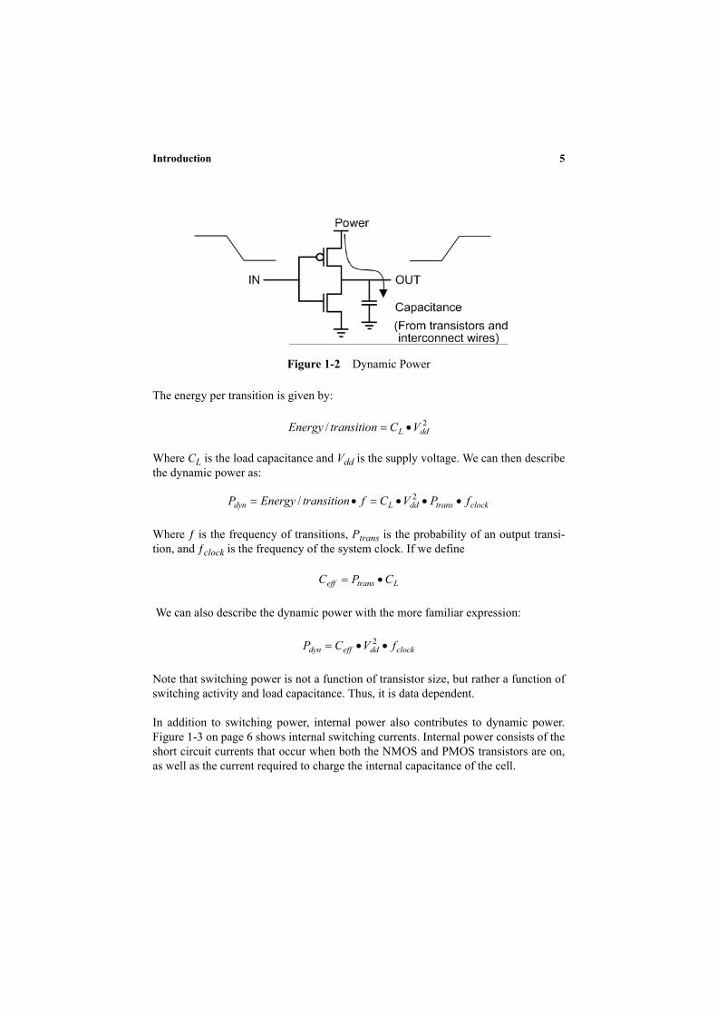
The first and primary source of dynamic power consumption is switching power—thepower required to charge and discharge the output capacitance on a gate. Figure 1-2on page 5 illustrates switching power.
Introduction 5
Figure 1-2 Dynamic Power
The energy per transition is given by:
Where CL is the load capacitance and Vdd is the supply voltage. We can then describethe dynamic power as:
Where ƒ is the frequency of transitions, Ptrans is the probability of an output transi-tion, and ƒclock is the frequency of the system clock. If we define
We can also describe the dynamic power with the more familiar expression:
Note that switching power is not a function of transistor size, but rather a function ofswitching activity and load capacitance. Thus, it is data dependent.
In addition to switching power, internal power also contributes to dynamic power.Figure 1-3 on page 6 shows internal switching currents. Internal power consists of theshort circuit currents that occur when both the NMOS and PMOS transistors are on,as well as the current required to charge the internal capacitance of the cell.
2/ ddL VCtransitionEnergy •=
clocktransddLdyn fPVCftransitionEnergyP •••=•= 2/
Ltranseff CPC •=
clockddeffdyn fVCP ••= 2

6 Low Power Methodology Manual
Figure 1-3 Crowbar Current
If we add the expression for internal power to our equation, we can describe thedynamic power as:
Where tsc is the time duration of the short circuit current, and Ipeak is the total internalswitching current (short circuit current plus the current required to charge the internalcapacitance).
As long as the ramp time of the input signal is kept short, the short circuit currentoccurs for only a short time during each transition, and the overall dynamic power isdominated by the switching power. For this reason, we often simplify the use theswitching power formula
But there are occasions when the short circuit current (often called crowbar current) isof interest. In particular, we will discuss ways of preventing excess crowbar currentwhen we talk about how to deal with the floating outputs of a power gated block.
There are a number of techniques at the architectural, logic design, and circuit designthat can reduce the power for a particular function implemented in a given technol-ogy. These techniques focus on the voltage and frequency components of the equa-tion, as well as reducing the data-dependent switching activity.
There are a variety of architectural and logic design techniques for minimizingswitching activity, which effectively lowers switching activity for the gates involved.An interesting example is [1], which describes how engineers have used micro-archi-tecture modifications to reduce power significantly in Intel processors.
( ) ( )clockpeakddscclockddeffdyn fIVtfVCP •••+••= 2
clockddeffdyn fVCP ••= 2
Introduction 7
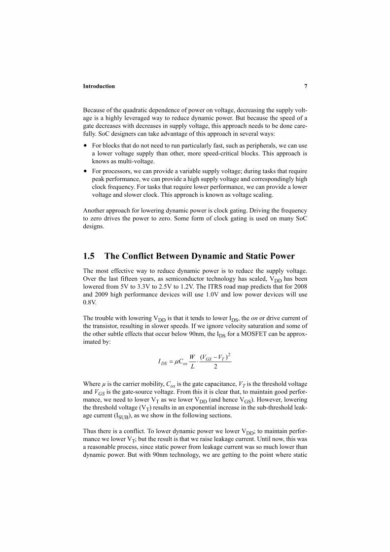
Because of the quadratic dependence of power on voltage, decreasing the supply volt-age is a highly leveraged way to reduce dynamic power. But because the speed of agate decreases with decreases in supply voltage, this approach needs to be done care-fully. SoC designers can take advantage of this approach in several ways:
• For blocks that do not need to run particularly fast, such as peripherals, we can usea lower voltage supply than other, more speed-critical blocks. This approach isknows as multi-voltage.
• For processors, we can provide a variable supply voltage; during tasks that requirepeak performance, we can provide a high supply voltage and correspondingly highclock frequency. For tasks that require lower performance, we can provide a lowervoltage and slower clock. This approach is known as voltage scaling.
Another approach for lowering dynamic power is clock gating. Driving the frequencyto zero drives the power to zero. Some form of clock gating is used on many SoCdesigns.
1.5 The Conflict Between Dynamic and Static PowerThe most effective way to reduce dynamic power is to reduce the supply voltage.Over the last fifteen years, as semiconductor technology has scaled, VDD has beenlowered from 5V to 3.3V to 2.5V to 1.2V. The ITRS road map predicts that for 2008and 2009 high performance devices will use 1.0V and low power devices will use0.8V.
The trouble with lowering VDD is that it tends to lower IDS, the on or drive current ofthe transistor, resulting in slower speeds. If we ignore velocity saturation and some ofthe other subtle effects that occur below 90nm, the IDS for a MOSFET can be approx-imated by:
Where µ is the carrier mobility, Cox is the gate capacitance, VT is the threshold voltageand VGS is the gate-source voltage. From this it is clear that, to maintain good perfor-mance, we need to lower VT as we lower VDD (and hence VGS). However, loweringthe threshold voltage (VT) results in an exponential increase in the sub-threshold leak-age current (ISUB), as we show in the following sections.
Thus there is a conflict. To lower dynamic power we lower VDD; to maintain perfor-mance we lower VT; but the result is that we raise leakage current. Until now, this wasa reasonable process, since static power from leakage current was so much lower thandynamic power. But with 90nm technology, we are getting to the point where static
2)( 2
TGSoxDS
VVL
WCI −⋅= μ

8 Low Power Methodology Manual
power can be as big a problem as dynamic power, and we need to examine this con-flict more carefully.
1.6 Static Power
There are four main sources of leakage currents in a CMOS gate (Figure 1-4)
• Sub-threshold Leakage (ISUB): the current which flows from the drain to thesource current of a transistor operating in the weak inversion region.
• Gate Leakage (IGATE): the current which flows directly from the gate through theoxide to the substrate due to gate oxide tunneling and hot carrier injection.
• Gate Induced Drain Leakage (IGIDL): the current which flows from the drain to thesubstrate induced by a high field effect in the MOSFET drain caused by a highVDG.
• Reverse Bias Junction Leakage (IREV): caused by minority carrier drift and gener-ation of electron/hole pairs in the depletion regions.
Figure 1-4 Leakage Currents
Sub-threshold leakage occurs when a CMOS gate is not turned completely off. To agood approximation, its value is given by
Where W and L are the dimensions of the transistor, and Vth is the thermal voltagekT/q (25.9mV at room temperature). The parameter n is a function of the device fab-rication process and ranges from 1.0 to 2.5.
⋅⋅=−
th
TGSnV
VV
thoxSUB eL
WVCI 2μ

Introduction 9
This equation tells us that sub-threshold leakage depends exponentially on the differ-ence between VGS and VT. So as we scale VDD and VT down (to limit dynamicpower) we make leakage power exponentially worse.
Gate leakage occurs as a result of tunneling current through the gate oxide. The gateoxide thickness (TOX) is only a few atoms thick in 90nm gates—this is so thin thattunneling current can become substantial. In previous technology nodes, leakage cur-rent has been dominated by sub-threshold leakage. But starting with 90nm, gate leak-age can be nearly 1/3 as much as sub-threshold leakage. In 65nm it can equal sub-threshold leakage in some cases. At future nodes, high-k dielectric materials will berequired to keep gate leakage in check. This appears to be the only effective way ofreducing gate leakage.
Sub-threshold leakage current increases exponentially with temperature. This greatlycomplicates the problem of designing low power systems. Even if the leakage at roomtemperature is acceptable, at worst case temperature it can exceed the design goals ofthe chip.
There are several approaches to minimizing leakage current.
One technique is known as Multi-VT: using high VT cells wherever performancegoals allow and low VT cells where necessary to meet timing.
A second technique is to shut down the power supply to a block of logic when it is notactive. This approach is known as power gating.
These two approaches are discussed in more detail in later chapters. For now, though,we mention three other techniques:
VTCMOSVariable Threshold CMOS (VTCMOS) is another very effective way of miti-gating standby leakage power. By applying a reverse bias voltage to the sub-strate, it is possible to reduce the value of the term (VGS-VT), effectivelyincreasing VT. This approach can reduce the standby leakage by up to threeorders of magnitude. However, VTCMOS adds complexity to the library andrequires two additional power networks to separately control the voltageapplied to the wells. Unfortunately, the effectiveness of reverse body bias hasbeen shown to be decreasing with scaling technology [2].
Stack EffectThe Stack Effect, or self reverse bias, can help to reduce sub-threshold leakagewhen more than one transistor in the stack is turned off. This is primarilybecause the small amount of sub-threshold leakage causes the intermediatenodes between the stacked transistors to float away from the power/groundrail. The reduced body-source potential results in a slightly negative gate-source drain voltage. Thus, it reduces the value of the term (VGS-VT), effec-

10 Low Power Methodology Manual
tively increasing VT and reducing the sub-threshold leakage. The leakage of a
two transistor stack has been shown to be an order of magnitude less than that
of a single transistor [3]. This stacking effect makes the leakage of a logic gate
highly dependent on its inputs. There is a minimum leakage state for any
multi-input circuit; in theory this state applied just prior to halting the clocks to
minimize leakage. In practice, applying this state is not feasible in most
designs.
Long Channel Devices
From the equation for sub-threshold current, it is clear that using non-mini-
mum length channels will reduce leakage. Unfortunately, long channel
devices have lower dynamic current, degrading performance. They are also
larger and therefore have greater gate capacitance, which has an adverse effect
on dynamic power consumption and further degrades performance. There may
not be a reduction in total power dissipation unless the switching activity of
the long channel devices is low. Therefore, switching activity and perfor-
mance goals must be taken in to account when using long channel devices.
1.7 Purpose of This Book
The purpose of the Low Power Methodology Manual is to describe the most effective
new techniques for managing dynamic and static power in SoC designs. We describe
the decisions that engineers need to make in designing low power chips, and provide
the information they need to make good decisions. Based on our experience with real
chip designs and a set of silicon technology demonstrators, we provide a set of recom-
mendations and describe common pitfalls in doing low power design.
The process of designing a complex chip is itself very complex, involving many
stakeholders and participants: systems engineers, RTL designers, IP designers, physi-
cal implementation engineers, verification engineers, and library developers. Com-
munication between these disparate players is always a challenge. Each group has its
own area of focus, its own priorities, and often its own language. One goal of this
book is to give these groups a common language for discussing low power design and
a common understanding of the issues involved in implementing a low power strat-
egy.
The first low power decision an SoC design team must make, of course, is what
power strategy to pursue—what techniques to use, when and where and on what sec-
tion of the chip. This fundamental issue drives the structure of the book.

Introduction 11
• Chapter 1 (this chapter) gives and over view of the challenges and basic approachto low power design.
• Chapter 2 discusses clock gating methods, Multi-VT designs, logic-level powerreduction techniques, and multi-voltage design.
• Chapter 3 gives a more detailed description of multi-voltage design, focusing onarchitecture and design issues.
• Chapter 4 gives an overview of power gating• Chapter 5 addresses design aspects of power gating at the RTL level• Chapter 6 provides an example of a power gated chip design at the RTL level• Chapter 7 discusses architectural issues in power gating.• Chapter 8 discusses issues in IP design for power gating, including an example.• Chapter 9 discusses architectural and RTL level design issues in dynamic voltage
and frequency scaling.• Chapter 10 discusses some examples of voltage and frequency scaling • Chapter 11 discusses implementation issues in low power design: synthesis, place
and route, timing analysis and power analysis• Chapter 12 discusses standard cell library and memory requirements for power
gating.• Chapter 13 discusses retention register design and data retention in memories• Chapter 14 discusses the design of the power switching network• Appendix A provides some additional information on the circuit design of sleep
transistors and power switch networks.• Appendix B provides detailed descriptions of the UPF commands used in the text.
Throughout the book, we will make reference to several low power technology dem-onstration projects that the authors have used to explore low power techniques. Theseprojects include:
The SALT project (Synopsys ARM Low power Technology demonstrator) is a 90nmdesign consisting of an ARM processor and numerous Synopsys peripheral and IO IP.This project focused primarily on power gating techniques. Both the processor andthe USB OTG core are power gated.
References
1. Baron, M., “Energy-Efficient Performance at Intel”, Microprocessor Report,December 11, 2006.
2. Neau, C. and Roy, K. “Optimal Body Bias Selection for Leakage Improvementand Process Compensation over Different Technology Generations,” Proceedingsof the ISLPED, 2003

12 Low Power Methodology Manual
3. S. Narendra et al. “Scaling of Stack Effect and its Application for Leakage Reduc-tion”, Int. Symp. on Low Power Electronics and Designs, pp.195-200, 2001

CHAPTER 2 Standard Low Power Methods
FIGURE 2.0.TABLE 2.0.
There are a number of power reduction methods that have been used for some time,and which are mature technologies. This chapter describes some of these approachesto low power design.:
• Clock Gating• Gate Level Power Optimization• Multi-VDD• Multi-VT
2.1 Clock Gating
A significant fraction of the dynamic power in a chip is in the distribution network ofthe clock. Up to 50% or even more of the dynamic power can be spent in the clockbuffers. This result makes intuitive sense since these buffers have the highest togglerate in the system, there are lots of them, and they often have a high drive strength tominimize clock delay. In addition, the flops receiving the clock dissipate somedynamic power even if the input and output remain the same.
The most common way to reduce this power is to turn clocks off when they are notrequired. This approach is known as clock gating.
Modern design tools support automatic clock gating: they can identify circuits whereclock gating can be inserted without changing the function of the logic. Figure 2-1shows how this works.

14 Low Power Methodology Manual
Figure 2-1 Clock Gating
In the original RTL, the register is updated or not depending on a variable (EN). Thesame result can be achieve by gating the clock based on the same variable.
If the registers involved are single bits, then a small savings occurs. If they are, say,32 bit registers, then one clock gating cell can gate the clock to all 32 registers (andany buffers in their clock trees). This can result in considerable power savings.
In the early days of RTL design, engineers would code clock gating circuits explicitlyin the RTL. This approach is error prone – it is very easy to create a clock gating cir-cuit that glitches during gating, producing functional errors. Today, most librariesinclude specific clock gating cells that are recognized by the synthesis tool. The com-bination of explicit clock gating cells and automatic insertion makes clock gating asimple and reliable way of reducing power. No change to the RTL is required toimplement this style of clock gating.
Results
In a recent paper [1], Pokhrel reports on a unique opportunity his team recently had tocompare a (nearly) identical chip implemented both with and without clock gating.As a power reduction project, an existing 180nm chip without clock gating was re-
EN
QD
CLK
always@ (posedge CLK) if (EN) Q <= D;
Typical compile
D Q
gclk
Compile with clock gating
insertion
Low activity
High activity
EN
CLK

Standard Low Power Methods 15
implemented in the same technology with clock gating. Only minor changes in thelogic were implemented (some small blocks were removed and replaced by otherblocks, for a small net increase in functionality).
Pokhrel reports an area reduction of 20% and a power savings of 34% to 43%,depending on the operating mode. (This savings was realized on the clock gated partof the chip; the processor was a hard macro and not clock gated. Power measurementswere made on the whole chip when the processor was in IDLE mode; that is, the pro-cessor was turned off.) The power measurements are from actual silicon.
The area savings is due to the fact that a single clock gating cell takes the place ofmultiple muxes.
Pokhrel makes a couple of interesting observations:
• After some analysis and experiments, the team decided to use clock gating only onregisters with a bit-width of at least three. They found that clock gating on one-bitregisters was not power or area efficient.
• Much of the power savings was due to the fact that the clock gating cells wereplaced early in the clock path. Approximately 60% of the clock buffers came afterthe clock gating cell, and so had their activity reduce to zero during gating.
2.2 Gate Level Power Optimization
Figure 2-2 Examples of Gate Level Optimizations
High ActivityNet
High ActivityNet
High Power Input
Low Power Input
LowActivity Net
Low Activity Net
HighActivity Net

16 Low Power Methodology Manual
In addition to clock gating, there are a number of logic optimizations that the toolscan perform to minimize dynamic power. Figure 2-2 shows two of these optimiza-tions.
At the top of the figure, an AND gate output has a particularly high activity. Becauseit is followed by a NOR gate, it is possible to re-map the two gates to an AND-ORgate plus an inverter, so the high activity net becomes internal to the cell. Now thehigh activity node (the output of the AND gate) is driving a much smaller capaci-tance, reducing dynamic power.
At the bottom of the figure, an AND gate has been initially mapped so that a highactivity net is connected to a high power input pin, and a low activity net has beenmapped to a low power pin. For multiple input gates there can be a significant differ-ence in the input capacitance - and hence the power - for different pins. By remappingthe inputs so the high activity net is connected to the low power input, the optimiza-tion tool can reduce dynamic power.
Other examples of gate level power optimization include cell sizing and buffer inser-tion. In cell sizing, the tool can selectively increase and decrease cell drive strengththroughout the critical path to achieve timing and then reduce dynamic power to aminimum.
In buffer insertion, the tool can insert buffers rather than increasing the drive strengthof the gate itself. If done in the right situations, this can result in lower power.
Like clock gating, gate level power optimization is performed by the implementationtools, and is transparent to the RTL designer.
2.3 Multi VDD
Since dynamic power is proportional to VDD2, lowering VDD on selected blocks helps
reduce power significantly. Unfortunately, lowering the voltage also increases thedelay of the gates in the design.
Consider the example in Figure 2-3. Here the cache RAMS are run at the highest volt-age because they are on the critical timing path. The CPU is run at a high voltagebecause its performance determines system performance. But it can be run at aslightly lower voltage than the cache and still have the overall CPU subsystem perfor-mance determined by the cache speed. The rest of the chip can run at a lower voltage
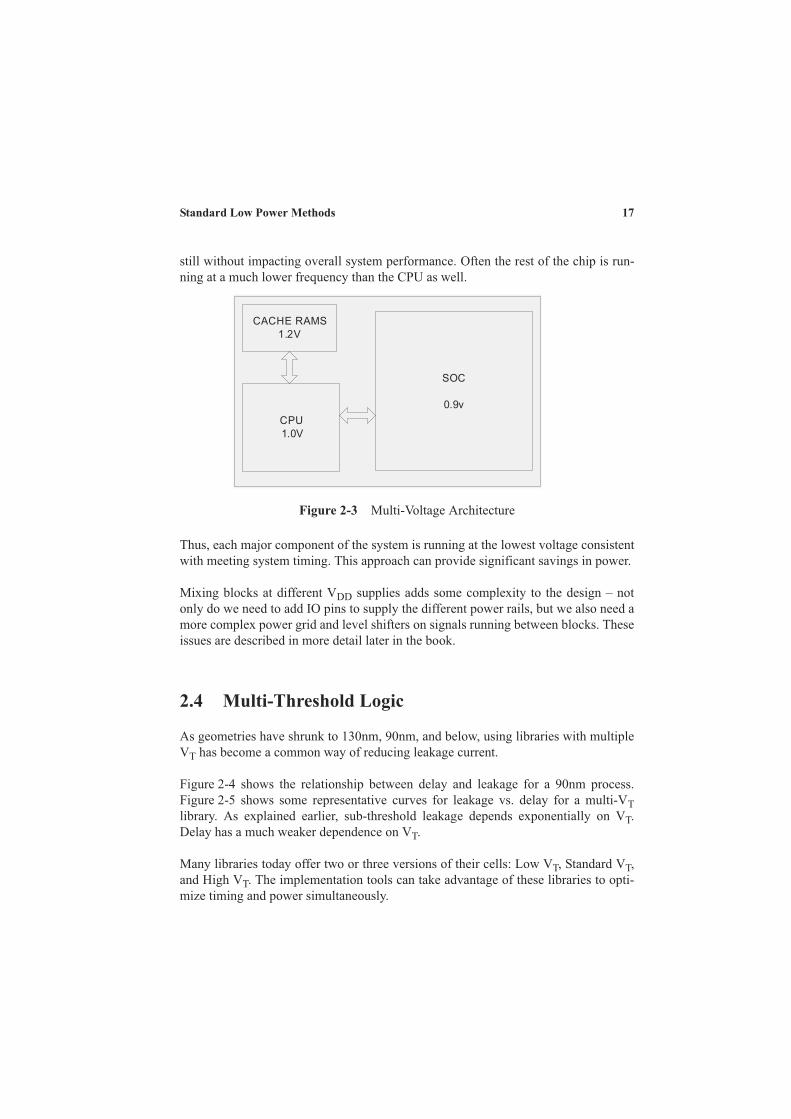
Standard Low Power Methods 17
still without impacting overall system performance. Often the rest of the chip is run-
ning at a much lower frequency than the CPU as well.
Figure 2-3 Multi-Voltage Architecture
Thus, each major component of the system is running at the lowest voltage consistent
with meeting system timing. This approach can provide significant savings in power.
Mixing blocks at different VDD supplies adds some complexity to the design – not
only do we need to add IO pins to supply the different power rails, but we also need a
more complex power grid and level shifters on signals running between blocks. These
issues are described in more detail later in the book.
2.4 Multi-Threshold Logic
As geometries have shrunk to 130nm, 90nm, and below, using libraries with multiple
VT has become a common way of reducing leakage current.
Figure 2-4 shows the relationship between delay and leakage for a 90nm process.
Figure 2-5 shows some representative curves for leakage vs. delay for a multi-VT
library. As explained earlier, sub-threshold leakage depends exponentially on VT.
Delay has a much weaker dependence on VT.
Many libraries today offer two or three versions of their cells: Low VT, Standard VT,
and High VT. The implementation tools can take advantage of these libraries to opti-
mize timing and power simultaneously.
SOC
0.9v
CPU
1.0V
CACHE RAMS
1.2V