low power design verification of complex chips
TRANSCRIPT

1
Narasimha KarunakarAMD India Ltd
Challenges, Possible Solutions and Flow Changes for Low Power Design Verification of
Complex Chips

2
AgendaLow power design techniques overviewPower Aware Verification (PAV) challengesPossible solutionsDesign guidelinesVerification guidelines

3
Low Power Design Techniques: Requirement than Improvement
Higher clock frequencies + Higher device density => High power dissipationConflicts with increasing importance on battery life and power savingsExponential growth in usage of Handhelds/Laptops/MobilesPerformance/Watt is the new mantra!!
4
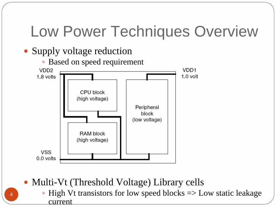
Low Power Techniques OverviewSupply voltage reduction
Based on speed requirement
Multi-Vt (Threshold Voltage) Library cellsHigh Vt transistors for low speed blocks => Low static leakage current
5
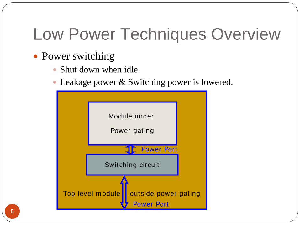
Low Power Techniques OverviewPower switching
Shut down when idle.Leakage power & Switching power is lowered.
Top level module outside power gating
Module under
Power gating
Switching circuit
Power Port
Power Port

6
Low Power Techniques Overview
Level shifter
Isolation cell
7
Next…Low power design techniques overviewPower Aware Verification (PAV) challengesPossible solutionsDesign guidelinesVerification guidelines

8
Power Aware Verification challengesConventional verification infrastructure is not PAV ready
No notion of voltage/powerProtection gates modeling absent in RTLPower Ports & Power Switches not modeledChecks on missing protection gates not done

9
Power Aware Verification challengesPower up and Recovery sequence checks inadequate
All voltage/power planes tied to 1’b1 or 1’b0 – no sequencingReset asserted at time 0 allows signals to be initialized at the beginning itselfFlops retain value even when domain is powered off

10
Next…Low power design techniques overviewPower Aware Verification (PAV) challengesPossible solutionsDesign guidelinesVerification guidelines
11
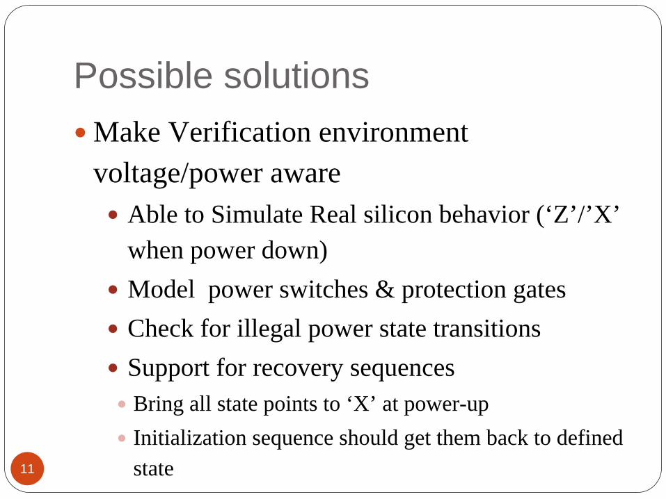
Possible solutionsMake Verification environment voltage/power aware
Able to Simulate Real silicon behavior (‘Z’/’X’when power down)Model power switches & protection gatesCheck for illegal power state transitionsSupport for recovery sequencesBring all state points to ‘X’ at power-up Initialization sequence should get them back to defined state

12
Possible solutions Some Tool vendors that address the above challenges
Synopsyso MVtools (MVSim & MVRC)o UPF (Unified Power Format)
Cadenceo Incisive verification flowo CPF (Common Power format)

13
Next…Low power design techniques overviewPower Aware Verification (PAV) challengesPossible solutionsDesign guidelinesVerification guidelines
14
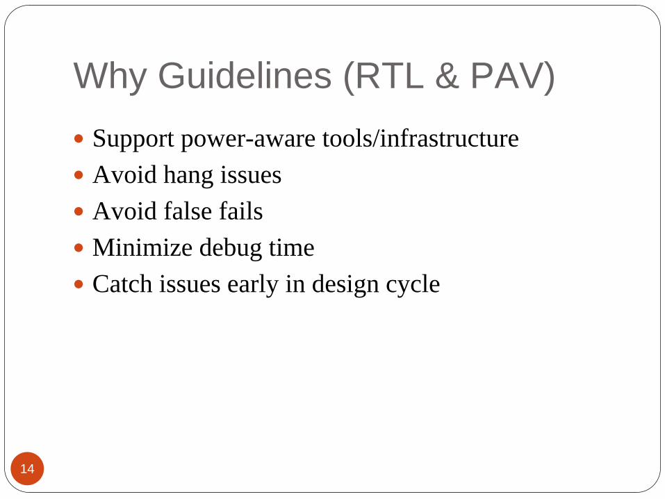
Why Guidelines (RTL & PAV)Support power-aware tools/infrastructureAvoid hang issuesAvoid false failsMinimize debug timeCatch issues early in design cycle
15
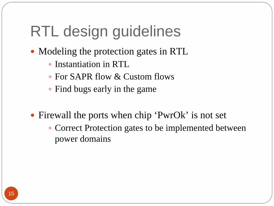
RTL design guidelinesModeling the protection gates in RTL
Instantiation in RTLFor SAPR flow & Custom flowsFind bugs early in the game
Firewall the ports when chip ‘PwrOk’ is not setCorrect Protection gates to be implemented between power domains

16
RTL design guidelinesPartition & Boundary
Voltage island boundaries alignmentNo Multiple Power domain in a final leaf moduleBelow Ex: a11 shouldn‘t have multiple power domains inside it.
TOP
A1
A2
A3a11
VDD_A1VDD_A1
VDD_A11 VDD_A3VDD_A3
VDD_A2
VSS
17
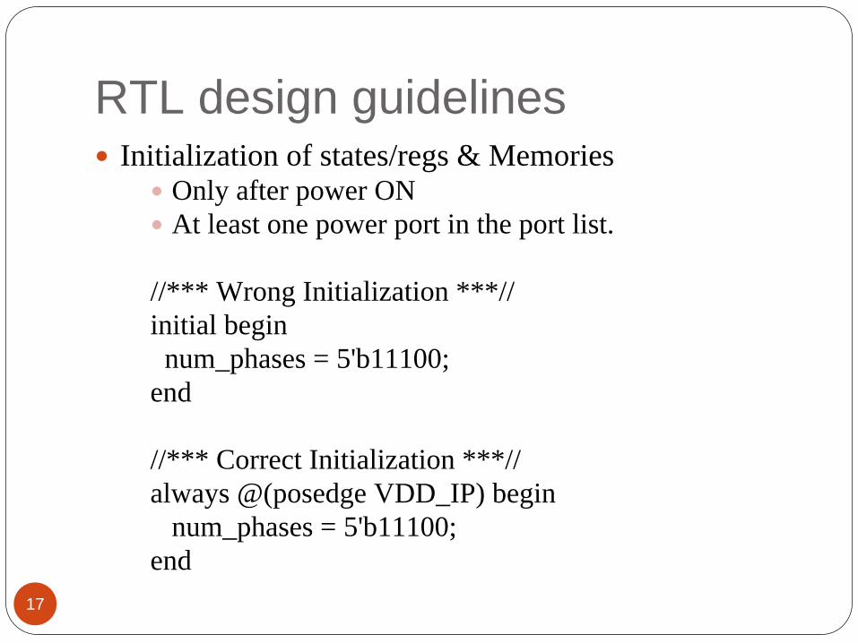
RTL design guidelinesInitialization of states/regs & Memories
Only after power ONAt least one power port in the port list.
//*** Wrong Initialization ***//initial beginnum_phases = 5'b11100;
end
//*** Correct Initialization ***//always @(posedge VDD_IP) begin
num_phases = 5'b11100; end

18
RTL design guidelinesExpression in instantiation
Wrong/No power domain assigned to ‘AND’
IP1 instance_a (.A_B ( A & B),....
);
IP1 on PD1 A_B ANDANDANDANDANDANDANDANDANDAND A
B IP2 on PD2

19
RTL design guidelinesAvoid Constants in Port mapping
Avoid constants (1'b1/1'b0) & shouldn’t cross domain boundaries
module modA;modB inst_modB (.in1(abc), .in2(1'b0));//DOMAIN_B
endmodule
module top; modA inst_modA (.vdd_main(vdd_main),
.vdd_sub(vdd_sub));endmodule
top
vdd_main
vdd_sub
modA
in1
modB in2
Power Ports
20
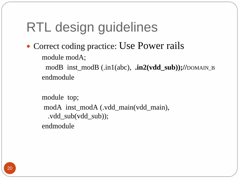
RTL design guidelinesCorrect coding practice: Use Power rails
module modA;modB inst_modB (.in1(abc), .in2(vdd_sub));//DOMAIN_B
endmodule
module top; modA inst_modA (.vdd_main(vdd_main),
.vdd_sub(vdd_sub));endmodule
21
Next…Low power design techniques overviewPower Aware Verification (PAV) challengesPossible solutionsDesign guidelinesVerification guidelines
22
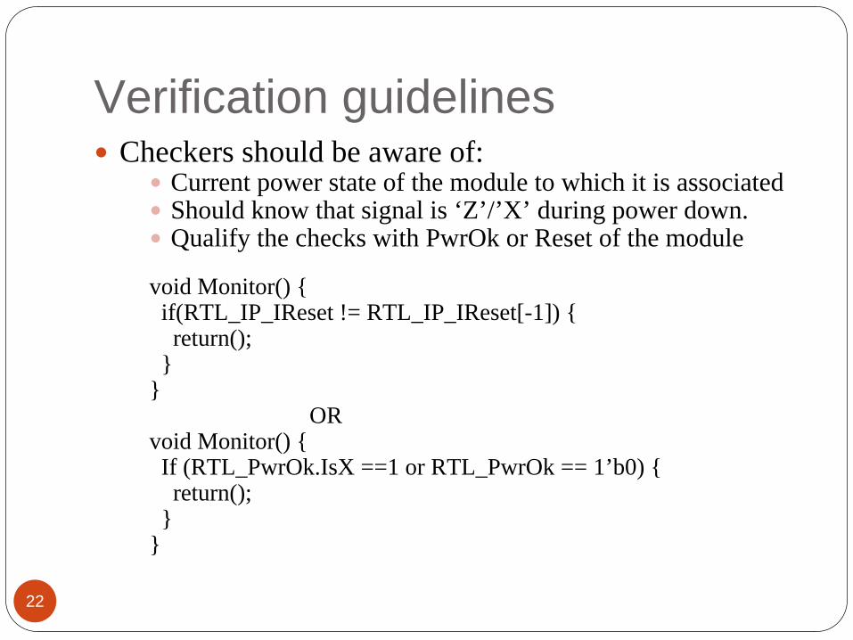
Verification guidelinesCheckers should be aware of:
Current power state of the module to which it is associatedShould know that signal is ‘Z’/’X’ during power down.Qualify the checks with PwrOk or Reset of the module
void Monitor() {if(RTL_IP_IReset != RTL_IP_IReset[-1]) {return();
}}
ORvoid Monitor() {If (RTL_PwrOk.IsX ==1 or RTL_PwrOk == 1’b0) {return();
}}

23
Verification guidelinesAlways assume 4-state values for RTL signals:
Qualify the control signal to see if it is ‘Z’/’X’Then check for correct value of the signal (1’b1 or 1’b0)In C/C++ Domain ‘X’ is seen as 1’b1 & ‘Z’ is seen as 1’b0

24
Verification guidelines// *** Wrong coding ***//void Monitor() {
if(RTL_BIST_Complete == 1) {…
// checks//}
// *** Correct coding ***//void Monitor() {if (RTL_BIST_Complete == 1 && RTL_BIST_Complete.IsXorZ()
!= 1) {…
// checks//}

25
Verification guidelines• Test plan is to check if it is not ‘X’ or ‘Z’
// *** Correct coding ***//void Monitor() {if (IntState == SLEEP) {
if(RTL_DramReset.IsXorZ() == 1 || RTL_DramReset == 1) {Error (“Un-expected X/Z”);
} else {}

26
ReferencesDiagrams on “Power reduction techniques”
Synopsys Low-Power Flow User Guide (Version A-2007.12, December 2007)

27
Good Bye
THANKS FOR YOUR TIME