low-power chemical sensing applications...
TRANSCRIPT

LMP91000January 18, 2011
Sensor AFE System: Configurable AFE Potentiostat forLow-Power Chemical Sensing ApplicationsGeneral DescriptionThe LMP91000 is a programmable Analog Front End (AFE)for use in micro-power electrochemical sensing applications.It provides a complete signal path solution between a sensorand a microcontroller that generates an output voltage pro-portional to the cell current. The LMP91000’s programmabilityenables it to support multiple electrochemical sensors suchas 3-lead toxic gas sensors and 2-lead galvanic cell sensorswith a single design as opposed to the multiple discrete so-lutions. The LMP91000 supports gas sensitivities over arange of 0.5 nA/ppm to 9500 nA/ppm. It also allows for aneasy conversion of current ranges from 5µA to 750µA fullscale.
The LMP91000’s adjustable cell bias and transimpedanceamplifier (TIA) gain are programmable through the the I2C in-terface. The I2C interface can also be used for sensor diag-nostics. An integrated temperature sensor can be read by theuser through the VOUT pin and used to provide additionalsignal correction in the µC or monitored to verify temperatureconditions at the sensor.
The LMP91000 is optimized for micro-power applications andoperates over a voltage range of 2.7V to 5.25V. The total cur-rent consumption can be less than 10μA. Further power sav-ings are possible by switching off the TIA amplifier andshorting the reference electrode to the working electrode withan internal switch.
FeaturesTypical Values, TA = 25°C
Supply voltage 2.7 V to 5.25 V
Supply current (average over time) <10 µA
Cell conditioning current up to 10 mA
Reference electrode bias current (85°C) 900pA (max)
Output drive current 750µA
Complete potentiostat circuit to interface to most chemicalcells
Programmable cell bias voltage
Low bias voltage drift
Programmable TIA gain 2.75kΩ to 350kΩ Sink and source capability
I2C compatible digital interface
Ambient operating temperature -40°C to 85°C
Package 14 pin LLP
Supported by Webench Sensor AFE Designer
Applications Chemical species identification
Amperometric applications
Electrochemical blood glucose meter
Typical Application
30132505
AFE Gas Detector
© 2011 National Semiconductor Corporation 301325 www.national.com
LM
P91000 S
en
so
r AF
E S
yste
m: C
on
figu
rab
le A
FE
Po
ten
tiosta
t for L
ow
-Po
wer C
hem
ical S
en
sin
gA
pp
licatio
ns

Ordering Information
Package Part NumberPackage
MarkingTransport Media NSC Drawing
14-Pin LLP
LMP91000SD
L91000
1k Units Tape and Reel
SDA14BLMP91000SDE 250 Units Tape and Reel
LMP91000SDX 4.5k Units Tape and Reel
Connection Diagram
14–Pin LLP
30132502
Top View
Pin Descriptions
Pin Name Description
1 DGND Connect to ground
2 MENB Module Enable, Active Low
3 SCL Clock signal for I2C compatible interface
4 SDA Data for I2C compatible interface
5 NC Not Internally Connected
6 VDD Supply Voltage
7 AGND Ground
8 VOUT Analog Output
9 C2 External filter connector (Filter between C1 and C2)
10 C1 External filter connector (Filter between C1 and C2)
11 VREF Voltage Reference input
12 WE Working Electrode. Output to drive the Working Electrode of the chemical
sensor
13 RE Reference Electrode. Input to drive Counter Electrode of the chemical sensor
14 CE Counter Electrode. Output to drive Counter Electrode of the chemical sensor
DAP Connect to AGND
www.national.com 2
LM
P91000

Absolute Maximum Ratings (Note 1)
If Military/Aerospace specified devices are required,please contact the National Semiconductor Sales Office/Distributors for availability and specifications.
ESD Tolerance (Note 2)
Human Body Model 2kV
Charge-Device Model 1kV
Machine Model 200V
Voltage between any two pins 6.0V
Current through VDD or VSS 50mA
Current sunk and sourced by CE pin 10mA
Current out of other pins(Note 3) 5mA
Storage Temperature Range -65°C to 150°C
Junction Temperature (Note 4) 150°C
For soldering specifications:
see product folder at www.national.com and
www.national.com/ms/MS/MS-SOLDERING.pdf
Operating Ratings (Note 1)
Supply Voltage VS=(VDD - AGND) 2.7V to 5.25V
Temperature Range (Note 4) -40°C to 85°C
Package Thermal Resistance (Note 4)
14-Pin LLP (θJA) 44 °C/W
Electrical Characteristics (Note 5)
Unless otherwise specified, all limits guaranteed for TA = 25°C, VS=(VDD – AGND), VS=3.3V and AGND = DGND =0V,VREF= 2.5V, Internal Zero= 20% VREF. Boldface limits apply at the temperature extremes.
Symbol Parameter ConditionsMin
(Note 7)
Typ
(Note 6)
Max
(Note 7)Units
Power Supply Specification
IS Supply Current 3-lead amperometric cell mode
MODECN = 0x03 10
15
13.5
µA
Standby mode
MODECN = 0x02 6.5
10
8
Temperature Measurement mode with TIA OFF
MODECN = 0x06 11.4
15
13.5
Temperature Measurement mode with TIA ON
MODECN = 0x07 14.9
20
18
2-lead ground referred galvanic cell mode
VREF=1.5V
MODECN = 0x01
6.29
8
Deep Sleep mode
MODECN = 0x00 0.6
1
0.85
Potentiostat
Bias_RW Bias Programming range
(differential voltage between RE
pin and WE pin)
Percentage of voltage referred to VREF or VDD
±24 %
Bias Programming Resolution First two smallest step ±1 %
All other steps ±2
IRE Input bias current at RE pin
VDD=2.7V;
Internal Zero 50% VDD
-90
-800
90
800pA
VDD=5.25V;
Internal Zero 50% VDD
-90
-900
90
900
ICE Minimum operating current
capability
sink 750 µA
source 750
Minimum charging capability
(Note 9)
sink 10 mA
source 10
AOL_A1 Open loop voltage gain of
control loop op amp (A1)300mV≤VCE≤Vs-300mV;
-750µA≤ICE≤750µA104 120 dB
en_RW Low Frequency integrated noise
between RE pin and WE pin
0.1Hz to 10Hz, Zero Bias
(Note 10) 3.4
µVpp0.1Hz to 10Hz, with Bias
(Note 10, Note 11) 5.1
3 www.national.com
LM
P91000
Symbol Parameter ConditionsMin
(Note 7)
Typ
(Note 6)
Max
(Note 7)Units
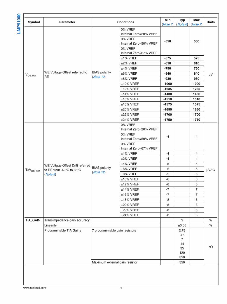
VOS_RW
WE Voltage Offset referred to
RE
BIAS polarity
(Note 12)
0% VREF
Internal Zero=20% VREF
-550 550
µV
0% VREF
Internal Zero=50% VREF
0% VREF
Internal Zero=67% VREF
±1% VREF -575 575
±2% VREF -610 610
±4% VREF -750 750
±6% VREF -840 840
±8% VREF -930 930
±10% VREF -1090 1090
±12% VREF -1235 1235
±14% VREF -1430 1430
±16% VREF -1510 1510
±18% VREF -1575 1575
±20% VREF -1650 1650
±22% VREF -1700 1700
±24% VREF -1750 1750
TcVOS_RW
WE Voltage Offset Drift referred
to RE from -40°C to 85°C
(Note 8)
BIAS polarity
(Note 12)
0% VREF
Internal Zero=20% VREF
-4 4
µV/°C
0% VREF
Internal Zero=50% VREF
0% VREF
Internal Zero=67% VREF
±1% VREF -4 4
±2% VREF -4 4
±4% VREF -5 5
±6% VREF -5 5
±8% VREF -5 5
±10% VREF -6 6
±12% VREF -6 6
±14% VREF -7 7
±16% VREF -7 7
±18% VREF -8 8
±20% VREF -8 8
±22% VREF -8 8
±24% VREF -8 8
TIA_GAIN Transimpedance gain accuracy 5 %
Linearity ±0.05 %
Programmable TIA Gains 7 programmable gain resistors
2.75
3.5
7
14
35
120
350
kΩ
Maximum external gain resistor 350
www.national.com 4
LM
P91000
Symbol Parameter ConditionsMin
(Note 7)
Typ
(Note 6)
Max
(Note 7)Units
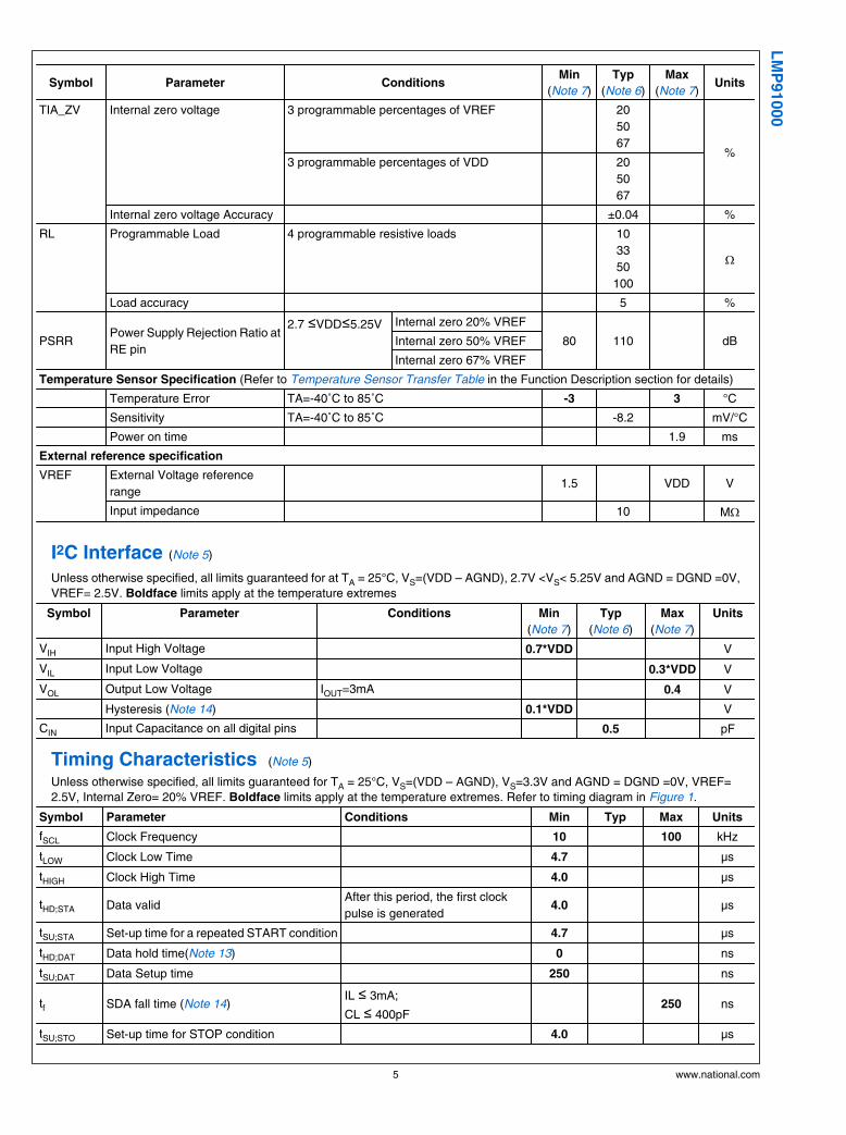
TIA_ZV Internal zero voltage 3 programmable percentages of VREF
20
50
67
%3 programmable percentages of VDD
20
50
67
Internal zero voltage Accuracy ±0.04 %
RL Programmable Load 4 programmable resistive loads
10
33
50
100
Ω
Load accuracy 5 %
PSRRPower Supply Rejection Ratio at
RE pin
2.7 ≤VDD≤5.25V Internal zero 20% VREF
80 110 dBInternal zero 50% VREF
Internal zero 67% VREF
Temperature Sensor Specification (Refer to Temperature Sensor Transfer Table in the Function Description section for details)
Temperature Error TA=-40˚C to 85˚C -3 3 °C
Sensitivity TA=-40˚C to 85˚C -8.2 mV/°C
Power on time 1.9 ms
External reference specification
VREF External Voltage reference
range
1.5 VDD V
Input impedance 10 MΩ
I2C Interface (Note 5)
Unless otherwise specified, all limits guaranteed for at TA = 25°C, VS=(VDD – AGND), 2.7V <VS< 5.25V and AGND = DGND =0V,VREF= 2.5V. Boldface limits apply at the temperature extremes
Symbol Parameter Conditions Min
(Note 7)
Typ
(Note 6)
Max
(Note 7)
Units
VIH Input High Voltage 0.7*VDD V
VIL Input Low Voltage 0.3*VDD V
VOL Output Low Voltage IOUT=3mA 0.4 V
Hysteresis (Note 14) 0.1*VDD V
CIN Input Capacitance on all digital pins 0.5 pF
Timing Characteristics (Note 5)
Unless otherwise specified, all limits guaranteed for TA = 25°C, VS=(VDD – AGND), VS=3.3V and AGND = DGND =0V, VREF=2.5V, Internal Zero= 20% VREF. Boldface limits apply at the temperature extremes. Refer to timing diagram in Figure 1.
Symbol Parameter Conditions Min Typ Max Units
fSCL Clock Frequency 10 100 kHz
tLOW Clock Low Time 4.7 µs
tHIGH Clock High Time 4.0 µs
tHD;STA Data validAfter this period, the first clock
pulse is generated4.0 µs
tSU;STA Set-up time for a repeated START condition 4.7 µs
tHD;DAT Data hold time(Note 13) 0 ns
tSU;DAT Data Setup time 250 ns
tf SDA fall time (Note 14)IL ≤ 3mA;
CL ≤ 400pF 250 ns
tSU;STO Set-up time for STOP condition 4.0 µs
5 www.national.com
LM
P91000

Symbol Parameter Conditions Min Typ Max Units
tBUF
Bus free time between a STOP and START
condition
4.7 µs
tVD;DAT Data valid time 3.45 µs
tVD;ACK Data valid acknowledge time 3.45 µs
tSP Pulse width of spikes that must be
suppressed by the input filter(Note 14)
50 ns
t_timeout SCL and SDA Timeout 25 100 ms
tEN;START I2C Interface Enabling 600 ns
tEN;STOP I2C Interface Disabling 600 ns
tEN;HIGH time between consecutive I2C interface
enabling and disabling
600 ns
Note 1: “Absolute Maximum Ratings” indicate limits beyond which damage to the device may occur, including inoperability and degradation of device reliabilityand/or performance. Functional operation of the device and/or non-degradation at the Absolute Maximum Ratings or other conditions beyond those indicated inthe Operating Ratings is not implied. Operating Ratings indicate conditions at which the device is functional and the device should not be operated beyond suchconditions.
Note 2: Human Body Model, applicable std. MIL-STD-883, Method 3015.7. Machine Model, applicable std. JESD22-A115-A (ESD MM std. of JEDEC) Field-Induced Charge-Device Model, applicable std. JESD22-C101-C (ESD FICDM std. of JEDEC).
Note 3: All non-power pins of this device are protected against ESD by snapback devices. Voltage at such pins will rise beyond absmax if current is forced intopin.
Note 4: The maximum power dissipation is a function of TJ(MAX), θJA, and the ambient temperature, TA. The maximum allowable power dissipation at any ambienttemperature is PDMAX = (TJ(MAX) - TA)/ θJA All numbers apply for packages soldered directly onto a PC board.
Note 5: Electrical Table values apply only for factory testing conditions at the temperature indicated. Factory testing conditions result in very limited self-heatingof the device such that TJ = TA. No guarantee of parametric performance is indicated in the electrical tables under conditions of internal self-heating where TJ >TA. Absolute Maximum Ratings indicate junction temperature limits beyond which the device may be permanently degraded, either mechanically or electrically.
Note 6: Typical values represent the most likely parametric norm as determined at the time of characterization. Actual typical values may vary over time and willalso depend on the application and configuration. The typical values are not tested and are not guaranteed on shipped production material.
Note 7: Limits are 100% production tested at 25°C. Limits over the operating temperature range are guaranteed through correlations using statistical qualitycontrol (SQC) method.
Note 8: Offset voltage temperature drift is determined by dividing the change in VOS at the temperature extremes by the total temperature change.
Starting from the measured voltage offset at temperature T1 (VOS_RW(T1)), the voltage offset at temperature T2 (VOS_RW(T2)) is calculated according the followingformula: VOS_RW(T2)=VOS_RW(T1)+ABS(T2–T1)* TcVOS_RW.
Note 9: At such currents no accuracy of the output voltage can be expected.
Note 10: This parameter includes both A1 and TIA's noise contribution.
Note 11: In case of external reference connected, the noise of the reference has to be added.
Note 12: For negative bias polarity the Internal Zero is set at 67% VREF.
Note 13: LMP91000 provides an internal 300ns minimum hold time to bridge the undefined region of the falling edge of SCL.
Note 14: This parameter is guaranteed by design or characterization.
Timing Diagram
30132541
FIGURE 1. I2C Interface Timing Diagram
www.national.com 6
LM
P91000

Typical Performance Characteristics Unless otherwise specified, TA = 25°C, VS=(VDD – AGND),
2.7V <VS< 5.25V and AGND = DGND =0V, VREF= 2.5V.
Input VOS_RW vs. temperature (Vbias 0mV)
-50 -25 0 25 50 75 100-300-280-260-240-220-200-180-160-140-120-100
VOS
(μV)
TEMPERATURE (°C)
VDD = 2.7VVDD = 3.3VVDD = 5V
30132563
Input VOS_RW vs. VDD (Vbias 0mV)
2.5 3.0 3.5 4.0 4.5 5.0 5.5-300-280-260-240-220-200-180-160-140-120-100
VOS
(μV)
SUPPLY VOLTAGE (V)
85°C25°C-40°C
30132562
IWE Step current response (rise)
NO
RM
ALIZ
ED O
UTP
UT
(200
mV/
DIV
)
TIME (200μs/DIV)
I WE
(50μ
A/D
IV)
IWE
2.75kΩ3.5kΩ7kΩ14kΩ35kΩ120kΩ350kΩ
30132564
IWE Step current response (fall)
NO
RM
ALIZ
ED O
UTP
UT
TIA
(200
mV/
DIV
)
TIME (200μs/DIV)
I WE
(50μ
A/D
IV)
IWE
2.75kΩ3.5kΩ7kΩ14kΩ35kΩ120kΩ350kΩ
30132566
AC PSRR vs. Frequency
10 100 1k 10k 100k80
90
100
110
120
130
140
PSR
R (d
B)
FREQUENCY (Hz)
30132560
Temperature sensor output vs. VDD (Temperature = 30°C)
2.5 3.0 3.5 4.0 4.5 5.0 5.51310
1312
1314
1316
1318
1320
VOU
T (m
V)
SUPPLY VOLTAGE (V)
30132569
7 www.national.com
LM
P91000

Supply current vs. temperature (Deep Sleep Mode)
-50 -25 0 25 50 75 1000.1
0.2
0.3
0.4
0.5
0.6
0.7
0.8
0.9
1.0
SUPP
LY C
UR
REN
T (μ
A)
TEMPERATURE (°C)
VDD = 2.7VVDD = 3.3VVDD = 5V
30132591
Supply current vs. VDD (Deep Sleep Mode)
2.5 3.0 3.5 4.0 4.5 5.0 5.50.1
0.2
0.3
0.4
0.5
0.6
0.7
0.8
0.9
1.0
SUPP
LY C
UR
REN
T (μ
A)
SUPPLY VOLTAGE (V)
85°C25°C-40°C
30132597
Supply current vs. temperature (Standby Mode)
-50 -25 0 25 50 75 1005.50
5.75
6.00
6.25
6.50
6.75
7.00
7.25
7.50
SUPP
LY C
UR
REN
T (μ
A)
TEMPERATURE (°C)
VDD = 2.7VVDD = 3.3VVDD = 5V
30132587
Supply current vs. VDD (Standby Mode)
2.5 3.0 3.5 4.0 4.5 5.0 5.55.50
5.75
6.00
6.25
6.50
6.75
7.00
7.25
7.50
SUPP
LY C
UR
REN
T (μ
A)
SUPPLY VOLTAGE (V)
85°C25°C-40°C
30132592
Supply current vs. temperature (3-lead amperometric Mode)
-50 -25 0 25 50 75 1009.09.29.49.69.8
10.010.210.410.610.811.0
SUPP
LY C
UR
REN
T (μ
A)
TEMPERATURE (°C)
VDD = 2.7VVDD = 3.3VVDD = 5V
30132586
Supply current vs. VDD (3-lead amperometric Mode)
2.5 3.0 3.5 4.0 4.5 5.0 5.59.09.29.49.69.8
10.010.210.410.610.811.0
SUPP
LY C
UR
REN
T (μ
A)
SUPPLY VOLTAGE (V)
85°C25°C-40°C
30132593
www.national.com 8
LM
P91000

Supply current vs. temperature (Temp Measurement TIA ON)
-50 -25 0 25 50 75 10013.0
13.5
14.0
14.5
15.0
15.5
16.0
16.5
17.0SU
PPLY
CU
RR
ENT
(μA)
TEMPERATURE (°C)
VDD = 2.7VVDD = 3.3VVDD = 5V
30132588
Supply current vs. VDD (Temp Measurement TIA ON)
2.5 3.0 3.5 4.0 4.5 5.0 5.514.014.214.414.614.815.015.215.415.615.816.0
SUPP
LY C
UR
REN
T (μ
A)
SUPPLY VOLTAGE (V)
85°C25°C-40°C
30132594
Supply current vs. temperature (Temp Measurement TIAOFF)
-50 -25 0 25 50 75 1009.0
9.5
10.0
10.5
11.0
11.5
12.0
12.5
13.0
SUPP
LY C
UR
REN
T (μ
A)
TEMPERATURE (°C)
VDD = 2.7VVDD = 3.3VVDD = 5V
30132589
Supply current vs. VDD (Temp Measurement TIA OFF)
2.5 3.0 3.5 4.0 4.5 5.0 5.510.0
10.5
11.0
11.5
12.0
12.5
13.0
SUPP
LY C
UR
REN
T (μ
A)
SUPPLY VOLTAGE (V)
85°C25°C-40°C
30132595
Supply current vs. temperature (2-lead ground referredamperometric Mode)
-50 -25 0 25 50 75 1005.005.255.505.756.006.256.506.757.007.257.50
SUPP
LY C
UR
REN
T (μ
A)
TEMPERATURE (°C)
VDD = 2.7VVDD = 3.3VVDD = 5V
30132590
Supply current vs. VDD (2-lead ground referredamperometric Mode)
2.5 3.0 3.5 4.0 4.5 5.0 5.55.0
5.5
6.0
6.5
7.0
7.5
8.0
8.5
9.0
SUPP
LY C
UR
REN
T (μ
A)
SUPPLY VOLTAGE (V)
85°C25°C-40°C
30132596
9 www.national.com
LM
P91000

0.1Hz to 10Hz noise, 0V bias
0 1 2 3 4 5 6 7 8 9 10-1.5
-1.0
-0.5
0.0
0.5
1.0
1.5
EN_R
W (μ
V)
TIME (s)
30132598
0.1Hz to 10Hz noise, 300mV bias
0 1 2 3 4 5 6 7 8 9 10-2.5-2.0-1.5-1.0-0.50.00.51.01.52.02.5
EN_R
W (μ
V)
TIME (s)
30132599
0.1Hz to 10Hz noise, 600mV bias
0 1 2 3 4 5 6 7 8 9 10-2.5-2.0-1.5-1.0-0.50.00.51.01.52.02.5
EN_R
W (μ
V)
TIME (s)
301325100
A VOUT step response 100 ppm to 400 ppm CO(CO gas sensor connected to LMP91000)
0 25 50 75 100 125 1501.0
1.1
1.2
1.3
1.4
1.5
1.6
1.7
1.8
1.9
2.0
VOU
T (V
)
TIME (s)
RTIA=35kΩ,Rload=10Ω,VREF=5V
LMP91000
30132568
www.national.com 10
LM
P91000

Function Description
GENERAL
The LMP91000 is a programmable AFE for use in micropowerchemical sensing applications. The LMP91000 is designedfor 3-lead single gas sensors and for 2-lead galvanic cell sen-sors. This device provides all of the functionality for detectingchanges in gas concentration based on a delta current at theworking electrode. The LMP91000 generates an output volt-age proportional to the cell current. Transimpedance gain isuser programmable through an I2C compatible interface from2.75kΩ to 350kΩ making it easy to convert current rangesfrom 5µA to 750µA full scale. Optimized for micro-power ap-plications, the LMP91000 AFE works over a voltage range of
2.7V to 5.25 V. The cell voltage is user selectable using theon board programmability. In addition, it is possible to connectan external transimpedance gain resistor. A temperature sen-sor is embedded and it can be power cycled through theinterface. The output of this temperature sensor can be readby the user through the VOUT pin. It is also possible to haveboth temperature output and output of the TIA at the sametime; the pin C2 is internally connected to the output of thetransimpedance (TIA), while the temperature is available atthe VOUT pin. Depending on the configuration, total currentconsumption for the device can be less than 10µA. For powersavings, the transimpedance amplifier can be turned off andinstead a load impedance equivalent to the TIA’s inputsimpedance is switched in.
30132583
FIGURE 2. System Block Diagram
POTENTIOSTAT CIRCUITRY
The core of the LMP91000 is a potentiostat circuit. It consistsof a differential input amplifier used to compare the potentialbetween the working and reference electrodes to a requiredworking bias potential (set by the Variable Bias circuitry).The error signal is amplified and applied to the counter elec-trode (through the Control Amplifier - A1). Any changes inthe impedance between the working and reference elec-trodes will cause a change in the voltage applied to thecounter electrode, in order to maintain the constant voltagebetween working and reference electrodes. A Tran-simpedance Amplifier connected to the working electrode,is used to provide an output voltage that is proportional to thecell current. The working electrode is held at virtual ground(Internal ground) by the transimpedance amplifier. The po-tentiostat will compare the reference voltage to the desiredbias potential and adjust the voltage at the counter electrodeto maintain the proper working-to-reference voltage.
Transimpedance amplifier
The transimpedance amplifier (TIA in Figure 2) has 7 pro-grammable internal gain resistors. This accommodates thefull scale ranges of most existing sensors. Moreover an ex-ternal gain resistor can be connected to the LMP91000 be-tween C1 and C2 pins. The gain is set through the I2Cinterface.
Control amplifier
The control amplifier (A1 op amp in Figure 2) has two tasks:a) providing initial charge to the sensor, b) providing a biasvoltage to the sensor. A1 has the capability to drive up to 10-mA into the sensor in order to to provide a fast initial condi-tioning. A1 is able to sink and source current according to theconnected gas sensor (reducing or oxidizing gas sensor). Itcan be powered down to reduce system power consumption.However powering down A1 is not recommended, as it maytake a long time for the sensor to recover from this situation.
Variable Bias
The Variable Bias block circuitry (Figure 2) provides theamount of bias voltage required by a biased gas sensor be-tween its reference and working electrodes. The bias voltagecan be programmed to be 1% to 24% (14 steps in total) of thesupply, or of the external reference voltage. The 14 steps canbe programmed through the I2C interface. The polarity of thebias can be also programmed.
Internal zero
The internal Zero is the voltage at the non-inverting pin of theTIA. The internal zero can be programmed to be either 67%,50% or 20%, of the supply, or the external reference voltage.This provides both sufficient headroom for the counter elec-trode of the sensor to swing, in case of sudden changes in thegas concentration, and best use of the ADC’s full scale inputrange.
11 www.national.com
LM
P91000

The Internal zero is provided through an internal voltage di-vider (Vref divider box in Figure 2). The divider is programmedthrough the I2C interface.
Temperature sensor
The embedded temperature sensor can be switched off dur-ing gas concentration measurement to save power. The tem-perature measurement is triggered through the I2C interface.The temperature output is available at the VOUT pin until theconfiguration bit is reset. The output signal of the temperaturesensor is a voltage, referred to the ground of the LMP91000(AGND).
Temperature Sensor Transfer Table
Temperature
(°C)
Output
Voltage
(mV)
Temperature
(°C)
Output
Voltage
(mV)
-40 1875 23 1375
-39 1867 24 1367
-38 1860 25 1359
-37 1852 26 1351
-36 1844 27 1342
-35 1836 28 1334
-34 1828 29 1326
-33 1821 30 1318
-32 1813 31 1310
-31 1805 32 1302
-30 1797 33 1293
-29 1789 34 1285
-28 1782 35 1277
-27 1774 36 1269
-26 1766 37 1261
-25 1758 38 1253
-24 1750 39 1244
-23 1742 40 1236
-22 1734 41 1228
-21 1727 42 1220
-20 1719 43 1212
-19 1711 44 1203
-18 1703 45 1195
-17 1695 46 1187
-16 1687 47 1179
-15 1679 48 1170
-14 1671 49 1162
-13 1663 50 1154
-12 1656 51 1146
-11 1648 52 1137
-10 1640 53 1129
-9 1632 54 1121
-8 1624 55 1112
-7 1616 56 1104
-6 1608 57 1096
-5 1600 58 1087
-4 1592 59 1079
-3 1584 60 1071
-2 1576 61 1063
-1 1568 62 1054
0 1560 63 1046
1 1552 64 1038
2 1544 65 1029
3 1536 66 1021
4 1528 67 1012
5 1520 68 1004
6 1512 69 996
7 1504 70 987
8 1496 71 979
9 1488 72 971
10 1480 73 962
11 1472 74 954
12 1464 75 945
13 1456 76 937
14 1448 77 929
15 1440 78 920
16 1432 79 912
17 1424 80 903
18 1415 81 895
19 1407 82 886
20 1399 83 878
21 1391 84 870
22 1383 85 861
Although the temperature sensor is very linear, its responsedoes have a slight downward parabolic shape. This shape isvery accurately reflected in the temperature sensor TransferTable. For a linear approximation, a line can easily be calcu-lated over the desired temperature range from the Table usingthe two-point equation:
V-V1=((V2–V1)/(T2–T1))*(T-T1)
Where V is in mV, T is in °C, T1 and V1 are the coordinates ofthe lowest temperature, T2 and V2 are the coordinates of thehighest temperature.
For example, if we want to determine the equation of a lineover a temperature range of 20°C to 50°C, we would proceedas follows:
V-1399mV=((1154mV - 1399mV)/(50°C -20°C))*(T-20°C)
V-1399mV= -8.16mV/°C*(T-20°C)
V=(-8.16mV/°C)*T+1562.2mV
Using this method of linear approximation, the transfer func-tion can be approximated for one or more temperature rangesof interest.
I2C INTERFACE
The I2C compatible interface operates in Standard mode(100kHz). Pull-up resistors or current sources are required onthe SCL and SDA pins to pull them high when they are notbeing driven low. A logic zero is transmitted by driving theoutput low. A logic high is transmitted by releasing the outputand allowing it to be pulled-up externally. The appropriatepull-up resistor values will depend upon the total bus capac-itance and operating speed. The LMP91000 comes with a 7bit bus fixed address: 1001 000.
www.national.com 12
LM
P91000
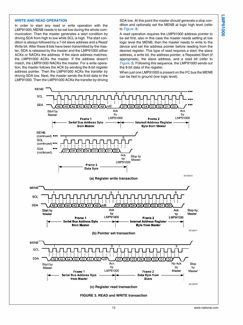
WRITE AND READ OPERATION
In order to start any read or write operation with theLMP91000, MENB needs to be set low during the whole com-munication. Then the master generates a start condition bydriving SDA from high to low while SCL is high. The start con-dition is always followed by a 7-bit slave address and a Read/Write bit. After these 8 bits have been transmitted by the mas-ter, SDA is released by the master and the LMP91000 eitherACKs or NACKs the address. If the slave address matches,the LMP91000 ACKs the master. If the address doesn'tmatch, the LMP91000 NACKs the master. For a write opera-tion, the master follows the ACK by sending the 8-bit registeraddress pointer. Then the LMP91000 ACKs the transfer bydriving SDA low. Next, the master sends the 8-bit data to theLMP91000. Then the LMP91000 ACKs the transfer by driving
SDA low. At this point the master should generate a stop con-dition and optionally set the MENB at logic high level (referto Figure 3).
A read operation requires the LMP91000 address pointer tobe set first, also in this case the master needs setting at lowlogic level the MENB, then the master needs to write to thedevice and set the address pointer before reading from thedesired register. This type of read requires a start, the slaveaddress, a write bit, the address pointer, a Repeated Start (ifappropriate), the slave address, and a read bit (refer toFigure 3). Following this sequence, the LMP91000 sends outthe 8-bit data of the register.
When just one LMP91000 is present on the I2C bus the MENBcan be tied to ground (low logic level).
30132572
(a) Register write transaction
30132571
(b) Pointer set transaction
30132570
(c) Register read transaction
FIGURE 3. READ and WRITE transaction
13 www.national.com
LM
P91000
TIMEOUT FEATURE
The timeout is a safety feature to avoid bus lockup situation.If SCL is stuck low for a time exceeding t_timeout, theLMP91000 will automatically reset its I2C interface. Also, inthe case the LMP91000 hangs the SDA for a time exceeding
t_timeout, the LMP91000’s I2C interface will be reset so thatthe SDA line will be released. Since the SDA is an open-drainwith an external resistor pull-up, this also avoids high powerconsumption when LMP91000 is driving the bus and the SCLis stopped.
REGISTERS
The registers are used to configure the LMP91000.
If writing to a reserved bit, user must write only 0. Readback value is unspecified and should be discarded.
Register map
Address Name Power on default Access Lockable?
0x00 STATUS 0x00 Read only N
0x01 LOCK 0x01 R/W N
0x02 through 0x09 RESERVED
0x10 TIACN 0x1C R/W Y
0x11 REFCN 0x00 R/W Y
0x12 MODECN 0x00 R/W N
0x13 through 0xFF RESERVED
STATUS -- Status Register (address 0x00)
The status bit is an indication of the LMP91000's power-on status. If its readback is “0”, the LMP91000 is not ready to accept otherI2C commands.
Bit Name Function
[7:1] RESERVED
0 STATUS
Status of Device
0 Not Ready (default)
1 Ready
LOCK -- Protection Register (address 0x01)
The lock bit enables and disables the writing of the TIACN and the REFCN registers. In order to change the content of the TIACNand the REFCN registers the lock bit needs to be set to “0”.
Bit Name Function
[7:1] RESERVED
0 LOCK
Write protection
0 Registers 0x10, 0x11 in write mode
1 Registers 0x10, 0x11 in read only mode (default)
www.national.com 14
LM
P91000

TIACN -- TIA Control Register (address 0x10)
The parameters in the TIA control register allow the configuration of the transimpedance gain (RTIA) and the load resistance(RLoad).
Bit Name Function
[7:5] RESERVED RESERVED
[4:2] TIA_GAIN
TIA feedback resistance selection
000 External resitance
001 2.75kΩ010 3.5kΩ011 7kΩ100 14kΩ101 35kΩ110 120kΩ111 350kΩ (default)
[1:0] RLOAD
RLoad selection
00 10Ω (default)
01 33Ω10 50Ω11 100Ω
REFCN -- Reference Control Register (address 0x11)
The parameters in the Reference control register allow the configuration of the Internal zero, Bias and Reference source. Whenthe Reference source is external, the reference is provided by a reference voltage connected to the VREF pin. In this condition theInternal Zero and the Bias voltage are defined as a percentage of VREF voltage instead of the supply voltage.
Bit Name Function
7 REF_SOURCE
Reference voltage source selection
0 Internal (default)
1 external
[6:5] INT_Z
Internal zero selection (Percentage of the source reference)
00 20% (default)
01 50%
10 67%
11 Internal zero circuitry bypassed (only in O2 ground referred measurement)
4 BIAS_SIGN
Selection of the Bias polarity
0 Positive (default)
1 Negative
[3:0] BIAS
BIAS selection (Percentage of the source reference)
0000 0% (default)
0001 1%
0010 2%
0011 4%
0100 6%
0101 8%
0110 10%
0111 12%
1000 14%
1001 16%
1010 18%
1011 20%
1100 22%
1101 24%
15 www.national.com
LM
P91000

MODECN -- Mode Control Register (address 0x12)
The Parameters in the Mode register allow the configuration of the Operation Mode of the LMP91000.
Bit Name Function
7 FET_SHORT
Shorting FET feature
0 Disabled (default)
1 Enabled
[6:3] RESERVED
[2:0] OP_MODE
Mode of Operation selection
000 Deep Sleep (default)
001 2-lead ground referred galvanic cell
010 Standby
011 3-lead amperometric cell
110 Temperature measurement (TIA OFF)
111 Temperature measurement (TIA ON)
When the LMP91000 is in Temperature measurement (TIA ON) mode, the output of the temperature sensor is present at the VOUTpin, while the output of the potentiostat circuit is available at pin C2.
GAS SENSOR INTERFACE
The LMP91000 supports both 3-lead and 2-lead gas sensors.Most of the toxic gas sensors are amperometric cells with 3leads (Counter, Worker and Reference). These leads shouldbe connected to the LMP91000 in the potentiostat topology.The 2-lead gas sensor (known as galvanic cell) should beconnected as simple buffer either referred to the ground of thesystem or referred to a reference voltage. The LMP91000support both connections for 2-lead gas sensor.
3-lead Amperometric Cell In Potentiostat Configuration
Most of the amperometric cell have 3 leads (Counter, Refer-ence and Working electrodes). The interface of the 3-lead gassensor to the LMP91000 is straightforward, the leads of thegas sensor need to be connected to the namesake pins of theLMP91000.
The LMP91000 is then configured in 3-lead amperometric cellmode; in this configuration the Control Amplifier (A1) is ONand provides the internal zero voltage and bias in case of bi-ased gas sensor. The transimpedance amplifier (TIA) is ON,it converts the current generated by the gas sensor in a volt-age, according to the transimpedance gain:
Gain=RTIA
If different gains are required, an external resistor can beconnected between the pins C1 and C2. In this case the in-ternal feedback resistor should be programmed to “external”.The RLoad together with the output capacitance of the gassensor acts as a low pass filter.
www.national.com 16
LM
P91000

30132583
FIGURE 4. 3-Lead Amperometric Cell
2-lead Galvanic Cell In Ground Referred Configuration
When the LMP91000 is interfaced to a galvanic cell (for in-stance to an Oxygen gas sensor) referred to the ground of thesystem, an external resistor needs to be placed in parallel tothe gas sensor; the negative electrode of the gas sensor isconnected to the ground of the system and the positive elec-trode to the Vref pin of the LMP91000, the working pin of theLMP91000 is connected to the ground.
The LMP91000 is then configured in 2-lead galvanic cellmode and the Vref bypass feature needs to be enabled. In
this configuration the Control Amplifier (A1) is turned off, andthe output of the gas sensor is amplified by the Tran-simpedance Amplifier (TIA) which is configured as a simplenon-inverting amplifier.
The gain of this non inverting amplifier is set according thefollowing formula
Gain= 1+(RTIA/RLoad)
If different gains are required, an external resistor can beconnected between the pins C1 and C2. In this case the in-ternal feedback resistor should be programmed to “external”.
17 www.national.com
LM
P91000
30132575
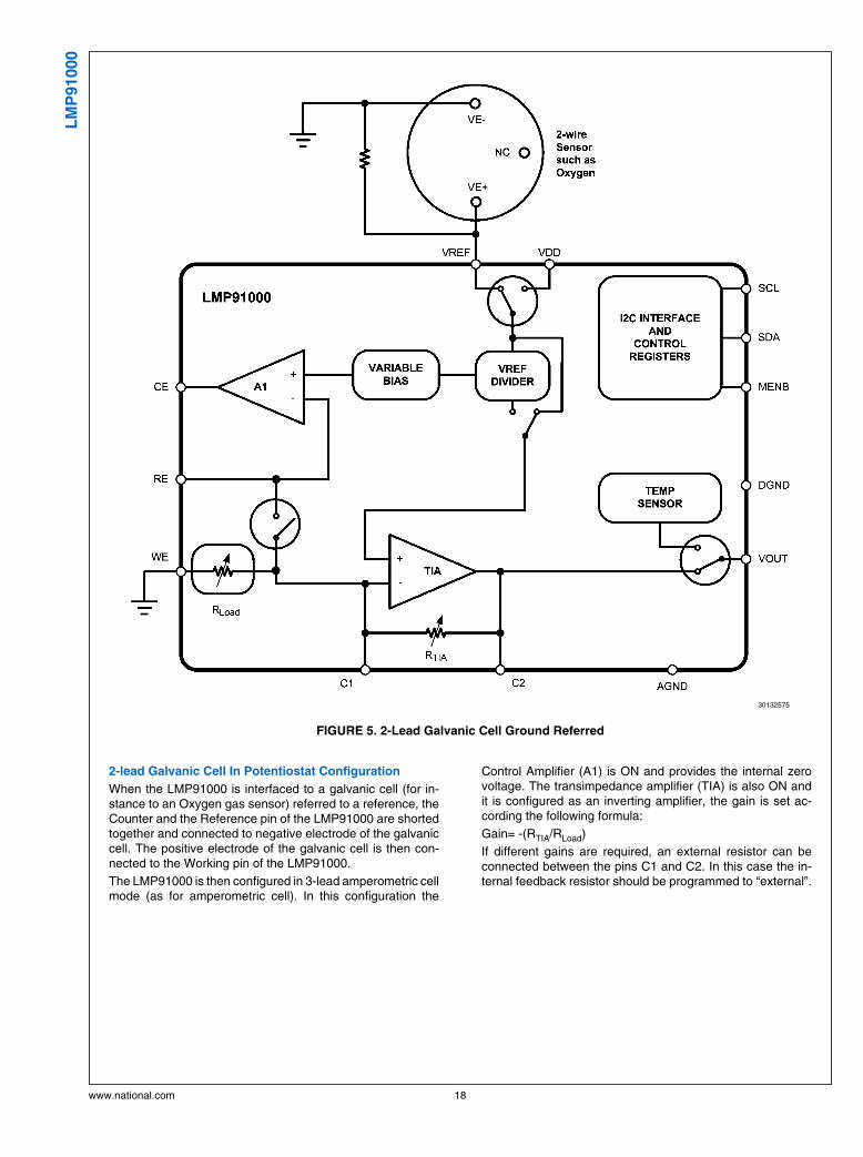
FIGURE 5. 2-Lead Galvanic Cell Ground Referred
2-lead Galvanic Cell In Potentiostat Configuration
When the LMP91000 is interfaced to a galvanic cell (for in-stance to an Oxygen gas sensor) referred to a reference, theCounter and the Reference pin of the LMP91000 are shortedtogether and connected to negative electrode of the galvaniccell. The positive electrode of the galvanic cell is then con-nected to the Working pin of the LMP91000.
The LMP91000 is then configured in 3-lead amperometric cellmode (as for amperometric cell). In this configuration the
Control Amplifier (A1) is ON and provides the internal zerovoltage. The transimpedance amplifier (TIA) is also ON andit is configured as an inverting amplifier, the gain is set ac-cording the following formula:
Gain= -(RTIA/RLoad)
If different gains are required, an external resistor can beconnected between the pins C1 and C2. In this case the in-ternal feedback resistor should be programmed to “external”.
www.national.com 18
LM
P91000

30132584
FIGURE 6. 2-Lead Galvanic Cell In Potentiostat Configuration
Application Information
CONNECTION OF MORE THAN ONE LMP91000 TO THEI2C BUS
The LMP91000 comes out with a unique and fixed I2C slaveaddress. It is still possible to connect more than oneLMP91000 to an I2C bus and select each device using theMENB pin. The MENB simply enables/disables the I2C com-munication of the LMP91000. When the MENB is at logic levellow all the I2C communication is enabled, it is disabled whenMENB is at high logic level.
In a system based on a μcontroller and more than oneLMP91000 connected to the I2C bus, the I2C lines (SDA and
SCL) are shared, while the MENB of each LMP91000 is con-nected to a dedicate GPIO port of the μcontroller.
The μcontroller starts communication asserting one out of NMENB signals where N is the total number of LMP91000sconnected to the I2C bus. Only the enabled device will ac-knowledge the I2C commands. After finishing communicatingwith this particular LMP91000, the microcontroller de-assertsthe corresponding MENB and repeats the procedure for otherLMP91000s. Figure 7 shows the typical connection whenmore than one LMP91000 is connected to the I2C bus.
30132581
FIGURE 7. More than one LMP91000 on I2C bus
19 www.national.com
LM
P91000

SMART GAS SENSOR ANALOG FRONT END
The LMP91000 together with an external EEPROM repre-sents the core of a SMART GAS SENSOR AFE. In theEEPROM it is possible to store the information related to theGAS sensor type, calibration and LMP91000's configuration(content of registers 10h, 11h, 12h). At startup the microcon-troller reads the EEPROM's content and configures theLMP91000. A typical smart gas sensor AFE is shown in Fig-ure 8. The connection of MENB to the hardware address pinA0 of the EEPROM allows the microcontroller to select theLMP91000 and its corresponding EEPROM when more thanone smart gas sensor AFE is present on the I2C bus. Note:only EEPROM I2C addresses with A0=0 should be used inthis configuration.
30132580
FIGURE 8. SMART GAS SENSOR AFE
SMART GAS SENSOR AFES ON I2C BUS
The connection of Smart gas sensor AFEs on the I2C bus isthe natural extension of the previous concepts. Also in thiscase the microcontroller starts communication asserting 1 outof N MENB signals where N is the total number of smart gassensor AFE connected to the I2C bus. Only one of the devices(either LMP91000 or its corresponding EEPROM) in thesmart gas sensor AFE enabled will acknowledge the I2C com-mands. When the communication with this particular moduleends, the microcontroller de-asserts the correspondingMENB and repeats the procedure for other modules.Figure 9 shows the typical connection when several smart gassensor AFEs are connected to the I2C bus.
30132582
FIGURE 9. SMART GAS SENSOR AFEs on I2C bus
POWER CONSUMPTION
The LMP91000 is intended for use in portable devices, so thepower consumption is as low as possible in order to guaranteea long battery life. The total power consumption for the
LMP91000 is below 10µA @ 3.3v average over time, (thisexcludes any current drawn from any pin). A typical usage ofthe LMP91000 is in a portable gas detector and its powerconsumption is summarized in the Power Consumption Sce-nario table. This has the following assumptions:
www.national.com 20
LM
P91000

-Power On only happens a few times over life, so its powerconsumption can be ignored
-Deep Sleep mode is not used
-The system is used about 8 hours a day, and 16 hours a dayit is in Standby mode.
-Temperature Measurement is done about once per minute
This results in an average power consumption of approxi-mately 7.95 µA. This can potentially be further reduced, byusing the Standby mode between gas measurements. It mayeven be possible, depending on the sensor used, to go intodeep sleep for some time between measurements, furtherreducing the average power consumption.
Power Consumption Scenario
Deep Sleep StandBy
3-Lead
Amperometric
Cell
Temperature
Measurement
TIA OFF
Temperature
Measurement
TIA ON
Total
Current consumption
(µA)
typical value 0.6 6.5 10 11.4 14.9
Time ON
(%) 0 60 39 0 1
Average
(µA) 0 3.9 3.9 0 0.15 7.95
Notes
A1 OFF ON ON ON ON
TIA OFF OFF ON OFF ON
TEMP SENSOR OFF OFF OFF ON ON
I2C interface ON ON ON ON ON
SENSOR TEST PROCEDURE
The LMP91000 has all the hardware and programmabilityfeatures to implement some test procedures. The purpose ofthe test procedure is to:
a) test proper function of the sensor (status of health)
b) test proper connection of the sensor to the LMP91000
The test procedure is very easy. The variable bias block isuser programmable through the digital interface. A step volt-age can be applied by the end user to the positive input of A1.As a consequence a transient current will start flowing into thesensor (to charge its internal capacitance) and it will be de-tected by the TIA. If the current transient is not detected, eithera sensor fault or a connection problem is present. The slopeand the aspect of the transient response can also be used todetect sensor aging (for example, a cell that is drying and nolonger efficiently conducts the current). After it is verified thatthe sensor is working properly, the LMP91000 needs to bereset to its original configuration. It is not required to observethe full transient in order to contain the testing time. All theneeded information are included in the transient slopes (bothedges). Figure 10 shows an example of the test procedure, aCarbon Monoxide sensor is connected to the LMP91000, twopulses are then sequentially applied to the bias voltage:
first step: from 0mV to 40mV
second step : from 40mV to -40mV
and finally the bias is set again at 0mV since this is the normaloperation condition for this sensor.
OU
TPU
TT V
OLT
TAG
E (1
V/D
IV)
TIME (25ms/DIV)
INPU
T PU
LSE
(100
mV/
DIV
)
LMP91000 OUTPUTTEST PULSE
30132561
FIGURE 10. TEST PROCEDURE EXAMPLE
21 www.national.com
LM
P91000

Physical Dimensions inches (millimeters) unless otherwise noted
NS Package Number SDA14B
www.national.com 22
LM
P91000

Notes
23 www.national.com
LM
P91000

Notes
LM
P91000 S
en
so
r A
FE
Syste
m: C
on
fig
ura
ble
AF
E P
ote
nti
osta
t fo
r L
ow
-Po
wer
Ch
em
ical S
en
sin
gA
pp
licati
on
s
For more National Semiconductor product information and proven design tools, visit the following Web sites at:
www.national.com
Products Design Support
Amplifiers www.national.com/amplifiers WEBENCH® Tools www.national.com/webench
Audio www.national.com/audio App Notes www.national.com/appnotes
Clock and Timing www.national.com/timing Reference Designs www.national.com/refdesigns
Data Converters www.national.com/adc Samples www.national.com/samples
Interface www.national.com/interface Eval Boards www.national.com/evalboards
LVDS www.national.com/lvds Packaging www.national.com/packaging
Power Management www.national.com/power Green Compliance www.national.com/quality/green
Switching Regulators www.national.com/switchers Distributors www.national.com/contacts
LDOs www.national.com/ldo Quality and Reliability www.national.com/quality
LED Lighting www.national.com/led Feedback/Support www.national.com/feedback
Voltage References www.national.com/vref Design Made Easy www.national.com/easy
PowerWise® Solutions www.national.com/powerwise Applications & Markets www.national.com/solutions
Serial Digital Interface (SDI) www.national.com/sdi Mil/Aero www.national.com/milaero
Temperature Sensors www.national.com/tempsensors SolarMagic™ www.national.com/solarmagic
PLL/VCO www.national.com/wireless PowerWise® DesignUniversity
www.national.com/training
THE CONTENTS OF THIS DOCUMENT ARE PROVIDED IN CONNECTION WITH NATIONAL SEMICONDUCTOR CORPORATION(“NATIONAL”) PRODUCTS. NATIONAL MAKES NO REPRESENTATIONS OR WARRANTIES WITH RESPECT TO THE ACCURACYOR COMPLETENESS OF THE CONTENTS OF THIS PUBLICATION AND RESERVES THE RIGHT TO MAKE CHANGES TOSPECIFICATIONS AND PRODUCT DESCRIPTIONS AT ANY TIME WITHOUT NOTICE. NO LICENSE, WHETHER EXPRESS,IMPLIED, ARISING BY ESTOPPEL OR OTHERWISE, TO ANY INTELLECTUAL PROPERTY RIGHTS IS GRANTED BY THISDOCUMENT.
TESTING AND OTHER QUALITY CONTROLS ARE USED TO THE EXTENT NATIONAL DEEMS NECESSARY TO SUPPORTNATIONAL’S PRODUCT WARRANTY. EXCEPT WHERE MANDATED BY GOVERNMENT REQUIREMENTS, TESTING OF ALLPARAMETERS OF EACH PRODUCT IS NOT NECESSARILY PERFORMED. NATIONAL ASSUMES NO LIABILITY FORAPPLICATIONS ASSISTANCE OR BUYER PRODUCT DESIGN. BUYERS ARE RESPONSIBLE FOR THEIR PRODUCTS ANDAPPLICATIONS USING NATIONAL COMPONENTS. PRIOR TO USING OR DISTRIBUTING ANY PRODUCTS THAT INCLUDENATIONAL COMPONENTS, BUYERS SHOULD PROVIDE ADEQUATE DESIGN, TESTING AND OPERATING SAFEGUARDS.
EXCEPT AS PROVIDED IN NATIONAL’S TERMS AND CONDITIONS OF SALE FOR SUCH PRODUCTS, NATIONAL ASSUMES NOLIABILITY WHATSOEVER, AND NATIONAL DISCLAIMS ANY EXPRESS OR IMPLIED WARRANTY RELATING TO THE SALEAND/OR USE OF NATIONAL PRODUCTS INCLUDING LIABILITY OR WARRANTIES RELATING TO FITNESS FOR A PARTICULARPURPOSE, MERCHANTABILITY, OR INFRINGEMENT OF ANY PATENT, COPYRIGHT OR OTHER INTELLECTUAL PROPERTYRIGHT.
LIFE SUPPORT POLICY
NATIONAL’S PRODUCTS ARE NOT AUTHORIZED FOR USE AS CRITICAL COMPONENTS IN LIFE SUPPORT DEVICES ORSYSTEMS WITHOUT THE EXPRESS PRIOR WRITTEN APPROVAL OF THE CHIEF EXECUTIVE OFFICER AND GENERALCOUNSEL OF NATIONAL SEMICONDUCTOR CORPORATION. As used herein:
Life support devices or systems are devices which (a) are intended for surgical implant into the body, or (b) support or sustain life andwhose failure to perform when properly used in accordance with instructions for use provided in the labeling can be reasonably expectedto result in a significant injury to the user. A critical component is any component in a life support device or system whose failure to performcan be reasonably expected to cause the failure of the life support device or system or to affect its safety or effectiveness.
National Semiconductor and the National Semiconductor logo are registered trademarks of National Semiconductor Corporation. All otherbrand or product names may be trademarks or registered trademarks of their respective holders.
Copyright© 2011 National Semiconductor Corporation
For the most current product information visit us at www.national.com
National SemiconductorAmericas TechnicalSupport CenterEmail: [email protected]: 1-800-272-9959
National Semiconductor EuropeTechnical Support CenterEmail: [email protected]
National Semiconductor AsiaPacific Technical Support CenterEmail: [email protected]
National Semiconductor JapanTechnical Support CenterEmail: [email protected]
www.national.com