low-noise, very low drift, precision voltage reference ... · pdf file2 ref5010, ref5020,...
TRANSCRIPT

OPA365ADS8326
REF5040
Input Signal,0 V to 4 V
5 V
R1
124
C1
1 nF
IN
IN
VDD
GNDREF
VIN VOUT
GND
+5V
CBYPASS
1 µF C2
22 µF
5 V
Copyright © 2016, Texas Instruments Incorporated
Product
Folder
Sample &Buy
Technical
Documents
Tools &
Software
Support &Community
ReferenceDesign
An IMPORTANT NOTICE at the end of this data sheet addresses availability, warranty, changes, use in safety-critical applications,intellectual property matters and other important disclaimers. PRODUCTION DATA.
REF5010, REF5020, REF5025, REF5030REF5040, REF5045, REF5050
SBOS410H –JUNE 2007–REVISED JUNE 2016
REF50xxLow-Noise, Very Low Drift, Precision Voltage Reference
1
1 Features1• Low Temperature Drift:
– High-Grade: 3 ppm/°C (Max)– Standard-Grade: 8 ppm/°C (Max)
• High Accuracy:– High-Grade: 0.05% (Max)– Standard-Grade: 0.1% (Max)
• Low Noise: 3 μVPP/V• Excellent Long-Term Stability:
– 45 ppm/1000 hr (Typ) after 1000 Hours• High-Output Current: ±10 mA• Temperature Range: –40°C to 125°C
2 Applications• Precision Data Acquisition Systems• ATE Equipment• Industrial Process Controls• Medical Instrumentation• Pressure and Temperature Transmitters• Seismic monitoring systems
3 DescriptionThe REF50xx is a family of low-noise, low-drift, veryhigh precision voltage references. These referencesare capable of both sinking and sourcing current, andhave excellent line and load regulation.
Excellent temperature drift (3 ppm/°C) and highaccuracy (0.05%) are achieved using proprietarydesign techniques. These features, combined withvery low noise, make the REF50xx family ideal foruse in high-precision data acquisition systems.
Each reference voltage is available in both high grade(REF50xxIDGK and REF50xxID) and standard grade(REF50xxAIDGK and REF50xxAID). The referencevoltages are offered in 8-pin VSSOP and SOICpackages, and are specified from –40°C to 125°C.
Device Information(1)
PART NUMBER PACKAGE BODY SIZE (NOM)
REF50xxSOIC (8) 4.90 mm × 3.91 mmVSSOP (8) 3.00 mm × 3.00 mm
(1) For all available packages, see the orderable addendum atthe end of the data sheet.
space
space
Simplified Schematic
2
REF5010, REF5020, REF5025, REF5030REF5040, REF5045, REF5050SBOS410H –JUNE 2007–REVISED JUNE 2016 www.ti.com
Product Folder Links: REF5010 REF5020 REF5025 REF5030 REF5040 REF5045 REF5050
Submit Documentation Feedback Copyright © 2007–2016, Texas Instruments Incorporated
Table of Contents1 Features .................................................................. 12 Applications ........................................................... 13 Description ............................................................. 14 Revision History..................................................... 25 Device Comparison Table ..................................... 46 Pin Configuration and Functions ......................... 47 Specifications......................................................... 5
7.1 Absolute Maximum Ratings ...................................... 57.2 ESD Ratings.............................................................. 57.3 Recommended Operating Conditions....................... 57.4 Thermal Information .................................................. 57.5 Electrical Characteristics........................................... 67.6 Typical Characteristics .............................................. 8
8 Parameter Measurement Information ................ 138.1 Solder Heat Shift ..................................................... 13
9 Detailed Description ............................................ 159.1 Overview ................................................................. 159.2 Functional Block Diagram ....................................... 15
9.3 Feature Description................................................. 169.4 Device Functional Modes........................................ 18
10 Applications and Implementation...................... 1910.1 Application Information.......................................... 1910.2 Typical Applications .............................................. 19
11 Power Supply Recommendations ..................... 2112 Layout................................................................... 21
12.1 Layout Guidelines ................................................. 2112.2 Layout Example .................................................... 2112.3 Power Dissipation ................................................. 21
13 Device and Documentation Support ................. 2213.1 Documentation Support ........................................ 2213.2 Related Links ........................................................ 2213.3 Community Resources.......................................... 2213.4 Trademarks ........................................................... 2213.5 Electrostatic Discharge Caution............................ 2213.6 Glossary ................................................................ 22
14 Mechanical, Packaging, and OrderableInformation ........................................................... 23
4 Revision HistoryNOTE: Page numbers for previous revisions may differ from page numbers in the current version.
Changes from Revision G (November 2015) to Revision H Page
• Changed all (Maximum) to (Max) in Features section .......................................................................................................... 1• Changed MSOP to VSSOP and SO to SOIC throughout document .................................................................................... 1• Added TI Design .................................................................................................................................................................... 1• Changed first Applications bullet ........................................................................................................................................... 1• Changed last paragraph of Description section .................................................................................................................... 1• Changed Simplified Schematic............................................................................................................................................... 1• Changed device name in Recommended Operating Conditions table footnote ................................................................... 5• Added Output Voltage and Noise sections to Electrical Characteristics table ...................................................................... 6• Changed third bullet in Layout Guidelines section .............................................................................................................. 21
Changes from Revision F (December 2013) to Revision G Page
• Added ESD Ratings table, Feature Description section, Device Functional Modes, Application and Implementationsection, Power Supply Recommendations section, Layout section, Device and Documentation Support section, andMechanical, Packaging, and Orderable Information section ................................................................................................. 1
3
REF5010, REF5020, REF5025, REF5030REF5040, REF5045, REF5050
www.ti.com SBOS410H –JUNE 2007–REVISED JUNE 2016
Product Folder Links: REF5010 REF5020 REF5025 REF5030 REF5040 REF5045 REF5050
Submit Documentation FeedbackCopyright © 2007–2016, Texas Instruments Incorporated
Changes from Revision E (June 2010) to Revision F Page
• Changed Excellent Long-Term Stability feature bullet ........................................................................................................... 1• Changed Thermal Hysteresis typical values .......................................................................................................................... 6• Changed Long-Term Stability typical values .......................................................................................................................... 6• Added note 3 to Electrical Characteristics.............................................................................................................................. 6• Changed Figure 22............................................................................................................................................................... 10• Changed Figure 23............................................................................................................................................................... 10• Changed Figure 24............................................................................................................................................................... 10• Changed Figure 25............................................................................................................................................................... 11• Changed Figure 26............................................................................................................................................................... 11• Changed Figure 27............................................................................................................................................................... 11
Changes from Revision D (April 2009) to Revision E Page
• Updated Features list; added Excellent Long-Term Stability bullet ....................................................................................... 1• Added Thermal Hysteresis parameters and specifications .................................................................................................... 6• Added Long-Term Stability parameters and specifications .................................................................................................... 6• Added Figure 22 through Figure 24 ..................................................................................................................................... 10• Added Figure 25 through Figure 27 ..................................................................................................................................... 11• Added Thermal Hysteresis section....................................................................................................................................... 16• Revised Noise Performance section; added paragraph with links to applications articles .................................................. 17
Changes from Revision C (December 2008) to Revision D Page
• Removed all notes regarding MSOP-8 package status. MSOP-8 package released at time of document revision.............. 1• Changed Storage Temperature Range absolute minimum value from –55°C to –65°C........................................................ 5• Added Load Regulation test condition and Over Temperature specifications ....................................................................... 6• Added typical characteristic graph, Quiescent Current vs Input Voltage (Figure 10) ............................................................ 8
1 8
5
3
2
4
7
6
REF50xx
TEMP
GND
NC(2)
VOUT
TRIM/NR
VIN
DNC(1)
DNC(1)
NOTES: (1) DNC = Do not connect.
(2) NC = No internal connection.
4
REF5010, REF5020, REF5025, REF5030REF5040, REF5045, REF5050SBOS410H –JUNE 2007–REVISED JUNE 2016 www.ti.com
Product Folder Links: REF5010 REF5020 REF5025 REF5030 REF5040 REF5045 REF5050
Submit Documentation Feedback Copyright © 2007–2016, Texas Instruments Incorporated
5 Device Comparison Table
MODEL OUTPUT VOLTAGEREF5020 2.048 VREF5025 2.5 VREF5030 3 VREF5040 4.096 VREF5045 4.5 VREF5050 5 VREF5010 10 V
6 Pin Configuration and Functions
D, DGK Packages8-Pin SOIC, VSSOP
Top View
Pin FunctionsPIN
DESCRIPTIONNAME NO.DNC 1 Do not connectVIN 2 Input supply voltageTEMP 3 Temperature monitoring pin. Provides a temperature-dependent output voltageGND 4 GroundTRIM/NR 5 Output adjustment and noise reduction pinVOUT 6 Reference voltage outputNC 7 No internal connectionDNC 8 Do not connect

5
REF5010, REF5020, REF5025, REF5030REF5040, REF5045, REF5050
www.ti.com SBOS410H –JUNE 2007–REVISED JUNE 2016
Product Folder Links: REF5010 REF5020 REF5025 REF5030 REF5040 REF5045 REF5050
Submit Documentation FeedbackCopyright © 2007–2016, Texas Instruments Incorporated
(1) Stresses above these ratings may cause permanent damage. Exposure to absolute maximum conditions for extended periods maydegrade device reliability. These are stress ratings only, and functional operation of the device at these or any other conditions beyondthose specified is not implied.
7 Specifications
7.1 Absolute Maximum Ratingsover operating free-air temperature range (unless otherwise noted) (1)
MIN MAX UNITInput voltage –0.2 18 VOutput short circuit –30 30 mAOperating temperature –55 125 °CJunction temperature (TJ max) 150 °CStorage temperature, Tstg –65 150 °C
(1) JEDEC document JEP155 states that 500-V HBM allows safe manufacturing with a standard ESD control process.(2) JEDEC document JEP157 states that 250-V CDM allows safe manufacturing with a standard ESD control process.
7.2 ESD RatingsVALUE UNIT
V(ESD) Electrostatic dischargeHuman body model (HBM), per ANSI/ESDA/JEDEC JS-001 (1) ±3000
VCharged device model (CDM), per JEDEC specification JESD22-C101 (2) ±1000
(1) Except for the REF5020, where VIN (min) = 2.7 V.
7.3 Recommended Operating Conditionsover operating free-air temperature range (unless otherwise noted)
MIN NOM MAX UNITVIN VOUT + 0.2 V (1) 18 VIOUT –10 10 mA
(1) For more information about traditional and new thermal metrics, see the Semiconductor and IC Package Thermal Metrics applicationreport, SPRA953.
7.4 Thermal Information
THERMAL METRIC (1)REF50xx
UNITD (SOIC) DGK (VSSOP)8 PINS 8 PINS
RθJA Junction-to-ambient thermal resistance 115 160.9 °C/WRθJC(top) Junction-to-case (top) thermal resistance 63.4 53.9 °C/WRθJB Junction-to-board thermal resistance 57.1 82.3 °C/WψJT Junction-to-top characterization parameter 15.4 5.1 °C/WψJB Junction-to-board characterization parameter 56.2 80.7 °C/WRθJC(bot) Junction-to-case (bottom) thermal resistance N/A N/A °C/W

6
REF5010, REF5020, REF5025, REF5030REF5040, REF5045, REF5050SBOS410H –JUNE 2007–REVISED JUNE 2016 www.ti.com
Product Folder Links: REF5010 REF5020 REF5025 REF5030 REF5040 REF5045 REF5050
Submit Documentation Feedback Copyright © 2007–2016, Texas Instruments Incorporated
(1) For VOUT ≤ 2.5 V, the minimum supply voltage is 2.7 V.(2) Except for REF5020, where VIN = 2.7 V to 18 V.(3) Except for REF5020, where VIN = 3 V.(4) The thermal hysteresis procedure is explained in more detail in the Thermal Hysteresis section.(5) Data collected using devices soldered onto the test board.
7.5 Electrical CharacteristicsAt TA = 25°C, ILOAD = 0, CL = 1 μF, and VIN = (VOUT + 0.2 V) to 18 V, unless otherwise noted.
PARAMETER TEST CONDITIONS MIN TYP MAX UNIT
OUTPUT VOLTAGE
VOUT Output Voltage
REF5020 (VOUT = 2.048 V) (1),2.7 V < VIN < 18 V 2.048
V
REF5025 2.5
REF5030 3.0
REF5040 4.096
REF5050 5.0
REF5010 10.0
Initial Accuracy: High Grade All voltage options (1) –0.05% 0.05%
Initial Accuracy: Standard Grade All voltage options (1) –0.1% 0.1%
NOISE
Output Voltage Noise f = 0.1 Hz to 10 Hz 3 µVPP/V
OUTPUT VOLTAGE TEMPERATURE DRIFT
dVOUT/dT Output Voltage Temperature Drift
High-Grade 2.5 3 ppm/°C
Standard-Grade 3 8 ppm/°C
LINE REGULATION
ΔVO(ΔVI) Line RegulationVIN = (VOUT + 0.2) to 18 V (2) 0.1 1 ppm/V
VIN = VOUT + 0.2 V,TA = –40°C to 125°C (2) 0.2 1 ppm/V
LOAD REGULATION
ΔVO(ΔIL) Load Regulation
–10 mA < ILOAD < 10 mA,VIN = VOUT + 0.75 V (3) 20 30 ppm/mA
–10 mA < ILOAD < 10 mA,VIN = VOUT + 0.75 VTA = –40°C to 125°C (3)
50 ppm/mA
SHORT-CIRCUIT CURRENT
ISC Short circuit current VOUT = 0 25 mA
THERMAL HYSTERESIS (4) (5)
High-Grade VSSOP-8 Cycle 1 50 ppm
Standard-Grade VSSOP-8 Cycle 1 70 ppm
High-Grade SOIC-8 Cycle 1 70 ppm
Standard-Grade SOIC-8 Cycle 1 90 ppm
High-Grade VSSOP-8 Cycle 2 40 ppm
Standard-Grade VSSOP-8 Cycle 2 40 ppm
High-Grade SOIC-8 Cycle 2 50 ppm
Standard-Grade SOIC-8 Cycle 2 50 ppm
LONG-TERM STABILITY (5)
VSSOP-8 0 to 1000 hours 125 ppm/1000 hr
VSSOP-8 1000 to 2000 hours 45 ppm/1000 hr
SOIC-8 0 to 1000 hours 100 ppm/1000 hr
SOIC-8 1000 to 2000 hours 50 ppm/1000 hr
TEMP PIN
Voltage Output At TA = 25°C 575 mV
Temperature Sensitivity TA = -40°C to 125°C 2.64 mV/°C
TURNON SETTLING TIME
Turnon Settling Time To 0.1% with CL = 1 μF 200 μs

7
REF5010, REF5020, REF5025, REF5030REF5040, REF5045, REF5050
www.ti.com SBOS410H –JUNE 2007–REVISED JUNE 2016
Product Folder Links: REF5010 REF5020 REF5025 REF5030 REF5040 REF5045 REF5050
Submit Documentation FeedbackCopyright © 2007–2016, Texas Instruments Incorporated
Electrical Characteristics (continued)At TA = 25°C, ILOAD = 0, CL = 1 μF, and VIN = (VOUT + 0.2 V) to 18 V, unless otherwise noted.
PARAMETER TEST CONDITIONS MIN TYP MAX UNIT
POWER SUPPLY
VS Supply Voltage See Note (1) VOUT +0.2 (1) 18 V
Quiescent Current0.8 1 mA
TA = -40°C to 125°C 1.2 mA
TEMPERATURE RANGE
Specified Range –40 125 °C
Operating Range –55 125 °C
10
Frequency (Hz)
160
140
120
100
80
60
40
20
0
PS
RR
(dB
)
100k100 1k 10k -15 -10 -5
Load Current (mA)
0.8
0.7
0.6
0.5
0.4
0.3
0.2
0.1
0
Dro
po
ut
Vo
lta
ge
(V
)
150 5 10
+125 C°
+25 C°
- °40 C
-0.02
-0.015
-0.01
-0.005
0
0.005
0.01
0.015
0.02
±50 ±25 0 25 50 75 100 125
Out
put
Vol
tage
Acc
urac
y (%
)
Temperature (ºC) C001
-0
.05
-0
.04
-0
.03
-0
.02
-0
.01 0
0.0
1
0.0
2
0.0
3
0.0
4
0.0
5
Output Initial Accuracy (%)
Po
pu
latio
n (
%)
0
0.2
5
0.5
0
0.7
5
1.0
0
1.2
5
1.5
0
1.7
5
2.0
0
2.2
5
2.5
0
2.7
5
3.0
0
3.2
5
3.5
0
3.7
5
4.0
0
4.2
5
4.5
0
4.7
5
5.0
0Drift (ppm/ C)°
Po
pu
latio
n (
%)
0
0.5
0
1.0
0
1.5
0
2.0
0
2.5
0
3.0
0
3.5
0
4.0
0
4.5
0
5.0
0
5.5
0
6.0
0
6.5
0
7.0
0
7.5
0
8.0
0
Drift (ppm/ C)°
Po
pu
latio
n (
%)
8
REF5010, REF5020, REF5025, REF5030REF5040, REF5045, REF5050SBOS410H –JUNE 2007–REVISED JUNE 2016 www.ti.com
Product Folder Links: REF5010 REF5020 REF5025 REF5030 REF5040 REF5045 REF5050
Submit Documentation Feedback Copyright © 2007–2016, Texas Instruments Incorporated
7.6 Typical CharacteristicsAt TA = 25°C, ILOAD = 0, and VS = VOUT + 0.2 V, unless otherwise noted. For VOUT ≤ 2.5 V, the minimum supply voltage is2.7 V.
(0°C to 85°C)
Figure 1. Temperature Drift
(–40°C to 125°C)
Figure 2. Temperature Drift
Figure 3. Output Voltage Initial Accuracy Figure 4. Output Voltage Accuracy vs Temperature
Figure 5. Power-Supply Rejection Ratio vs Frequency Figure 6. Dropout Voltage vs Load Current

-50 -25
Temperature ( C)°
0.5
0.4
0.3
0.2
0.1
0
-0.1
-0.2
-0.3
-0.4
-0.5
Lin
e R
eg
ula
tio
n (
pp
m/V
)
1250 25 50 75 100 -50 -25
Temperature ( C)°
35
30
25
20
15
10
5
0
Short
-Circuit C
urr
ent (m
A)
1250 25 50 75 100
Sourcing
Sinking
-50 -25
Temperature ( C)°
1050
1000
950
900
850
800
750
700
650
600
Qu
iesce
nt
Cu
rre
nt
(mA
)
1250 25 50 75 100 2 3 4 5 6 7 8 9 10 11 12 13 14 15 16 17 18
V (V)IN
1000
950
900
850
800
750
700
650
600
I(
A)
mQ
+125 C?
+25 C?
-40 C?
-10 -5
Load Current (mA)
2.50125
2.50100
2.50075
2.50050
2.50025
2.50000
2.49975
2.49950
2.49925
2.49900
2.49875
Ou
tpu
t V
olta
ge
(V
)
100 5
+125 C°
+25 C°
- °40 C
-50 -25
Temperature ( C)°
0.9
0.8
0.7
0.6
0.5
0.4
0.3
TE
MP
Pin
Outp
ut V
oltage (
V)
1250 25 50 75 100
9
REF5010, REF5020, REF5025, REF5030REF5040, REF5045, REF5050
www.ti.com SBOS410H –JUNE 2007–REVISED JUNE 2016
Product Folder Links: REF5010 REF5020 REF5025 REF5030 REF5040 REF5045 REF5050
Submit Documentation FeedbackCopyright © 2007–2016, Texas Instruments Incorporated
Typical Characteristics (continued)At TA = 25°C, ILOAD = 0, and VS = VOUT + 0.2 V, unless otherwise noted. For VOUT ≤ 2.5 V, the minimum supply voltage is2.7 V.
Figure 7. REF5025 Output Voltage vs Load Current Figure 8. Temp Pin Output Voltage vs Temperature
Figure 9. Quiescent Current vs Temperature Figure 10. Quiescent Current vs Input Voltage
Figure 11. Line Regulation vs Temperature Figure 12. Short Circuit Current vs Temperature

20 s/divm
-10mA
+10mA+10mA
ILOAD
VOUT
2mV/div
10mA/div
100 s/divm
-1mA -1mA
+1mA
ILOAD
VOUT
5mV/div
1mA/div
400 s/divm
5V/div
1V/div
VOUT
VIN
20 s/divm
-1mA -1mA
+1mA
ILOAD
VOUT
5mV/div
1mA/div
1s/div
1V
/div
m
40 s/divm
2V/div
1V/divVOUT
VIN
10
REF5010, REF5020, REF5025, REF5030REF5040, REF5045, REF5050SBOS410H –JUNE 2007–REVISED JUNE 2016 www.ti.com
Product Folder Links: REF5010 REF5020 REF5025 REF5030 REF5040 REF5045 REF5050
Submit Documentation Feedback Copyright © 2007–2016, Texas Instruments Incorporated
Typical Characteristics (continued)At TA = 25°C, ILOAD = 0, and VS = VOUT + 0.2 V, unless otherwise noted. For VOUT ≤ 2.5 V, the minimum supply voltage is2.7 V.
Figure 13. NOISE
(REF5025, CL = 1 μF)
Figure 14. Start-Up
(REF5025, CL = 10μF)
Figure 15. Start-Up
(CL = 1 μF, IOUT = 1 mA)
Figure 16. Load Transient
(CL = 1 μF, IOUT = 10 mA)
Figure 17. Load Transient
(CL = 10 μF, IOUT = 1 mA)
Figure 18. Load Transient

-100
-50
0
50
100
1000 1100 1200 1300 1400 1500 1600 1700 1800 1900 2000
Out
put V
olta
ge S
tabi
lity
(ppm
)
Hours C001
-250
-200
-150
-100
-50
0
50
100
0 200 400 600 800 1000 1200 1400 1600 1800 2000
Out
put V
olta
ge S
tabi
lity
(ppm
)
Hours C001
-200
-150
-100
-50
0
50
100
0 100 200 300 400 500 600 700 800 900 1000
Out
put V
olta
ge S
tabi
lity
(ppm
)
Hours C001
100 s/divm
VOUT
VIN
5mV/div
500mV/div
100 s/divm
-10mA -10mA
+10mAILOAD
VOUT
2mV/div
10mA/div
20ms/div
VOUT
VIN
5mV/div
500mV/div
11
REF5010, REF5020, REF5025, REF5030REF5040, REF5045, REF5050
www.ti.com SBOS410H –JUNE 2007–REVISED JUNE 2016
Product Folder Links: REF5010 REF5020 REF5025 REF5030 REF5040 REF5045 REF5050
Submit Documentation FeedbackCopyright © 2007–2016, Texas Instruments Incorporated
Typical Characteristics (continued)At TA = 25°C, ILOAD = 0, and VS = VOUT + 0.2 V, unless otherwise noted. For VOUT ≤ 2.5 V, the minimum supply voltage is2.7 V.
(CL = 10 μF, IOUT = 10 mA)
Figure 19. Load Transient
(CL = 1 μF)
Figure 20. Line Transient
(CL = 10 μF)
Figure 21. Line Transient
VSSOP-8
Figure 22. REF50xx Long-Term Stability (First 1000 Hours)
VSSOP-8
Figure 23. REF50xx Long-Term Stability(Second 1000 Hours)
VSSOP-8
Figure 24. REF50xx Long-Term Stability (2000 Hours)

-300
-250
-200
-150
-100
-50
0
50
100
150
200
250
300
0 200 400 600 800 1000 1200 1400 1600 1800 2000
Out
put V
olta
ge S
tabi
lity
(ppm
)
Hours C001
-300
-250
-200
-150
-100
-50
0
50
100
150
200
250
300
0 100 200 300 400 500 600 700 800 900 1000
Out
put V
olta
ge S
tabi
lity
(ppm
)
Hours C001
-150
-100
-50
0
50
100
150
200
250
1000 1100 1200 1300 1400 1500 1600 1700 1800 1900 2000
Out
put V
olta
ge S
tabi
lity
(ppm
)
Hours C001
12
REF5010, REF5020, REF5025, REF5030REF5040, REF5045, REF5050SBOS410H –JUNE 2007–REVISED JUNE 2016 www.ti.com
Product Folder Links: REF5010 REF5020 REF5025 REF5030 REF5040 REF5045 REF5050
Submit Documentation Feedback Copyright © 2007–2016, Texas Instruments Incorporated
Typical Characteristics (continued)At TA = 25°C, ILOAD = 0, and VS = VOUT + 0.2 V, unless otherwise noted. For VOUT ≤ 2.5 V, the minimum supply voltage is2.7 V.
SOIC-8
Figure 25. REF50xx Long-Term Stability (First 1000 Hours)
SOIC-8
Figure 26. REF50xx Long-Term Stability(Second 1000 Hours)
SOIC-8
Figure 27. REF50xx Long-Term Stability(2000 Hours)

0
50
100
150
200
250
300
0 50 100 150 200 250 300 350 400
Tem
pera
ture
(C
)
Time (seconds) C01
13
REF5010, REF5020, REF5025, REF5030REF5040, REF5045, REF5050
www.ti.com SBOS410H –JUNE 2007–REVISED JUNE 2016
Product Folder Links: REF5010 REF5020 REF5025 REF5030 REF5040 REF5045 REF5050
Submit Documentation FeedbackCopyright © 2007–2016, Texas Instruments Incorporated
8 Parameter Measurement Information
8.1 Solder Heat ShiftThe materials used in the manufacture of the REF50xx have differing coefficients of thermal expansion, resultingin stress on the device die when the part is heated. Mechanical and thermal stress on the device can cause theoutput voltages to shift, degrading the initial accuracy and drift specifications of the product. Reflow soldering is acommon cause of this error.
To illustrate this effect, a total of 36 devices were soldered on printed-circuit-boards using lead-free solder pasteand the paste manufacturer suggested reflow profile. The reflow profile is as shown in Figure 28. The printed-circuit-board is comprised of FR4 material. The board thickness is 0.8 mm and the area is 13 mm × 13 mm.
The reference voltage is measured before and after the reflow process across temperature; the typical shift ofaccuracy and drift is displayed in Figure 29 through Figure 36. Although all tested units exhibit very low shifts,higher shifts are also possible depending on the size, thickness, and material of the printed-circuit-board. Animportant note is that the histograms display the typical shift for exposure to a single reflow profile. Exposure tomultiple reflows, as is common on printed circuit boards (PCBs) with surface-mount components on both sides,causes additional shifts in the output bias voltage. If the PCB is exposed to multiple reflows, then solder thedevice in the last pass to minimize device exposure to thermal stress.
Figure 28. Reflow Profile

0
10
20
30
40
50
0 1 2 3 4 5 6 7 8
Pop
ulat
ion
(%)
Drift Distribution Pre-Soldering (ppm/C) - MSOP Package C002
0
10
20
30
40
50
0 1 2 3 4 5 6 7 8
Pop
ulat
ion
(%)
Drift Distribution Post-Soldering (ppm/C) - MSOP Package C003
0
10
20
30
40
50
60
0 1 2 3 4 5 6 7 8
Pop
ulat
ion
(%)
Drift Pre-Soldering (ppm/C) - SOIC Package C006
0
10
20
30
40
50
60
0 1 2 3 4 5 6 7 8
Pop
ulat
ion
(%)
Drift Post Soldering (ppm/C) - SOIC package C007
0
20
40
60
80
100
-0.02 -0.01 0 0.01 0.02
Pop
ulat
ion
(%)
Solder Heat Shift Distribution (%) - SOIC C005
0
20
40
60
80
100
-0.02 -0.01 0 0.01 0.02
Pop
ulat
ion
(%)
Solder Heat Shift Distribution (%) - MSOP C004
14
REF5010, REF5020, REF5025, REF5030REF5040, REF5045, REF5050SBOS410H –JUNE 2007–REVISED JUNE 2016 www.ti.com
Product Folder Links: REF5010 REF5020 REF5025 REF5030 REF5040 REF5045 REF5050
Submit Documentation Feedback Copyright © 2007–2016, Texas Instruments Incorporated
Solder Heat Shift (continued)
Figure 29. Solder Heat Shift Distribution (%),SOIC Package
Figure 30. Solder Heat Shift Distribution (%),VSSOP Package
Figure 31. Drift Pre-Soldering Distribution,SOIC Package
Figure 32. Drift Post Soldering Distribution,SOIC Package
Figure 33. Drift Distribution Pre-Soldering,VSSOP Package
Figure 34. Drift Distribution Post-Soldering,VSSOP Package
R5
60kW
REF50xx
TEMP VOUT
GND
TRIM/NR
VIN
aT
aT(10 Am
at +25 C)°
R2 R1
R3
R4
10kW
1kW1.2V
0
10
20
30
40
50
60
70
-3 -2 -1 0 1 2 3
Pop
ulat
ion
(%)
Drift Shift Distribution (ppm/C) - SOIC Package C008
0
10
20
30
40
50
60
70
-3 -2 -1 0 1 2 3
Pop
ulat
ion
(%)
Drift Shift Distribution due to Soldering (ppm/C) - MSOP Package C001
15
REF5010, REF5020, REF5025, REF5030REF5040, REF5045, REF5050
www.ti.com SBOS410H –JUNE 2007–REVISED JUNE 2016
Product Folder Links: REF5010 REF5020 REF5025 REF5030 REF5040 REF5045 REF5050
Submit Documentation FeedbackCopyright © 2007–2016, Texas Instruments Incorporated
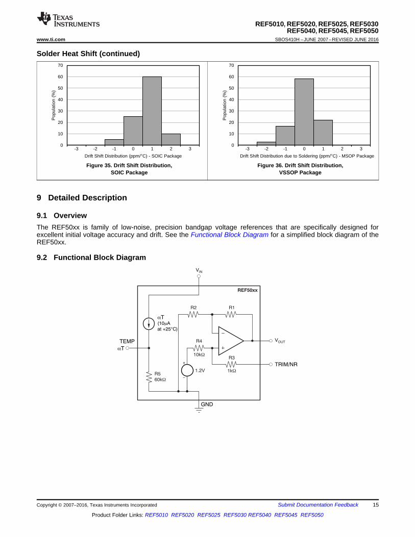
Solder Heat Shift (continued)
Figure 35. Drift Shift Distribution,SOIC Package
Figure 36. Drift Shift Distribution,VSSOP Package
9 Detailed Description
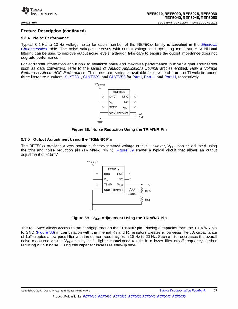
9.1 OverviewThe REF50xx is family of low-noise, precision bandgap voltage references that are specifically designed forexcellent initial voltage accuracy and drift. See the Functional Block Diagram for a simplified block diagram of theREF50xx.
9.2 Functional Block Diagram

PRE POST 6HYST
NOM
V VV 10 (ppm)
V
æ ö-= ×ç ÷ç ÷
è ø
DriftVOUTMAX VOUTMIN
VOUT Temp Range106(ppm)= ( –
× ) ×
DNC
TEMP VOUT
VIN
GND
DNC
NC
TRIM/NR
REF50xx
VTEMP
2.6mV/ C°OPA
(1)
NOTE: (1) Low drift op amp, such as the OPA333, OPA335, or OPA376.
+V
16
REF5010, REF5020, REF5025, REF5030REF5040, REF5045, REF5050SBOS410H –JUNE 2007–REVISED JUNE 2016 www.ti.com
Product Folder Links: REF5010 REF5020 REF5025 REF5030 REF5040 REF5045 REF5050
Submit Documentation Feedback Copyright © 2007–2016, Texas Instruments Incorporated
9.3 Feature Description
9.3.1 Temperature MonitoringThe temperature output terminal (TEMP, pin 3) provides a temperature-dependent voltage output withapproximately 60-kΩ source impedance. As illustrated in Figure 8, the output voltage follows the nominalrelationship:
VTEMP PIN = 509 mV + 2.64 × T(°C) (1)
This pin indicates general chip temperature, accurate to approximately ±15°C. Although not generally suitable foraccurate temperature measurements, this pin can be used to indicate temperature changes or for temperaturecompensation of analog circuitry. A temperature change of 30°C corresponds to an approximate 79-mV changein voltage at the TEMP pin.
The TEMP pin has high-output impedance (see the Functional Block Diagram). Loading this pin with a low-impedance circuit induces a measurement error; however, this pin does not have any effect on VOUT accuracy.
To avoid errors caused by low-impedance loading, buffer the TEMP pin output with a suitable low-temperaturedrift op amp, such as the OPA333, OPA335, or OPA376, as shown in Figure 37.
Figure 37. Buffering the TEMP Pin Output
9.3.2 Temperature DriftThe REF50xx is designed for minimal drift error, which is defined as the change in output voltage overtemperature. The drift is calculated using the box method, as described in Equation 2.
(2)
The REF50xx features a maximum drift coefficient of 3 ppm/°C for the high-grade version, and 8 ppm/°C for thestandard-grade.
9.3.3 Thermal HysteresisThermal hysteresis for the REF50xx is defined as the change in output voltage after operating the device at25°C, cycling the device through the specified temperature range, and returning to 25°C. Thermal hysteresis canbe expressed as Equation 3:
where• VHYST = thermal hysteresis (in units of ppm).• VNOM = the specified output voltage.• VPRE = output voltage measured at 25°C pretemperature cycling.• VPOST = output voltage measured after the device has been cycled from 25°C through the specified temperature
range of –40°C to 125°C and returned to 25°C. (3)
DNC
TEMP VOUT
VIN
GND
DNC
NC
TRIM/NR
REF50xx
+VSUPPLY
10kW
1kW
470kW
DNC
TEMP VOUT
VIN
GND
DNC
NC
TRIM/NR
REF50xx
C1
1 Fm
+VSUPPLY
17
REF5010, REF5020, REF5025, REF5030REF5040, REF5045, REF5050
www.ti.com SBOS410H –JUNE 2007–REVISED JUNE 2016
Product Folder Links: REF5010 REF5020 REF5025 REF5030 REF5040 REF5045 REF5050
Submit Documentation FeedbackCopyright © 2007–2016, Texas Instruments Incorporated
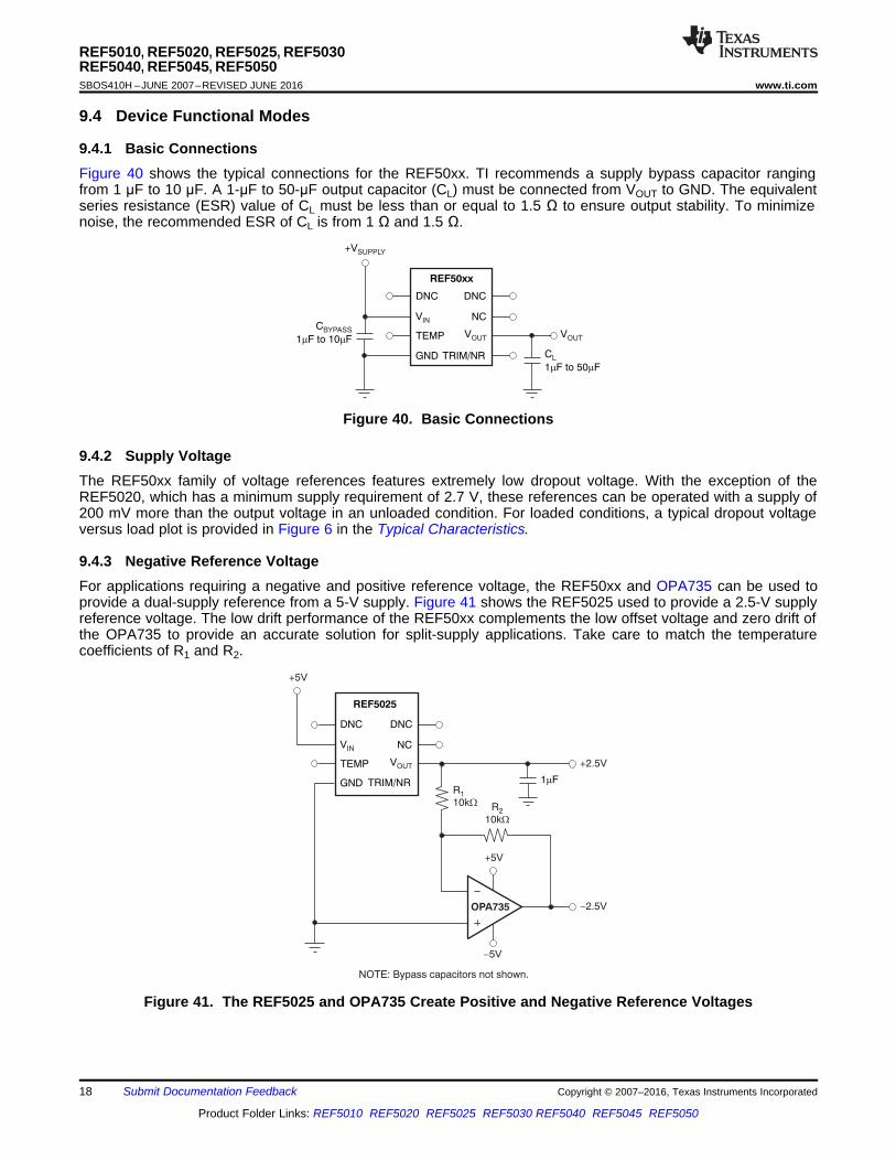
Feature Description (continued)9.3.4 Noise PerformanceTypical 0.1-Hz to 10-Hz voltage noise for each member of the REF50xx family is specified in the ElectricalCharacteristics table. The noise voltage increases with output voltage and operating temperature. Additionalfiltering can be used to improve output noise levels, although take care to ensure the output impedance does notdegrade performance.
For additional information about how to minimize noise and maximize performance in mixed-signal applicationssuch as data converters, refer to the series of Analog Applications Journal articles entitled, How a VoltageReference Affects ADC Performance. This three-part series is available for download from the TI website underthree literature numbers: SLYT331, SLYT339, and SLYT355 for Part I, Part II, and Part III, respectively.
Figure 38. Noise Reduction Using the TRIM/NR Pin
9.3.5 Output Adjustment Using the TRIM/NR PinThe REF50xx provides a very accurate, factory-trimmed voltage output. However, VOUT can be adjusted usingthe trim and noise reduction pin (TRIM/NR, pin 5). Figure 39 shows a typical circuit that allows an outputadjustment of ±15mV
Figure 39. VOUT Adjustment Using the TRIM/NR Pin
The REF50xx allows access to the bandgap through the TRIM/NR pin. Placing a capacitor from the TRIM/NR pinto GND (Figure 38) in combination with the internal R3 and R4 resistors creates a low-pass filter. A capacitanceof 1μF creates a low-pass filter with the corner frequency from 10 Hz to 20 Hz. Such a filter decreases the overallnoise measured on the VOUT pin by half. Higher capacitance results in a lower filter cutoff frequency, furtherreducing output noise. Using this capacitor increases start-up time.
-2.5V
+2.5V
+5V
NOTE: Bypass capacitors not shown.
R1
10kW R2
10kW
-5V
OPA735
+5V
DNC
TEMP VOUT
VIN
GND
DNC
NC
TRIM/NR
REF5025
1 Fm
DNC
TEMP VOUT
VIN
GND
DNC
NC
TRIM/NR
REF50xx
CBYPASS
1 F to 10 Fm m
CL
1 F to 50 Fm m
+VSUPPLY
VOUT
18
REF5010, REF5020, REF5025, REF5030REF5040, REF5045, REF5050SBOS410H –JUNE 2007–REVISED JUNE 2016 www.ti.com
Product Folder Links: REF5010 REF5020 REF5025 REF5030 REF5040 REF5045 REF5050
Submit Documentation Feedback Copyright © 2007–2016, Texas Instruments Incorporated
9.4 Device Functional Modes
9.4.1 Basic ConnectionsFigure 40 shows the typical connections for the REF50xx. TI recommends a supply bypass capacitor rangingfrom 1 μF to 10 μF. A 1-μF to 50-μF output capacitor (CL) must be connected from VOUT to GND. The equivalentseries resistance (ESR) value of CL must be less than or equal to 1.5 Ω to ensure output stability. To minimizenoise, the recommended ESR of CL is from 1 Ω and 1.5 Ω.
Figure 40. Basic Connections
9.4.2 Supply VoltageThe REF50xx family of voltage references features extremely low dropout voltage. With the exception of theREF5020, which has a minimum supply requirement of 2.7 V, these references can be operated with a supply of200 mV more than the output voltage in an unloaded condition. For loaded conditions, a typical dropout voltageversus load plot is provided in Figure 6 in the Typical Characteristics.
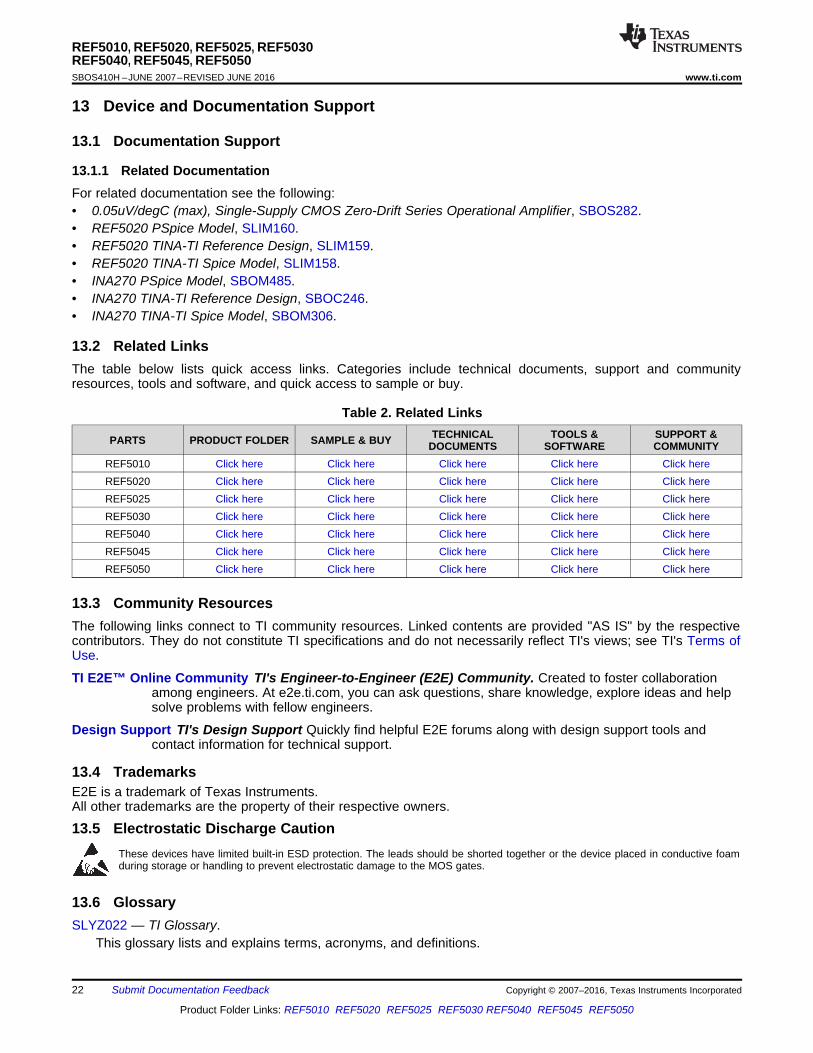
9.4.3 Negative Reference VoltageFor applications requiring a negative and positive reference voltage, the REF50xx and OPA735 can be used toprovide a dual-supply reference from a 5-V supply. Figure 41 shows the REF5025 used to provide a 2.5-V supplyreference voltage. The low drift performance of the REF50xx complements the low offset voltage and zero drift ofthe OPA735 to provide an accurate solution for split-supply applications. Take care to match the temperaturecoefficients of R1 and R2.
Figure 41. The REF5025 and OPA735 Create Positive and Negative Reference Voltages

ADS8326
REF5040
OPA365
ESR
47µF
10µF
REFIN
CS
CLK
SDO
1nF
0-4V
124
19
REF5010, REF5020, REF5025, REF5030REF5040, REF5045, REF5050
www.ti.com SBOS410H –JUNE 2007–REVISED JUNE 2016
Product Folder Links: REF5010 REF5020 REF5025 REF5030 REF5040 REF5045 REF5050
Submit Documentation FeedbackCopyright © 2007–2016, Texas Instruments Incorporated
10 Applications and Implementation
NOTEInformation in the following applications sections is not part of the TI componentspecification, and TI does not warrant its accuracy or completeness. TI’s customers areresponsible for determining suitability of components for their purposes. Customers shouldvalidate and test their design implementation to confirm system functionality.
10.1 Application InformationData acquisition systems often require stable voltage references to maintain accuracy. The REF50xx familyfeatures low noise, very low drift, and high initial accuracy for high-performance data converters. Figure 42shows the REF5040 in a basic data acquisition system.
10.2 Typical Applications
10.2.1 16-bit, 250-KSPS Data Acquisition System
Figure 42. Complete Data Acquisition System Using REF50xx
10.2.1.1 Design RequirementsWhen using the REF50xx in the design, select a proper output capacitor that does not create gain peaking,thereby increasing total system noise. At the same time, the capacitor must be selected to provide requiredfiltering performance for the system. In addition, input bypass capacitor and noise reduction capacitors must beadded for optimum performances. During the design of the data acquisition system, equal consideration must begiven to the buffering analog input signal as well as the reference voltage. Having a properly designed inputbuffer with an associated RC filter is a necessary requirement for good performance of the Data AcquisitionSystem.
10.2.1.2 Detailed Design ProcedureThe OPA365 is used to drive the 16-bit Analog to Digital Converter (ADS8326). The RC filter at the output of theOPA365 is used to reduce the charge kick-back created by the opening and closing of the sampling switch insidethe ADC. Design the RC filter such that the voltage at the sampling capacitor settles to 16-bit accuracy within theacquisition time of the ADC. The bandwidth of the driving amplifier must at least be 4 times the bandwidth of theRC filter.

20
REF5010, REF5020, REF5025, REF5030REF5040, REF5045, REF5050SBOS410H –JUNE 2007–REVISED JUNE 2016 www.ti.com
Product Folder Links: REF5010 REF5020 REF5025 REF5030 REF5040 REF5045 REF5050
Submit Documentation Feedback Copyright © 2007–2016, Texas Instruments Incorporated
Typical Applications (continued)The REF5040 is used to drive the REF pin of the ADS8326. Proper selection of Voltage Reference outputcapacitor is very important for this design. Very Low equivalent series resistance (ESR) creates gain-peakingwhich degrades SNR of the total system. If the ESR of the capacitor is not enough, then an additional resistormust be added in series with the output capacitor. A capacitance of 1 μF can be connected to the NR pin toreduce bandgap noise of the REF50xx.
SNR Measurements using different RC filters at the output of OPA365, different values of output capacitor for theREF50xx and different values of capacitors at the TRIM/NR pin are shown in Table 1.
Table 1. Data Acquisition Measurement Results for Different ConditionsTEST CONDITION 1 TEST CONDITION 2
OPA365 RC filter 124 Ω, 1 nF 124 Ω, 1 nFREF5040 Output capacitor 10 μF 10 μF + 47 μF
TRIM /NR pin capacitor 0 μF 1 μFSNR 86.7 dB 92.8 dB
10.2.1.3 Application Curve
Figure 43. FFT plot- Noise floor of Data Acquisition system

RE
F50
xx
DNC
VIN
TEMP
GND
DNC
NC
VOUT
TRIM/NR
C
C
R
C C
21
REF5010, REF5020, REF5025, REF5030REF5040, REF5045, REF5050
www.ti.com SBOS410H –JUNE 2007–REVISED JUNE 2016
Product Folder Links: REF5010 REF5020 REF5025 REF5030 REF5040 REF5045 REF5050
Submit Documentation FeedbackCopyright © 2007–2016, Texas Instruments Incorporated
11 Power Supply RecommendationsThe REF50xx family of voltage references features extremely low dropout voltage. With the exception of theREF5020, which has a minimum supply requirement of 2.7 V, these references can be operated with a supply of200 mV more than the output voltage in an unloaded condition. For loaded conditions, a typical dropout voltageversus load plot is provided in Figure 6 in the Typical Characteristics. TI recommends a supply bypass capacitorranging from 1 μF to 50 μF.
12 Layout
12.1 Layout Guidelines• Place the power-supply bypass capacitor as closely as possible to the supply and ground pins. The
recommended value of this bypass capacitor is from 1 μF to 10 μF. If necessary, additional decouplingcapacitance can be added to compensate for noisy or high-impedance power supplies.
• Place a 1-μF noise filtering capacitor between the NR pin and ground.• The output must be decoupled with a 1-μF to 50-μF capacitor. A resistor in series with the output capacitor is
optional. For better noise performance, the recommended ESR on the output capacitor is from 1 Ω to 1.5 Ω.• A high-frequency, 1-μF capacitor can be added in parallel between the output and ground to filter noise and
help with switching loads as data converters.
12.2 Layout Example
Figure 44. Layout Example
12.3 Power DissipationThe REF50xx family is specified to deliver current loads of ±10 mA over the specified input voltage range. Thetemperature of the device increases according to Equation 4:
TJ = TA + PD × θJA
where• TJ = Junction temperature (°C)• TA = Ambient temperature (°C)• PD = Power dissipated (W)• θJA = Junction-to-ambient thermal resistance (°C/W) (4)
The REF50xx junction temperature must not exceed the absolute maximum rating of 150°C.
22
REF5010, REF5020, REF5025, REF5030REF5040, REF5045, REF5050SBOS410H –JUNE 2007–REVISED JUNE 2016 www.ti.com
Product Folder Links: REF5010 REF5020 REF5025 REF5030 REF5040 REF5045 REF5050
Submit Documentation Feedback Copyright © 2007–2016, Texas Instruments Incorporated
13 Device and Documentation Support
13.1 Documentation Support
13.1.1 Related DocumentationFor related documentation see the following:• 0.05uV/degC (max), Single-Supply CMOS Zero-Drift Series Operational Amplifier, SBOS282.• REF5020 PSpice Model, SLIM160.• REF5020 TINA-TI Reference Design, SLIM159.• REF5020 TINA-TI Spice Model, SLIM158.• INA270 PSpice Model, SBOM485.• INA270 TINA-TI Reference Design, SBOC246.• INA270 TINA-TI Spice Model, SBOM306.
13.2 Related LinksThe table below lists quick access links. Categories include technical documents, support and communityresources, tools and software, and quick access to sample or buy.
Table 2. Related Links
PARTS PRODUCT FOLDER SAMPLE & BUY TECHNICALDOCUMENTS
TOOLS &SOFTWARE
SUPPORT &COMMUNITY
REF5010 Click here Click here Click here Click here Click hereREF5020 Click here Click here Click here Click here Click hereREF5025 Click here Click here Click here Click here Click hereREF5030 Click here Click here Click here Click here Click hereREF5040 Click here Click here Click here Click here Click hereREF5045 Click here Click here Click here Click here Click hereREF5050 Click here Click here Click here Click here Click here
13.3 Community ResourcesThe following links connect to TI community resources. Linked contents are provided "AS IS" by the respectivecontributors. They do not constitute TI specifications and do not necessarily reflect TI's views; see TI's Terms ofUse.
TI E2E™ Online Community TI's Engineer-to-Engineer (E2E) Community. Created to foster collaborationamong engineers. At e2e.ti.com, you can ask questions, share knowledge, explore ideas and helpsolve problems with fellow engineers.
Design Support TI's Design Support Quickly find helpful E2E forums along with design support tools andcontact information for technical support.
13.4 TrademarksE2E is a trademark of Texas Instruments.All other trademarks are the property of their respective owners.
13.5 Electrostatic Discharge CautionThese devices have limited built-in ESD protection. The leads should be shorted together or the device placed in conductive foamduring storage or handling to prevent electrostatic damage to the MOS gates.
13.6 GlossarySLYZ022 — TI Glossary.
This glossary lists and explains terms, acronyms, and definitions.

23
REF5010, REF5020, REF5025, REF5030REF5040, REF5045, REF5050
www.ti.com SBOS410H –JUNE 2007–REVISED JUNE 2016
Product Folder Links: REF5010 REF5020 REF5025 REF5030 REF5040 REF5045 REF5050
Submit Documentation FeedbackCopyright © 2007–2016, Texas Instruments Incorporated
14 Mechanical, Packaging, and Orderable InformationThe following pages include mechanical, packaging, and orderable information. This information is the mostcurrent data available for the designated devices. This data is subject to change without notice and revision ofthis document. For browser-based versions of this data sheet, refer to the left-hand navigation.

PACKAGE OPTION ADDENDUM
www.ti.com 22-Aug-2017
Addendum-Page 1
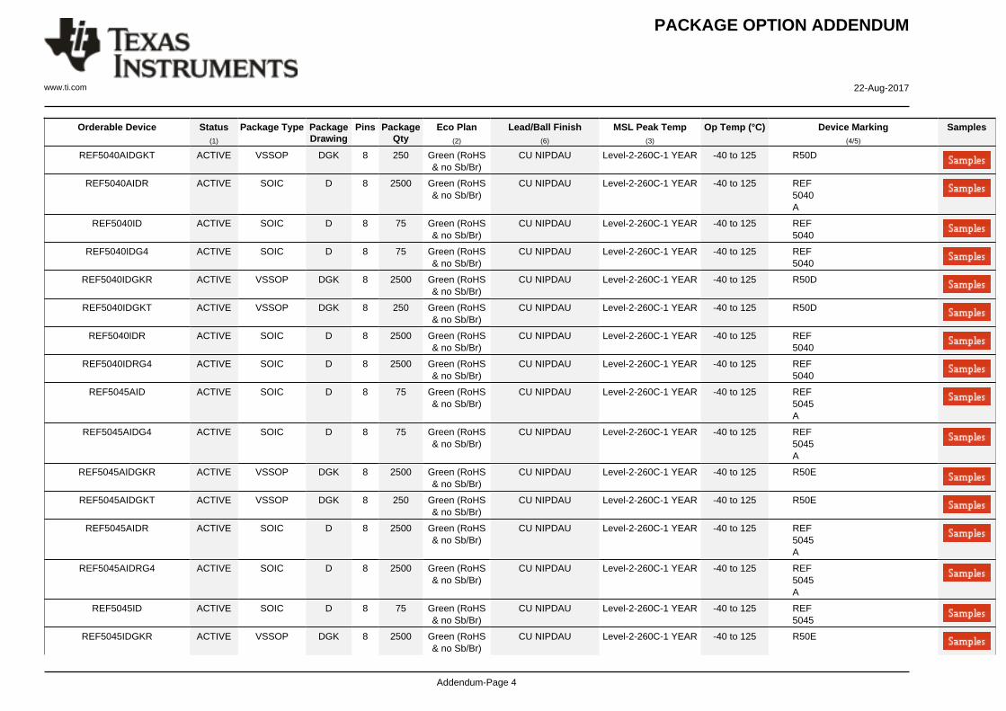
PACKAGING INFORMATION
Orderable Device Status(1)
Package Type PackageDrawing
Pins PackageQty
Eco Plan(2)
Lead/Ball Finish(6)
MSL Peak Temp(3)
Op Temp (°C) Device Marking(4/5)
Samples
REF5010AID ACTIVE SOIC D 8 75 Green (RoHS& no Sb/Br)
CU NIPDAU Level-2-260C-1 YEAR -40 to 125 REF5010A
REF5010AIDGKR ACTIVE VSSOP DGK 8 2500 Green (RoHS& no Sb/Br)
CU NIPDAU Level-2-260C-1 YEAR -40 to 125 R50G
REF5010AIDGKT ACTIVE VSSOP DGK 8 250 Green (RoHS& no Sb/Br)
CU NIPDAU Level-2-260C-1 YEAR -40 to 125 R50G
REF5010AIDR ACTIVE SOIC D 8 2500 Green (RoHS& no Sb/Br)
CU NIPDAU Level-2-260C-1 YEAR -40 to 125 REF5010A
REF5010ID ACTIVE SOIC D 8 75 Green (RoHS& no Sb/Br)
CU NIPDAU Level-2-260C-1 YEAR -40 to 125 REF5010
REF5010IDGKR ACTIVE VSSOP DGK 8 2500 Green (RoHS& no Sb/Br)
CU NIPDAU Level-2-260C-1 YEAR -40 to 125 R50G
REF5010IDGKT ACTIVE VSSOP DGK 8 250 Green (RoHS& no Sb/Br)
CU NIPDAU Level-2-260C-1 YEAR -40 to 125 R50G
REF5020AID ACTIVE SOIC D 8 75 Green (RoHS& no Sb/Br)
CU NIPDAU Level-2-260C-1 YEAR -40 to 125 REF5020A
REF5020AIDG4 ACTIVE SOIC D 8 75 Green (RoHS& no Sb/Br)
CU NIPDAU Level-2-260C-1 YEAR -40 to 125 REF5020A
REF5020AIDGKR ACTIVE VSSOP DGK 8 2500 Green (RoHS& no Sb/Br)
CU NIPDAU Level-2-260C-1 YEAR -40 to 125 R50A
REF5020AIDGKT ACTIVE VSSOP DGK 8 250 Green (RoHS& no Sb/Br)
CU NIPDAU Level-2-260C-1 YEAR -40 to 125 R50A
REF5020AIDR ACTIVE SOIC D 8 2500 Green (RoHS& no Sb/Br)
CU NIPDAU Level-2-260C-1 YEAR -40 to 125 REF5020A
REF5020AIDRG4 ACTIVE SOIC D 8 2500 Green (RoHS& no Sb/Br)
CU NIPDAU Level-2-260C-1 YEAR -40 to 125 REF5020A
REF5020ID ACTIVE SOIC D 8 75 Green (RoHS& no Sb/Br)
CU NIPDAU Level-2-260C-1 YEAR -40 to 125 REF5020

PACKAGE OPTION ADDENDUM
www.ti.com 22-Aug-2017
Addendum-Page 2
Orderable Device Status(1)
Package Type PackageDrawing
Pins PackageQty
Eco Plan(2)
Lead/Ball Finish(6)
MSL Peak Temp(3)
Op Temp (°C) Device Marking(4/5)
Samples
REF5020IDG4 ACTIVE SOIC D 8 75 Green (RoHS& no Sb/Br)
CU NIPDAU Level-2-260C-1 YEAR -40 to 125 REF5020
REF5020IDGKR ACTIVE VSSOP DGK 8 2500 Green (RoHS& no Sb/Br)
CU NIPDAU Level-2-260C-1 YEAR -40 to 125 R50A
REF5020IDGKT ACTIVE VSSOP DGK 8 250 Green (RoHS& no Sb/Br)
CU NIPDAU Level-2-260C-1 YEAR -40 to 125 R50A
REF5020IDR ACTIVE SOIC D 8 2500 Green (RoHS& no Sb/Br)
CU NIPDAU Level-2-260C-1 YEAR -40 to 125 REF5020
REF5020IDRG4 ACTIVE SOIC D 8 2500 Green (RoHS& no Sb/Br)
CU NIPDAU Level-2-260C-1 YEAR -40 to 125 REF5020
REF5025AID ACTIVE SOIC D 8 75 Green (RoHS& no Sb/Br)
CU NIPDAU Level-2-260C-1 YEAR -40 to 125 REF5025A
REF5025AIDG4 ACTIVE SOIC D 8 75 Green (RoHS& no Sb/Br)
CU NIPDAU Level-2-260C-1 YEAR -40 to 125 REF5025A
REF5025AIDGKR ACTIVE VSSOP DGK 8 2500 Green (RoHS& no Sb/Br)
CU NIPDAU Level-2-260C-1 YEAR -40 to 125 R50B
REF5025AIDGKT ACTIVE VSSOP DGK 8 250 Green (RoHS& no Sb/Br)
CU NIPDAU Level-2-260C-1 YEAR -40 to 125 R50B
REF5025AIDR ACTIVE SOIC D 8 2500 Green (RoHS& no Sb/Br)
CU NIPDAU Level-2-260C-1 YEAR -40 to 125 REF5025A
REF5025AIDRG4 ACTIVE SOIC D 8 2500 Green (RoHS& no Sb/Br)
CU NIPDAU Level-2-260C-1 YEAR -40 to 125 REF5025A
REF5025ID ACTIVE SOIC D 8 75 Green (RoHS& no Sb/Br)
CU NIPDAU Level-2-260C-1 YEAR -40 to 125 REF5025
REF5025IDG4 ACTIVE SOIC D 8 75 Green (RoHS& no Sb/Br)
CU NIPDAU Level-2-260C-1 YEAR -40 to 125 REF5025
REF5025IDGKR ACTIVE VSSOP DGK 8 2500 Green (RoHS& no Sb/Br)
CU NIPDAU Level-2-260C-1 YEAR -40 to 125 R50B
REF5025IDGKT ACTIVE VSSOP DGK 8 250 Green (RoHS& no Sb/Br)
CU NIPDAU Level-2-260C-1 YEAR -40 to 125 R50B
REF5025IDR ACTIVE SOIC D 8 2500 Green (RoHS& no Sb/Br)
CU NIPDAU Level-2-260C-1 YEAR -40 to 125 REF5025

PACKAGE OPTION ADDENDUM
www.ti.com 22-Aug-2017
Addendum-Page 3
Orderable Device Status(1)
Package Type PackageDrawing
Pins PackageQty
Eco Plan(2)
Lead/Ball Finish(6)
MSL Peak Temp(3)
Op Temp (°C) Device Marking(4/5)
Samples
REF5025IDRG4 ACTIVE SOIC D 8 2500 Green (RoHS& no Sb/Br)
CU NIPDAU Level-2-260C-1 YEAR -40 to 125 REF5025
REF5030AID ACTIVE SOIC D 8 75 Green (RoHS& no Sb/Br)
CU NIPDAU Level-2-260C-1 YEAR -40 to 125 REF5030A
REF5030AIDG4 ACTIVE SOIC D 8 75 Green (RoHS& no Sb/Br)
CU NIPDAU Level-2-260C-1 YEAR -40 to 125 REF5030A
REF5030AIDGKR ACTIVE VSSOP DGK 8 2500 Green (RoHS& no Sb/Br)
CU NIPDAU Level-2-260C-1 YEAR -40 to 125 R50C
REF5030AIDGKT ACTIVE VSSOP DGK 8 250 Green (RoHS& no Sb/Br)
CU NIPDAU Level-2-260C-1 YEAR -40 to 125 R50C
REF5030AIDR ACTIVE SOIC D 8 2500 Green (RoHS& no Sb/Br)
CU NIPDAU Level-2-260C-1 YEAR -40 to 125 REF5030A
REF5030AIDRG4 ACTIVE SOIC D 8 2500 Green (RoHS& no Sb/Br)
CU NIPDAU Level-2-260C-1 YEAR -40 to 125 REF5030A
REF5030ID ACTIVE SOIC D 8 75 Green (RoHS& no Sb/Br)
CU NIPDAU Level-2-260C-1 YEAR -40 to 125 REF5030
REF5030IDG4 ACTIVE SOIC D 8 75 Green (RoHS& no Sb/Br)
CU NIPDAU Level-2-260C-1 YEAR -40 to 125 REF5030
REF5030IDGKR ACTIVE VSSOP DGK 8 2500 Green (RoHS& no Sb/Br)
CU NIPDAU Level-2-260C-1 YEAR -40 to 125 R50C
REF5030IDGKT ACTIVE VSSOP DGK 8 250 Green (RoHS& no Sb/Br)
CU NIPDAU Level-2-260C-1 YEAR -40 to 125 R50C
REF5030IDR ACTIVE SOIC D 8 2500 Green (RoHS& no Sb/Br)
CU NIPDAU Level-2-260C-1 YEAR -40 to 125 REF5030
REF5040AID ACTIVE SOIC D 8 75 Green (RoHS& no Sb/Br)
CU NIPDAU Level-2-260C-1 YEAR -40 to 125 REF5040A
REF5040AIDG4 ACTIVE SOIC D 8 75 Green (RoHS& no Sb/Br)
CU NIPDAU Level-2-260C-1 YEAR -40 to 125 REF5040A
REF5040AIDGKR ACTIVE VSSOP DGK 8 2500 Green (RoHS& no Sb/Br)
CU NIPDAU Level-2-260C-1 YEAR -40 to 125 R50D
PACKAGE OPTION ADDENDUM
www.ti.com 22-Aug-2017
Addendum-Page 4
Orderable Device Status(1)
Package Type PackageDrawing
Pins PackageQty
Eco Plan(2)
Lead/Ball Finish(6)
MSL Peak Temp(3)
Op Temp (°C) Device Marking(4/5)
Samples
REF5040AIDGKT ACTIVE VSSOP DGK 8 250 Green (RoHS& no Sb/Br)
CU NIPDAU Level-2-260C-1 YEAR -40 to 125 R50D
REF5040AIDR ACTIVE SOIC D 8 2500 Green (RoHS& no Sb/Br)
CU NIPDAU Level-2-260C-1 YEAR -40 to 125 REF5040A
REF5040ID ACTIVE SOIC D 8 75 Green (RoHS& no Sb/Br)
CU NIPDAU Level-2-260C-1 YEAR -40 to 125 REF5040
REF5040IDG4 ACTIVE SOIC D 8 75 Green (RoHS& no Sb/Br)
CU NIPDAU Level-2-260C-1 YEAR -40 to 125 REF5040
REF5040IDGKR ACTIVE VSSOP DGK 8 2500 Green (RoHS& no Sb/Br)
CU NIPDAU Level-2-260C-1 YEAR -40 to 125 R50D
REF5040IDGKT ACTIVE VSSOP DGK 8 250 Green (RoHS& no Sb/Br)
CU NIPDAU Level-2-260C-1 YEAR -40 to 125 R50D
REF5040IDR ACTIVE SOIC D 8 2500 Green (RoHS& no Sb/Br)
CU NIPDAU Level-2-260C-1 YEAR -40 to 125 REF5040
REF5040IDRG4 ACTIVE SOIC D 8 2500 Green (RoHS& no Sb/Br)
CU NIPDAU Level-2-260C-1 YEAR -40 to 125 REF5040
REF5045AID ACTIVE SOIC D 8 75 Green (RoHS& no Sb/Br)
CU NIPDAU Level-2-260C-1 YEAR -40 to 125 REF5045A
REF5045AIDG4 ACTIVE SOIC D 8 75 Green (RoHS& no Sb/Br)
CU NIPDAU Level-2-260C-1 YEAR -40 to 125 REF5045A
REF5045AIDGKR ACTIVE VSSOP DGK 8 2500 Green (RoHS& no Sb/Br)
CU NIPDAU Level-2-260C-1 YEAR -40 to 125 R50E
REF5045AIDGKT ACTIVE VSSOP DGK 8 250 Green (RoHS& no Sb/Br)
CU NIPDAU Level-2-260C-1 YEAR -40 to 125 R50E
REF5045AIDR ACTIVE SOIC D 8 2500 Green (RoHS& no Sb/Br)
CU NIPDAU Level-2-260C-1 YEAR -40 to 125 REF5045A
REF5045AIDRG4 ACTIVE SOIC D 8 2500 Green (RoHS& no Sb/Br)
CU NIPDAU Level-2-260C-1 YEAR -40 to 125 REF5045A
REF5045ID ACTIVE SOIC D 8 75 Green (RoHS& no Sb/Br)
CU NIPDAU Level-2-260C-1 YEAR -40 to 125 REF5045
REF5045IDGKR ACTIVE VSSOP DGK 8 2500 Green (RoHS& no Sb/Br)
CU NIPDAU Level-2-260C-1 YEAR -40 to 125 R50E
PACKAGE OPTION ADDENDUM
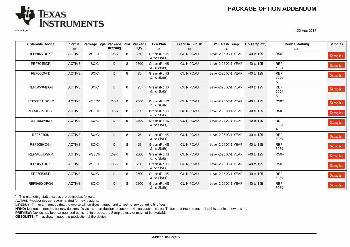
www.ti.com 22-Aug-2017
Addendum-Page 5
Orderable Device Status(1)
Package Type PackageDrawing
Pins PackageQty
Eco Plan(2)
Lead/Ball Finish(6)
MSL Peak Temp(3)
Op Temp (°C) Device Marking(4/5)
Samples
REF5045IDGKT ACTIVE VSSOP DGK 8 250 Green (RoHS& no Sb/Br)
CU NIPDAU Level-2-260C-1 YEAR -40 to 125 R50E
REF5045IDR ACTIVE SOIC D 8 2500 Green (RoHS& no Sb/Br)
CU NIPDAU Level-2-260C-1 YEAR -40 to 125 REF5045
REF5050AID ACTIVE SOIC D 8 75 Green (RoHS& no Sb/Br)
CU NIPDAU Level-2-260C-1 YEAR -40 to 125 REF5050A
REF5050AIDG4 ACTIVE SOIC D 8 75 Green (RoHS& no Sb/Br)
CU NIPDAU Level-2-260C-1 YEAR -40 to 125 REF5050A
REF5050AIDGKR ACTIVE VSSOP DGK 8 2500 Green (RoHS& no Sb/Br)
CU NIPDAU Level-2-260C-1 YEAR -40 to 125 R50F
REF5050AIDGKT ACTIVE VSSOP DGK 8 250 Green (RoHS& no Sb/Br)
CU NIPDAU Level-2-260C-1 YEAR -40 to 125 R50F
REF5050AIDR ACTIVE SOIC D 8 2500 Green (RoHS& no Sb/Br)
CU NIPDAU Level-2-260C-1 YEAR -40 to 125 REF5050A
REF5050ID ACTIVE SOIC D 8 75 Green (RoHS& no Sb/Br)
CU NIPDAU Level-2-260C-1 YEAR -40 to 125 REF5050
REF5050IDG4 ACTIVE SOIC D 8 75 Green (RoHS& no Sb/Br)
CU NIPDAU Level-2-260C-1 YEAR -40 to 125 REF5050
REF5050IDGKR ACTIVE VSSOP DGK 8 2500 Green (RoHS& no Sb/Br)
CU NIPDAU Level-2-260C-1 YEAR -40 to 125 R50F
REF5050IDGKT ACTIVE VSSOP DGK 8 250 Green (RoHS& no Sb/Br)
CU NIPDAU Level-2-260C-1 YEAR -40 to 125 R50F
REF5050IDR ACTIVE SOIC D 8 2500 Green (RoHS& no Sb/Br)
CU NIPDAU Level-2-260C-1 YEAR -40 to 125 REF5050
REF5050IDRG4 ACTIVE SOIC D 8 2500 Green (RoHS& no Sb/Br)
CU NIPDAU Level-2-260C-1 YEAR -40 to 125 REF5050
(1) The marketing status values are defined as follows:ACTIVE: Product device recommended for new designs.LIFEBUY: TI has announced that the device will be discontinued, and a lifetime-buy period is in effect.NRND: Not recommended for new designs. Device is in production to support existing customers, but TI does not recommend using this part in a new design.PREVIEW: Device has been announced but is not in production. Samples may or may not be available.OBSOLETE: TI has discontinued the production of the device.

PACKAGE OPTION ADDENDUM
www.ti.com 22-Aug-2017
Addendum-Page 6
(2) RoHS: TI defines "RoHS" to mean semiconductor products that are compliant with the current EU RoHS requirements for all 10 RoHS substances, including the requirement that RoHS substancedo not exceed 0.1% by weight in homogeneous materials. Where designed to be soldered at high temperatures, "RoHS" products are suitable for use in specified lead-free processes. TI mayreference these types of products as "Pb-Free".RoHS Exempt: TI defines "RoHS Exempt" to mean products that contain lead but are compliant with EU RoHS pursuant to a specific EU RoHS exemption.Green: TI defines "Green" to mean the content of Chlorine (Cl) and Bromine (Br) based flame retardants meet JS709B low halogen requirements of <=1000ppm threshold. Antimony trioxide basedflame retardants must also meet the <=1000ppm threshold requirement.
(3) MSL, Peak Temp. - The Moisture Sensitivity Level rating according to the JEDEC industry standard classifications, and peak solder temperature.
(4) There may be additional marking, which relates to the logo, the lot trace code information, or the environmental category on the device.
(5) Multiple Device Markings will be inside parentheses. Only one Device Marking contained in parentheses and separated by a "~" will appear on a device. If a line is indented then it is a continuationof the previous line and the two combined represent the entire Device Marking for that device.
(6) Lead/Ball Finish - Orderable Devices may have multiple material finish options. Finish options are separated by a vertical ruled line. Lead/Ball Finish values may wrap to two lines if the finishvalue exceeds the maximum column width.
Important Information and Disclaimer:The information provided on this page represents TI's knowledge and belief as of the date that it is provided. TI bases its knowledge and belief on informationprovided by third parties, and makes no representation or warranty as to the accuracy of such information. Efforts are underway to better integrate information from third parties. TI has taken andcontinues to take reasonable steps to provide representative and accurate information but may not have conducted destructive testing or chemical analysis on incoming materials and chemicals.TI and TI suppliers consider certain information to be proprietary, and thus CAS numbers and other limited information may not be available for release.
In no event shall TI's liability arising out of such information exceed the total purchase price of the TI part(s) at issue in this document sold by TI to Customer on an annual basis.
OTHER QUALIFIED VERSIONS OF REF5020, REF5025, REF5040, REF5050 :
• Enhanced Product: REF5020-EP, REF5025-EP, REF5040-EP, REF5050-EP
NOTE: Qualified Version Definitions:
• Enhanced Product - Supports Defense, Aerospace and Medical Applications

TAPE AND REEL INFORMATION
*All dimensions are nominal
Device PackageType
PackageDrawing
Pins SPQ ReelDiameter
(mm)
ReelWidth
W1 (mm)
A0(mm)
B0(mm)
K0(mm)
P1(mm)
W(mm)
Pin1Quadrant
REF5010AIDGKR VSSOP DGK 8 2500 330.0 12.4 5.3 3.4 1.4 8.0 12.0 Q1
REF5010AIDGKT VSSOP DGK 8 250 180.0 12.4 5.3 3.4 1.4 8.0 12.0 Q1
REF5010AIDR SOIC D 8 2500 330.0 12.4 6.4 5.2 2.1 8.0 12.0 Q1
REF5010IDGKR VSSOP DGK 8 2500 330.0 12.4 5.3 3.4 1.4 8.0 12.0 Q1
REF5010IDGKT VSSOP DGK 8 250 180.0 12.4 5.3 3.4 1.4 8.0 12.0 Q1
REF5020AIDGKR VSSOP DGK 8 2500 330.0 12.4 5.3 3.4 1.4 8.0 12.0 Q1
REF5020AIDGKT VSSOP DGK 8 250 180.0 12.4 5.3 3.4 1.4 8.0 12.0 Q1
REF5020AIDR SOIC D 8 2500 330.0 12.4 6.4 5.2 2.1 8.0 12.0 Q1
REF5020IDGKR VSSOP DGK 8 2500 330.0 12.4 5.3 3.4 1.4 8.0 12.0 Q1
REF5020IDGKT VSSOP DGK 8 250 180.0 12.4 5.3 3.4 1.4 8.0 12.0 Q1
REF5020IDR SOIC D 8 2500 330.0 12.4 6.4 5.2 2.1 8.0 12.0 Q1
REF5025AIDGKR VSSOP DGK 8 2500 330.0 12.4 5.3 3.4 1.4 8.0 12.0 Q1
REF5025AIDGKT VSSOP DGK 8 250 180.0 12.4 5.3 3.4 1.4 8.0 12.0 Q1
REF5025AIDR SOIC D 8 2500 330.0 12.4 6.4 5.2 2.1 8.0 12.0 Q1
REF5025IDGKR VSSOP DGK 8 2500 330.0 12.4 5.3 3.4 1.4 8.0 12.0 Q1
REF5025IDGKT VSSOP DGK 8 250 180.0 12.4 5.3 3.4 1.4 8.0 12.0 Q1
REF5025IDR SOIC D 8 2500 330.0 12.4 6.4 5.2 2.1 8.0 12.0 Q1
REF5030AIDGKR VSSOP DGK 8 2500 330.0 12.4 5.3 3.4 1.4 8.0 12.0 Q1
PACKAGE MATERIALS INFORMATION
www.ti.com 23-Aug-2017
Pack Materials-Page 1

Device PackageType
PackageDrawing
Pins SPQ ReelDiameter
(mm)
ReelWidth
W1 (mm)
A0(mm)
B0(mm)
K0(mm)
P1(mm)
W(mm)
Pin1Quadrant
REF5030AIDGKT VSSOP DGK 8 250 180.0 12.4 5.3 3.4 1.4 8.0 12.0 Q1
REF5030AIDR SOIC D 8 2500 330.0 12.4 6.4 5.2 2.1 8.0 12.0 Q1
REF5030IDGKR VSSOP DGK 8 2500 330.0 12.4 5.3 3.4 1.4 8.0 12.0 Q1
REF5030IDGKT VSSOP DGK 8 250 180.0 12.4 5.3 3.4 1.4 8.0 12.0 Q1
REF5030IDR SOIC D 8 2500 330.0 12.4 6.4 5.2 2.1 8.0 12.0 Q1
REF5040AIDGKR VSSOP DGK 8 2500 330.0 12.4 5.3 3.4 1.4 8.0 12.0 Q1
REF5040AIDGKT VSSOP DGK 8 250 180.0 12.4 5.3 3.4 1.4 8.0 12.0 Q1
REF5040AIDR SOIC D 8 2500 330.0 12.4 6.4 5.2 2.1 8.0 12.0 Q1
REF5040IDGKR VSSOP DGK 8 2500 330.0 12.4 5.3 3.4 1.4 8.0 12.0 Q1
REF5040IDGKT VSSOP DGK 8 250 180.0 12.4 5.3 3.4 1.4 8.0 12.0 Q1
REF5040IDR SOIC D 8 2500 330.0 12.4 6.4 5.2 2.1 8.0 12.0 Q1
REF5045AIDGKR VSSOP DGK 8 2500 330.0 12.4 5.3 3.4 1.4 8.0 12.0 Q1
REF5045AIDGKT VSSOP DGK 8 250 180.0 12.4 5.3 3.4 1.4 8.0 12.0 Q1
REF5045AIDR SOIC D 8 2500 330.0 12.4 6.4 5.2 2.1 8.0 12.0 Q1
REF5045IDGKR VSSOP DGK 8 2500 330.0 12.4 5.3 3.4 1.4 8.0 12.0 Q1
REF5045IDGKT VSSOP DGK 8 250 180.0 12.4 5.3 3.4 1.4 8.0 12.0 Q1
REF5045IDR SOIC D 8 2500 330.0 12.4 6.4 5.2 2.1 8.0 12.0 Q1
REF5050AIDGKR VSSOP DGK 8 2500 330.0 12.4 5.3 3.4 1.4 8.0 12.0 Q1
REF5050AIDGKT VSSOP DGK 8 250 180.0 12.4 5.3 3.4 1.4 8.0 12.0 Q1
REF5050AIDR SOIC D 8 2500 330.0 12.4 6.4 5.2 2.1 8.0 12.0 Q1
REF5050IDGKR VSSOP DGK 8 2500 330.0 12.4 5.3 3.4 1.4 8.0 12.0 Q1
REF5050IDGKT VSSOP DGK 8 250 180.0 12.4 5.3 3.4 1.4 8.0 12.0 Q1
REF5050IDR SOIC D 8 2500 330.0 12.4 6.4 5.2 2.1 8.0 12.0 Q1
PACKAGE MATERIALS INFORMATION
www.ti.com 23-Aug-2017
Pack Materials-Page 2

*All dimensions are nominal
Device Package Type Package Drawing Pins SPQ Length (mm) Width (mm) Height (mm)
REF5010AIDGKR VSSOP DGK 8 2500 367.0 367.0 35.0
REF5010AIDGKT VSSOP DGK 8 250 210.0 185.0 35.0
REF5010AIDR SOIC D 8 2500 367.0 367.0 35.0
REF5010IDGKR VSSOP DGK 8 2500 367.0 367.0 35.0
REF5010IDGKT VSSOP DGK 8 250 210.0 185.0 35.0
REF5020AIDGKR VSSOP DGK 8 2500 367.0 367.0 35.0
REF5020AIDGKT VSSOP DGK 8 250 210.0 185.0 35.0
REF5020AIDR SOIC D 8 2500 367.0 367.0 35.0
REF5020IDGKR VSSOP DGK 8 2500 367.0 367.0 35.0
REF5020IDGKT VSSOP DGK 8 250 210.0 185.0 35.0
REF5020IDR SOIC D 8 2500 367.0 367.0 35.0
REF5025AIDGKR VSSOP DGK 8 2500 367.0 367.0 35.0
REF5025AIDGKT VSSOP DGK 8 250 210.0 185.0 35.0
REF5025AIDR SOIC D 8 2500 367.0 367.0 35.0
REF5025IDGKR VSSOP DGK 8 2500 367.0 367.0 35.0
REF5025IDGKT VSSOP DGK 8 250 210.0 185.0 35.0
REF5025IDR SOIC D 8 2500 367.0 367.0 35.0
REF5030AIDGKR VSSOP DGK 8 2500 367.0 367.0 35.0
REF5030AIDGKT VSSOP DGK 8 250 210.0 185.0 35.0
REF5030AIDR SOIC D 8 2500 367.0 367.0 35.0
PACKAGE MATERIALS INFORMATION
www.ti.com 23-Aug-2017
Pack Materials-Page 3

Device Package Type Package Drawing Pins SPQ Length (mm) Width (mm) Height (mm)
REF5030IDGKR VSSOP DGK 8 2500 367.0 367.0 35.0
REF5030IDGKT VSSOP DGK 8 250 210.0 185.0 35.0
REF5030IDR SOIC D 8 2500 367.0 367.0 35.0
REF5040AIDGKR VSSOP DGK 8 2500 367.0 367.0 35.0
REF5040AIDGKT VSSOP DGK 8 250 210.0 185.0 35.0
REF5040AIDR SOIC D 8 2500 367.0 367.0 35.0
REF5040IDGKR VSSOP DGK 8 2500 367.0 367.0 35.0
REF5040IDGKT VSSOP DGK 8 250 210.0 185.0 35.0
REF5040IDR SOIC D 8 2500 367.0 367.0 35.0
REF5045AIDGKR VSSOP DGK 8 2500 367.0 367.0 35.0
REF5045AIDGKT VSSOP DGK 8 250 210.0 185.0 35.0
REF5045AIDR SOIC D 8 2500 367.0 367.0 35.0
REF5045IDGKR VSSOP DGK 8 2500 367.0 367.0 35.0
REF5045IDGKT VSSOP DGK 8 250 210.0 185.0 35.0
REF5045IDR SOIC D 8 2500 367.0 367.0 35.0
REF5050AIDGKR VSSOP DGK 8 2500 367.0 367.0 35.0
REF5050AIDGKT VSSOP DGK 8 250 210.0 185.0 35.0
REF5050AIDR SOIC D 8 2500 367.0 367.0 35.0
REF5050IDGKR VSSOP DGK 8 2500 367.0 367.0 35.0
REF5050IDGKT VSSOP DGK 8 250 210.0 185.0 35.0
REF5050IDR SOIC D 8 2500 367.0 367.0 35.0
PACKAGE MATERIALS INFORMATION
www.ti.com 23-Aug-2017
Pack Materials-Page 4


IMPORTANT NOTICE
Texas Instruments Incorporated (TI) reserves the right to make corrections, enhancements, improvements and other changes to itssemiconductor products and services per JESD46, latest issue, and to discontinue any product or service per JESD48, latest issue. Buyersshould obtain the latest relevant information before placing orders and should verify that such information is current and complete.TI’s published terms of sale for semiconductor products (http://www.ti.com/sc/docs/stdterms.htm) apply to the sale of packaged integratedcircuit products that TI has qualified and released to market. Additional terms may apply to the use or sale of other types of TI products andservices.Reproduction of significant portions of TI information in TI data sheets is permissible only if reproduction is without alteration and isaccompanied by all associated warranties, conditions, limitations, and notices. TI is not responsible or liable for such reproduceddocumentation. Information of third parties may be subject to additional restrictions. Resale of TI products or services with statementsdifferent from or beyond the parameters stated by TI for that product or service voids all express and any implied warranties for theassociated TI product or service and is an unfair and deceptive business practice. TI is not responsible or liable for any such statements.Buyers and others who are developing systems that incorporate TI products (collectively, “Designers”) understand and agree that Designersremain responsible for using their independent analysis, evaluation and judgment in designing their applications and that Designers havefull and exclusive responsibility to assure the safety of Designers' applications and compliance of their applications (and of all TI productsused in or for Designers’ applications) with all applicable regulations, laws and other applicable requirements. Designer represents that, withrespect to their applications, Designer has all the necessary expertise to create and implement safeguards that (1) anticipate dangerousconsequences of failures, (2) monitor failures and their consequences, and (3) lessen the likelihood of failures that might cause harm andtake appropriate actions. Designer agrees that prior to using or distributing any applications that include TI products, Designer willthoroughly test such applications and the functionality of such TI products as used in such applications.TI’s provision of technical, application or other design advice, quality characterization, reliability data or other services or information,including, but not limited to, reference designs and materials relating to evaluation modules, (collectively, “TI Resources”) are intended toassist designers who are developing applications that incorporate TI products; by downloading, accessing or using TI Resources in anyway, Designer (individually or, if Designer is acting on behalf of a company, Designer’s company) agrees to use any particular TI Resourcesolely for this purpose and subject to the terms of this Notice.TI’s provision of TI Resources does not expand or otherwise alter TI’s applicable published warranties or warranty disclaimers for TIproducts, and no additional obligations or liabilities arise from TI providing such TI Resources. TI reserves the right to make corrections,enhancements, improvements and other changes to its TI Resources. TI has not conducted any testing other than that specificallydescribed in the published documentation for a particular TI Resource.Designer is authorized to use, copy and modify any individual TI Resource only in connection with the development of applications thatinclude the TI product(s) identified in such TI Resource. NO OTHER LICENSE, EXPRESS OR IMPLIED, BY ESTOPPEL OR OTHERWISETO ANY OTHER TI INTELLECTUAL PROPERTY RIGHT, AND NO LICENSE TO ANY TECHNOLOGY OR INTELLECTUAL PROPERTYRIGHT OF TI OR ANY THIRD PARTY IS GRANTED HEREIN, including but not limited to any patent right, copyright, mask work right, orother intellectual property right relating to any combination, machine, or process in which TI products or services are used. Informationregarding or referencing third-party products or services does not constitute a license to use such products or services, or a warranty orendorsement thereof. Use of TI Resources may require a license from a third party under the patents or other intellectual property of thethird party, or a license from TI under the patents or other intellectual property of TI.TI RESOURCES ARE PROVIDED “AS IS” AND WITH ALL FAULTS. TI DISCLAIMS ALL OTHER WARRANTIES ORREPRESENTATIONS, EXPRESS OR IMPLIED, REGARDING RESOURCES OR USE THEREOF, INCLUDING BUT NOT LIMITED TOACCURACY OR COMPLETENESS, TITLE, ANY EPIDEMIC FAILURE WARRANTY AND ANY IMPLIED WARRANTIES OFMERCHANTABILITY, FITNESS FOR A PARTICULAR PURPOSE, AND NON-INFRINGEMENT OF ANY THIRD PARTY INTELLECTUALPROPERTY RIGHTS. TI SHALL NOT BE LIABLE FOR AND SHALL NOT DEFEND OR INDEMNIFY DESIGNER AGAINST ANY CLAIM,INCLUDING BUT NOT LIMITED TO ANY INFRINGEMENT CLAIM THAT RELATES TO OR IS BASED ON ANY COMBINATION OFPRODUCTS EVEN IF DESCRIBED IN TI RESOURCES OR OTHERWISE. IN NO EVENT SHALL TI BE LIABLE FOR ANY ACTUAL,DIRECT, SPECIAL, COLLATERAL, INDIRECT, PUNITIVE, INCIDENTAL, CONSEQUENTIAL OR EXEMPLARY DAMAGES INCONNECTION WITH OR ARISING OUT OF TI RESOURCES OR USE THEREOF, AND REGARDLESS OF WHETHER TI HAS BEENADVISED OF THE POSSIBILITY OF SUCH DAMAGES.Unless TI has explicitly designated an individual product as meeting the requirements of a particular industry standard (e.g., ISO/TS 16949and ISO 26262), TI is not responsible for any failure to meet such industry standard requirements.Where TI specifically promotes products as facilitating functional safety or as compliant with industry functional safety standards, suchproducts are intended to help enable customers to design and create their own applications that meet applicable functional safety standardsand requirements. Using products in an application does not by itself establish any safety features in the application. Designers mustensure compliance with safety-related requirements and standards applicable to their applications. Designer may not use any TI products inlife-critical medical equipment unless authorized officers of the parties have executed a special contract specifically governing such use.Life-critical medical equipment is medical equipment where failure of such equipment would cause serious bodily injury or death (e.g., lifesupport, pacemakers, defibrillators, heart pumps, neurostimulators, and implantables). Such equipment includes, without limitation, allmedical devices identified by the U.S. Food and Drug Administration as Class III devices and equivalent classifications outside the U.S.TI may expressly designate certain products as completing a particular qualification (e.g., Q100, Military Grade, or Enhanced Product).Designers agree that it has the necessary expertise to select the product with the appropriate qualification designation for their applicationsand that proper product selection is at Designers’ own risk. Designers are solely responsible for compliance with all legal and regulatoryrequirements in connection with such selection.Designer will fully indemnify TI and its representatives against any damages, costs, losses, and/or liabilities arising out of Designer’s non-compliance with the terms and provisions of this Notice.
Mailing Address: Texas Instruments, Post Office Box 655303, Dallas, Texas 75265Copyright © 2017, Texas Instruments Incorporated