low-complexity, low-area computer architectures …eprints.nottingham.ac.uk/45394/1/phd thesis 2017...
TRANSCRIPT

Kong, Jia Hao (2018) Low-complexity, low-area computer architectures for cryptographic application in resource constrained environments. PhD thesis, University of Nottingham.
Access from the University of Nottingham repository: http://eprints.nottingham.ac.uk/45394/1/PHD%20Thesis%202017%20-%20final.pdf
Copyright and reuse:
The Nottingham ePrints service makes this work by researchers of the University of Nottingham available open access under the following conditions.
This article is made available under the University of Nottingham End User licence and may be reused according to the conditions of the licence. For more details see: http://eprints.nottingham.ac.uk/end_user_agreement.pdf
For more information, please contact [email protected]

Low-complexity, Low-area Computer Architectures for
Cryptographic Application in Resource Constrained
Environments
Kong Jia Hao
Department of Engineering
University of Nottingham
A thesis submitted for the degree of
Doctor of Philosophy
April 2016

II
I WOULD LIKE TO DEDICATE THIS THESIS TO MY BELOVED
PARENTS AND THOSE WHO MADE THIS THESIS POSSIBLE.

III

IV
ACKNOWLEDGEMENT
Firstly, I would like to express profound and sincere gratitude to my supervisor, Dr.
Kenneth Ang Li-Minn and co-supervisor Dr. Jasmine Seng Kah Phooi. They have given,
in all ways, invaluable guidance, and unfailing support throughout my post-graduate
studies until the completion of this thesis. For this, I can never thank them enough.
In addition, I would like to thank my beloved family members for their ardent support,
love and faith. I would like to give special thanks to my mother for being the best mother
in the world. She gave me the strength that I needed in the face of many challenges in
research and life.
I would like to give special gratitude to Ms. Chim Yee Hui for supporting me throughout
the whole post-graduate journey. I would also like to give special thanks to my advisor
Dr. Wong Yee Wan and my senior Dr. Yeong Lee Seng. They are great friends and
mentors to have. Words cannot express how grateful I am to them for helping and
guiding me to complete my studies.
I take this opportunity to express gratitude to all members of the University of
Nottingham Malaysia Campus Wellbeing and Learning Support Department for their
help and support. They are truly inspiring in many ways and have made differences in
many lives without asking for anything in return.
In addition, lastly, I would also like to thank all my friends and research colleagues for
whatever timely assistance they have accorded, as well as their companionships that
have made my PhD journey memorable and life-changing.
Milor Kong Jia Hao

V
ABSTRACT
RCE (Resource Constrained Environment) is known for its stringent hardware design
requirements. With the rise of Internet of Things (IoT), low-complexity and low-area
designs are becoming prominent in the face of complex security threats. Two low-
complexity, low-area cryptographic processors based on the ultimate reduced instruction
set computer (URISC) are created to provide security features for wireless visual sensor
networks (WVSN) by using field-programmable gate array (FPGA) based visual
processors typically used in RCEs. The first processor is the Two Instruction Set
Computer (TISC) running the Skipjack cipher. To improve security, a Compact
Instruction Set Architecture (CISA) processor running the full AES with modified S-Box
was created. The modified S-Box achieved a gate count reduction of 23% with no
functional compromise compared to Boyar’s. Using the Spartan-3L XC3S1500L-4-FG320
FPGA, the implementation of the TISC occupies 71 slices and 1 block RAM. The TISC
achieved a throughput of 46.38 kbps at a stable 24MHz clock. The CISA which occupies
157 slices and 1 block RAM, achieved a throughput of 119.3 kbps at a stable 24MHz clock.
The CISA processor is demonstrated in two main applications, the first in a multilevel,
multi cipher architecture (MMA) with two modes of operation, (1) by selecting cipher
programs (primitives) and sharing crypto-blocks, (2) by using simple authentication, key
renewal schemes, and showing perceptual improvements over direct AES on images. The
second application demonstrates the use of the CISA processor as part of a selective
encryption architecture (SEA) in combination with the millions instructions per second
set partitioning in hierarchical trees (MIPS SPIHT) visual processor. The SEA is
implemented on a Celoxica RC203 Vertex XC2V3000 FPGA occupying 6251 slices and a
visual sensor is used to capture real world images. Four images frames were captured
from a camera sensor, compressed, selectively encrypted, and sent over to a PC
environment for decryption. The final design emulates a working visual sensor, from on
node processing and encryption to back-end data processing on a server computer.
VI
LIST OF PUBLICATIONS AND AWARDS
Journals
1. Kong Jia Hao, Ang Li Minn, Seng Kah Phooi, “Minimalist Security and Privacy
Schemes based on Enhanced AES for Integrated WISP Sensor Networks”,
published as special issue journal article on “Interconnections of Wireless Sensor
Networks” of the International Journal of Communication Networks and
Distributed Systems (IJCNDS), Vol. 11, No. 2, pp 214-232, ISSN online: 1754-
3924, ISSN print: 1754-3916, 2013.
2. Jia Hao Kong, Li-Minn Ang, and Kah Phooi Seng, “A Very Compact AES-SPIHT
Selective Encryption Computer Architecture Design with Improved S-
Box,” Journal of Engineering, vol. 2013, Article ID 785126, 26 pages, 2013.
DOI: 10.1155/2013/785126.
3. Kong Jia Hao, Ang Li Minn, Seng Kah Phooi, “A Comprehensive Survey of
Modern Cryptographic Solutions for Resource Constrained Environments”,
Journal of Network and Computer Applications, Vol. 49, No. 0, pp 15-50, Elsevier
2014.
DOI: 10.1016/j.jnca.2014.09.006. (Impact Factor: 2.29)
Book Chapters
1. Kong Jia Hao, Ong Jia Jan, Ang Li Minn, Seng Kah Phooi, “Low Complexity
Processor Designs for Energy-Efficient Security and Error Correction in Visual
Sensor Network”, published as book chapter in “Wireless Sensor Networks and
VII
Energy Efficiency: Protocols, Routing and Management”, IGI Global, pp 348-366,
ISBN13: 978-1-4666-0101-7, ISBN10: 1466601019, 2011.
2. Kong Jia Hao, Ang Li Minn, Seng Kah Phooi, “Low Complexity Minimal
Instruction Set Computer Design using Anubis Cipher for Wireless Identification
and Sensing Platform”, published as book chapter in “Security and Trends in
Wireless Identification and Sensing Platform Tags: Advancements in RFID”, IGI
Global, pp 144-172, ISBN13: 978-1-4666-1990-6, ISBN10: 1466619902, 2011.
Conferences
1. Jia Hao Kong, Li-Minn Ang, Kah Phooi Seng, Achonu Oluwole Adejo, “Minimal
Instruction Set FPGA AES Processor using Handel-C”, Proceedings of the 2010
International Conference on Computer Applications and Industrial Electronics
(ICCAIE 2010), CD-ROM: pp. 337-341, ISBN: 978-1-4244-9053-0, 2010.
2. Jia Hao Kong, Li-Minn Ang, Kah Phooi Seng, "Minimal Instruction Set AES
Processor Using Harvard Architecture", Proceedings of the 3rd IEEE
International Conference on Computer Science and Information Technology
(IEEE ICCSIT 2010), Vol. 9, pp. 65-69, ISBN: 978-1-4244-5537-9, 2010.
3. Jia Jan Ong, Jia Hao Kong, L.-M. Ang and K. P. Seng, “Implementation of the
One Instruction Set Computer (OISC) on FPGA using Handel-C”, Proceedings of
the International Conference on Embedded Systems and Intelligent Technology
(ICESIT2010), CD-ROM: Paper 13, ISBN: 978-974-672-477-7, 2010.

VIII
4. Kong Jia Hao, Ang Li-Minn, Seng Kah Phooi, Ong Fong Tien, “Low-complexity
Two Instruction Set Computer architecture for sensor network using Skipjack
encryption”, Proceedings of the 25th of the International Conference on
Information Networking (ICOIN 2011), pp. 472-477, ISBN: 978-1-61284-661-3,
2011.
5. J. H. Kong, L. -M. Ang, K. P. Seng, "MISC Processor for AES Encryption and
Decryption", Proceedings of 2011 International Conference on Embedded
Systems & Intelligent Technology (ICESIT 2011), pp.46-51, CD paper no: 00017,
2011.
6. Kong Jia Hao, Ang Li Minn, Seng Kah Phooi, “Image Compression with Short-
Term Visual Encryption using the Burrow Wheeler Transform and Keyed
Transpose”, Proceedings of the IET International Conference on Wireless
Communications and Applications (ICWCA 2012), pp. 103, ISBN: 978-1-84919-
550-8, 2012.
7. Kong Jia Hao, Ang Li Minn, Seng Kah Phooi, “Low-Complexity Two Instructions
Set Computer for Suffix Sort in Burrow Wheeler Transform”, Proceedings of the
International Conference on Advanced Computer Science Applications and
Technologies (ACSAT 2012), pp. 181 – 186, ISBN: 978-1-4673-5832-3, 2012.

IX
TABLE OF CONTENTS
Contents ACKNOWLEDGEMENT ...................................................................................................... IV
ABSTRACT .............................................................................................................................. V
LIST OF PUBLICATIONS AND AWARDS ......................................................................... VI
TABLE OF CONTENTS ....................................................................................................... IX
LIST OF FIGURES ............................................................................................................ XIII
LIST OF TABLES ............................................................................................................. XVIII
NOMENCLATURE .............................................................................................................. XX
CHAPTER 1 ............................................................................................................................. 1
INTRODUCTION .................................................................................................................... 1
1.1. Problem Statement .................................................................................................. 5
1.2. Research Aims and Objectives .............................................................................. 10
1.3. Author’s Contributions .......................................................................................... 12
1.3.1. Low-complexity Two Instruction Set Computer using Skipjack (TISC
Skipjack) for Lightweight Cryptographic Implementation ......................................... 12
1.3.2. Low-complexity Compact Instruction Set Architecture using Advanced
Encryption Standard (CISA AES) for Modern Cryptographic Implementation ........ 12
1.3.3. Bi-directional S-BOX gate count improvement ........................................... 12
1.3.4. Multi-Cipher Architecture (MCA) featuring Arithmetic Logic Unit (ALU)
Sharing 13
1.3.5. Real-world Hardware Implementation of Selective Encryption Architecture
(SEA) 13
1.4. Thesis Organization............................................................................................... 14
CHAPTER 2 ........................................................................................................................... 15
LITERATURE REVIEW ....................................................................................................... 15
2.1. Resource Constrained Environments (RCE) ........................................................ 15
2.1.1. Wireless Sensor Networks (WSNs) ............................................................... 15
2.1.2. Radio Frequency Identification (RFID) ........................................................ 20
2.1.3. Wireless Identification and Sensing Platform (WISP) ................................ 24
2.1.4. Internet of Things (IoT) ................................................................................. 26
2.1.5. Radio Sensor Network (RSN, Integration of RFID and WSN) ................... 27
2.1.6. Distinction between RCE and eRCE ............................................................ 29
2.1.7. IoT and RSN – Implications for Security ..................................................... 30
2.2. Security in Visual Sensor RCE ............................................................................. 31

X
2.2.1. The Security Requirements for Visual Sensor RCE .................................... 31
2.2.2. The Choice of Cryptographic Algorithms / Primitives ................................ 33
2.3. Security in Multimedia Data Processing ............................................................. 34
2.3.1. Set Partitioning in Hierarchical Trees (SPIHT) – A Lossless Compression
Technique ....................................................................................................................... 34
2.3.2. Selective Image Encryption on Compressed Image Data ........................... 39
2.4. Crypto-processor for RCE Application ................................................................. 42
2.4.1. Crypto-processors for Multi-cipher Application ........................................... 42
2.4.2. Hardware Implementation of AES Crypto-Processor ................................. 47
2.5. Low-Complexity Processor Architecture for RCE................................................ 51
2.5.1. Comparison of RISC and CISC ..................................................................... 51
2.5.2. One Instruction Set Computer (OISC), also known as the Ultimate
Reduced Instruction Set Computer (URISC) ............................................................... 52
2.5.3. Minimal Instruction Set Computer (MISC) ................................................. 55
2.6. The AES Cipher and the Non-linear S-Box (Sub-bytes) ..................................... 57
2.6.1. The Minimized S-box by Boyar et al ............................................................. 58
2.6.2. The Optimized S-Box by Satoh and the Model Implementation by Edwin 62
2.6.3. The Very Compact S-Box by D.Canright...................................................... 67
2.6.4. Other Small S-Boxes...................................................................................... 67
CHAPTER 3 ........................................................................................................................... 69
LOW-COMPLEXITY, LOW-AREA FPGA ENCRYPTION ARCHITECTURE USING A
LIGHTWEIGHT CIPHER, THE SKIPJACK CIPHER ....................................................... 69
3.1. The Proposed Two Instruction Set Computer (TISC) for Skipjack Cipher ........ 69
3.1.1. The Design of the Proposed TISC Architecture ........................................... 69
3.1.2. Developing the Modified SBN URISC for the Proposed TISC Architecture
70
3.1.3. Developing the New TISC Skipjack Instruction Set and Opcodes ............. 76
3.1.4. Skipjack Program Structure and Memory Mappings .................................. 78
3.1.5. The Finite State Machine (FSM) .................................................................. 81
3.1.6. The Memory Readdressing Modes (Programmable Addresses and Self-
Modifying Codes) ........................................................................................................... 85
3.2. Results and Discussions ........................................................................................ 87
3.2.1. Behavioral Simulation Waveforms ............................................................... 88
3.2.2. TISC Instruction Post-Route Simulation Waveforms ................................. 93
3.2.3. Design Behavioral Verification ..................................................................... 97
3.2.4. Hardware Utilization and Comparison ...................................................... 100
3.2.5. Throughput Calculation .............................................................................. 102
3.3. Summary .............................................................................................................. 103
XI
CHAPTER 4 ......................................................................................................................... 104
LOW-COMPLEXITY, LOW-AREA FPGA ENCRYPTION ARCHITECTURE USING A
MODERN CIPHER, THE ADVANCED ENCRYPTION STANDARD (AES) ................. 104
4.1. Method of the Proposed Improvement on the current S-Box ............................ 104
4.1.1. The Design of the Proposed Minimized S-Box ........................................... 104
4.1.2. The Minimization of Inverse Affine Circuit for a Complete Straight-line
Bidirectional S-box....................................................................................................... 105
4.2. Development of the Compact Instruction Set Architecture for the AES ......... 112
4.2.1. The New Data-path Architecture and Arithmetic –Logic Unit (ALU) ..... 112
4.2.2. Application Specific Function Codes and Instruction Sets ....................... 116
4.2.3. Memory Mapping and Program Structure ................................................. 118
4.3. Results and Discussions ...................................................................................... 120
4.3.1. Behavioral Simulation Waveforms ............................................................. 120
4.3.2. CISA Instruction Post-Route Simulation Waveforms ............................... 124
4.3.3. Design Behavioral Verification ................................................................... 130
4.3.4. Hardware Utilization and Comparison ...................................................... 134
4.3.5. Throughput Calculation and Comparison .................................................. 135
4.3.6. Comparison with Other Small AES Processors ......................................... 136
4.3.7. Comparison with Other Small S-boxes ...................................................... 139
4.4. Summary .............................................................................................................. 141
CHAPTER 5 ......................................................................................................................... 142
LOW-COMPLEXITY MULTI-CIPHER CRYPTO-PROCESSOR ARCHITECTURE FOR
VISUAL SENSOR RESOURCE CONSTRAINED ENVIRONMENTS – A NOVEL
SOLUTION .......................................................................................................................... 142
5.1. The Proposed Multi-level, Multi-cipher Architecture (MMA) .......................... 142
5.2. The Proposed MMA Models ................................................................................ 144
5.2.1. The MCA (MMA model 1) ........................................................................... 144
5.2.2. The NAES (MMA model 2) .......................................................................... 146
5.3. Minimalist Security and Privacy Schemes ........................................................ 151
5.3.1. Tag Authentication using NAES ................................................................ 152
5.3.2. Secure Key Exchange and Renewal............................................................ 154
5.4. Study and Analysis of NAES .............................................................................. 157
5.4.1. Simulation Results for MMA model 1 (Effects on Images) ....................... 157
5.4.2. Discussions on NAES Security Issues ........................................................ 162
5.5. Summary .............................................................................................................. 166
CHAPTER 6 ......................................................................................................................... 167
HARDWARE IMPLEMENTATION OF SELECTIVE ENCRYPTION ARCHITECTURE
USING CISA AES AND SPIHT ......................................................................................... 167

XII
6.1. The Proposed Selective Encryption Architecture (SEA) - using SPIHT coder and
CISA AES ......................................................................................................................... 167
6.2.1. RCE Device Component - SPIHT Encoder and AES Encryption ............. 170
6.2.2. RCE Sink Component - SPIHT MATLAB Decoder and AES Decryption 178
6.2. Hardware Implementation .................................................................................. 180
6.2.1. The Hardware Implementation of TISC Skipjack (Forward Encryption) 180
6.2.2. The Hardware Implementation of CISA AES (Forward Encryption) ...... 181
6.2.3. The Hardware Implementation of SEA ...................................................... 183
CHAPTER 7 ......................................................................................................................... 186
CONCLUSION ..................................................................................................................... 186
7.1. Future Work ......................................................................................................... 188
7.2.1. Design a complete TISC Suffix-Sort BWCA Security Architecture ......... 188
7.2.2. Improvement on MixColumn and Power, Area and Delay Analysis for
CISA AES ..................................................................................................................... 191
7.2.3. Improvement on MMA Models.................................................................... 192
7.2.4. Compact Crypto- processor - ANUBIS (Extension of MMA model 1) ...... 193
7.2.5. Hardware implementation and benchmark of MMA (Model 1 and 2) ..... 196
7.2.6. The Proper Hardware Validation and Verification of the Proposed SEA 198
REFERENCE ....................................................................................................................... 199
APPENDIX I: CELOXICA HANDLE-C CODES ............................................................... 223
CISA AES ............................................................................................................................. 223
APPENDIX II: PHOTOGRAPHS ....................................................................................... 275
Celoxica RC10 Board ........................................................................................................... 275
Celoxica RC203 Board ......................................................................................................... 277
XIII
LIST OF FIGURES
Figure 1.1: (Left) Illustration of a comparison between a Malaysian 50 cents coin and a
MICAZ sensor node and (Right) the illustration of a MICAz mote. ..................................... 1
Figure 1.2: An illustration of the relationships between the three qualities in RCE
security hardware design based on Gong [49]. ...................................................................... 6
Figure 1.3: An overview of a heterogeneous modern RCE formed with RSN and VSN,
further increasing security challenges. ................................................................................ 11
Figure 2.1: A general illustration a WSN with routing and sensor nodes. ........................ 16
Figure 2.2: An illustration of the generic architecture within a WSN node (image
extracted from [6]). ................................................................................................................ 18
Figure 2.3: An illustration of the architecture within an HF/UHF RFID Tag (image
extracted from [105]). ............................................................................................................ 22
Figure 2.4: An illustration of WISP compared to a coin (Image extracted from [7]). ........ 25
Figure 2.5: An illustration of the WISP platform and its components [7, 8]. .................... 26
Figure 2.6: The illustration of an integrated RFID and WSN network. ............................ 28
Figure 2.7: The Cryptography Paradigm: (a) Traditional Encryption; (b) Selective
Encryption (Image extracted and redrawn from [148]) ...................................................... 32
Figure 2.8: The parent-children dependencies in EZW and SPIHT (Image extracted and
redrawn from [151]). .............................................................................................................. 35
Figure 2.9: Comparison between original image (left) and AES encrypted image (right)
(Image extracted from [89]). .................................................................................................. 39
Figure 2.10: The results of encrypting JPEG2000 coded images using AES (Image
extracted from [89]). .............................................................................................................. 40
Figure 2.11: The illustration of a partial / selective encryption and decryption system. a)
the encryption process, b) the decryption process. (Image modified from [89])................. 41
Figure 2.12: The proposed multi-mode architecture by Lavos et al (Image extracted and
redrawn from [174]). .............................................................................................................. 44
Figure 2.13: Architecture for cipher core (Image extracted and redrawn from Lavos et al
[174]). ...................................................................................................................................... 45
Figure 2.14: Architecture of a multiple cryptographic primitives / processors forming a
robust crypto-processor (Image extracted from [175]) ........................................................ 46
Figure 2.15: Architecture for block ciphers by Feng e al (Image extracted from [179]). .. 47
Figure 2.16: The URISC SBN architecture with Adder (Image extracted from [200]). .... 54
Figure 2.17: The illustration of Boyar’s minimized S-box. ................................................. 61
Figure 2.18: The illustration of Boyar’s recent minimized S-box (both forward and inverse
S-box). ..................................................................................................................................... 62
Figure 2.19: The illustration of the composite field S-box transformation. ....................... 63

XIV
Figure 2.20: Illustration of isomorphic mapping. ................................................................ 64
Figure 2.21: Illustration of inverse isomorphic mapping. ................................................... 64
Figure 2.22: Individual blocks within the composite field S-box. ....................................... 65
Figure 2.23: The schematic circuit for the Multiplicative Inverse of GF (28) of the Sub-
Bytes. ...................................................................................................................................... 65
Figure 2.24: The complete schematic circuit for the forward SubBytes with a total gate
count of 238. ........................................................................................................................... 66
Figure 3.1: The illustration of the TISC data-path architecture. ....................................... 70
Figure 3.2: The SBN instruction format and pseudo-code. ................................................. 71
Figure 3.3: Two examples of instruction parameterization creating the NOP and CLR
instruction. ............................................................................................................................. 72
Figure 3.4: Two examples of instruction parameterization creating the conditional
branching instruction, with finite loops of 3 and 8. ............................................................. 73
Figure 3.5: The illustration of two variations of CLR instruction via instruction
sequencing. ............................................................................................................................. 73
Figure 3.6: The illustration of the modification from A) URISC to B) Modified URISC, to
suit RCE applications. ........................................................................................................... 75
Figure 3.7: Pseudo-codes for the two TISC Skipjack instruction sets. ............................... 76
Figure 3.8: TISC Skipjack ALU components. ...................................................................... 77
Figure 3.9: TISC Skipjack ALU Adder (10 bit). ................................................................... 78
Figure 3.10: TISC Skipjack ALU XOR (10 bit). ................................................................... 78
Figure 3.11: The illustration of the TISC Skipjack’s code and memory mapping
organization. .......................................................................................................................... 79
Figure 3.12: Example instructions of Rule A and B within the Skipjack Program. ......... 80
Figure 3.13: Skipjack program flow. .................................................................................... 81
Figure 3.14: The Boolean expression of the FSM controller used in TISC. ....................... 83
Figure 3.15: The FSM combinational logic circuit............................................................... 84
Figure 3.16: The illustration of the memory section capable of ‘self-modifying’. .............. 87
Figure 3.17: TISC FSM Control Signals Behavioral Waveforms. ...................................... 89
Figure 3.18: Behavioral Simulation Waveforms of the SBN instruction for TISC Skipjack.
................................................................................................................................................ 91
Figure 3.19: Behavioral Simulation Waveforms of the XOR instruction for TISC Skipjack
................................................................................................................................................ 92
Figure 3.20: Post-Route Simulation Waveforms of the SBN instruction for TISC Skipjack.
................................................................................................................................................ 94
Figure 3.21: Post-Route Simulation Waveforms of the XOR instruction for TISC Skipjack.
................................................................................................................................................ 95
Figure 3.22: Waveform output for the TISC encrypted cipher text starting at 1363855500
ps ............................................................................................................................................. 98
XV
Figure 3.23: Post-Route waveform of the TISC encrypted cipher text starting at
1363971794 ps ........................................................................................................................ 99
Figure 3.24: Test vector provided by NIST for Skipjack ECB [63]. .................................. 100
Figure 4.1: The illustration of the placement of the proposed inverse-affine circuit in the
Boyar’s Forward S-box. ....................................................................................................... 105
Figure 4.2: The matrix for inverse affine transform. ........................................................ 105
Figure 4.3: The minimized inverse affine circuit (14 XOR gates). ................................... 109
Figure 4.4: The complete gate layout of the proposed S-box configuration for bi-
directional setting ................................................................................................................ 111
Figure 4.5: The novel CISA architecture, data-path and the ALU. ................................. 114
Figure 4.6: The xTime circuit (Image redrawn from [223]). ............................................. 115
Figure 4.7: The MixColumns Transformation Process using the xTime Circuit (Image
redrawn from [223]). ............................................................................................................ 116
Figure 4.8: The pseudo-codes (algorithm) for CISA instruction sets. .............................. 117
Figure 4.9: The Memory Mapping for CISA AES. ............................................................. 118
Figure 4.10: The CISA AES encryption and decryption program flowchart and structure.
.............................................................................................................................................. 119
Figure 4.11: Behavioral Simulation Waveforms of the xTime instruction for CISA AES.
.............................................................................................................................................. 122
Figure 4.12: Behavioral Simulation Waveforms of the S-Box instruction for CISA AES.
.............................................................................................................................................. 123
Figure 4.13: Post-Route Simulation Waveforms of the xTime instruction for CISA AES.
.............................................................................................................................................. 125
Figure 4.14: Post-Route Simulation Waveforms using Boyar’s S-box.............................. 126
Figure 4.15: Post-Route Simulation Waveforms using the proposed S-box..................... 127
Figure 4.16: Waveform output for the CISA encrypted cipher text starting at 1034911500
ps. .......................................................................................................................................... 131
Figure 4.17: Post-Route waveform of the CISA encrypted cipher text starting at
1034676642 ps ...................................................................................................................... 132
Figure 4.18: Test vector provided by NIST for AES ECB [224]. ....................................... 133
Figure 5.1: The overview of the generic MMA model. ....................................................... 143
Figure 5.2: The selection of ALU with in the cores in determination of the core behaviour.
.............................................................................................................................................. 144
Figure 5.3: The overview of MCA with AES and Skipjack. .............................................. 145
Figure 5.4: An illustration of example ‘decision factors’ to determine a cipher switch. . 145
Figure 5.5: The overview of a multi-cipher architecture (MCA) by coupling AES and
Skipjack algorithm. ............................................................................................................. 146
XVI
Figure 5.6: The difference between a typical Feistal structure (left, (a)) and the global
symmetric structure for NAES (right, (b)). A small box with a ‘plus’ sign is used to
illustrate the key addition in Feistal-like ciphers. ............................................................ 147
Figure 5.7: The illustration of a NAES using two separate AES processors, cross-
swapping the ciphers at the end of each round. ................................................................ 148
Figure 5.8: The overview of NAES supported by two CISA AES processors. .................. 150
Figure 5.9: The overview of NAES dual-key architecture supported by two CISA AES
processors. ............................................................................................................................ 150
Figure 5.10: The illustration of a WSN with the stored keys in the system. .................. 152
Figure 5.11: The overview of the authentication process using NAES. ........................... 153
Figure 5.12: The overviews of the key exchange scheme using the Three-Pass method
and NAES. ............................................................................................................................ 156
Figure 5.13: The comparison of AES and NAES (row input) on pixel distribution of
encrypted images and histogram. ....................................................................................... 158
Figure 5.14: The comparison of AES and NAES (4 x 4 pixels per block input) on pixel
distribution of encrypted images and histogram. .............................................................. 158
Figure 5.15: The comparison of AES and NAES (row input) on pixel distribution of
encrypted images and histogram. ....................................................................................... 159
Figure 5.16: The comparison of AES and NAES (4 x 4 pixels per block input) on pixel
distribution of encrypted images and histogram. .............................................................. 160
Figure 5.17: The comparison of NAES using even and odd block input. ......................... 161
Figure 5.18: The comparison of AES, NAES and AES-CBC. ............................................ 161
Figure 5.19: The illustration of the selection of even and odd blocks in an image to be
encrypted together using two separate keys. ..................................................................... 164
Figure 5.20: The illustration of one block of data and secret key being compromised and
the encrypted data is being sent separately via 2 different routes. ................................. 165
Figure 6.1: The overview of selective encryption architecture, securing important bit-
streams before transmission over an unsecured communication channel. ..................... 167
Figure 6.2: The overview of a selective encryption design for a visual sensor RCE device.
.............................................................................................................................................. 168
Figure 6.3: The illustration of the SEA system using SPIHT and the CISA AES in both
ends of RCE. ......................................................................................................................... 169
Figure 6.4: The illustration of the internal SEA components and workflow. .................. 170
Figure 6.5: The MAIN function within the MIPS SPIHT. ................................................ 171
Figure 6.6: Handel C-code for bit-filling to create a complete block. ............................... 172
Figure 6.7: Handel C-code for bit-filling to create a complete block. ............................... 173
Figure 6.8: An illustration of the Handel-C code for CISA AES encryption secret key
values and variables. ........................................................................................................... 174
Figure 6.9: An illustration of the Handel-C code for CISA AES FSM definitions. ......... 174
XVII
Figure 6.10: An illustration of the Handel-C code for CISA AES ALU components. ...... 175
Figure 6.11: An illustration of the Handel-C code for CISA AES data-path registers. .. 176
Figure 6.12: An illustration of the RS232 module initialization on RC203. .................... 177
Figure 6.13: A picture of the RS232 to USB converter. .................................................... 177
Figure 6.14: An illustration of the Matlab-code for virtual serial port initialization. .... 178
Figure 6.15: An illustration of the Matlab-code for virtual serial port initialization. .... 179
Figure 6.16: An illustration of the MATLAB-code for bit-stream AES decryption. ........ 179
Figure 6.17: The experimental setup for the development of SEA. ................................. 183
Figure 6.18: The four selectively encrypted frames with the last two frames decrypted.
.............................................................................................................................................. 184
Figure 6.19: Selective encryption on Lena image. ............................................................. 184
Figure 7.1: Pseudo-codes for TISC Suffix Sort instruction sets. ...................................... 189
Figure 7.2: The program codes written to execute the seven ‘compare and swap’ operation.
.............................................................................................................................................. 189
Figure 7.3: The program code performs the data swapping from one memory to another
in the event of branching. ................................................................................................... 190
Figure 7.4: The flowchart of the 8 bytes sorting program................................................. 191
Figure 7.5: a) Mirrored cipher X pairing, b) Mirrored cipher Y pairing, c) Cipher X and Y
paired in MMA model 1. ...................................................................................................... 192
Figure 7.6: The overview of MMA model 2 with various ciphers. .................................... 193
Figure 7.7: The overview of a complete multi-level architecture with NAES, AES and
Anubis. .................................................................................................................................. 193
Figure 7.8: The illustration of the MISC Anubis architecture. ........................................ 194
Figure 7.9: The xTimeAnu circuit for the polynomial of x8 + x4 + x3 + x2 + 1 (0x11D) ... 195
XVIII
LIST OF TABLES
Table 2.1: The specifications of various sensor motes [104]. .............................................. 19
Table 2.2: The specifications of various controller architectures [95]. ............................... 20
Table 2.3: Comparison between, LF, HF and UHF RFID tags [106]. ................................ 21
Table 2.4: A compilation of specifications for various known LF, HF and UHF RFID
transponders [107-110]. ......................................................................................................... 22
Table 2.5: A table stating WISPs’ version and their current state of development. ......... 25
Table 2.6: The groupings of coordinates in SPIHT SOT. .................................................... 36
Table 2.7: Comparison of RISC and CISC [198]. ................................................................. 51
Table 2.8: The feature comparison of OISC MOVE and SBN models. ............................... 53
Table 2.9: The lookup table of the 256 substitution values for S-box. ............................... 57
Table 2.10: The comparison of S-boxes (table extracted from [69]). ................................... 67
Table 3.1: The TISC Skipjack instruction sets. ................................................................... 77
Table 3.2: The summary of the data movement with respect to each clock cycles of the
TISC architecture. ................................................................................................................. 85
Table 3.3: TISC Skipjack SBN instruction delay at clock cycle 5....................................... 96
Table 3.4: TISC Skipjack XOR instruction delay at clock cycle 5. ..................................... 96
Table 3.5: Hardware utilization of TISC Skipjack using Spartan-3L XC3S1500L-4-FG320.
.............................................................................................................................................. 101
Table 3.6: Hardware utilization comparison with other Skipjack processors. ................ 101
Table 3.7: Throughput comparison with other Skipjack processors. ............................... 103
Table 4.1: The CISA AES (specifically for AES application) instruction sets. ................ 117
Table 4.2: CISA AES xTime instruction delays. ................................................................ 129
Table 4.3: CISA AES Boyar’s S-box (forward) instruction delays. ................................... 129
Table 4.4: CISA AES proposed S-box (bidirectional – set to decrypt mode) instruction
delays. ................................................................................................................................... 130
Table 4.5: Hardware utilization of CISA AES using Spartan-3L XC3S1500L-4-FG320. 134
Table 4.6: Implementation Results of CISA AES using the proposed S-box. .................. 135
Table 4.7: Comparison with Rouvroy et al ’s [191] AES processors using Spartan-III
XC3S50-4. ............................................................................................................................. 137
Table 4.8: Instruction count with other small AES processors. ....................................... 137
Table 4.9: Comparison with Tim et al ‘s [190] AES processors using Spartan-II XC2S15-6.
.............................................................................................................................................. 138
Table 4.10: The comparison of different S-boxes. .............................................................. 139
Table 5.1: The illustration of configuration settings for MMA model 1 and 2, by pairing
AES and Skipjack. ............................................................................................................... 143
Table 6.1: Hardware implementation results for TISC Skipjack using RC10. ............... 180

XIX
Table 6.2: Hardware implementation results for CISA AES using Boyar’s Forward S-box.
.............................................................................................................................................. 181
Table 6.3: The 10 test vectors used to test the CISA AES and their respective cipher texts.
.............................................................................................................................................. 182
Table 6.4: Logic utilization of SEA. .................................................................................... 185
Table 6.5: Logic distribution of SEA. .................................................................................. 185
Table 6.6: LUT utilization of SEA. ..................................................................................... 185
Table 6.7: Other components utilized by SEA ................................................................... 185
Table 7.1: Implementation results for MISC ANUBIS. .................................................... 195
Table 7.2: Implementation results for multi-cipher architecture MMA mode 1 (MCA -
AES and Skipjack coupling) on Spartan-3L. ..................................................................... 197
Table 7.3: Implementation results for multi-cipher architecture MMA mode 2 (NAES -
AES and AES coupling) on Spartan-3L. ............................................................................ 197
XX
NOMENCLATURE
Abbreviations
AES Advanced Encryption Standard
ALU Arithmetic Logic Unit
ASIC Application Specific Integrated Circuit
ASIP Application Specific Integrated Circuit
BWCA Burrow Wheeler Compression Algorithm
BWT Burrow Wheeler Transform
CBC Cipher Block Chaining
CISA Compact Instruction Set Architecture
CISC Complex Instruction Set Computer
CLB Configurable Logic Block
COBRA Cryptographic Optimized for Block Ciphers Reconfigurable
Architecture
CP Cryptographic Processor
DSP Digital Signal Processor
DWT Discrete Wavelet Transform
EEPROM Electrically Erasable Programmable Read-Only Memory
EPC Electronic Product Code
eRCE (XRCE) Extreme Resource Constrained Environment
XXI
FPGA Field Programmable Gate Array
GE Gate Equivalent
IPSEC Internet Protocol Security
LCs Logic Cells
LEs Logic Elements
LIP List of Insignificant Pixels
LIS List of Insignificant Sets
LSB Least Significant Bits
LSP List of Significant Pixels
LUT Look-up Table
MCA Multi Cipher Architecture
MCU Micro-Controller Unit
MIPS Million Instructions per Second
MISC Minimal Instruction Set Computer
MLS Multi-Level Security
MMA Multi-level, Multi-cipher Architecture
MSB Most Significant Bits
MSL Multi Security Levels
MTF Move-To-Front
NAES Enhanced AES
XXII
OISC One Instruction Set Computer
PKC Private Key Cryptography
RAM Random Access Memory
RCEs Resource Constrained Environments
RFID Radio Frequency Identification
RISC Reduced Instruction Set Computer
RLE0 Run-Length-Zero
RNG Random Number Generator
SEA Selective Encryption Architecture
SOT Spatial Orientation Tree
SPIHT Set Partitioning in Hierarchical Trees
TID Tag Identification Number
TISC Two Instruction Set Computer
URISC Ultimate Reduced Instruction Set Computer
VPN Virtual Private Network
WISP Wireless Identification and Sensing Platform
WMSN Wireless Multimedia Sensor Network
WSN Wireless Sensor Network
WVSN Wireless Visual Sensor Network
1
Chapter 1
CHAPTER 1
INTRODUCTION
__________________________________________________________________________________
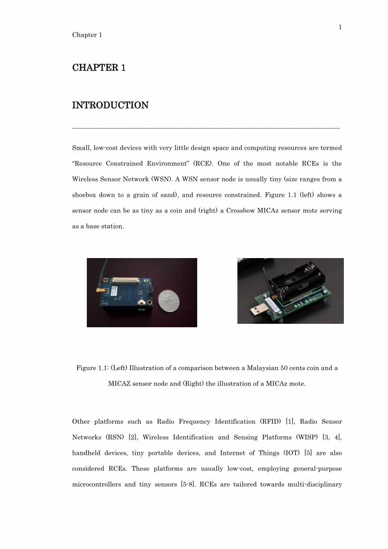
Small, low-cost devices with very little design space and computing resources are termed
“Resource Constrained Environment” (RCE). One of the most notable RCEs is the
Wireless Sensor Network (WSN). A WSN sensor node is usually tiny (size ranges from a
shoebox down to a grain of sand), and resource constrained. Figure 1.1 (left) shows a
sensor node can be as tiny as a coin and (right) a Crossbow MICAz sensor mote serving
as a base station.
Figure 1.1: (Left) Illustration of a comparison between a Malaysian 50 cents coin and a
MICAZ sensor node and (Right) the illustration of a MICAz mote.
Other platforms such as Radio Frequency Identification (RFID) [1], Radio Sensor
Networks (RSN) [2], Wireless Identification and Sensing Platforms (WISP) [3, 4],
handheld devices, tiny portable devices, and Internet of Things (IOT) [5] are also
considered RCEs. These platforms are usually low-cost, employing general-purpose
microcontrollers and tiny sensors [5-8]. RCEs are tailored towards multi-disciplinary

2
Chapter 1
applications such as real-time surveillance systems, environmental and health care
monitoring systems, asset tracking and even advanced military applications that deals
with various data such as general plaintexts, imagery and videos. RCE platforms that
are equiped with visual sensors such as the Wireless Visual Sensor Network (WVSN)
adopt Field Programmable Gate Array (FPGA) for the advantage in terms of flexibility
and field re-programmability [9]. Ultimately, the visual sensor field-reconfigurable RCE
[10-12] is the most popular and useful platform for the wide range of applications it
offers to the users [13-15].
Every RCE requires hardware that is tailored to a specific application to minimize cost,
power requirements and size and to maximize reliability as they are often left in the field
and not intended to be maintained for extended periods of time [16]. While typical RCEs
collect environmental data, visual sensor RCEs require more on-node processing such as
applying computer vision techniques and compression. For efficiency, availability and
cost reasons, FPGAs are typically used as the processing unit for the RCE node [12, 17,
18]. The change in the data type collected from scalar to visual data creates a security
and privacy issue as the data is transmitted over unsecured wireless channels. To
address this problem, cryptography can be used to encrypt the information before being
sent. While complex data processors and crypto-processors (CP) working side-by-side are
the best combination for robust and secured system, this may not be feasible in RCE
systems due to size, power and cost constraints. One of the main aims of this research is
to create a low-area, low-complexity CP that can be integrated into RCE devices with
FPGAs such as in visual RCEs. This is a challenge as each RCE hardware will have
varying amounts of un-utilized logic leading to the need for a design and implementation
of low-complexity, low-area crypto-processors for RCEs. [5, 6, 19-22].
A crypto-processor, is a processor that carries out cryptographic operations [23]. A
dedicated CP for RCE, constrained by RCE restrictions [24], has to provide sufficient
cryptographic functions and flexibility in terms of handling diverse RCE security
requirements [25, 26]. A CP uses hardware-accelerated cryptographic functions to

3
Chapter 1
provide and formulate security features and protocols such as double or multiple
encryption [27, 28], multi-cipher [29], support for cipher mode of operation [30], multi-
level security [31], key management [32], authentication [33], and digital signature are
preferable in facing multiple RCE security threats [31]. However, crypto-processors with
accelerated crypto-cores requires additional hardware [34]. The cost is greater when
multiple un-rolled ciphers cores are added to support multiple cryptographic functions
[35]. An alternative solution is to design a crypto-processor that utilizes the same crypto-
blocks for various ciphers without additional logic components, at a cost of cipher
program memory.
Low-complexity computer models are considered in the course of designing a low-area
crypto-processor. The Ultimate Reduced Instruction Set Computer (URISC) fits the
profile by having a low-complexity but yet completely functional computing architecture,
suitable for low-complexity applications. The prominent feature of URISC is that it uses
only a single instruction set. Through minimalistic modifications and adding resource-
justified application-specific crypto-components, low-area, low-complexity cryptographic
applications can be designed. Hence URISC-based modified minimalist reconfigurable
cryptographic processors for low-area, low complexity cryptographic applications in RCE
are proposed in this thesis.
While cryptographic solutions are widely used, certain primitives, schemes, and protocols
are applicable to visual sensor RCE due to the type of the data involved (video, image
and plaintext), the worth (value) of the data, the computation, resource overhead and
security requirements [5, 19, 21, 25, 36-38]. These factors will shape and determine the
type of crypto-processors designed and the choice of ciphers. Visual sensor RCE requires
visual processing techniques such as data compression to reduce the amount of data
transmitted [39]. Security can be introduce using techniques such as partial and
selective encryption [40-42], taking advantage of the characteristics of compressed data.
The combination of compression and selective encryption results to a robust system that
4
Chapter 1
decreases the amount of data to encrypt and transmit, allowing more memory to be use
for cipher programs.
This thesis presents low-area modified URISC reconfigurable processor architecture for
visual sensor RCE cryptographic applications. The proposed modified URISC enables
security in power and cost contrained RCE applications. A lower-area, low-complexity
cryptographic processor using the proposed modified URISC as cores, results to flexible
and versatile configurations, aiding the need for multiple security solutions. Lastly, the
proposed architecture is presented and integrated into a selective encryption system, to
emulate on-node encryption, using real world FPGA as a low-power and low-cost RCE
device.

5
Chapter 1
1.1. Problem Statement
RCEs operate under very restrictive conditions. Power and computation is always the main issue
while designing the application framework using these devices [43, 44]. In extreme cases, trade-
offs in security have to be made for a functional system and a longer operational lifespan [45]. On
top of that, RCE devices possess some form of communication ability for them to communicate
with nearby devices, forming a network of data. With existence of communication between
different devices, security risks increase. The risks are even higher when the payload data is
valuable to any party of interest. Hence security plays an important part when the system is
designed and the already scarce resources in the system [46].
RCE is broad by definition but the typical resource constrained design issues remain regardless
of the platforms it takes. Low-complexity, low-memory, low-area, and low-power are the critical
factors to be considered. And by extension, a smaller area utilized on the same reconfigurable
hardware will result in reduced power requirement [47, 48].
When designing for RCE systems, although often holistic, there are a few important design
issues to be addressed:
1) Limited or non-renewable on-board power.
2) Finite capacity of storage memory.
3) Small physical design space.
4) Limited communication bandwidth.
5) Limited computing power.
6) Low-upgradability.
In the context of a reconfigurable RCE, the points 1), 2) and 3) above implied that the amount of
logic and memory resources is limited. Within this context, the constrained resource or the
hardware costs taken into consideration when designing a cryptographic processor is the area
utilized and memory resources used within the reconfigurable hardware.
6
Chapter 1
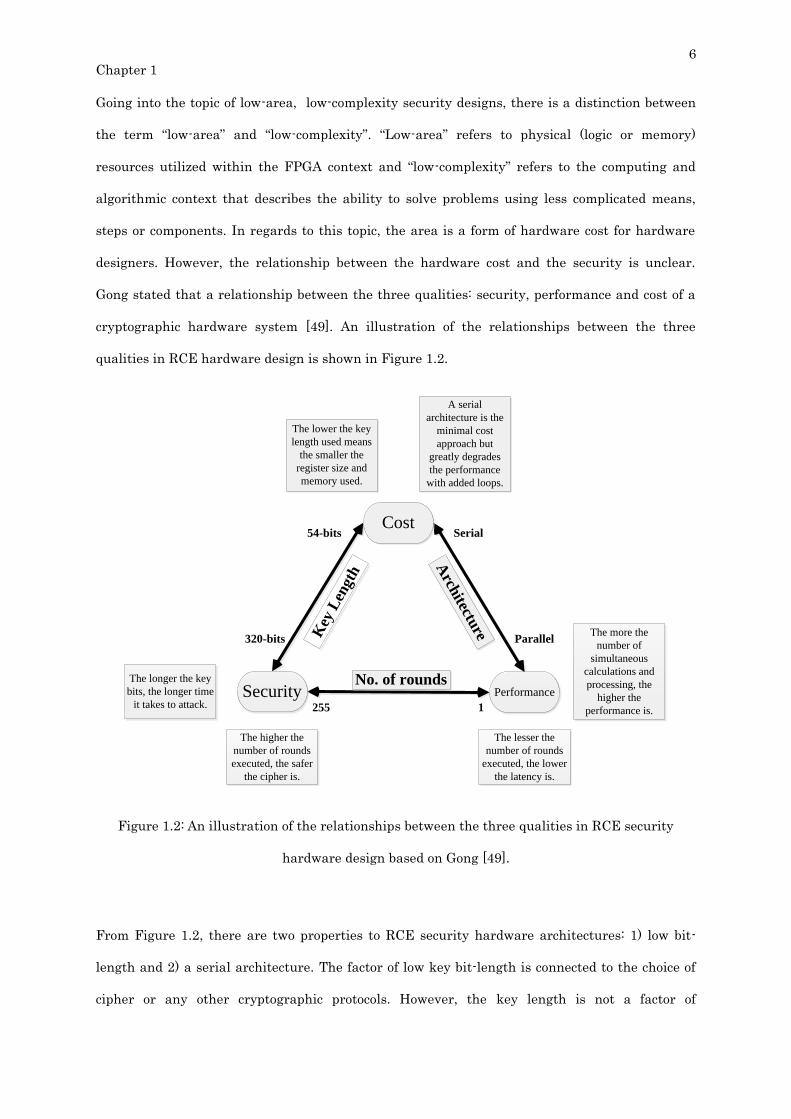
Going into the topic of low-area, low-complexity security designs, there is a distinction between
the term “low-area” and “low-complexity”. “Low-area” refers to physical (logic or memory)
resources utilized within the FPGA context and “low-complexity” refers to the computing and
algorithmic context that describes the ability to solve problems using less complicated means,
steps or components. In regards to this topic, the area is a form of hardware cost for hardware
designers. However, the relationship between the hardware cost and the security is unclear.
Gong stated that a relationship between the three qualities: security, performance and cost of a
cryptographic hardware system [49]. An illustration of the relationships between the three
qualities in RCE hardware design is shown in Figure 1.2.
Key
Len
gth
Arch
itecture
No. of rounds
Cost
Security Performance
The higher the
number of rounds
executed, the safer
the cipher is.
The lower the key
length used means
the smaller the
register size and
memory used.
The lesser the
number of rounds
executed, the lower
the latency is.
The more the
number of
simultaneous
calculations and
processing, the
higher the
performance is.
The longer the key
bits, the longer time
it takes to attack.
320-bits
54-bits Serial
Parallel
255 1
A serial
architecture is the
minimal cost
approach but
greatly degrades
the performance
with added loops.
Figure 1.2: An illustration of the relationships between the three qualities in RCE security
hardware design based on Gong [49].
From Figure 1.2, there are two properties to RCE security hardware architectures: 1) low bit-
length and 2) a serial architecture. The factor of low key bit-length is connected to the choice of
cipher or any other cryptographic protocols. However, the key length is not a factor of
7
Chapter 1
performance because the length of a key is attributed to cipher’s strength and mode of operations
chosen. The key length barely affects the performance and the effects only applies to asymmetric
ciphers [50, 51]. In short, the resource cost in relation to the cryptographic protocol is subject to
the protocol’s designer and the protocol’s specification, to a certain key-length in order for the
cipher to be consider secured [52].
On the other hand, a serial architecture suggests a sequential von-Neumann model. URISC
fulfills the requirement for a basic serial computing architecture because it is claimed to be the
simplest form of functional computer architecture [53, 54]. This serial computer with only a
single instruction set poses very obvious weaknesses in terms of complex functionality and high-
level operations. By using techniques like assembly code re-use, program-loops, instruction
sequencing, parameterization, self-modifying codes, and sub-routines [55, 56], the limitations of
URISC can be overcome. Initially, the URISC was proposed in [56] as an educational model to
better understand the concept of computer organization and there are other numerous
applications which can be found in [57-60]. But the simplicity of its fundamental building blocks
and data processing components are very attractive features to be explored for complicated
computing tasks. Hence URISC fulfills the requirement of a low-complexity, sequential
architecture without the need to design an architecture from scratch. The real problem is what
and how modifications can be done onto URISC fulfill the requirements of low-area, low-
complexity cryptographic applications. The URISC, like any other instruction set computer
architecture, has a fundamental data path and a memory unit. Alteration, addition and
customization of low-complexity cryptopgrahic components on URISC yields a custom-designed
architecture to suit any target application.
RCE devices vary in terms of form factor and hardware. To allow adequate level of security,
complex security algorithms and protocols are considered. Visual sensor RCE has the broader
context in terms of applications, from simple data relaying to complex video surveilance. Visual
RCEs can be used as the target application, which inherits the model of common security and
privacy problems within general RCEs. By using visual sensor RCE as point of reference to the
generalization of RCE cryptographic problems, the six known security goals are [20, 61]:
8
Chapter 1
1) Confidentiality: protecting secret information from unauthorized entities.
2) Integrity: ensuring message has not been altered by malicious parties.
3) Data Origin Authentication: authenticating the source of message.
4) Entity Authentication: authenticating the user, node and sink is indeed whom it claims
to be.
5) Access control: restricting access of resource to privileged parties.
6) Availability: ensuring desired services available when required.
Goal 1), 2), 3), and 4) can be fulfilled using a combination of cryptographic algorithms, key
management, and authentication, which are considered as cryptographic solutions. Goal 5) and 6)
can be solved using attack detection, prevention and routing techniques [20, 61]. One common
form of cryptographic solution is the direct use of cryptographic primitives, which are referred to
as ‘ciphers’. Ciphers are generally divided into two types: symmetric and asymmetric. For low-
area, low-complexity applications, symmetric ciphers are preferred due to their nature of being
hardware implementation-friendly [61, 62]. Law et al [19] concluded that the Skipjack cipher [63]
is the best lightweight cipher in terms of code memory, data memory, encryption efficiency and
key setup efficiency and it is also used in Tinysec for WSN RCEs [64]. However, the Skipjack
cipher is not the best and strongest cipher but would suffice for a lightweight security application
[19].
On the contrary, Rijndael [65] also known as the Advanced Encryption Standard (AES) [66] is
one of the most popular, strongest and resilient cipher to most known attacks. On top of that, [67]
concluded that an AES hardware out-performs any software implementation, which further
validates the cipher choice. However, the AES is known to be resource demanding due to the
complex encryption operations and the non-linear component named the S-box [68-71].
Minimizing the S-box [70-72] is one method towards low-area designs.
Futhermore, AES and Skipjack are just two out of the long list of ciphers available to choose from
depending on applications and level of security required [73]. In a real world scenario where
RCEs are deployed into a hostile environment, secure frameworks [74, 75] utilizes crypto-
processors to ensure critical data do not fall into the wrong hands [76]. Dedicated CP with
9
Chapter 1
multiple cryptographic functions and primitives provides variable degree of security for RCE
secure frameworks. To achieve this, multiple ciphers accelerators within a scalable CP are
introduced [77, 78]. Multi-cipher and multi-mode systems on the hardware level offer multiple
cipher algorithms concurrently in a communication session [77, 78], variation of security strength
and application [29]. These primitives can be replaced when they are outdated or obselete, via
techniques such as partial or dynamic reconfiguration [9] using FPGA reconfigurable hardware.
Nonetheless, having multiple cipher accelerators will logically require additional memory and
logic resources which is already scarce in RCE. A low-complexity multi-cipher [29, 35, 77]
architecture would be the solution to accommodate multiple cryptographic primitives. By re-
using the same crypto-blocks, multi-ciphers exists with only program memory costs rather than
using both the logic and memory resources. Hence multiple cipher switching is made available
and by extension reducing the resources used compared to having the cipher cores in separate
entities.
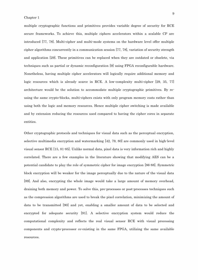
Other cryptographic protocols and techniques for visual data such as the perceptual encryption,
selective multimedia encryption and watermarking [42, 79, 80] are commonly used in high-level
visual sensor RCE [15, 81-85]. Unlike normal data, pixel data is very information rich and highly
correlated. There are a few examples in the literature showing that modifying AES can be a
potential candidate to play the role of symmetric cipher for image encryption [86-88]. Symmetric
block encryption will be weaker for the image perceptually due to the nature of the visual data
[89]. And also, encrypting the whole image would take a large amount of memory overhead,
draining both memory and power. To solve this, pre-processes or post-processes techniques such
as the compression algorithms are used to break the pixel correlation, minimizing the amount of
data to be transmitted [90] and yet, enabling a smaller amount of data to be selected and
encrypted for adequate security [91]. A selective encryption system would reduce the
computational complexity and reflects the real visual sensor RCE with visual processing
components and crypto-processor co-existing in the same FPGA, utilizing the same available
resources.
10
Chapter 1
To form a cryptographic solution, algorithmic understanding and translation to hardware form is
key. However, the vast option of cryptographic techniques and goals leads to the problem of
cryptographic versatility and selection. A well-designed cryptographic processor for RCE has to
possess the necessary security functions and primitives, making it adequate for formulating
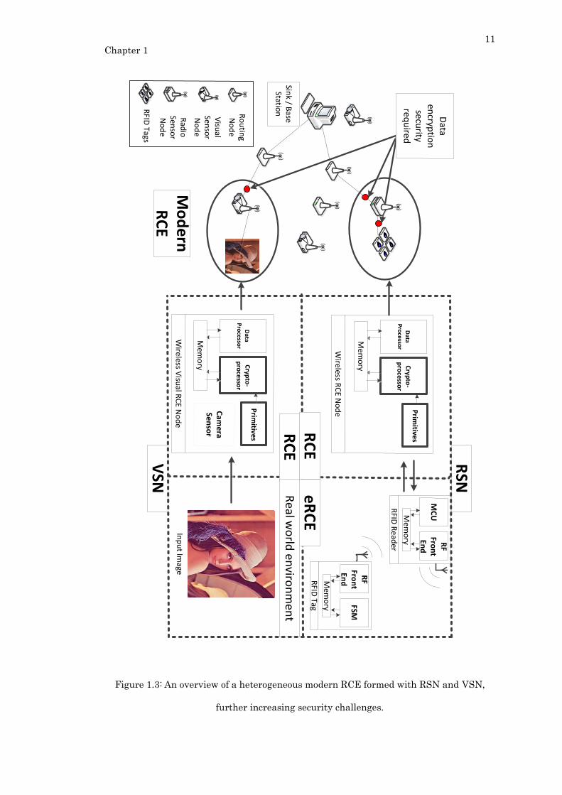
secure protocols. Using modified URISC as a fundamental model, and the generalized RCE
security goals, custom-designed processor are presented for low-area, low-complexity for
cryptographic applications suitable for RCEs. Figure 1.3 illustrates the ubiquitous and pervasive
nature of RCE devices, forming unique RCE networks. RSN is a network formed by RCE devices
integrating with RFID (termed eRCE) and VSN RCE is formed by devices equipped with camera
sensors. Larger heterogenous modern RCEs can be collectively formed by these types of networks
and devices thus, leading to various security challenges that requires a flexible crypto-processor.
The red dots depicted in Figure 1.3 shows the points where data security is required for a robust
and secured RCE.
1.2. Research Aims and Objectives
The aim of the research presented in this thesis is to design and develop low-area, low-complexity
security architectures with modified URISC, using FPGA. The main objectives of this research
are as follow:
1) Modifying the URISC low-complexity processor for RCE cryptographic application.
2) Develop a low-area, lightweight cipher processor architecture suitable for lightweight
specific applications using Skipjack cipher.
3) Develop a low-area, modern cipher processor architecture for modern cryptographic
application using AES cipher
4) Develop a low-complexity architecture that allows multiple ciphers that will work
towards providing additional cryptographic primitives in a single architecture.
5) Design and develop a selective encryption system that reflects real-world practicality,
employing one of the proposed architecture and an image compression technique to form
a joint encryption system.
11
Chapter 1
Wireless R
CE N
od
e
RF
Fron
t En
dM
CUM
emo
ry
RFID
Read
er
RF
Fron
t En
dFSM
Mem
ory
RFID
Tag
Cryp
to-
pro
cesso
rD
ata P
roce
ssor
Mem
ory
Wireless V
isual R
CE N
od
e
Cam
era
Sen
sor
Inp
ut Im
age
RC
Ee
RC
E
Cryp
to-
pro
cesso
rD
ata P
roce
ssor
Mem
ory
Prim
itives
Prim
itives
RC
ER
eal wo
rld en
viron
men
t
Mo
de
rn
RC
E
RSN
VSN
Data
encryp
tion
secu
rity req
uired
Ro
utin
g N
od
e
Visu
al Sen
sor
No
de
RFID
Tags
Rad
io
Senso
r N
od
e
Sink / B
ase Statio
n
Figure 1.3: An overview of a heterogeneous modern RCE formed with RSN and VSN,
further increasing security challenges.
12
Chapter 1
1.3. Author’s Contributions
1.3.1. Low-complexity Two Instruction Set Computer using Skipjack
(TISC Skipjack) for Lightweight Cryptographic Implementation
For the area of lightweight security, the design of a low-complexity architecture using
only two instruction sets, capable of completely execute full 32 rounds of Skipjack cipher
is proposed. Skipjack has been introduced as the most suitable candidate for lightweight
cipher.. selection in the area of WSN RCE [19]. The proposed architecture (found in
Chapter 3) is extremely compact and is designed by modifying URISC to accommodate
an additional ALU, which is the XOR.
1.3.2. Low-complexity Compact Instruction Set Architecture using
Advanced Encryption Standard (CISA AES) for Modern
Cryptographic Implementation
For the area of modern security solutions, the design of a low-complexity architecture
using only four instruction sets, capable of completely execute full ten rounds of AES
cipher is proposed. The proposed compact architecture is designed by modifying the TISC
Skipjack architecture (found in Chapter 3) due to the overlapping components used for
both architectures. The new architecture (found in Chapter 4) accommodates two
additional ALUs, XTIME and S-BOX. This newly modified URISC results in a four
instruction set, low-complexity, low logic area, compact architecture specifically for AES.
1.3.3. Bi-directional S-BOX gate count improvement
The AES S-BOX is a large combinational circuit and has always been one of the most
resource demanding component for AES hardware implementation [92, 93].
13
Chapter 1
Improvement on the current bi-directional S-box suggests the application of linear
matrix mapping optimization on the inverse affine transformation block. The improved
configuration of a forward direction S-box together with a minimized inverse affine
transformation block (found in Chapter 4) shows results to a smaller, low-complexity bi-
direction S-box, in which would be reflected in the hardware implementation results.
1.3.4. Multi-Cipher Architecture (MCA) featuring Arithmetic Logic Unit
(ALU) Sharing
The MCA uses AES and Skipjack ciphers in single processor. The previous work (1.3.1,
1.3.2) was extended to find low-complexity multi-cipher configurations, a single modified
URISC is used to process two different ciphers by sharing the same set of ALUs. This
design opens up a new area to RCE multi-cipher systems in sharing the same processing
blocks. This would provide solutions to having multiple cryptographic primitives at the
costs of program code memory, while retaining the same amount of logic resources used.
1.3.5. Real-world Hardware Implementation of Selective Encryption
Architecture (SEA)
A real-world design and hardware implementation of a SEA for joint security and
compression application is realized. A complete working system is presented in this
thesis demonstrating the functionality and feasibility of the proposed CISA AES. The
proposed design integrates an MIPS-SPIHT compression module with a CISA AES
module for real-world selective encryption application.
14
Chapter 1
1.4. Thesis Organization
The thesis structure is as follows. Chapter 2 provides the literature review and
background knowledge of related works in the area of RCEs, symmetric cipher primitives,
multi-ciphers and selective encryption. Chapter 3 presents a low-area low-complexity
FPGA TISC for lightweight cipher using Skipjack using a modified URISC. Chapter 4
presents a low-complexity FPGA CISA, customized specifically for AES, with minimized
S-box in terms of gate count. Chapter 5 describes a low-complexity multi-cipher
architecture symmetric ciphers switching. Chapter 6 presents a low-complexity selective
encryption architecture as a practical example of the real-world application of the CISA
AES architecture. Lastly, Chapter 7 presents the conclusion of this thesis with potential
future work and directions discussed.
15
Chapter 2
CHAPTER 2
LITERATURE REVIEW
__________________________________________________________________________________
2.1. Resource Constrained Environments (RCE)
RCEs are generally referred to as small hardware systems or devices with very low
amount of resources in terms of power supply, memory, communication bandwidth, and
storage memory1. There are currently four known resource constrained environments
identified:
1) Wireless Sensor Network (WSN) [19, 25, 94, 95]
2) Radio Frequency Identification (RFID) [2, 96-98]
3) Wireless Identification and Sensing Platform (WISP) [3, 4]
4) Internet of Things (IOT) [5, 99]
All the generalized RCEs share similar problems when it comes to hardware design due
to the scarce resources on the RCE devices. However, there are differences between
environments in terms of hardware form factors, specifications, communication
standards and target applications. To understand the need for low-complexity, low-area
cryptographic processors, each of the four RCEs are briefly discussed.
2.1.1. Wireless Sensor Networks (WSNs)
A wireless sensor network is usually made up of tiny sensors that are programmed to
communicate via wireless medium [100]. The limitation of their physical size results in
sensor motes that usually have limited amount of on-board resources such as energy,
1 Review of all 4 environments published in “J. H. Kong, L.-M. Ang, and K. P. Seng, "A
comprehensive survey of modern symmetric cryptographic solutions for resource constrained
environments," Journal of Network and Computer Applications, vol. 49, pp. 15-50, 2015”.
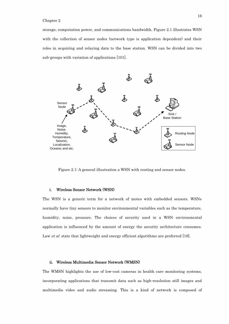
16
Chapter 2
storage, computation power, and communications bandwidth. Figure 2.1 illustrates WSN
with the collection of sensor nodes (network type is application dependent) and their
roles in acquiring and relaying data to the base station. WSN can be divided into two
sub-groups with variation of applications [101].
Routing Node
Sensor Node
Sink /
Base Station
Sensor
Node
Image,
Noise,
Humidity,
Temperature,
Seismic,
Localization,
Oceanic and etc.
Figure 2.1: A general illustration a WSN with routing and sensor nodes.
i. Wireless Sensor Network (WSN)
The WSN is a generic term for a network of motes with embedded sensors. WSNs
normally have tiny sensors to monitor environmental variables such as the temperature,
humidity, noise, pressure. The choices of security used in a WSN environmental
application is influenced by the amount of energy the security architecture consumes.
Law et al state that lightweight and energy efficient algorithms are preferred [19].
ii. Wireless Multimedia Sensor Network (WMSN)
The WMSN highlights the use of low-cost cameras in health care monitoring systems,
incorporating applications that transmit data such as high-resolution still images and
multimedia video and audio streaming. This is a kind of network is composed of

17
Chapter 2
embedded audio and visual collection modules that require the balancing of the energy
costs, application purposes, and security strength considerations [102].
iii. Wireless Visual Sensor Network (WVSN)
This type of network features the use of visual sensors or low-cost cameras for
environmental surveillance purposes. The crucial area of consideration for WVSN is low
latency of communication and image processing modules. The real-time systems are
extremely resource constrained, making designers find extreme measures without
compromising significant costs [13].
According to Roman et al [6], microcontrollers are used in the WSN because of their cost-
effectiveness. Microcontrollers are grouped into weak, normal and heavy-duty for their
computing capabilities, clock speed, and RAM size. Figure 2.2 illustrates an overview of
the architecture within a WSN node, including the connections of the microcontroller to
other input/output components. Roman et al questioned the suitability of some of the
symmetric cryptographic primitives for some low-end microcontrollers. The
cryptographic primitive in question are the AES cipher and Twofish cipher, which both
are known to be optimized for 32-bit processors. However, some of the operations can be
done using native 8-bit registers [6]. Heavy-duty controllers, such as the PXA271 or the
ARM920T with a word size of 32-bits, are compatible with these ciphers. The Skipjack
cipher fits perfectly into the MSP430 family because the operations and the key schedule
use 16-bit words [103]. The instruction memory and the RAM memory of the RCE have
to suffice for the storage of: program code, private key, intermediate values, and other
temporary data. This shows that choosing a cipher to match a microcontroller’s resources
is an important consideration.

18
Chapter 2
Figure 2.2: An illustration of the generic architecture within a WSN node (image
extracted from [6]).
Johnson et al reviewed the most recent specifications of sensor motes [104].
Table 2.1 shows the hardware specifications of known motes. Mark Hempstead [95]
provided a detailed analysis of hardware systems for sensor nodes, focusing on the
architectural level of the processors used. Hempstead concluded that it would be difficult
to judge the programmability, energy efficiency, and performance fairly without running
the same benchmarking application on all these different systems. Hempstead stated
that the intelligent combination of: circuit techniques, hardware architecture and
application support can yield ultra-low power systems.
Table 2.2 shows a summarized version of the table presented in [95].
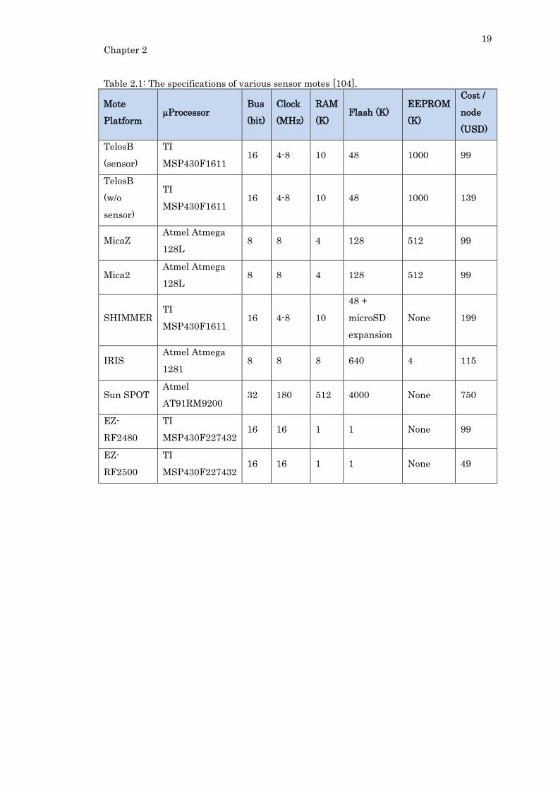
19
Chapter 2
Table 2.1: The specifications of various sensor motes [104].
Mote
Platform µProcessor
Bus
(bit)
Clock
(MHz)
RAM
(K) Flash (K)
EEPROM
(K)
Cost /
node
(USD)
TelosB
(sensor)
TI
MSP430F1611 16 4-8 10 48 1000 99
TelosB
(w/o
sensor)
TI
MSP430F1611 16 4-8 10 48 1000 139
MicaZ Atmel Atmega
128L 8 8 4 128 512 99
Mica2 Atmel Atmega
128L 8 8 4 128 512 99
SHIMMER TI
MSP430F1611 16 4-8 10
48 +
microSD
expansion
None 199
IRIS Atmel Atmega
1281 8 8 8 640 4 115
Sun SPOT Atmel
AT91RM9200 32 180 512 4000 None 750
EZ-
RF2480
TI
MSP430F227432 16 16 1 1 None 99
EZ-
RF2500
TI
MSP430F227432 16 16 1 1 None 49
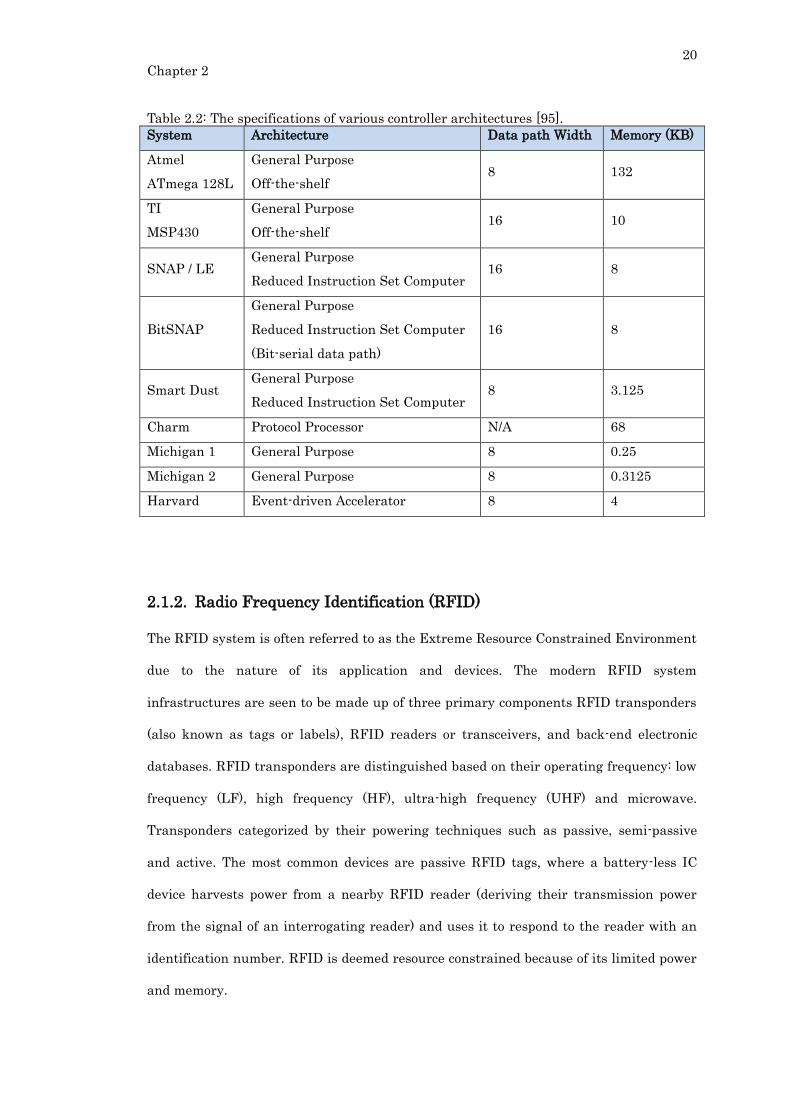
20
Chapter 2
Table 2.2: The specifications of various controller architectures [95].
System Architecture Data path Width Memory (KB)
Atmel
ATmega 128L
General Purpose
Off-the-shelf 8 132
TI
MSP430
General Purpose
Off-the-shelf 16 10
SNAP / LE General Purpose
Reduced Instruction Set Computer 16 8
BitSNAP
General Purpose
Reduced Instruction Set Computer
(Bit-serial data path)
16 8
Smart Dust General Purpose
Reduced Instruction Set Computer 8 3.125
Charm Protocol Processor N/A 68
Michigan 1 General Purpose 8 0.25
Michigan 2 General Purpose 8 0.3125
Harvard Event-driven Accelerator 8 4
2.1.2. Radio Frequency Identification (RFID)
The RFID system is often referred to as the Extreme Resource Constrained Environment
due to the nature of its application and devices. The modern RFID system
infrastructures are seen to be made up of three primary components RFID transponders
(also known as tags or labels), RFID readers or transceivers, and back-end electronic
databases. RFID transponders are distinguished based on their operating frequency: low
frequency (LF), high frequency (HF), ultra-high frequency (UHF) and microwave.
Transponders categorized by their powering techniques such as passive, semi-passive
and active. The most common devices are passive RFID tags, where a battery-less IC
device harvests power from a nearby RFID reader (deriving their transmission power
from the signal of an interrogating reader) and uses it to respond to the reader with an
identification number. RFID is deemed resource constrained because of its limited power
and memory.
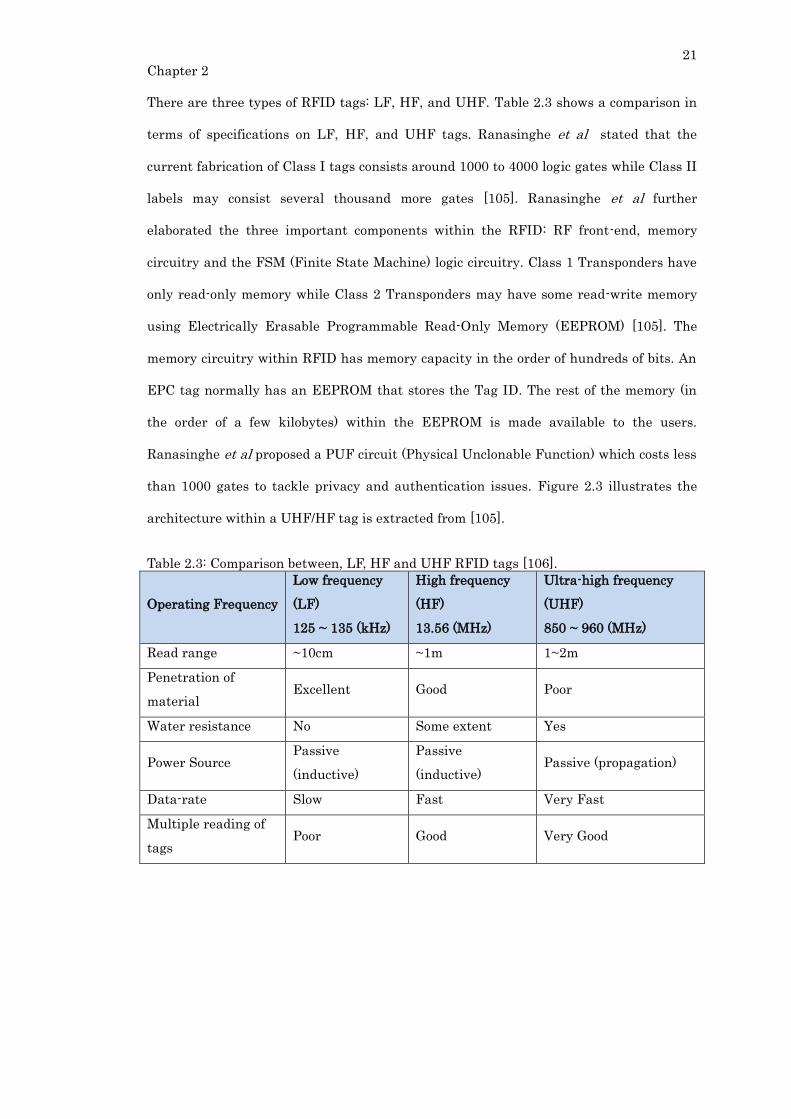
21
Chapter 2
There are three types of RFID tags: LF, HF, and UHF. Table 2.3 shows a comparison in
terms of specifications on LF, HF, and UHF tags. Ranasinghe et al stated that the
current fabrication of Class I tags consists around 1000 to 4000 logic gates while Class II
labels may consist several thousand more gates [105]. Ranasinghe et al further
elaborated the three important components within the RFID: RF front-end, memory
circuitry and the FSM (Finite State Machine) logic circuitry. Class 1 Transponders have
only read-only memory while Class 2 Transponders may have some read-write memory
using Electrically Erasable Programmable Read-Only Memory (EEPROM) [105]. The
memory circuitry within RFID has memory capacity in the order of hundreds of bits. An
EPC tag normally has an EEPROM that stores the Tag ID. The rest of the memory (in
the order of a few kilobytes) within the EEPROM is made available to the users.
Ranasinghe et al proposed a PUF circuit (Physical Unclonable Function) which costs less
than 1000 gates to tackle privacy and authentication issues. Figure 2.3 illustrates the
architecture within a UHF/HF tag is extracted from [105].
Table 2.3: Comparison between, LF, HF and UHF RFID tags [106].
Operating Frequency
Low frequency
(LF)
125 ~ 135 (kHz)
High frequency
(HF)
13.56 (MHz)
Ultra-high frequency
(UHF)
850 ~ 960 (MHz)
Read range ~10cm ~1m 1~2m
Penetration of
material Excellent Good Poor
Water resistance No Some extent Yes
Power Source Passive
(inductive)
Passive
(inductive) Passive (propagation)
Data-rate Slow Fast Very Fast
Multiple reading of
tags Poor Good Very Good
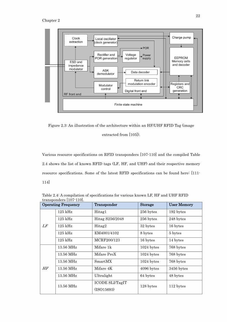
22
Chapter 2
Figure 2.3: An illustration of the architecture within an HF/UHF RFID Tag (image
extracted from [105]).
Various resource specifications on RFID transponders [107-110] and the compiled Table
2.4 shows the list of known RFID tags (LF, HF, and UHF) and their respective memory
resource specifications. Some of the latest RFID specifications can be found here: [111-
114]
Table 2.4: A compilation of specifications for various known LF, HF and UHF RFID
transponders [107-110].
Operating Frequency Transponder Storage User Memory
LF
125 kHz Hitag1 256 bytes 192 bytes
125 kHz Hitag S256/2048 256 bytes 248 bytes
125 kHz Hitag2 32 bytes 16 bytes
125 kHz EM4001/4102 8 bytes 5 bytes
125 kHz MCRF200/123 16 bytes 14 bytes
HF
13.56 MHz Mifare 1k 1024 bytes 768 bytes
13.56 MHz Mifare ProX 1024 bytes 768 bytes
13.56 MHz SmartMX 1024 bytes 768 bytes
13.56 MHz Mifare 4K 4096 bytes 3456 bytes
13.56 MHz Ultralight 64 bytes 48 bytes
13.56 MHz ICODE SLI/TagIT
(ISO15693) 128 bytes 112 bytes

23
Chapter 2
Operating Frequency Transponder Storage User Memory
13.56 MHz Mu-chip 128 bits -
UHF
902 – 928 MHz Alien I2
(ALL-9250) 64 bits -
902 – 928 MHz Alien M
(ALL-9254) 64 bits -
902 – 928 MHz Alien Squiggle
(ALL-9238) 64 bits -
860 – 960 MHz IT36 Low Profile
Durable Asset Tag
TID = 64 bits
EPC = 128
bits
512 bits
902 – 928 MHz IT75 Low Profile
Durable Asset Tag
TID = 64 bits
EPC = 128
bits
512 bits
865 – 868 MHz IT76 Low Profile
Durable Asset Tag
TID = 64 bits
EPC = 128
bits
512 bits
860 – 960 MHz
IT67 Enterprise
Lateral Transmitting
(LT) Tag
TID = 64 bits
EPC = 240
bits
512 bits
860 – 960 MHz IT65 Large Rigid Tag,
Gen2
TID = 32 bits
EPC = 96 bits 0 bits
869 / 915 MHz Tire Tag Insert - -
915 MHz Container Tag - -
902 – 928 MHz Matrics / Symbol
Dual Dipole
TID = 112
bits
EPC = 128
bits
-
902 – 928 MHz Matrics / Symbol
Single Dipole
TID = 112
bits
EPC = 128
bits
-
An enhanced version of RFID device called the Computational RFID (CRFID) has
emerged in the recent years [115], bridging the gap between WSN and RFID with added
sensing and computation abilities.
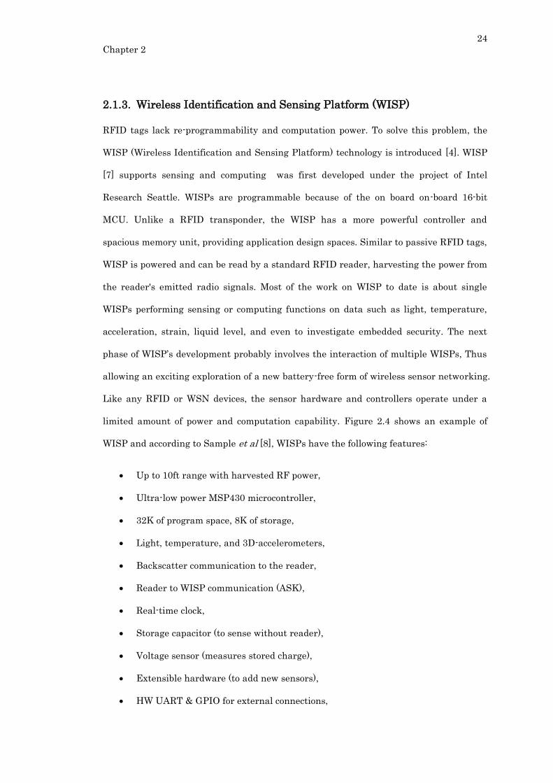
24
Chapter 2
2.1.3. Wireless Identification and Sensing Platform (WISP)
RFID tags lack re-programmability and computation power. To solve this problem, the
WISP (Wireless Identification and Sensing Platform) technology is introduced [4]. WISP
[7] supports sensing and computing was first developed under the project of Intel
Research Seattle. WISPs are programmable because of the on board on-board 16-bit
MCU. Unlike a RFID transponder, the WISP has a more powerful controller and
spacious memory unit, providing application design spaces. Similar to passive RFID tags,
WISP is powered and can be read by a standard RFID reader, harvesting the power from
the reader's emitted radio signals. Most of the work on WISP to date is about single
WISPs performing sensing or computing functions on data such as light, temperature,
acceleration, strain, liquid level, and even to investigate embedded security. The next
phase of WISP’s development probably involves the interaction of multiple WISPs, Thus
allowing an exciting exploration of a new battery-free form of wireless sensor networking.
Like any RFID or WSN devices, the sensor hardware and controllers operate under a
limited amount of power and computation capability. Figure 2.4 shows an example of
WISP and according to Sample et al [8], WISPs have the following features:
Up to 10ft range with harvested RF power,
Ultra-low power MSP430 microcontroller,
32K of program space, 8K of storage,
Light, temperature, and 3D-accelerometers,
Backscatter communication to the reader,
Reader to WISP communication (ASK),
Real-time clock,
Storage capacitor (to sense without reader),
Voltage sensor (measures stored charge),
Extensible hardware (to add new sensors),
HW UART & GPIO for external connections,

25
Chapter 2
Works with select EPC Class 1 Gen 2 readers,
WISP software to sense and upload data,
Reader application to drive WISP,
Industry standard development tools,
Access to hardware design and source code.
Figure 2.4: An illustration of WISP compared to a coin (Image extracted from [7]).
WISPs are programmable because of the on-board 16-bit MCU. Unlike a RFID
transponder, the WISP has a more powerful controller and larger memory unit,
providing application design spaces. Currently, there are three versions of WISP [4, 116]
shown in Table 2.5.
Table 2.5: A table stating WISPs’ version and their current state of development.
WISP Name MCU Status
WISP 4.1DL (Blue) MSP-430F-2132 Ramping Production
WISP 4.0DL (Purple) MSP-430F-2274 Deprecated
WISP 3.0 MSP-430F-2272 -
WISP G2.0 (Red) MSP-430F-2012 Limited use
The most recent development is the WISP 5.0 but the information released is limited.
The price for WISP devices is also currently unknown as the project is open to academic
collaborators and the WISPs are only given if the project proposal is accepted. The WISP
proposal is still very recent and the publications and literatures related to WISP are
limited.
26
Chapter 2
Sample et al [8] has written a complete description of the WISP, breaking down the
WISP with detailed explanations from the analog front-end, the modulation and
demodulation, the digital section and power conditioning, packet coding and decoding to
the power requirements and duty cycle. Figure 2.5 shows an illustration of the hardware
architecture and components within the WISP.
Figure 2.5: An illustration of the WISP platform and its components [7, 8].
2.1.4. Internet of Things (IoT)
IoT [117] refers to the interconnectivity of embedded computers. IOT also extends its
definition of the connectivity between devices and computers beyond the traditional
machine-to-machine communication, offering advanced services, systems and
functionality. IOT devices are mostly embedded computing systems that have the nature
of low-power radios and low-computing power. Applications that researchers have
identified for the IOT includes: environmental monitoring, energy management,
industrial and asset management, home automation, healthcare monitoring systems, etc.
However, integration with the Internet implies that the IoT devices will have an IP
address as a unique identifier which inherits the security threats of a generic computer.
This connection of physical devices to the Internet allows the control of the devices
remotely, very similar to a WSN. IoT building blocks are generally termed Smart Objects
[117] are also identified as embedded systems connected to the Internet. Current IoT
market examples include smart thermostat systems, home electrical appliances that use

27
Chapter 2
Wi-Fi for remote monitoring, smart home systems, and any systems that generally
connected to other devices or systems via wireless protocols such as 3G, Wi-Fi, Bluetooth
and Near Field Communication (NFC).
Hardware specification and form factors of IoT smart devices vary but generally has the
following characteristics:
1) Six known forms: Tabs, Boards, Pads, Dust, Skin, and Clay [118, 119].
2) Commonly act as personalized smart mobile devices.
3) Have ubiquitous computing properties, similar to Sensor Networks.
2.1.5. Radio Sensor Network (RSN, Integration of RFID and WSN)
In general, WSN is usually used in an environment for sensing and monitoring
geographical, chemical, visual and even physical environment through various sources
such as geo-thermal, sound waves or even image. As for the RFID environment, any
object 'tagged' with an RFID tag is track-able and sense-able in digital form. By
deploying both tags and sensors, smart nodes are able to make use of the RFIDs for
intelligent monitoring for unusual events. Zhang et al [120] stated that the integration
of these two promising technologies would bring extended capabilities, scalability, and
portability as well as reduced unnecessary costs.
Lei et al and Xin et al suggest that the new integrated system will consist of three
classes of devices. The first class is that of wireless devices known as smart stations,
containing RF readers, network connectivity and an MCU and its primary task is to
monitor the tags. The second and third class devices are the tags and sensor nodes [98,
121]. Lei et al and Xin et al also presents several modes of application such as the smart
warehouse for asset theft detection, and another example is the smart forklift for
efficient asset storing. Besides the applications, practically there is a design for the
smart node proposed by Mason et al [2]. Mason et al presented a design using a Mica2
mote, interfaced with a TTL converter to allow communication to RF reader, and also
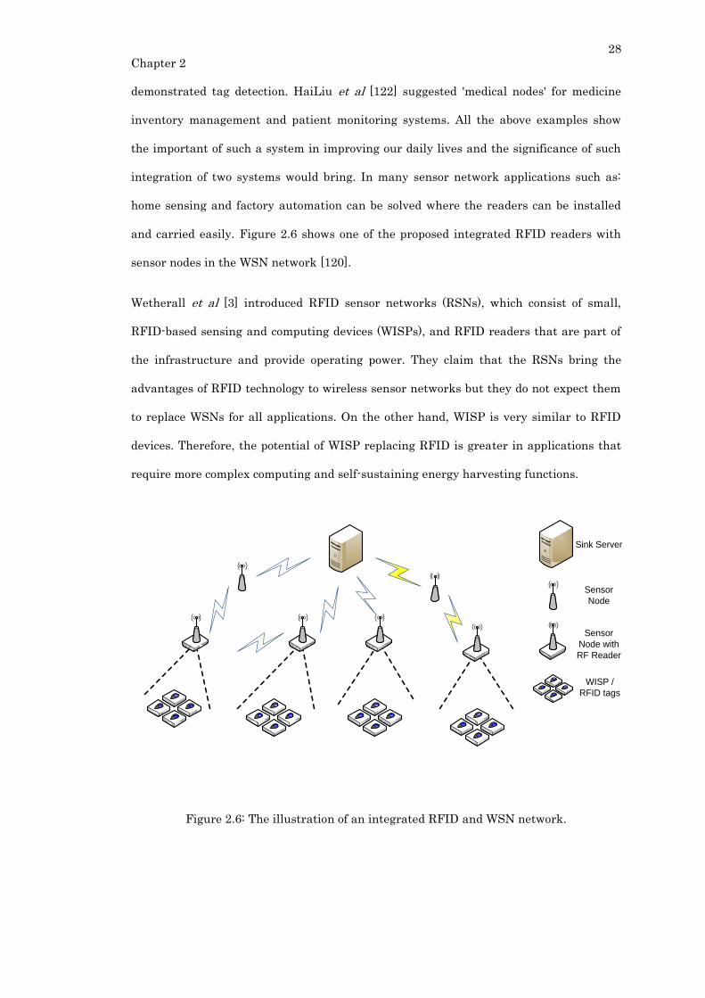
28
Chapter 2
demonstrated tag detection. HaiLiu et al [122] suggested 'medical nodes' for medicine
inventory management and patient monitoring systems. All the above examples show
the important of such a system in improving our daily lives and the significance of such
integration of two systems would bring. In many sensor network applications such as:
home sensing and factory automation can be solved where the readers can be installed
and carried easily. Figure 2.6 shows one of the proposed integrated RFID readers with
sensor nodes in the WSN network [120].
Wetherall et al [3] introduced RFID sensor networks (RSNs), which consist of small,
RFID-based sensing and computing devices (WISPs), and RFID readers that are part of
the infrastructure and provide operating power. They claim that the RSNs bring the
advantages of RFID technology to wireless sensor networks but they do not expect them
to replace WSNs for all applications. On the other hand, WISP is very similar to RFID
devices. Therefore, the potential of WISP replacing RFID is greater in applications that
require more complex computing and self-sustaining energy harvesting functions.
Sink Server
Sensor
Node
Sensor
Node with
RF Reader
WISP /
RFID tags
Figure 2.6: The illustration of an integrated RFID and WSN network.
29
Chapter 2
2.1.6. Distinction between RCE and eRCE
Section 2.1.1 to Section 2.1.5 showed that there are two classes of RCE: the typical RCEs
and the Extreme Resource Constrained Environment (eRCE or XRCE). Typical RCEs are
systems designed for complex applications and further defined by the sensory hardware
utilized. A typical example of visual sensor RCEs is the WVSN. eRCEs, such as RFID
tags, do not possess sensors [123].
Every RCE requires hardware that is tailored to a specific application to minimize cost,
power requirements and size and to maximize reliability because RCE devices are often
left in the field and not intended to be maintained for extended periods of time [16]. For
WSN and WISP RCEs, general purpose or RISC-like architecture is used as the
processing unit. Extreme RCEs such as the RFID UHF / HF transponder, application-
specific logic circuits is used to execute read-write commands. While typical RCEs collect
environmental data, visual sensor RCEs require more on-node processing such as
applying computer vision techniques and compression [124]. For efficiency, availability
and cost reasons, FPGAs are typically used as the processing unit for the visual sensor
RCE nodes [12, 17, 18].
The hardware property of RCE and eRCE affects the types of data processing algorithms
used. eRCE is extremely constrained compared to RCE. The extreme constrained nature
of eRCE led to the introduction and the adoption of lightweight algorithms [125, 126].
Many authors suggest that full cryptographic primitives (public key and private key) can
be used in RCE [127-131], the conservative estimation is that both RCE and eRCE will
employ algorithms that suit their resource budget. Thus, the algorithms used by both
systems will vary. Lightweight algorithms are more popular for eRCEs [49, 125, 132,
133]. The nature of both RCE and eRCE suggests that RCE has the slight flexiblity in
terms of utilizing modern cryptographic primitives. In contrast, the eRCE has a very
limited cipher-pool2 to choose from.
2 The findings of the cipher-pool is published in: Kong Jia Hao, Ang Li Minn, Seng Kah Phooi, “A
Comprehensive Survey of Modern Cryptographic Solutions for Resource Constrained

30
Chapter 2
2.1.7. IoT and RSN – Implications for Security
IoT RCE systems are becoming more prevalent and the devices within the network
ranges from small sensors to large televisions [5]. Like any other RCEs, IoT has the
underlying problem of a large spectrum of security problems and constrained resources
[125]. The options for security are public key or private key encryption but resource
required for public key primitives is much greater than the private key primitives [125].
Similar issues are found in other RCEs [128, 129]. Demand for key management using
private key cryptography [134, 135] is on the rise as an alternative to the Public Key
Cryptography. Key management protocols in IoT RCE are in high demand, leading to the
search for ‘lightweight’ public key primitives.
RSN [136] is a new type of network that incorperates both the RCE and eRCE [121].
Problem arises when secured data communication between RCE and eRCE has to be
established. Difference in security protocol, device manufacturer, and hardware
properties lead to the difference in cryptographic primitives employed. Encrypted data
from eRCE cannot be authenticated or decrypted unless both parties uses the same
protocol and the same key. A multi-cipher [78] crypto-system is able to solve the
disparity of cryptographic primitives by adopting the primitives used by the eRCE
counterpart. Key-predistribution with pair-wise keys [137] is able to solve the keying
issue. Alternatively, a pair of session key generated from a master key [138] can also be
used with the assumption that the RCE nodes only has to keep a single session key for a
single eRCE device connected. However, the number of session keys will grow at the rate
of N − 1 keys (N is the number of neighboring devices) and thus consuming memory
resources to store the large amount of keys [139].
Environments”, Journal of Network and Computer Applications, Vol. 49, No. 0, pp 15-50,
Elsevier 2014.

31
Chapter 2
2.2. Security in Visual Sensor RCE
Visual Sensor RCE security is a significant concern because the memory and
computational resources, required to store keys and run encryption programs, are
additional to the primary application.
There are two identified challenges regarding RCE security designs [5, 140]:
1) What are the security requirements for a specific RCE application?
2) What is the choice of cryptographic algorithms / primitives?
2.2.1. The Security Requirements for Visual Sensor RCE
The justification for security requirements is highly dependent on the value of the data
and the type of RCE [5, 19, 21, 25, 36-38]. The security requirements can be attributed to
these three elements:
a) eRCE or RCE.
b) Lightweight security or strong security.
c) Generic data or multimedia data.
Extreme RCEs are normally associated with lightweight security because the target
applications involve extremely constrained devices, low-value scalar data, and low-level
threat model [133, 141]. Strong security is preferred in Visual Sensor RCEs that
processes multimedia data [44, 142, 143].
Visual Sensor RCE generally requires higher level of security when it comes to the data
value and the potential threat level [144]. Section 1.1 stated that there are six
generalized security goals for RCE. Image and video encryption [42, 145-147] is one way
to protect the confidentiality and privacy of sensitive image data. However, image or
video encryption techniques usually involves encrypting the full multimedia content,
which is computationally exhaustive and memory consuming [148]. Processing
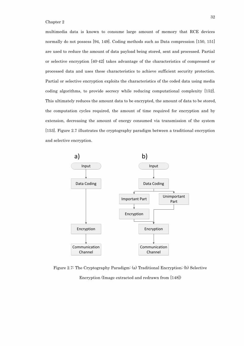
32
Chapter 2
multimedia data is known to consume large amount of memory that RCE devices
normally do not possess [94, 149]. Coding methods such as Data compression [150, 151]
are used to reduce the amount of data payload being stored, sent and processed. Partial
or selective encryption [40-42] takes advantage of the characteristics of compressed or
processed data and uses these characteristics to achieve sufficient security protection.
Partial or selective encryption exploits the characteristics of the coded data using media
coding algorithms, to provide secrecy while reducing computational complexity [152].
This ultimately reduces the amount data to be encrypted, the amount of data to be stored,
the computation cycles required, the amount of time required for encryption and by
extension, decreasing the amount of energy consumed via transmission of the system
[153]. Figure 2.7 illustrates the cryptography paradigm between a traditional encryption
and selective encryption.
Input
Data Coding
Encryption
Communication Channel
Input
Data Coding
Encryption
Communication Channel
Important PartUnimportant
Part
Encryption
a) b)
Figure 2.7: The Cryptography Paradigm: (a) Traditional Encryption; (b) Selective
Encryption (Image extracted and redrawn from [148])
33
Chapter 2
2.2.2. The Choice of Cryptographic Algorithms / Primitives
Various types of ciphers needed to be considered. Private Key Cryptography (PKC) is
considered the commonly used cryptographic primitive for WSN RCE as opposed to
Public Key Cryptography [19, 83]. There are two general types of ciphers: Symmetric and
Asymmetric ciphers. To find out the choice of cipher algorithms suitable for WSN RCE,
Law et al [19] reviews the Private Key Symmetric Block ciphers used in WSN RCE and
provided insights for security options in different resource and security requirement
scenarios. Besides the Symmetric Block ciphers, ciphers such as the Lightweight,
Involution and Stream ciphers were investigated on the suitability for RCE applications
in [6, 96, 140, 154-159]. For low-area, low-complexity applications, symmetric ciphers are
preferred due to their nature of being hardware implementation-friendly [61, 62]. Law et
al [19] concluded that the AES cipher is best suited for higher security but worst
performing in terms of memory and power consumption. On the other hand, Skipjack is a
viable option for low-security applications. Law et al [19] has also made a specification
comparison of sensors nodes, claiming that the rate of improvement is conservatively at a
lower rate than Moore's law prediction. This further confirms the need for cheaper
security designs and the conclusion reached is founded on MCU-based WSN nodes.

34
Chapter 2
2.3. Security in Multimedia Data Processing
Security for multimedia can be achieved on multimedia content using encryption
techniques. Multimedia compression [160] is often used to save cost in memory and
bandwidth. Compression is a way to discard redundant information by searching for a
less-correlated representation of an image or a video data. Compression techniques often
revolve around two concepts: spatial redundancy and temporal redundancy. Temporal
compression techniques take advantage of areas of the image that remained unchanged,
from the previous frame to the current frame. Temporal techniques focus on storing the
‘changes’ between subsequent frames rather than the entire image frame. Sequential
image or video without many changes take the best advantage of temporal compression.
Spatial compression is a technique of information reduction on a single image or frame
independent of other frames and thus, suitable for still images.
There are two type image compression algorithms: lossless and lossy compression.
Lossless, decorrelation compression technique is preferred for image application because
it removes redundancy and allows important data to be perfectly reconstructed,
especially for classified images [161]. Chew et al concluded that the Set Partitioning in
Hierarchical Tree (SPIHT) compression algorithm has the highest compression ratio and
reasonably low computation complexity, which is very suitable for WMSN or WVSN RCE
applications [162].
2.3.1. Set Partitioning in Hierarchical Trees (SPIHT) – A Lossless
Compression Technique
The set partitioning in hierarchical trees (SPIHT) algorithm by A. Said and W. A.
Pearlman [163] is a lossless-compression algorithm. SPIHT is a powerful compression
algorithm as it allows progressive reconstruction. To acquire higher quality image, more
refinement bits are required and decoding can stop at any point in the bit-stream. Ritter
et al [164] stated that Discrete Wavelet Transform (DWT) followed by Embedded

35
Chapter 2
Zerotree Wavelet (EZW) is a very efficient combination for image compression. The
SPIHT is a highly refined version of the EZW and has higher compression ration than
EZW.
The EZW coding uses the DWT to decompose an image into multi-resolution sub-bands,
creating low-frequency and high-frequency component of an image. In the wavelet sub-
bands, every coefficient at a given scale is related a set of coefficients at the next lower
scale. This relationship is often referred as the parent-children relationship in the
literatures. Each node will contain 2 by 2 children at a lower scale. At the highest scale,
the sub-band is called the LL sub-band (low-low). This LL band will have 3 children
nodes: the HL band, LH band and the HH band. Due to the nature of the wavelet
decomposition, the higher scale sub-bands will contain more energy than the lower scale
sub-bands. Thus, the embedded coding starts with the highest LL sub-band followed by
HL, LH and HH sub-bands. Figure 2.8 depicts the parent-children dependencies in EZW
coding, which is also used in the SPIHT.
HL2
HH2LH2 HL1
HH1LH1
LL
Figure 2.8: The parent-children dependencies in EZW and SPIHT (Image extracted and
redrawn from [151]).
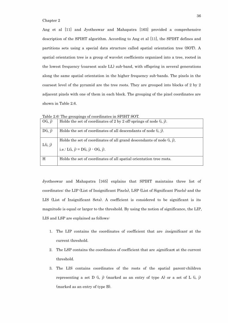
36
Chapter 2
Ang et al [11] and Jyotheswar and Mahapatra [165] provided a comprehensive
description of the SPIHT algorithm. According to Ang et al [11], the SPIHT defines and
partitions sets using a special data structure called spatial orientation tree (SOT). A
spatial orientation tree is a group of wavelet coefficients organized into a tree, rooted in
the lowest frequency (coarsest scale LL) sub-band, with offspring in several generations
along the same spatial orientation in the higher frequency sub-bands. The pixels in the
coarsest level of the pyramid are the tree roots. They are grouped into blocks of 2 by 2
adjacent pixels with one of them in each block. The grouping of the pixel coordinates are
shown in Table 2.6.
Table 2.6: The groupings of coordinates in SPIHT SOT.
O(i, j) Holds the set of coordinates of 2 by 2 off-springs of node (i, j).
D(i, j) Holds the set of coordinates of all descendants of node (i, j).
L(i, j)
Holds the set of coordinates of all grand descendants of node (i, j),
i.e.: L(i, j) = D(i, j) - O(i, j).
H Holds the set of coordinates of all spatial orientation tree roots.
Jyotheswar and Mahapatra [165] explains that SPIHT maintains three list of
coordinates: the LIP (List of Insignificant Pixels), LSP (List of Significant Pixels) and the
LIS (List of Insignificant Sets). A coefficient is considered to be significant is its
magnitude is equal or larger to the threshold. By using the notion of significance, the LIP,
LIS and LSP are explained as follows:
1. The LIP contains the coordinates of coefficient that are insignificant at the
current threshold.
2. The LSP contains the coordinates of coefficient that are significant at the current
threshold.
3. The LIS contains coordinates of the roots of the spatial parent-children
representing a set D (i, j) (marked as an entry of type A) or a set of L (i, j)
(marked as an entry of type B).

37
Chapter 2
The SPIHT algorithm can be divided into three stages: initialization, sorting and
refinement [165]. During the initialization stage, SPIHT first calculates the maximum
bit-plane level required for the coding due to maximum value in the wavelet coefficient
pyramid, and sets the start threshold for the maximum bit-plane level coding. It then
sets the LSP (significant) to an empty list and puts the coordinates of all coefficients in
the coarsest level of the wavelet pyramid into the LIP (insignificant), and those which
have descendants also, into the LIS. In the sorting pass, the algorithm first sorts the
elements of the LIP (insignificant) and then the sets with roots in the LIS.
For each pixel in the LIP (insignificant), the SPIHT performs a significance test against
the current threshold and outputs the test result to the output bit stream. The entire test
results are encoded as either 0 or 1. If a coefficient is significant, its sign is coded and
then its coordinate is moved to the LSP (significant). During the sorting pass of LIS
(insignificant), the SPIHT encoder carries out the significance test for each set in the LIS
(insignificant) and outputs the significance information. If a set is significant, it is
partitioned to its subsets according to the set-partitioning rules mentioned in the
previous subsection.
The sorting and partitioning are carried out until all significant coefficients have been
found and sorted in the LSP (significant). After the sorting pass for all elements in the
LIP (insignificant) and LIS, the SPIHT performs a refinement pass with the current
threshold for all entries in the LSP (significant), except those which have been moved to
the LSP (significant) during the last sorting pass. And lastly, the current threshold is
divided by two and the sorting and refinement stages are continued until a predefined
bit-budget is exhausted.
Ang et al [11] proposed a modified version of SPIHT using zero-tree coding (which is
termed the SPIHT-ZTR). The SPIHT-ZTR exploits the relationship among the wavelet
coefficients. The Zero-tree condition is mentioned previously that this type of SOT is
encoded with a single symbol which indicates that all the nodes in this particular SOT
are insignificant. This modified version of SPIHT provides a better implementation
38
Chapter 2
advantage for low-memory applications [11]. In the proposed SPIHT-ZTR algorithm,
significance tests performed on an individual tree node, descendant of a tree node and
grand descendant of a tree node are referred to as SIG, DESC and GDESC. Three
significant maps known as SIG_PREV, DESC_PREV and GDESC_PREV are used to
store the significance of the coefficient. During the stage for upward scanning
significance data collection (stage 2, after DWT is performed), a significance table is
generated and stored in STRIP_BUFFER, which is then used for the final stage of
SPIHT coding.
Singh et al [166] briefly describes a direct implementation of the SPIHT software
algorithm. Ritter et al [164] implemented SPIHT on a Xilinx FPGA XC4085XLA,
consuming 743 logic blocks for the design without arithmetic coding running at 40MHz
and 1425 logic blocks with arithmetic coding. Jyotheswar and Mahapatra [165] presented
an efficient FPGA implementation of DWT and modified SPIHT. Jyotheswar and
Mahapatra’s implementation results show that a total of 7021 slices used, 1439 slice flip-
flop used and a total of 13356 4 input LUTs used. The paper serves as a reference to
SPIHT hardware implementations. Vipin et al [167] presented their work on SPIHT
FPGA implementation using a SPARTAN 3E FPGA without model details. The results
were 1850 / 1920 slices, 2315 / 3840 slices Flip Flop, 2961 / 3840 4 input LUT and 4 / 12
BRAM utilized.
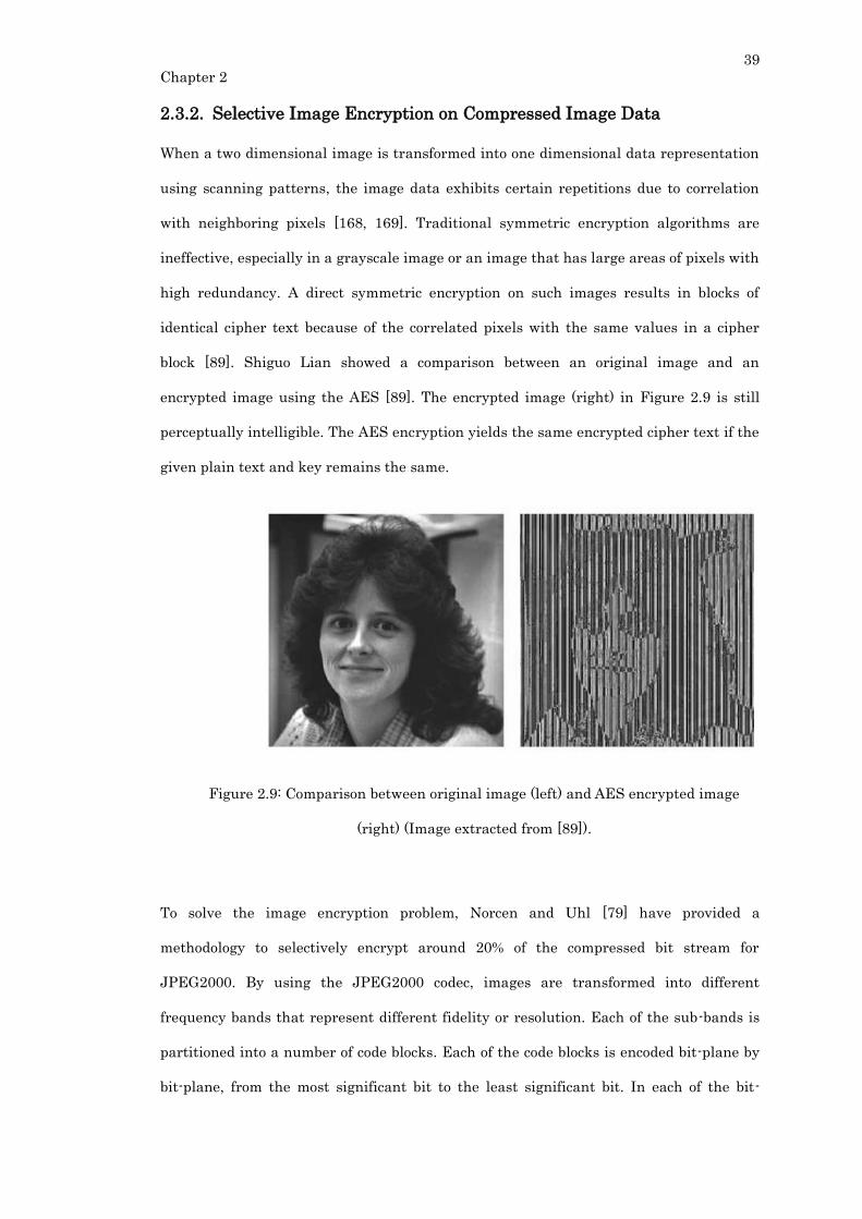
39
Chapter 2
2.3.2. Selective Image Encryption on Compressed Image Data
When a two dimensional image is transformed into one dimensional data representation
using scanning patterns, the image data exhibits certain repetitions due to correlation
with neighboring pixels [168, 169]. Traditional symmetric encryption algorithms are
ineffective, especially in a grayscale image or an image that has large areas of pixels with
high redundancy. A direct symmetric encryption on such images results in blocks of
identical cipher text because of the correlated pixels with the same values in a cipher
block [89]. Shiguo Lian showed a comparison between an original image and an
encrypted image using the AES [89]. The encrypted image (right) in Figure 2.9 is still
perceptually intelligible. The AES encryption yields the same encrypted cipher text if the
given plain text and key remains the same.
Figure 2.9: Comparison between original image (left) and AES encrypted image
(right) (Image extracted from [89]).
To solve the image encryption problem, Norcen and Uhl [79] have provided a
methodology to selectively encrypt around 20% of the compressed bit stream for
JPEG2000. By using the JPEG2000 codec, images are transformed into different
frequency bands that represent different fidelity or resolution. Each of the sub-bands is
partitioned into a number of code blocks. Each of the code blocks is encoded bit-plane by
bit-plane, from the most significant bit to the least significant bit. In each of the bit-

40
Chapter 2
planes, there are mapping and refinement bits. By encrypting the mapping bits, an
image reconstructed from the cipher text is unintelligible. Lian et al [80] suggested that
only the significant bits are selected for AES encryption. Figure 2.10 shows the original
‘Peppers’ JPEG2000 image (a) and the encrypted image (b). And (c) is the JPEG2000
‘Plane’ image coupled with its encrypted image (d). The encrypted images are
perceptually unintelligible and therefore secured, showing that the AES symmetric
cipher is able to work in combination with compression schemes. Figure 2.11 shows the
general idea of a working selective encryption system, which comprises of encryption and
decryption processes.
Figure 2.10: The results of encrypting JPEG2000 coded images using AES (Image
extracted from [89]).
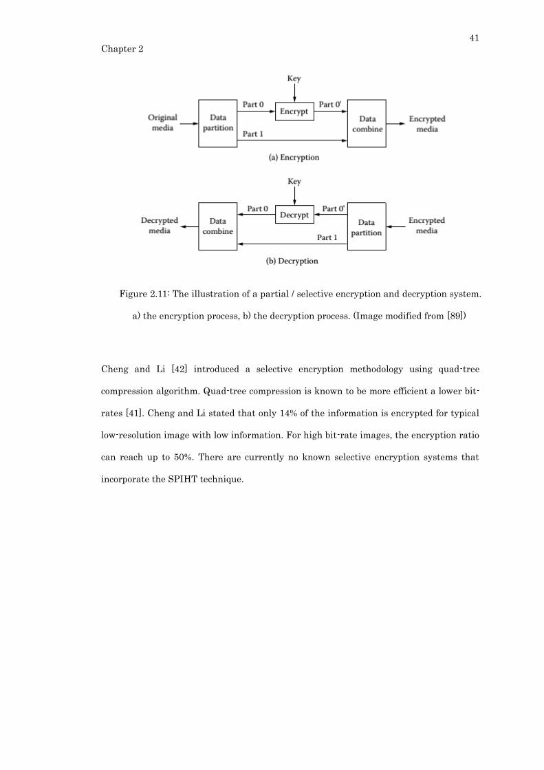
41
Chapter 2
Figure 2.11: The illustration of a partial / selective encryption and decryption system.
a) the encryption process, b) the decryption process. (Image modified from [89])
Cheng and Li [42] introduced a selective encryption methodology using quad-tree
compression algorithm. Quad-tree compression is known to be more efficient a lower bit-
rates [41]. Cheng and Li stated that only 14% of the information is encrypted for typical
low-resolution image with low information. For high bit-rate images, the encryption ratio
can reach up to 50%. There are currently no known selective encryption systems that
incorporate the SPIHT technique.
42
Chapter 2
2.4. Crypto-processor for RCE Application
The ideal crypto-processor to face multiple RCE security threats [31], must be capable of
double or multiple encryption [27, 28], multi-cipher [29], support for cipher mode of
operation [30], multi-level security [31], key management [32], authentication [33], and
digital signature. Such a crypto-processor has to have diverse security features and
functions.
2.4.1. Crypto-processors for Multi-cipher Application
Multiple security protocols requires multiple cryptographic primitives, leading to the
need of multiple cryptographic primitive cores [34]. Multiple primitive cores increase the
hardware area memory requirement due to cipher programs and crypto-specific
instruction sets. A unified crypto-processor [170] is able to operate and perform multiple
ciphers, removing the need for separate cryptographic cores and the hardware logic
needed for those cores. The only cost for this configuration would be the cipher’s program
that occupies the memory. More cipher programs require more memory.
‘Multi-level security’ (MLS) or ‘Multi Security Levels’ (MSL) [171] refers to a security
environment in which there are different communication access and clearance levels,
which are dependent on the strength of cryptographic algorithm used. Jongdeog et al
[171] stated that having more powerful algorithms for higher security domains would be
reasonable as security levels correspond to sensitivity and clearance. Due to the resource
limitations of RCE sensor nodes, strong cipher algorithms may consume more memory
and energy. A low level security domain may opt to use a light encryption algorithm
rather than a heavy one provided that there are multi cryptographic primitives to choose
from [171]. A stronger crypto-solution would provide a higher clearance (for decryption
and access) [76, 172]. A multi-level secure framework is able to support secure
communication between nodes in a network instead of using a static solution to a wide
spectrum of threats [172]. Afzal et al [172] stated that WSN RCE security protocols
43
Chapter 2
achieve secure communication by using digital signatures, authentication schemes,
symmetric keying and asymmetric keying. To ensure data non-repudiation, timestamps,
random number generators and initialization vector are used in conjunction with
security schemes. However, Afzal et al also stated that WSN RCE security schemes are
static and coarse, that are unable to impose multiple level of clearances to limit access to
parts or components of the node device. The other proposals on multi-level solutions are
predominantly on the node cluster level [76, 172, 173], forming frameworks models and
security topology by enforcing or manipulating information flow. One way to impose
security and access control is the use of authentication using Cipher Block Chaining
(CBC) and Cipher Block Chaining - Message Authentication Code (CBC-MAC), which
requires symmetric key cryptographic functions. The underlying basis for a well-
designed crypto-processor is the ability to provide sufficient cryptographic functions to
formulate robust protocols and schemes. Regardless of the requirements of a multi-cipher
or a multi-level system, the apparent solution to a well–designed, flexible crypto-
processor is having multiple cryptographic functions.
The CryptoManiac [78] processor is a flexible crypto-coprocessor which supports multiple
cipher algorithms and also multi-mode operations. Lavos et al [174] has stated that the
ECB (Electronic Cook Book) mode for symmetric ciphers are the most common mode of
operation used. Lavos et al also states that the more ‘mode of operations’ that one crypto-
system can support, the more robust and more flexible it is to suit the current needs and
applications. There are a few modes of operations other than the ECB worth mentioning
and they are: cipher block chaining (CBC), cipher feedback (CFB), counter (CTR), and
output feedback (OFB). Lavos et al also proposed a reconfigurable crypto processor
design to accommodate various encryption algorithms and their respective mode of
operation with the ultimate aim to provide a unified platform with a design that houses
the configuration for multi-mode applications. Lavos et al presented an inner-
architecture that focuses on the Cipher Block Unit, using loop-rolling architecture for
smaller code size. Five ciphers were presented by the Lavos et al: AES, IDEA, DES, RC5,
and SAFER+, showing a great selection of cipher implementations. Figure 2.12 shows
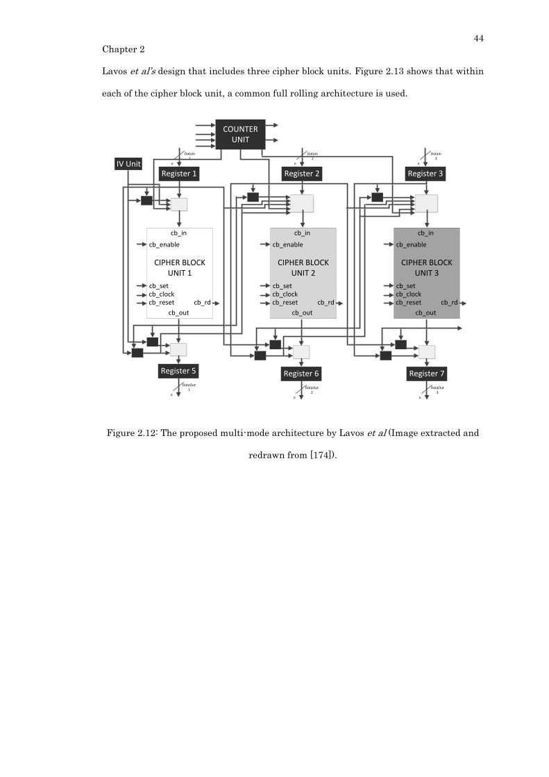
44
Chapter 2
Lavos et al’s design that includes three cipher block units. Figure 2.13 shows that within
each of the cipher block unit, a common full rolling architecture is used.
COUNTER UNIT
IV Unit
cb_in
cb_enable
cb_clockcb_set
cb_reset
cb_out
cb_rd
CIPHER BLOCK UNIT 2
cb_in
cb_enable
cb_clockcb_set
cb_reset
cb_out
cb_rd
CIPHER BLOCK UNIT 3
cb_in
cb_enable
cb_clockcb_set
cb_reset
cb_out
cb_rd
CIPHER BLOCK UNIT 1
Register 5
n
DataOut1
Register 6
n
DataOut2
Register 7
n
DataOut3
n
DataIn1
Register 1 Register 2
n
DataIn2
n
DataIn3
Register 3
Figure 2.12: The proposed multi-mode architecture by Lavos et al (Image extracted and
redrawn from [174]).
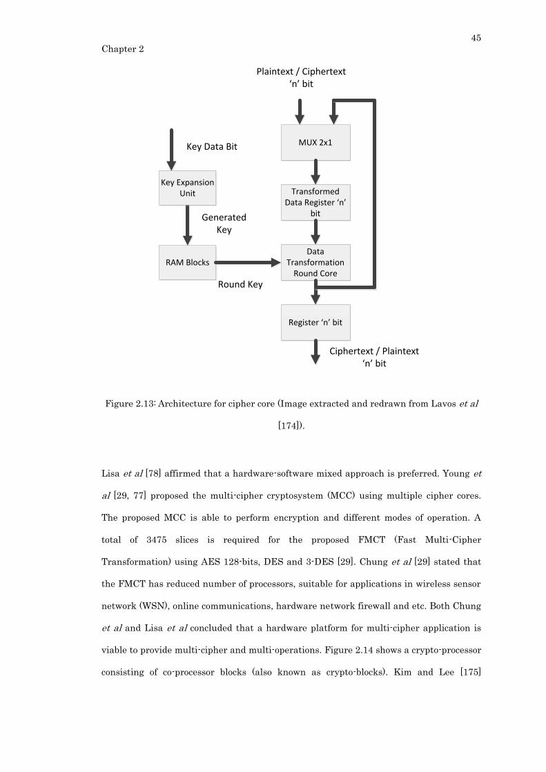
45
Chapter 2
Key Expansion Unit
Key Data Bit
Generated Key
RAM Blocks
Round Key
Transformed Data Register ‘n’
bit
Data Transformation
Round Core
Register ‘n’ bit
Ciphertext / Plaintext ‘n’ bit
Plaintext / Ciphertext ‘n’ bit
MUX 2x1
Figure 2.13: Architecture for cipher core (Image extracted and redrawn from Lavos et al
[174]).
Lisa et al [78] affirmed that a hardware-software mixed approach is preferred. Young et
al [29, 77] proposed the multi-cipher cryptosystem (MCC) using multiple cipher cores.
The proposed MCC is able to perform encryption and different modes of operation. A
total of 3475 slices is required for the proposed FMCT (Fast Multi-Cipher
Transformation) using AES 128-bits, DES and 3-DES [29]. Chung et al [29] stated that
the FMCT has reduced number of processors, suitable for applications in wireless sensor
network (WSN), online communications, hardware network firewall and etc. Both Chung
et al and Lisa et al concluded that a hardware platform for multi-cipher application is
viable to provide multi-cipher and multi-operations. Figure 2.14 shows a crypto-processor
consisting of co-processor blocks (also known as crypto-blocks). Kim and Lee [175]

46
Chapter 2
implemented both private and public key primitives with a VLSI chip using 0.5µm
CMOS and their AES implementation utilizes 1689 logic slices operating at 58 MHz.
Figure 2.14: Architecture of a multiple cryptographic primitives / processors forming a
robust crypto-processor (Image extracted from [175])
In a multi-core environment, besides having multiple cipher cores, one advantage having
identical cipher cores is to improve a system’s throughput [35, 176-178]. Identical cipher
cores can exist if design is configured to do so with the help of reconfigurable hardware.
Feng et al [179] concluded that using identical cryptographic functions with different key
(based on the survey on security FPGA crypto-design by Drimer [180]), the noise
contributed by the concurrent processes can be removed. Noise from concurrent processes
enables attackers to obtain a correlation model hence risking the system. The
architecture proposed by Feng et al [179] uses a NEW key pairing algorithm to create
new key-pairings (2 sets of keys) instead of injecting 2 different keys directly. Feng et al
proposed a tweaked version of AES hardware implementation that uses two sets of keys
(namely the duo key AES). In an encryption process, if a plaintext is encrypted using 2
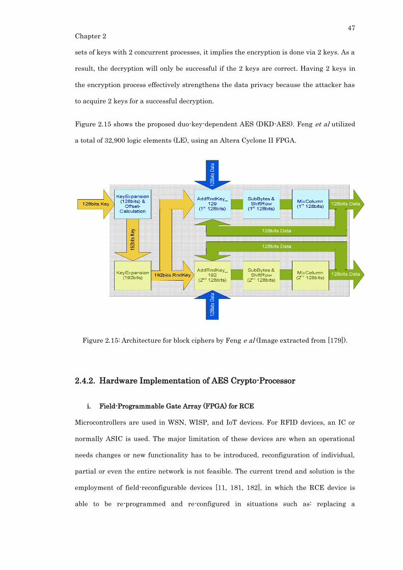
47
Chapter 2
sets of keys with 2 concurrent processes, it implies the encryption is done via 2 keys. As a
result, the decryption will only be successful if the 2 keys are correct. Having 2 keys in
the encryption process effectively strengthens the data privacy because the attacker has
to acquire 2 keys for a successful decryption.
Figure 2.15 shows the proposed duo-key-dependent AES (DKD-AES). Feng et al utilized
a total of 32,900 logic elements (LE), using an Altera Cyclone II FPGA.
Figure 2.15: Architecture for block ciphers by Feng e al (Image extracted from [179]).
2.4.2. Hardware Implementation of AES Crypto-Processor
i. Field-Programmable Gate Array (FPGA) for RCE
Microcontrollers are used in WSN, WISP, and IoT devices. For RFID devices, an IC or
normally ASIC is used. The major limitation of these devices are when an operational
needs changes or new functionality has to be introduced, reconfiguration of individual,
partial or even the entire network is not feasible. The current trend and solution is the
employment of field-reconfigurable devices [11, 181, 182], in which the RCE device is
able to be re-programmed and re-configured in situations such as: replacing a
48
Chapter 2
compromised cryptographic primitive, upgrading system’s performance, reconfiguration
for a new purposes, hardware bug fixes, and updates. Ultimately, RCE devices employing
field-programmable hardware is the new platform [9, 12, 183, 184]. Complex image,
video and multimedia processing is feasible using FPGA [185-187]. Thus, allowing visual
processing and security to co-exists, forming a robust and secure visual sensor network.
A typical Xilinx FPGA chip contains a fixed amount of resource elements referred to as a
slice. A slice is made up of look-up tables (LUTs) and D-type flip-flops (FDs). Thus, the
area utilization of a design using Xilinx FPGA technology is quoted in terms of the
amount of slices used.
ii. Low-area Architecture for AES Processors
The AES has four basic steps in each round of encryption. The four steps, in order, are
called SubBytes (also known as the byte substitution), ShiftRows, MixColumns, and
AddRoundKey. The description of the four basic steps in AES rounds are:
AddRoundKey: A simple transformation performs XOR with the sub key to the
round state.
ShiftRow: Shifts the byte location with the offset from zero to three depending on
the row location.
MixColumns: Column vector is multiplied with a fixed matrix where bytes are
treated as polynomials.
SubBytes: Non-linear byte substitution which is composed of multiplicative
inverse, affine transformation and inverse affine transformation.
In terms of hardware design, there are typically three types of AES hardware
architecture [188]:
1) Looping Architecture.
2) Fully unrolled pipelined architecture.
3) Deep sub-pipelined fully unrolled architecture.
49
Chapter 2
Among the three types above, Looping Architecture is known to be efficient on hardware
area utilization [189-191]. For high throughput applications, the architectural design
usually inclines towards unrolling the loops within AES with the help of a deeply
pipelined 128-bit data path [93]. This technique however would require excessive
hardware area and power which RCE devices unable to afford. Hence, low-area, low-
power designs are preferred in RCE.
There are numerous AES designs aiming for low-area architectures for constrained
FPGA environment [189, 191-193]. Among the low-area designs, Rouvroy et al [191] and
Chodiwiec et al [189] has the best low-area results. Rouvroy et al [191] reported a total of
146 slices utilized on a XC2S40-6 FPGA and Chodiwiec et al [189] reported a total of 522
equivalent slices utilized on a Xilinx XC2S30-6 FPGA. Both Rouvroy et al and Chodiwiec
et al use a fixed-width 32-bit data-path, which leads to a significant drop in terms of
throughput as compared to a fully-unrolled 128-bit data path. Feldhofer et al [192] was
the first to propose a design using an 8-bit data-path, claiming to have the smallest area
to date. Goodman et al [190] proposed using a customized application-specific 8-bit data-
path architecture to further lower the design area and is currently known to have the
smallest design on FPGA (122 slices using Spartan-II XC2S15-6).
Goodman et al [190] stated three key design aspects of an AES processor that
contributed to most of the logic area:
1) The S-box computation.
2) The definition of a suitable primitive operation.
3) Cipher’s programs size.
From the architectural point of view, Goodman et al ‘s low-area AES has the following
key features to reduce area:
a) Generate expanded keys (forward and inverse keys) on the fly using forward
expansion and a proposed inverse expansion without saving all the expanded
keys.
50
Chapter 2
b) The calculation of the S-box is done via 5 clock cycles (multiplicative inverse
requires 3 clock cycles, sharing the same multiplier) to reduce hardware area.
c) A very basic processing architecture that performs primitive operations such as
moving 8-bit data, finite-field multiply by 2 (ffm2), finite-field division by 2 (ffd2)
and XOR are used.
d) Instruction decoder is minimized by including only the required instruction sets
(15 instructions).
e) Programming techniques such as sub-routines and iterations are used (two
levels).
Goodman et al ‘s design is highly tailored and specific to AES. The use of the most
fundamental or primitive arithmetic operations is effective in reducing the complexity of
the processor’s core at the cost of throughput. Hence the term application specific
integrated processor (ASIP) is used to describe the design.
However, Goodman et al ‘s design has a few drawbacks when RCE application is consider.
An ASIP design of AES is rigid and lacks flexibility. The ASIP hardware data-path and
finite-state machine (FSM) cannot be reused or repurposed because it is designed to
perform only a single task. Resources in RCE are extremely scarce, forcing system
designers to reuse or repurpose processors to facilitate adaptation to observed
environmental changes or to cater to changing priorities [194]. Hence, general-purpose
processors are more popular in the RCE. Some may argue that RCE devices do not need
flexibility but the very nature of RCE devices being pervasive and ubiquitous, requires
flexibility and scalability to face increasing communication and security demands [195].
ASIP is a good design for hardware acceleration by doing a single, specific task efficiently.
RCE application requires improvisation in the face of changing environments where RCE
devices usually make do with the limited resources given.
The primitive operations used in ASIP AES are great in reducing computation
complexity considering that ASIP AES only runs AES. These primitive finite-field
operations are highly specific to AES. Hardware implementation of ffm2 and ffd2 are
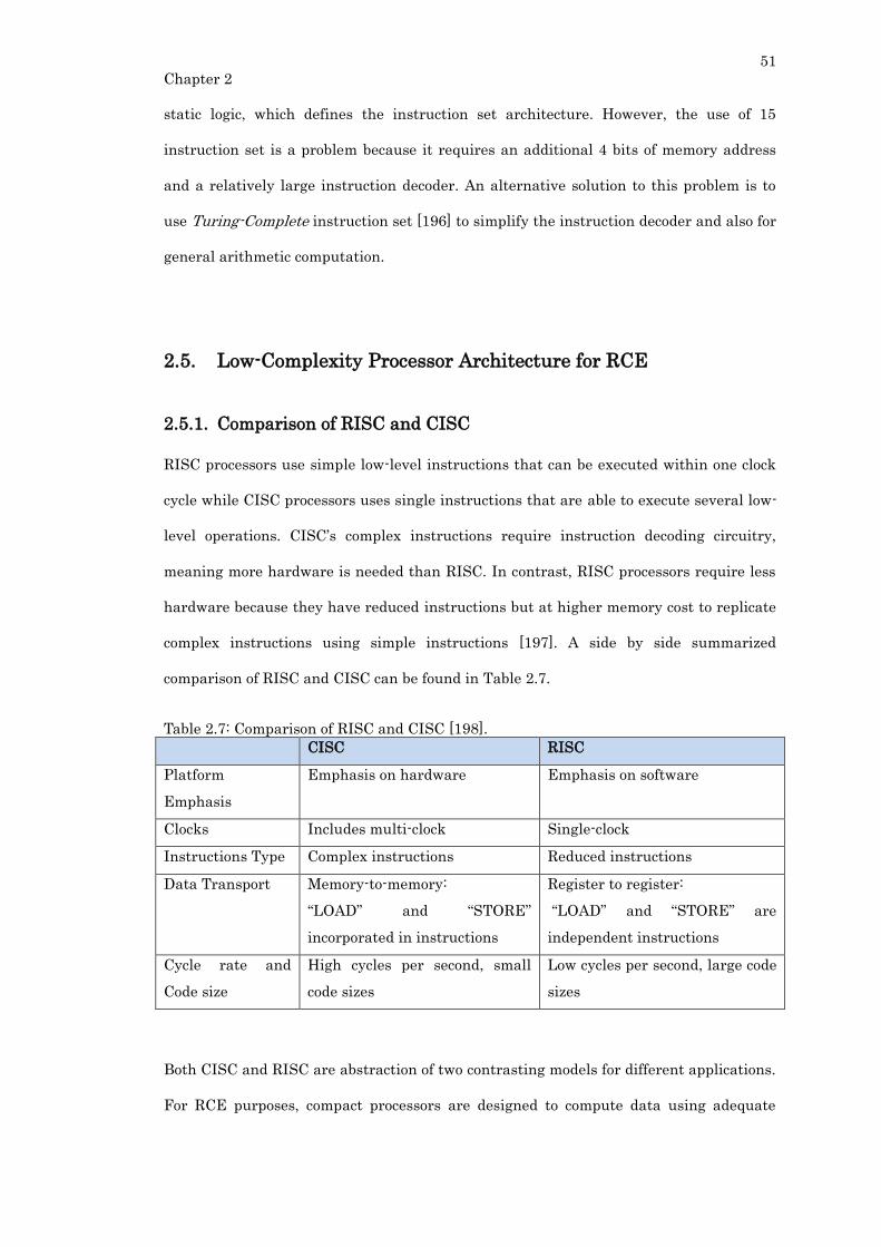
51
Chapter 2
static logic, which defines the instruction set architecture. However, the use of 15
instruction set is a problem because it requires an additional 4 bits of memory address
and a relatively large instruction decoder. An alternative solution to this problem is to
use Turing-Complete instruction set [196] to simplify the instruction decoder and also for
general arithmetic computation.
2.5. Low-Complexity Processor Architecture for RCE
2.5.1. Comparison of RISC and CISC
RISC processors use simple low-level instructions that can be executed within one clock
cycle while CISC processors uses single instructions that are able to execute several low-
level operations. CISC’s complex instructions require instruction decoding circuitry,
meaning more hardware is needed than RISC. In contrast, RISC processors require less
hardware because they have reduced instructions but at higher memory cost to replicate
complex instructions using simple instructions [197]. A side by side summarized
comparison of RISC and CISC can be found in Table 2.7.
Table 2.7: Comparison of RISC and CISC [198].
CISC RISC
Platform
Emphasis
Emphasis on hardware Emphasis on software
Clocks Includes multi-clock Single-clock
Instructions Type Complex instructions Reduced instructions
Data Transport Memory-to-memory:
“LOAD” and “STORE”
incorporated in instructions
Register to register:
“LOAD” and “STORE” are
independent instructions
Cycle rate and
Code size
High cycles per second, small
code sizes
Low cycles per second, large code
sizes
Both CISC and RISC are abstraction of two contrasting models for different applications.
For RCE purposes, compact processors are designed to compute data using adequate
52
Chapter 2
components. Adapting a CISC or RISC model for a crypto-processor has some trade-offs.
CISC is not a suitable model for RCE because of the instruction decoder and RISC is not
suitable for RCE due to larger code size. Both models are relatively complex machines
that serve general computing purposes.
2.5.2. One Instruction Set Computer (OISC), also known as the Ultimate
Reduced Instruction Set Computer (URISC)
A one instruction set computer (OISC), also known as the ultimate reduced instruction
set computer (URISC) in [196], is an abstract machine that uses only a single instruction.
Given infinite resources, an URISC is said to be capable of being a universal computer in
the same manner as traditional computers that have multiple instructions [54]. The
URISC is also consider Turing-Complete because of its ability to perform all
computations using a single instruction [55, 59].
Currently, there three known URISC categories [199]:
1) Transport Triggered Architecture Machines
2) Bit Manipulating Machines
3) Arithmetic based Turing-Complete Machines
Arithmetic based Turing-Complete Machines are universal and Turing-Complete [199].
They are considered most practical because they consist of a conditional jump operation.
Tsoutsos et al [60] stated that common Turing-Complete variants such as ‘add and
branch unless positive’ (ADDLEQ), ‘subtract and branch if negative’ (SUBLEQ) and ‘plus
one and branch if equal’ (P1EQ) have a common pattern of a simple mathematical
operation followed by a conditional jump. The SUBLEQ is the oldest and also the most
efficient and popular arithmetic operation [200].
The URISC has two models: ‘Subtract and Branch if Negative’ (SBN) and MOVE [54].
The comparison of the URISC SBN and URISC MOVE models can be found in Table 2.8.
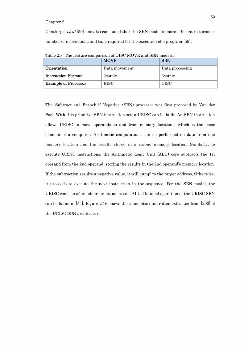
53
Chapter 2
Chatterjee et al [59] has also concluded that the SBN model is more efficient in terms of
number of instructions and time required for the execution of a program [59].
Table 2.8: The feature comparison of OISC MOVE and SBN models.
MOVE SBN
Orientation Data movement Data processing
Instruction Format 2-tuple 3-tuple
Example of Processor RISC CISC
The ‘Subtract and Branch if Negative’ (SBN) processor was first proposed by Van der
Poel. With this primitive SBN instruction set, a URISC can be built. An SBN instruction
allows URISC to move operands to and from memory locations, which is the basic
element of a computer. Arithmetic computations can be performed on data from one
memory location and the results stored in a second memory location. Similarly, to
execute URISC instructions, the Arithmetic Logic Unit (ALU) core subtracts the 1st
operand from the 2nd operand, storing the results in the 2nd operand’s memory location.
If the subtraction results a negative value, it will ‘jump’ to the target address, Otherwise,
it proceeds to execute the next instruction in the sequence. For the SBN model, the
URISC consists of an adder circuit as its sole ALU. Detailed operation of the URISC SBN
can be found in [54]. Figure 2.16 shows the schematic illustration extracted from [200] of
the URISC SBN architecture.
54
Chapter 2
ADDER
PC
Z N
R
MDR
MAR
PC out PC in
R in
Z in
N in
MDR out MDR in
MAR in
C in
MEMORY
READ
WRITE
COMP
Figure 2.16: The URISC SBN architecture with Adder (Image extracted from [200]).
In terms of real-world application, URISC was recommended as the material for teaching
computer architecture to students, giving them the basic understandings of hardware
and software co-design abstraction [54, 196]. Despite URISC’s sheer simplicity with no
implication of complex applications, the URISC has been used in ‘homomorphic
encryption’ systems for cloud computing, namely the Fully Homomorphic Ultimate RISC
(FURISC) [59]. The justification for security application is that cloud computing requires
direct computation on encrypted data and also the need to develop secured encrypted
processors in which both data and instructions are also encrypted. It is logical to assume
that with only a single instruction, complex processing overhead is high. This is further
validated by [201, 202]. The Homomorphically Encrypted One Instruction Computer
(HEROIC) [60] is also a similar processor with the FURISC, showing that URISC is
gaining popularity because a single instruction architecture is able to offer security for
the program and data within the system. Both of these designs are rooted on the fact
55
Chapter 2
that URISC lacks multiple instructions and opcodes, which is the biggest advantage in
maintaining the confidentiality of the instruction and algorithm [60]. In the area of
security, FURISC [59] and HEROIC [60] shows that URISC is feasible thus showing
potential.
2.5.3. Minimal Instruction Set Computer (MISC)
Minimal Instruction Set Computer (MISC), differs from URISC, in having multiple
instructions sets within an Instruction Set Architecture (ISA). A MISC is a computer
having a minimal amount of instruction sets, sufficient for its purpose. The concept of
such a computer is to have only the essential computing blocks to form a functional
computer, without any unnecessary parts or blocks. Hence the term “minimal” is used for
the basic behavior of such a processor.
Although URISC with a single instruction is Turing-Complete, the number of
instructions required for a meaningful operation is staggering, leading to a very high
overhead as mentioned in the section 2.5.2. A URISC can be configured to become a
MISC with additional opcodes and ALUs.
The work by Ting and Moore [203] states that reducing the size of the instruction set is
effective in reducing the complexity of the process thus improving its performance. Ting
and Moore understand that there are three important issues when designing a MISC for
a particular application:
1) What is the minimum set of instructions required for a processor to be practical
in solving specific problems?
2) What will be the performance of the said MISC?
3) What facilities within a processor are necessary to reduce the complexity and the
system costs of the said MISC?

56
Chapter 2
Understand these three issues will help in producing a minimalist computer. However,
compared to URISC, the MISC has added complexity. The additional ALUs and
instructions lead to additional hardware costs hence illustrating point 2) and 3). The
trade-off between complexity and hardware cost has to be made.

57
Chapter 2
2.6. The AES Cipher and the Non-linear S-Box (Sub-bytes)
In general, the S-Box (also known as Sub-bytes within AES transformations) is unique
because it is the only non-linear step in the AES encryption. The S-Box functions as
replacing or substituting an input with another byte. Traditionally, implementation
approach is preferred to storing the values of the S-Box into a ROM and uses it as a
Look-up Table. Earlier versions of the S-box circuit are in 8-by-8 Look-up tables and can
be found in these proposals: [204, 205]. Table 2.9 shows an illustration of the S-box Look-
up Table with 256 values.
Table 2.9: The lookup table of the 256 substitution values for S-box. 0 1 2 3 4 5 6 7 8 9 A B C D E F
0 63 7C 77 7B F2 6B 6F C5 30 01 67 2B FE D7 AB 76
1 CA 82 C9 7D FA 59 47 F0 AD D4 A2 AF 9C A4 72 C0
2 B7 FD 93 26 36 3F F7 CC 34 A5 E5 F1 71 D8 31 15
3 04 C7 23 C3 18 96 05 9A 07 12 80 E2 EB 27 B2 75
4 09 83 2C 1A 1B 6E 5A A0 52 3B D6 B3 29 E3 2F 84
5 53 D1 00 ED 20 FC B1 5B 6A CB BE 39 4A 4C 58 CF
6 D0 EF AA FB 43 4D 33 85 45 F9 02 7F 50 3C 9F A8
7 51 A3 40 8F 92 9D 38 F5 BC B6 DA 21 10 FF F3 D2
8 CD 0C 13 EC 5F 97 44 17 C4 A7 7E 3D 64 5D 19 73
9 60 81 4F DC 22 2A 90 88 46 EE B8 14 DE 5E 0B DB
A E0 32 3A 0A 49 06 24 5C C2 D3 AC 62 91 95 E4 79
B E7 C8 37 6D 8D D5 4E A9 6C 56 F4 EA 65 7A AE 08
C BA 78 25 2E 1C A6 B4 C6 E8 DD 74 1F 4B BD 8B 8A
D 70 3E B5 66 48 03 F6 0E 61 35 57 B9 86 C1 1D 9E
E E1 F8 98 11 69 D9 8E 94 9B 1E 87 E9 CE 55 28 DF
F 8C A1 89 0D BF E6 42 68 41 99 2D 0F B0 54 BB 16
From a crypto-processor’s point-of-view, the AddRoundKey, ShiftRow, and MixColumns
transformations are seen as data movement and logical XORs operations. Other than S-
Box, the other three transformations are considered modulo 2 bit-wise calculations,
which can be easily implemented. However, while implementing the AES, there are a
variety of approaches to satisfy certain design criteria. For high throughput applications,
Satoh et al [206] presented 10 Gbps AES design. On the other hand, [207] proposed low-
58
Chapter 2
power AES design with energy efficient S-box circuitry. Lastly, for area-constrained
hardware applications (such as the re-configurable RCE), [68, 189, 208] presented their
findings in small S-Box circuits. To design a smaller representation of the S-Box, Rijmen
et al [65, 209, 210] suggested using sub-field arithmetic in computing the inverse in the
Galois Field of 256 elements of the S-Box. This leads to the reduction of 8-bit calculations
to several 4-bits ones, which results to smaller circuitry. Therefore, minimizing the S-Box
circuitry leads low-area hardware implementations [69].
In [68], the proposed S-Box is derived from the multiplicative inverse over Galois Field
(28). To avoid attacks based on simple algebraic properties, the S-box is constructed by
combining the inverse function with an invertible affine transformation (a matching
inverse affine is included in the decryption). Satoh et al [68] further extended this idea,
using the tower-field approach of Paar’s [211] by suggesting that breaking up the 4-bit
calculations into 2-bit variable will result to even smaller circuit blocks. Being derived
from the multiplicative inverse over Galois Field (28), the S-Box projects good non-
linearity and may have high hardware complexities. This S-Box representation gives a
higher impact since the implementation is small enough to allow unrolling or parallel
designs, for higher throughput if necessary. In the next sections, various models and
implementations of small AES S-box are reviewed.
2.6.1. The Minimized S-box by Boyar et al
In practice, circuit designs are built using numerous heuristics which potential led to
exponential time complexity which can only be applied onto small-sized circuits. The
heuristic approach naturally works fine on circuit function that can be broken down into
sub-functions, i.e. matrix multiplication, which decomposes into smaller sub-matrix
multiplications. The initial work from Boyar et al [212] is to propose a new logic
minimization technique, which can be applied to any arbitrary combinational logic
problems and even circuits that has been optimized by standard methodologies. Boyar et
al described their techniques as a two-step process: non-linear gate reduction and linear

59
Chapter 2
gate reduction. It is by far the smallest S-box combinational circuit that they have come
up with. In this section, the Boyar’s first approach in logic minimization is reviewed and
more details can be found in [212] and his improved work for an even smaller
bidirectional S-box circuit in [71].
Boyar et al explained the circuit produced for the inverse in GF (2m) suggested in [213],
has a tower fields architecture. Since there is multiple representation of Galois Fields,
there would be multiple versions of efficient circuits. Boyar’s approach is to focus on the
technique for GF (24) inversion computation and then further perform linear-circuit’s
reduction with the inversion circuit placed in a suitable position within the S-box. The
first step consists identifying the non-linear components and reducing the AND gates.
Boyar et al choses to focus on reducing only the GF (24) circuit since it would be
significantly beneficial. At the end, an inversion in GF (24) with only five AND gates
poses as a highly plausible improvement than Paar’s [211].
The second part would be focusing on minimizing linear components with their newly
proposed heuristics. Hence, Boyar et al presented two matrices U and B for linear-
minimization. The AES's S-box is S(x) = B * F(U * x) + [11000110]T, where * is matrix
multiplication and x is the 8-bit S-box input. Note that the initial linear expansion and
the linear contraction (matrix U and B) were defined to contain as much of the circuit as
possible while still maintaining linearity. Thus, Boyar et al explained that the portion of
the circuit defined by U, overlaps with the GF (28) inversion. So, the true aim in the
second part is to minimize the circuits for computing U and B. The matrix U and B is
shown in Equation [6.1] and Equation [6.2].

60
Chapter 2
𝑈 =
[ 0 0 0 0 0 0 0 10 1 1 0 0 0 0 11 1 1 0 0 0 0 11 1 1 0 0 1 1 10 1 1 1 0 0 0 10 1 1 0 0 0 1 11 0 0 1 1 0 1 10 1 0 0 1 1 1 11 0 0 0 0 1 0 01 0 0 1 0 0 0 01 1 1 1 1 0 1 00 1 0 0 1 1 1 01 0 0 1 0 1 1 01 0 0 0 0 0 1 00 0 0 1 0 1 0 01 0 0 1 1 0 1 00 0 1 0 1 1 1 01 0 1 1 0 1 0 01 0 1 0 1 1 1 00 1 1 1 1 1 1 01 1 0 1 1 1 1 01 0 1 0 1 1 0 0]
[6.1]
𝐵 =
[ 0 0 0 1 1 0 1 1 0 1 1 0 0 0 0 1 1 01 1 0 0 0 0 1 1 0 1 1 0 0 0 0 1 1 01 0 1 0 0 0 1 0 1 0 0 0 1 0 1 1 0 11 1 0 1 1 0 0 0 0 1 1 0 0 0 0 1 1 00 1 1 0 1 1 0 0 0 1 1 0 0 0 0 1 1 01 0 1 1 1 0 0 1 1 0 1 1 1 0 1 1 1 00 0 0 0 1 1 0 1 1 0 0 0 1 1 0 1 1 01 0 1 1 0 1 0 0 0 0 0 0 1 1 0 1 1 0]
[6.2]
The Boyar’s technique has yielded a circuit for the AES S-box composed of three primary
parts: the top-linear transformation, the middle non-linear block and the bottom-linear
transformation [212]. The top-linear transformation is a result of the minimized matrix
U, a total of 23 XOR gates used and at depth 7, consisting 8 inputs and 22 outputs. The
middle non-linear block is block with 22 inputs and 18 outputs, having a total of 30 XOR
and 32 AND gates. And lastly the bottom-linear block converts the 18 inputs from the
middle non-linear block to become 8-bits output, having 26 XOR and 4 XNOR gates. All

61
Chapter 2
these 3 blocks together forms the final circuit of the S-box. Boyar et al [212] presented
the forward version of the S-box, with a total gate count of 115 gates. The Figure 2.17
illustrates of the proposed S-box by Boyar et al [212].
δ (matrix U) δ-1(matrix B) GF-1
The Original Proposed SBOX (forward)
(115 gates)
Middle non-linear blockBottom Linear
BlockTop Linear Block
23 gates 62 gates 30 gates
Figure 2.17: The illustration of Boyar’s minimized S-box.
To further improve the work, the Boyar et al have presented their extensively improved
work in [71]. The Boyar’s work has proposed a more complete S-box example, by
incorporating the reversed version of the S-box. This time, Boyar attempts to apply a
greedy heuristic approach for linear-minimization and several depth reduction
techniques.
The largest circuit component is the top and bottom linear-circuits. As explained
previously, the top and linear components contain more than just the linear operations in
the definition of the complete AES S-box. The reason is that the matrices include some of
the field inversion operations. This shows that there would be some amount of AND
gates within the U and B matrices. In addition, Boyar et al stated that circuits with
fewer AND gates will have larger linear components. This part of the work is optimized
on top of the previously minimized circuit (115 gates).
Boyar et al ‘s technique is to modify a greedy heuristic approach by Paar’s [211]. Paar’s
technique keeps a list of XOR computed variable. Then the steps are repeated to search
for the XOR pair of the input which results to the most occurrences in the output. This
result is added as a new set of variable to the next stage and repeated until all the most
occurred pairs are found. Hence, the Low_Depth_Greedy algorithm only allows the

62
Chapter 2
Paar’s greediness as long as the circuit’s depth is not increased unnecessarily. Boyar et al
performed the three types of depth-reduction optimizations: 1) applying a greedy
heuristics to re-synthesize linear components into lower-depth construction of circuits, 2)
using techniques from automatic theorem proving to re-synthesize non-linear
components and 3) doing simple depth-reduction along critical paths.
The optimization results have yielded a forward S-box with 128 gates and an inverse S-
box with 127 gates. This is considered a significant improvement since the total gate
count for a complete bi-directional S-box is amounted to 192 gates, which is less than the
total gate count of the two circuits combined. From our understandings, the only tradeoff
is; to combine both circuits, a multiplexer would be required to switch between
encryption and decryption since there is a middle-shared component. Figure 2.18 shows
the illustration of the bi-directional S-box in block diagram form [71].
δ δ-1
GF-1
The Latest Proposed SBOX (bi-direction)
(192 gates)
Middle non-
linear block
(shared)
Bottom Linear
Block
Top Linear
Block
δ
MUX
MUX
27 gates
27 gates
38 gates
37 gates
63 gates
forward forward
inverse inverseδ-1
Figure 2.18: The illustration of Boyar’s recent minimized S-box (both forward and
inverse S-box).
2.6.2. The Optimized S-Box by Satoh and the Model Implementation by
Edwin
The Rijndael architecture presented by Satoh et al [68] has been a benchmark for
compact AES design for quite a period. Satoh et al proposed further optimization of the

63
Chapter 2
S-box by introducing a new composite field. Satoh et al adopted the three stage
methodology: extension field – composite field – extension field. Satoh et al suggested
that the composite field can be constructed without applying a single degree-of-8
extension to GF (2), but by applying multiple extensions of smaller degrees. Satoh et al
built the composite field by repeating the degree-of-2 extensions under the polynomial
basis with the irreducible polynomials shown in Equation [6.3] and hence, proposed a
compact architecture with the introduction of a new composite field of GF (((22)2)2) and
has shown improvement over proposals using the GF ((24)2) field approach.
{
GF(22) ∶ x2 + x + 1
GF((22)2) ∶ x2 + x + ∅
GF(((22)2)2) ∶ x2 + x + λ
[6.3]
Figure 2.19 shows the overview of the composite field S-box. Satoh et al stated that the
isomorphism functions are located at both ends of the S-box function (both encryption
and decryption). Satoh et al [68] have shown the 8-by-8 matrix for the isomorphic
mapping into the composite field in Figure 2.20 and the inverse isomorphic mapping in
Figure 2.21.
GF (28)
Element
Input
X2
X-1δ
X λIsomorphic
Mapping to
Composite
Fields
Inverse
Isomorphic
Mapping
to GF (28)
4
δ-1
4
8
4
4
8
AT
Affine
Transformation
8Output
AT-1
Inverse Affine
Transformation
8
8
8
8
8
8 M
U
X
ENC / DEC
(Switch)
M
U
X
ENC / DEC
(Switch)
Multiplicative Inverse in GF(28)
Figure 2.19: The illustration of the composite field S-box transformation.
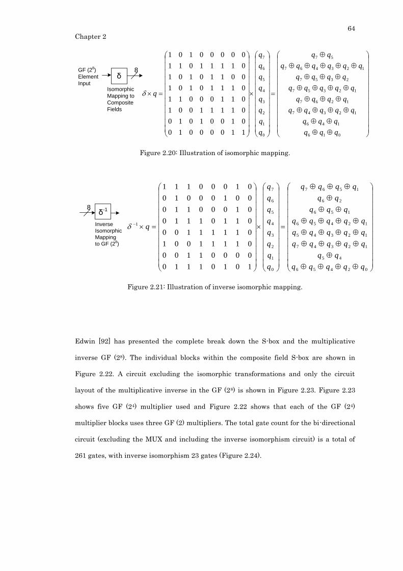
64
Chapter 2
GF (28)
Element
Input
δ
Isomorphic
Mapping to
Composite
Fields
8
016
146
12347
1267
12357
2357
123467
57
0
1
2
3
4
5
6
7
11000010
01001010
01111001
01100011
01110101
00110101
01111011
00000101
qqq
qqq
qqqqq
qqqq
qqqqq
qqqq
qqqqqq
q
q
q
q
q
q
q
q
q
Figure 2.20: Illustration of isomorphic mapping.
02456
45
12347
12345
12456
156
26
1567
0
1
2
3
4
5
6
7
1
10101110
00001100
01111001
01111100
01101110
01000110
00100010
01000111
qqqqq
qqqqq
qqqqq
qqqqq
qqq
qqqq
q
q
q
q
q
q
q
q
qInverse
Isomorphic
Mapping
to GF (28)
δ-18
Figure 2.21: Illustration of inverse isomorphic mapping.
Edwin [92] has presented the complete break down the S-box and the multiplicative
inverse GF (28). The individual blocks within the composite field S-box are shown in
Figure 2.22. A circuit excluding the isomorphic transformations and only the circuit
layout of the multiplicative inverse in the GF (28) is shown in Figure 2.23. Figure 2.23
shows five GF (24) multiplier used and Figure 2.22 shows that each of the GF (24)
multiplier blocks uses three GF (2) multipliers. The total gate count for the bi-directional
circuit (excluding the MUX and including the inverse isomorphism circuit) is a total of
261 gates, with inverse isomorphism 23 gates (Figure 2.24).
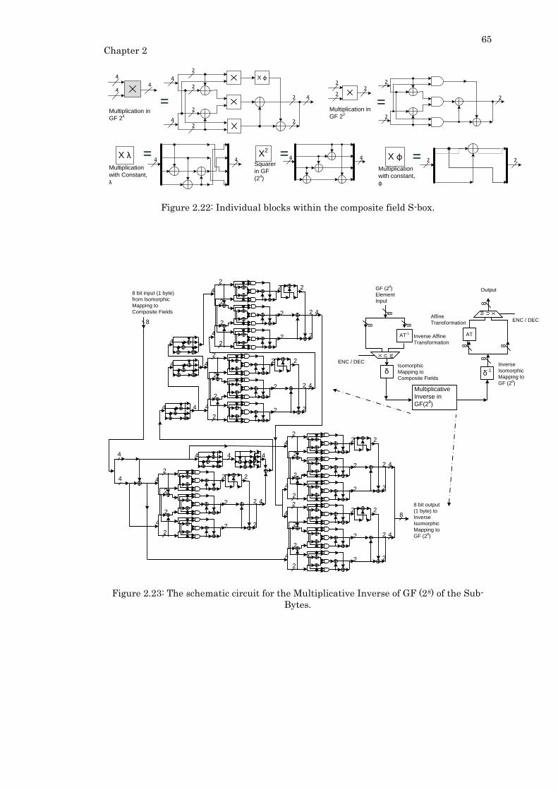
65
Chapter 2
4
4
4
X φ
2
2 4
4
2
2
2
2
4
Multiplication in
GF 24
2
2
2
2
22
Multiplication in
GF 22
Multiplication
with Constant,
λ
X λ4 4
X2
4 4Squarer
in GF
(24)
X φMultiplication
with constant,
φ
2 2
= =
= = =
Figure 2.22: Individual blocks within the composite field S-box.
8 bit input (1 byte)
from Isomorphic
Mapping to
Composite Fields
4
2
2
2
2
42
2
2 42
2
2
4
2
2
2
2
42
2
2 42
2
2
4
2
2
2
2
42
2
2 42
2
2
4
2
2
2
2
42
2
2 42
2
2
4 4
4
4
8
4
2
2
2
2
42
2
2 42
2
2
4 4 44
4
8
8 bit output
(1 byte) to
Inverse
Isomorphic
Mapping to
GF (28)
GF (28)
Element
Input
Multiplicative
Inverse in
GF(28)
δIsomorphic
Mapping to
Composite Fields
Inverse
Isomorphic
Mapping to
GF (28)
δ-1
AT
Affine
Transformation
8
Output
AT-1
Inverse Affine
Transformation
88
8
8 8
8M U X
ENC / DEC
MUX
ENC / DEC
Figure 2.23: The schematic circuit for the Multiplicative Inverse of GF (28) of the Sub-
Bytes.
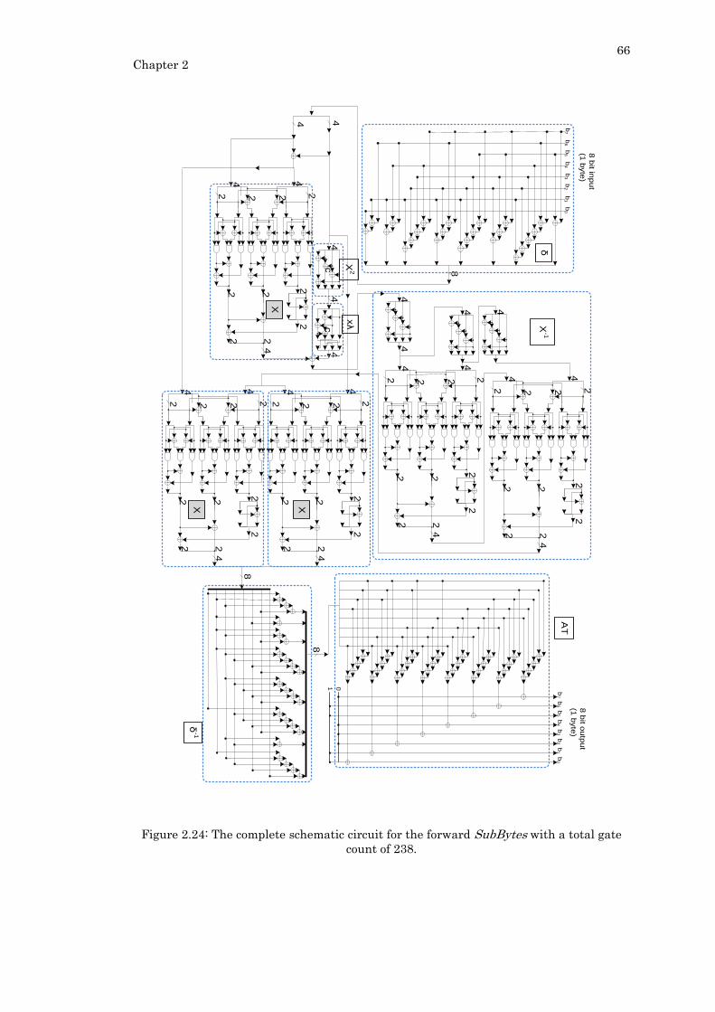
66
Chapter 2
8 b
it inp
ut
(1 b
yte
)
4
2222
42
2 24
22
2
4
2222
42
2 24
22
2
b7
b6
b5
b4
b3
b2
b1
b0
4
2222
42
2 24
22
2
4
2222
42
2 24
22
2
44
4 4
8
4
2222
42
2 24
22
2
44
444
8
8
b0
b1
b2
b3
b4
b5
b6
b7
01
8 b
it ou
tpu
t
(1 b
yte
)
cc
xλ
δ
δ-1
AT
X-1
X
X
X
X2
Figure 2.24: The complete schematic circuit for the forward SubBytes with a total gate
count of 238.
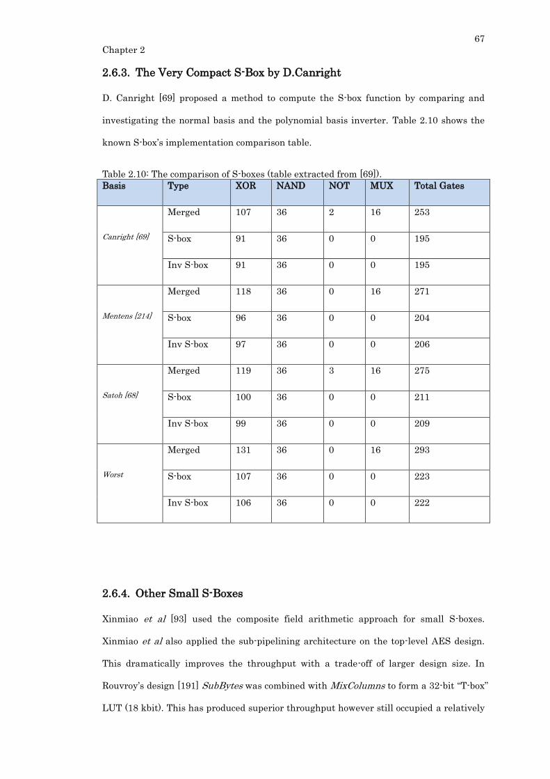
67
Chapter 2
2.6.3. The Very Compact S-Box by D.Canright
D. Canright [69] proposed a method to compute the S-box function by comparing and
investigating the normal basis and the polynomial basis inverter. Table 2.10 shows the
known S-box’s implementation comparison table.
Table 2.10: The comparison of S-boxes (table extracted from [69]).
Basis Type XOR NAND NOT MUX Total Gates
Canright [69]
Merged 107 36 2 16 253
S-box 91 36 0 0 195
Inv S-box 91 36 0 0 195
Mentens [214]
Merged 118 36 0 16 271
S-box 96 36 0 0 204
Inv S-box 97 36 0 0 206
Satoh [68]
Merged 119 36 3 16 275
S-box 100 36 0 0 211
Inv S-box 99 36 0 0 209
Worst
Merged 131 36 0 16 293
S-box 107 36 0 0 223
Inv S-box 106 36 0 0 222
2.6.4. Other Small S-Boxes
Xinmiao et al [93] used the composite field arithmetic approach for small S-boxes.
Xinmiao et al also applied the sub-pipelining architecture on the top-level AES design.
This dramatically improves the throughput with a trade-off of larger design size. In
Rouvroy’s design [191] SubBytes was combined with MixColumns to form a 32-bit “T-box”
LUT (18 kbit). This has produced superior throughput however still occupied a relatively
68
Chapter 2
large area when the size of the LUT was taken into account. For many applications,
throughputs in hundreds of megabits per second would be considered excessive and
therefore, not suitable for resource constrained environment. And another S-box worth
mentioning, is the work proposed by Renfei et al [215]. Renfei et al presented various
critical path delays within the composite field S-box and attempts to minimize the design.
Renfei et al concluded their findings with improved critical path at the expense of a
larger design.
69
Chapter 3
CHAPTER 3
LOW-COMPLEXITY, LOW-AREA FPGA ENCRYPTION
ARCHITECTURE USING A LIGHTWEIGHT CIPHER, THE
SKIPJACK CIPHER
__________________________________________________________________________________
3.1. The Proposed Two Instruction Set Computer (TISC) for
Skipjack Cipher
3.1.1. The Design of the Proposed TISC Architecture
The new proposed architecture aims to create a low-complexity Skipjack cipher processor
using the URISC architecture. The proposed TISC architecture modifies the original
URISC for cryptographic applications. The modifications are: an additional operation
code (opcode) decoder, an XOR block, and a new data path. The original URISC [196] has
a single Adder ALU and processes a single fixed-length instruction. This feature does not
require an opcode field. To define new instruction sets, an opcode decoder circuitry has to
be designed for the architecture.
Skipjack cipher involves the use of bit-wise XOR [63]. Processors in extreme RCEs are
able to compute simple operations such as the XOR [216]. The information given above
and the suitability of Skipjack for low-resource environment [19], the existence of a
dedicated XOR block within the processor is justified. Additionally, with the XOR
operation, the architecture is able to process data movement operations (MOV) with one
less instruction comparing to the URISC’s primitive SBN instruction. The URISC’s SBN
instruction is retained for the conditional instruction branching while the XOR is used
for data memory movement and Skipjack operations. Figure 3.1 depicts the proposed

70
Chapter 3
TISC architecture with the dashed brackets depicting the components added to the
modified URISC.
PC
TISC ALU
PC_WRITE
0
MEMORYMEM_READ
MEM_WRITE
INV
R R_WRITE
N
Z_WRITE
MDR MAR MAR_WRITEMDR_WRITE
MUX0 1 MAR_SEL
MUX0 1PC_OUT_SEL
COMP_SEL
Adder XOR
Z
CIN
N_WRITE[9]OP
MUX0 1
OP_SEL
0
OP_WRITE
0 1MUX
MUX0 1
Figure 3.1: The illustration of the TISC data-path architecture3.
3.1.2. Developing the Modified SBN URISC for the Proposed TISC
Architecture
A processor has to have basic operations in order to perform computing tasks. Basic
operations such as data movement, copying, deletion, instruction jumping and No
Operation (NOP) are required. Gilreath and Laplante [54], stated and proved that the
3 Published in: Kong Jia Hao, Ang Li-Minn, Seng Kah Phooi, Ong Fong Tien, “Low-complexity Two
Instruction Set Computer architecture for sensor network using Skipjack encryption”,
Proceedings of the 25th of the International Conference on Information Networking (ICOIN
2011), pp. 472-477, ISBN: 978-1-61284-661-3, 2011, Figure 3.
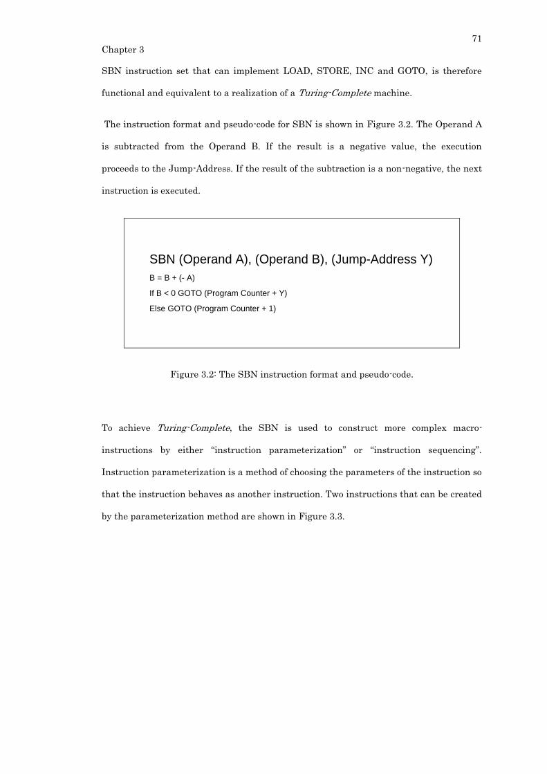
71
Chapter 3
SBN instruction set that can implement LOAD, STORE, INC and GOTO, is therefore
functional and equivalent to a realization of a Turing-Complete machine.
The instruction format and pseudo-code for SBN is shown in Figure 3.2. The Operand A
is subtracted from the Operand B. If the result is a negative value, the execution
proceeds to the Jump-Address. If the result of the subtraction is a non-negative, the next
instruction is executed.
SBN (Operand A), (Operand B), (Jump-Address Y)
B = B + (- A)
If B < 0 GOTO (Program Counter + Y)
Else GOTO (Program Counter + 1)
Figure 3.2: The SBN instruction format and pseudo-code.
To achieve Turing-Complete, the SBN is used to construct more complex macro-
instructions by either “instruction parameterization” or “instruction sequencing”.
Instruction parameterization is a method of choosing the parameters of the instruction so
that the instruction behaves as another instruction. Two instructions that can be created
by the parameterization method are shown in Figure 3.3.
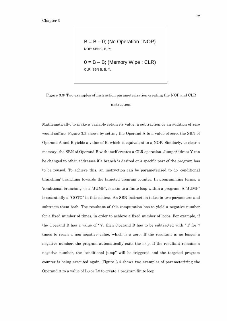
72
Chapter 3
B = B – 0; (No Operation : NOP)
NOP: SBN 0, B, Y;
0 = B – B; (Memory Wipe : CLR)
CLR: SBN B, B, Y;
;
Figure 3.3: Two examples of instruction parameterization creating the NOP and CLR
instruction.
Mathematically, to make a variable retain its value, a subtraction or an addition of zero
would suffice. Figure 3.3 shows by setting the Operand A to a value of zero, the SBN of
Operand A and B yields a value of B, which is equivalent to a NOP. Similarly, to clear a
memory, the SBN of Operand B with itself creates a CLR operation. Jump-Address Y can
be changed to other addresses if a branch is desired or a specific part of the program has
to be reused. To achieve this, an instruction can be parameterized to do ‘conditional
branching’ branching towards the targeted program counter. In programming terms, a
‘conditional branching’ or a “JUMP”, is akin to a finite loop within a program. A “JUMP”
is essentially a “GOTO” in this context. An SBN instruction takes in two parameters and
subtracts them both. The resultant of this computation has to yield a negative number
for a fixed number of times, in order to achieve a fixed number of loops. For example, if
the Operand B has a value of ‘-7’, then Operand B has to be subtracted with ‘-1’ for 7
times to reach a non-negative value, which is a zero. If the resultant is no longer a
negative number, the program automatically exits the loop. If the resultant remains a
negative number, the ‘conditional jump” will be triggered and the targeted program
counter is being executed again. Figure 3.4 shows two examples of parameterizing the
Operand A to a value of L3 or L8 to create a program finite loop.
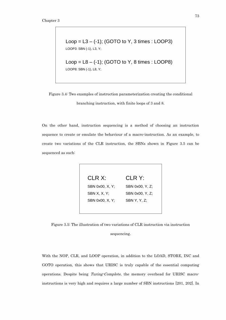
73
Chapter 3
Loop = L3 – (-1); (GOTO to Y, 3 times : LOOP3)
LOOP3: SBN (-1), L3, Y;
Loop = L8 – (-1); (GOTO to Y, 8 times : LOOP8)
LOOP8: SBN (-1), L8, Y;
Figure 3.4: Two examples of instruction parameterization creating the conditional
branching instruction, with finite loops of 3 and 8.
On the other hand, instruction sequencing is a method of choosing an instruction
sequence to create or emulate the behaviour of a macro-instruction. As an example, to
create two variations of the CLR instruction, the SBNs shown in Figure 3.5 can be
sequenced as such:
CLR X:
SBN 0x00, X, Y;
SBN X, X, Y;
SBN 0x00, X, Y;
CLR Y:
SBN 0x00, Y, Z;
SBN 0x00, Y, Z;
SBN Y, Y, Z;
Figure 3.5: The illustration of two variations of CLR instruction via instruction
sequencing.
With the NOP, CLR, and LOOP operation, in addition to the LOAD, STORE, INC and
GOTO operation, this shows that URISC is truly capable of the essential computing
operations. Despite being Turing-Complete, the memory overhead for URISC macro-
instructions is very high and requires a large number of SBN instructions [201, 202]. In
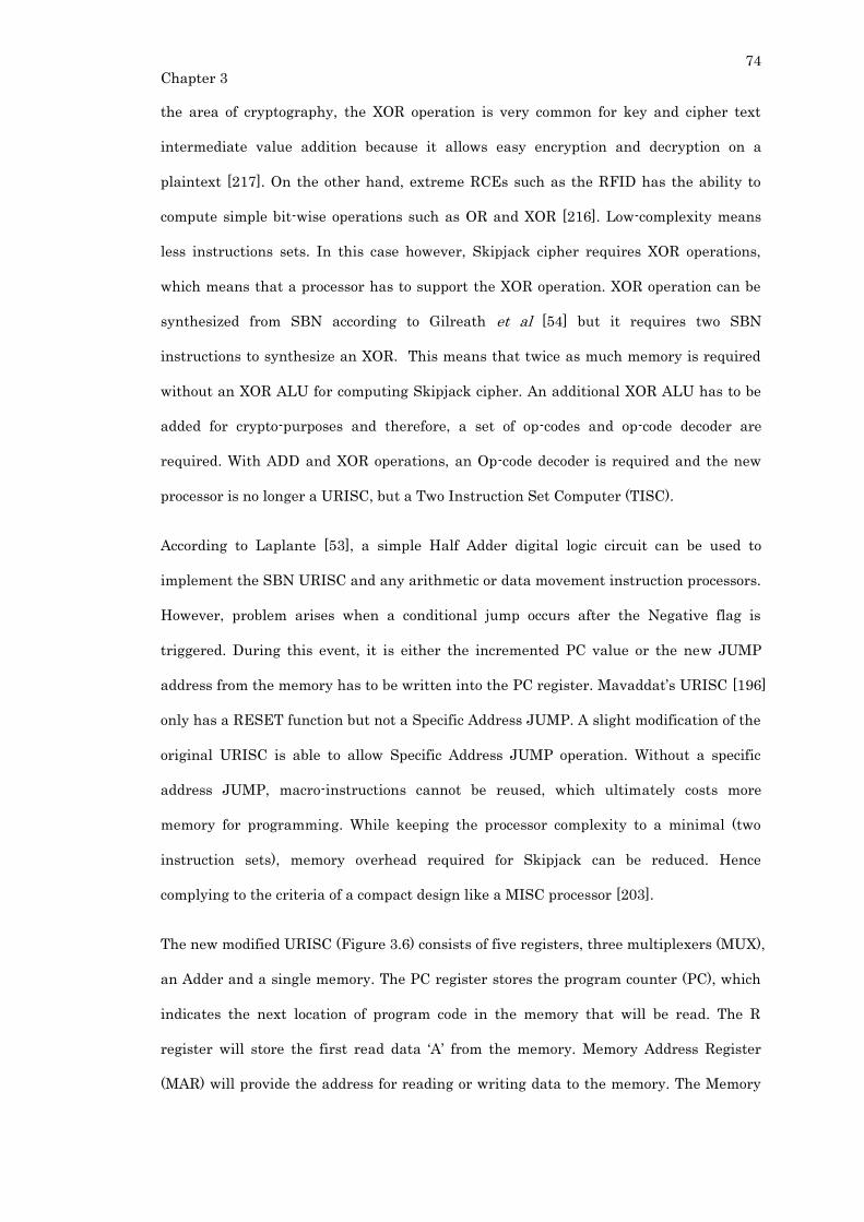
74
Chapter 3
the area of cryptography, the XOR operation is very common for key and cipher text
intermediate value addition because it allows easy encryption and decryption on a
plaintext [217]. On the other hand, extreme RCEs such as the RFID has the ability to
compute simple bit-wise operations such as OR and XOR [216]. Low-complexity means
less instructions sets. In this case however, Skipjack cipher requires XOR operations,
which means that a processor has to support the XOR operation. XOR operation can be
synthesized from SBN according to Gilreath et al [54] but it requires two SBN
instructions to synthesize an XOR. This means that twice as much memory is required
without an XOR ALU for computing Skipjack cipher. An additional XOR ALU has to be
added for crypto-purposes and therefore, a set of op-codes and op-code decoder are
required. With ADD and XOR operations, an Op-code decoder is required and the new
processor is no longer a URISC, but a Two Instruction Set Computer (TISC).
According to Laplante [53], a simple Half Adder digital logic circuit can be used to
implement the SBN URISC and any arithmetic or data movement instruction processors.
However, problem arises when a conditional jump occurs after the Negative flag is
triggered. During this event, it is either the incremented PC value or the new JUMP
address from the memory has to be written into the PC register. Mavaddat’s URISC [196]
only has a RESET function but not a Specific Address JUMP. A slight modification of the
original URISC is able to allow Specific Address JUMP operation. Without a specific
address JUMP, macro-instructions cannot be reused, which ultimately costs more
memory for programming. While keeping the processor complexity to a minimal (two
instruction sets), memory overhead required for Skipjack can be reduced. Hence
complying to the criteria of a compact design like a MISC processor [203].
The new modified URISC (Figure 3.6) consists of five registers, three multiplexers (MUX),
an Adder and a single memory. The PC register stores the program counter (PC), which
indicates the next location of program code in the memory that will be read. The R
register will store the first read data ‘A’ from the memory. Memory Address Register
(MAR) will provide the address for reading or writing data to the memory. The Memory
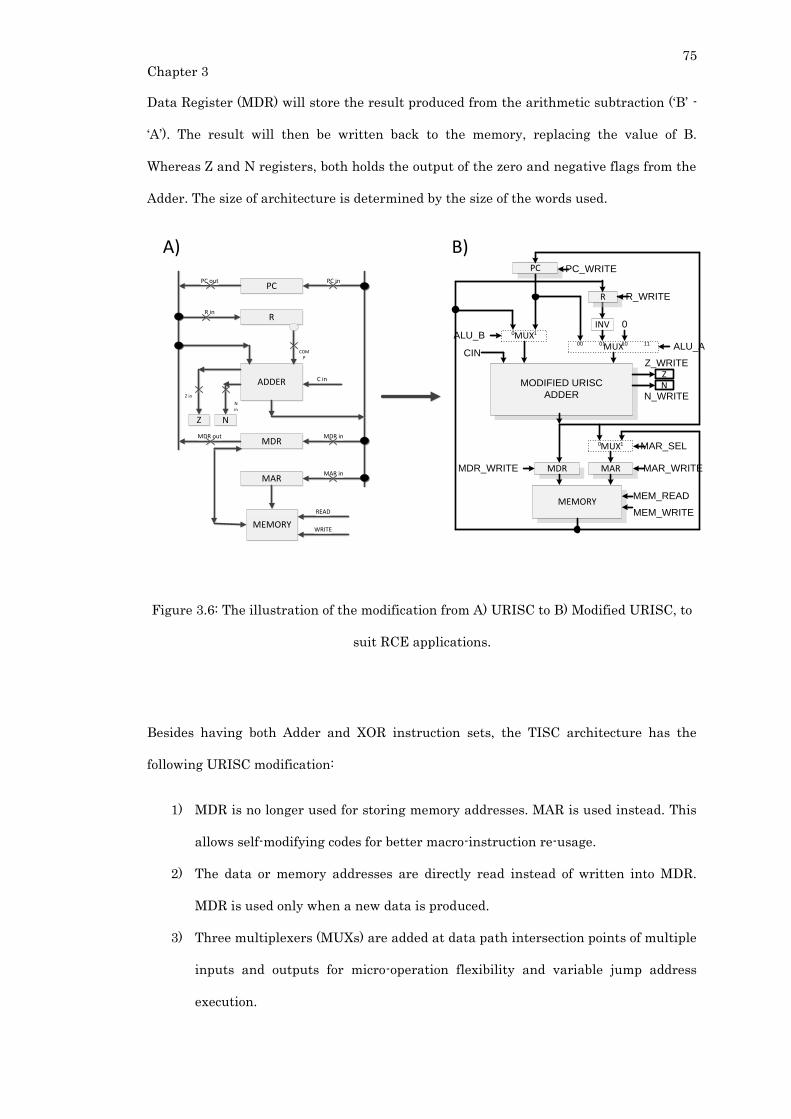
75
Chapter 3
Data Register (MDR) will store the result produced from the arithmetic subtraction (‘B’ -
‘A’). The result will then be written back to the memory, replacing the value of B.
Whereas Z and N registers, both holds the output of the zero and negative flags from the
Adder. The size of architecture is determined by the size of the words used.
ADDER
PC
Z N
R
MDR
MAR
PC out PC in
R in
Z in
N in
MDR out MDR in
MAR in
C in
MEMORY
READ
WRITE
COMP
A) B)PC
MODIFIED URISC
ADDER
PC_WRITE
0
MEMORYMEM_READ
MEM_WRITE
INV
R R_WRITE
N
Z_WRITE
MDR MAR MAR_WRITEMDR_WRITE
MUX0 1 MAR_SEL
MUX0 1ALU_BALU_A
Z
CIN
N_WRITE
MUX00 01 10 11
Figure 3.6: The illustration of the modification from A) URISC to B) Modified URISC, to
suit RCE applications.
Besides having both Adder and XOR instruction sets, the TISC architecture has the
following URISC modification:
1) MDR is no longer used for storing memory addresses. MAR is used instead. This
allows self-modifying codes for better macro-instruction re-usage.
2) The data or memory addresses are directly read instead of written into MDR.
MDR is used only when a new data is produced.
3) Three multiplexers (MUXs) are added at data path intersection points of multiple
inputs and outputs for micro-operation flexibility and variable jump address
execution.
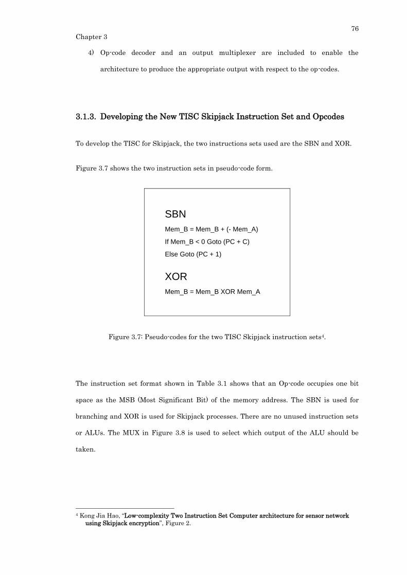
76
Chapter 3
4) Op-code decoder and an output multiplexer are included to enable the
architecture to produce the appropriate output with respect to the op-codes.
3.1.3. Developing the New TISC Skipjack Instruction Set and Opcodes
To develop the TISC for Skipjack, the two instructions sets used are the SBN and XOR.
Figure 3.7 shows the two instruction sets in pseudo-code form.
SBN
Mem_B = Mem_B + (- Mem_A)
If Mem_B < 0 Goto (PC + C)
Else Goto (PC + 1)
XOR
Mem_B = Mem_B XOR Mem_A
Figure 3.7: Pseudo-codes for the two TISC Skipjack instruction sets4.
The instruction set format shown in Table 3.1 shows that an Op-code occupies one bit
space as the MSB (Most Significant Bit) of the memory address. The SBN is used for
branching and XOR is used for Skipjack processes. There are no unused instruction sets
or ALUs. The MUX in Figure 3.8 is used to select which output of the ALU should be
taken.
4 Kong Jia Hao, “Low-complexity Two Instruction Set Computer architecture for sensor network
using Skipjack encryption”, Figure 2.
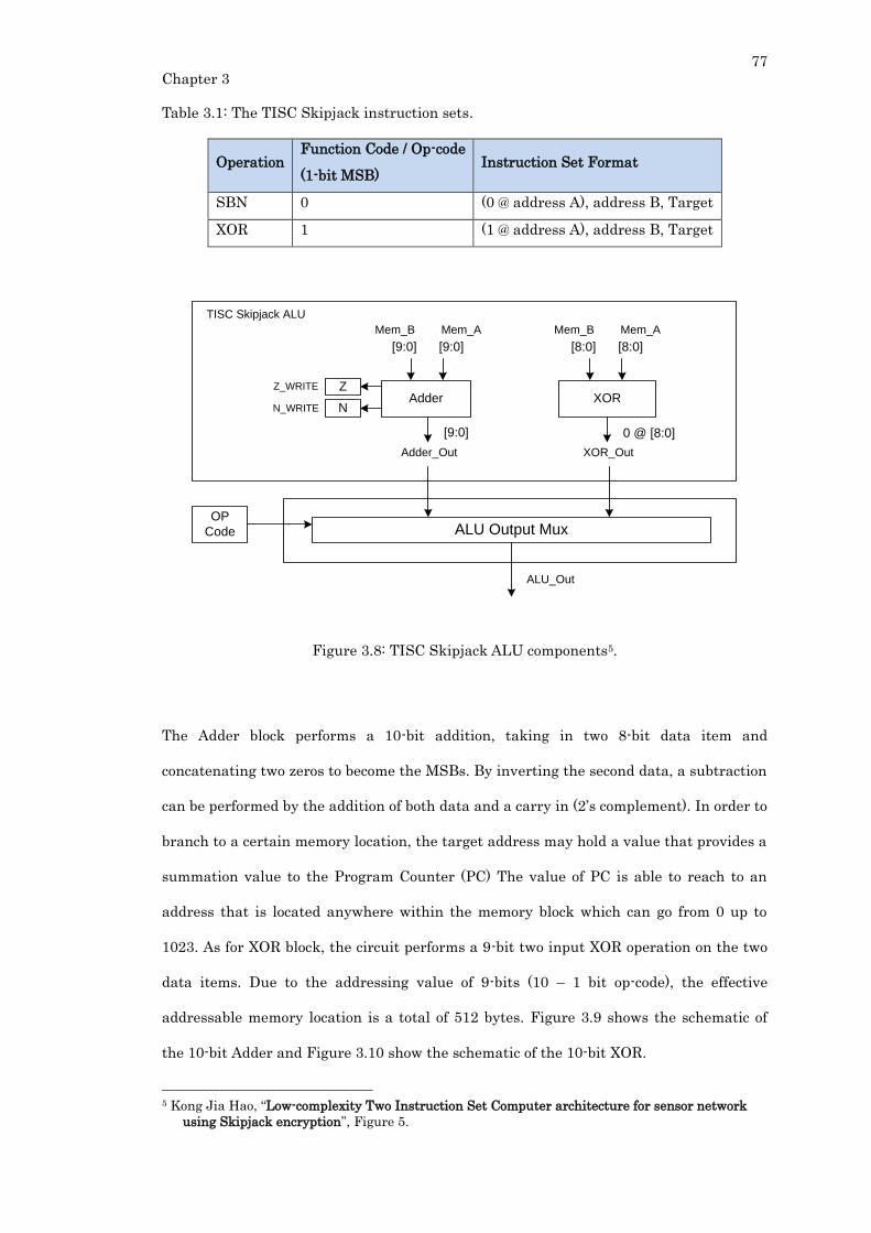
77
Chapter 3
Table 3.1: The TISC Skipjack instruction sets.
Operation Function Code / Op-code
(1-bit MSB) Instruction Set Format
SBN 0 (0 @ address A), address B, Target
XOR 1 (1 @ address A), address B, Target
N
Z_WRITE Z
N_WRITEXOR
[8:0] [8:0]
0 @ [8:0]
Mem_B Mem_A
XOR_Out
Adder
[9:0] [9:0]
[9:0]
Mem_B Mem_A
Adder_Out
OP
Code ALU Output Mux
ALU_Out
TISC Skipjack ALU
Figure 3.8: TISC Skipjack ALU components5.
The Adder block performs a 10-bit addition, taking in two 8-bit data item and
concatenating two zeros to become the MSBs. By inverting the second data, a subtraction
can be performed by the addition of both data and a carry in (2’s complement). In order to
branch to a certain memory location, the target address may hold a value that provides a
summation value to the Program Counter (PC) The value of PC is able to reach to an
address that is located anywhere within the memory block which can go from 0 up to
1023. As for XOR block, the circuit performs a 9-bit two input XOR operation on the two
data items. Due to the addressing value of 9-bits (10 – 1 bit op-code), the effective
addressable memory location is a total of 512 bytes. Figure 3.9 shows the schematic of
the 10-bit Adder and Figure 3.10 show the schematic of the 10-bit XOR.
5 Kong Jia Hao, “Low-complexity Two Instruction Set Computer architecture for sensor network
using Skipjack encryption”, Figure 5.
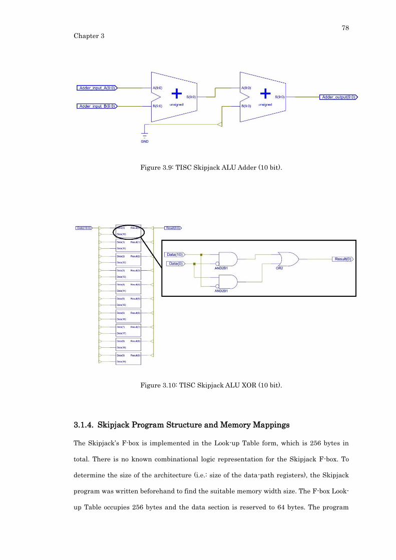
78
Chapter 3
Figure 3.9: TISC Skipjack ALU Adder (10 bit).
Figure 3.10: TISC Skipjack ALU XOR (10 bit).
3.1.4. Skipjack Program Structure and Memory Mappings
The Skipjack’s F-box is implemented in the Look-up Table form, which is 256 bytes in
total. There is no known combinational logic representation for the Skipjack F-box. To
determine the size of the architecture (i.e.: size of the data-path registers), the Skipjack
program was written beforehand to find the suitable memory width size. The F-box Look-
up Table occupies 256 bytes and the data section is reserved to 64 bytes. The program
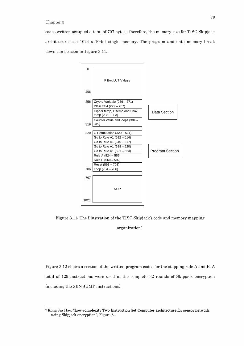
79
Chapter 3
codes written occupied a total of 707 bytes. Therefore, the memory size for TISC Skipjack
architecture is a 1024 x 10-bit single memory. The program and data memory break
down can be seen in Figure 3.11.
Figure 3.11: The illustration of the TISC Skipjack’s code and memory mapping
organization6.
Figure 3.12 shows a section of the written program codes for the stepping rule A and B. A
total of 129 instructions were used in the complete 32 rounds of Skipjack encryption
(including the SBN JUMP instructions).
6 Kong Jia Hao, “Low-complexity Two Instruction Set Computer architecture for sensor network
using Skipjack encryption”, Figure 8.
Data Section
Program Section
256
319
Plain Text (272 – 287)
Crypto Variable (256 – 271)
Cipher temp, G temp and Fbox
temp (288 – 303)
Counter value and loops (304 –
319)
Go to Rule A1 (512 – 514)
Rule A (524 – 559)
G Permutation (320 – 511)
Go to Rule A1 (515 – 517)
Go to Rule A1 (518 – 520)
Go to Rule A1 (521 – 523)
Rule B (560 – 592)
Reset (593 – 703)
706
320
Loop (704 – 706)
F Box LUT Values
0
255
NOP
707
1023
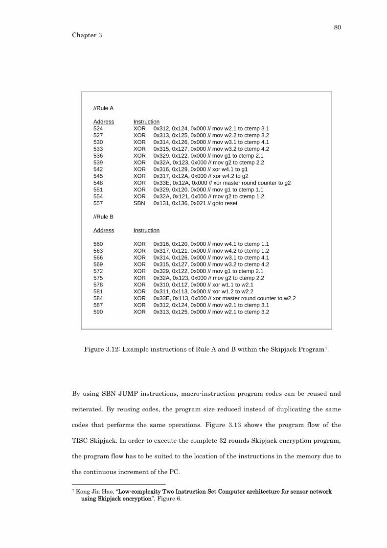
80
Chapter 3
//Rule A
Address Instruction
524 XOR 0x312, 0x124, 0x000 // mov w2.1 to ctemp 3.1
527 XOR 0x313, 0x125, 0x000 // mov w2.2 to ctemp 3.2
530 XOR 0x314, 0x126, 0x000 // mov w3.1 to ctemp 4.1
533 XOR 0x315, 0x127, 0x000 // mov w3.2 to ctemp 4.2
536 XOR 0x329, 0x122, 0x000 // mov g1 to ctemp 2.1
539 XOR 0x32A, 0x123, 0x000 // mov g2 to ctemp 2.2
542 XOR 0x316, 0x129, 0x000 // xor w4.1 to g1
545 XOR 0x317, 0x12A, 0x000 // xor w4.2 to g2
548 XOR 0x33E, 0x12A, 0x000 // xor master round counter to g2
551 XOR 0x329, 0x120, 0x000 // mov g1 to ctemp 1.1
554 XOR 0x32A, 0x121, 0x000 // mov g2 to ctemp 1.2
557 SBN 0x131, 0x136, 0x021 // goto reset
//Rule B
Address Instruction
560 XOR 0x316, 0x120, 0x000 // mov w4.1 to ctemp 1.1
563 XOR 0x317, 0x121, 0x000 // mov w4.2 to ctemp 1.2
566 XOR 0x314, 0x126, 0x000 // mov w3.1 to ctemp 4.1
569 XOR 0x315, 0x127, 0x000 // mov w3.2 to ctemp 4.2
572 XOR 0x329, 0x122, 0x000 // mov g1 to ctemp 2.1
575 XOR 0x32A, 0x123, 0x000 // mov g2 to ctemp 2.2
578 XOR 0x310, 0x112, 0x000 // xor w1.1 to w2.1
581 XOR 0x311, 0x113, 0x000 // xor w1.2 to w2.2
584 XOR 0x33E, 0x113, 0x000 // xor master round counter to w2.2
587 XOR 0x312, 0x124, 0x000 // mov w2.1 to ctemp 3.1
590 XOR 0x313, 0x125, 0x000 // mov w2.1 to ctemp 3.2
Figure 3.12: Example instructions of Rule A and B within the Skipjack Program7.
By using SBN JUMP instructions, macro-instruction program codes can be reused and
reiterated. By reusing codes, the program size reduced instead of duplicating the same
codes that performs the same operations. Figure 3.13 shows the program flow of the
TISC Skipjack. In order to execute the complete 32 rounds Skipjack encryption program,
the program flow has to be suited to the location of the instructions in the memory due to
the continuous increment of the PC.
7 Kong Jia Hao, “Low-complexity Two Instruction Set Computer architecture for sensor network
using Skipjack encryption”, Figure 6.
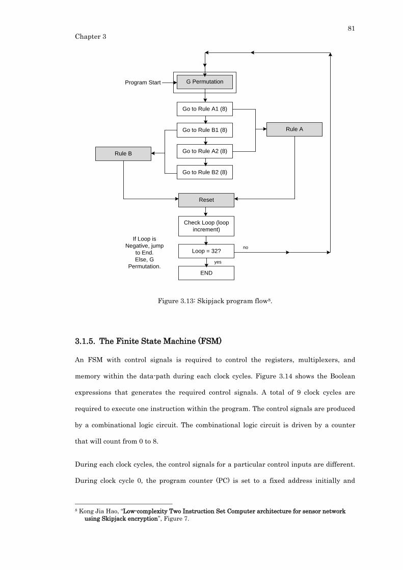
81
Chapter 3
Rule A
Rule B
Reset
Loop = 32?
If Loop is
Negative, jump
to End.
Else, G
Permutation.
G Permutation
Go to Rule A1 (8)
END
Program Start
Go to Rule B1 (8)
Go to Rule A2 (8)
Go to Rule B2 (8)
Check Loop (loop
increment)
yes
no
Figure 3.13: Skipjack program flow8.
3.1.5. The Finite State Machine (FSM)
An FSM with control signals is required to control the registers, multiplexers, and
memory within the data-path during each clock cycles. Figure 3.14 shows the Boolean
expressions that generates the required control signals. A total of 9 clock cycles are
required to execute one instruction within the program. The control signals are produced
by a combinational logic circuit. The combinational logic circuit is driven by a counter
that will count from 0 to 8.
During each clock cycles, the control signals for a particular control inputs are different.
During clock cycle 0, the program counter (PC) is set to a fixed address initially and
8 Kong Jia Hao, “Low-complexity Two Instruction Set Computer architecture for sensor network
using Skipjack encryption”, Figure 7.

82
Chapter 3
loaded into the memory address register (MAR). The zero register (Z) will be set by the
adder’s output to determine whether the PC has restarted to 0x00. Using this initial PC
value, a set of memory value is read and written to the MAR. Now, the current MAR
value holds the memory location of the first operand (A). Next, the PC value is then
increased by 1 in order to access the address of the second operand (B). At clock cycle 2,
the value of A is then read and then store to R register temporary.
During clock cycle 3, the current PC+1 value is loaded into MAR. During clock cycle 4,
the memory location of the second operand B is then read and store back to MAR again.
The PC value is also increased by 1 during the same clock cycle. At the clock cycle 6, the
value of B, which will be used in arithmetic operation, is read. The adder perform the
arithmetic operation (B-A). The N register is used to determine whether the result or the
arithmetic calculation is negative via a negative flag to. During the same clock cycle, the
PC value is again increased by 1 (which is now PC+2) which will locate the jump
program memory address for the next clock cycle.
After the TISC arithmetic operations are performed, clock cycle 7 will load the jump
address from memory. The jump address will then be added into the PC value during the
same clock cycle. The jump address value will only be added to the PC value, provided
that the arithmetic (B-A) produced negative result (subtract and branch if negative). The
last clock cycle 8 will have the PC value increased by 1 again and thus, a single TISC
instruction (regardless of which instructions) completed.
Equations (1) to (14) shown in Figure 3.15 are the Boolean expressions for each control
signals generated via a 4-bit counter. As for the PC_WRITE control signal, the N
register’s value affects to whether the architecture decides to branch or not. During the
7th clock cycle, PC_WRITE will be 1 if the arithmetic summation of the adder, (B-A),
produced negative result. This enables the jump address for that instruction to be added
into the PC register and thus, resulting to a branch. If the N register is 0, there would
not be any branching off to another program location. The PC register would continue to
increase by 1. Then, the following instruction in the written program code will be
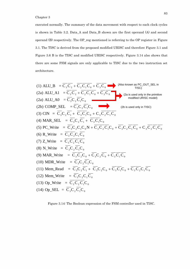
83
Chapter 3
executed normally. The summary of the data movement with respect to each clock cycles
is shown in Table 3.2. Data_A and Data_B shown are the first operand (A) and second
operand (B) respectively. The OP_reg mentioned is referring to the OP register in Figure
3.1. The TISC is derived from the proposed modified URISC and therefore Figure 3.1 and
Figure 3.6 B is the TISC and modified URISC respectively. Figure 3.14 also shows that
there are some FSM signals are only applicable to TISC due to the two instruction set
architecture.
0123
0123
0123
0123013023123
0123
013023023
0123
0123
0123
0123012301230123
013123
0123013123
0123
0123
0301223
0301223
CCCC = Op_SEL (14)
CCCC = Op_Write (13)
CCCC = Mem_Write (12)
CCCC CCC CCC CCC = Mem_Read (11)
CCCC = MDR_Write (10)
CCC CCC CCC = MAR_Write (9)
CCCC = N_Write (8)
CCCC = Z_Write(7)
CCCC = R_Write (6)
CCCC CCCC CCCC NCCCC = PC_Write (5)
CCC CCC = MAR_SEL (4)
CCCC CCC CCC = CIN (3)
CCCC = COMP_SEL (2b)
CCCC = ALU_A0 (2a)
CCCCCCC = ALU_A1 (2a)
CCCCCCC = ALU_B (1)
(Also known as PC_OUT_SEL in
TISC)
(2b is used only in TISC)
(2a is used only in the primitive
modified URISC model)
Figure 3.14: The Boolean expression of the FSM controller used in TISC.
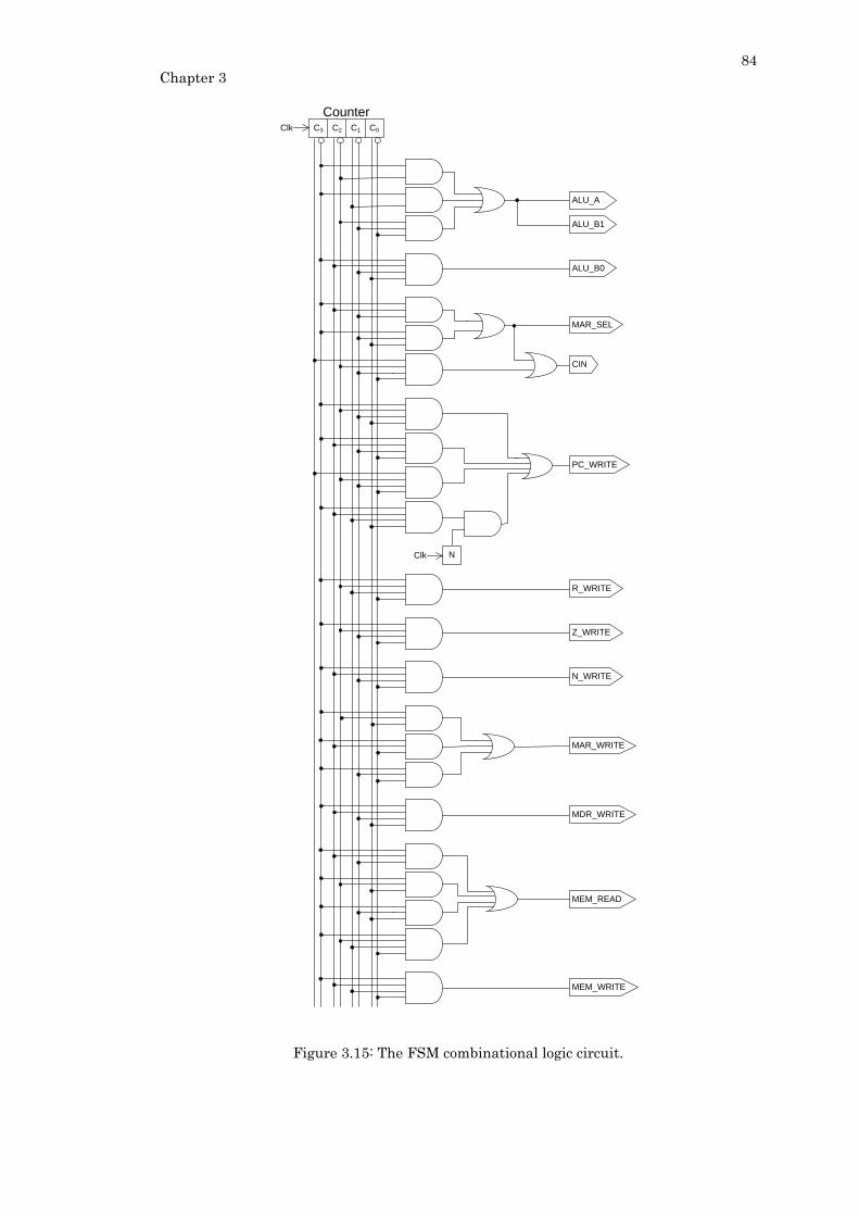
84
Chapter 3
C3 C2 C1 C0
Counter
ALU_A
ALU_B1
ALU_B0
CIN
MAR_SEL
Clk
PC_WRITE
NClk
R_WRITE
Z_WRITE
N_WRITE
MAR_WRITE
MDR_WRITE
MEM_WRITE
MEM_READ
Figure 3.15: The FSM combinational logic circuit.

85
Chapter 3
Table 3.2: The summary of the data movement with respect to each clock cycles of the
TISC architecture.
Clock
Cycle
Data_A Data_B Additional Remarks FSM Signals
0 Address of
Data_A is
loaded into
MAR.
- (PC) to MAR. Z_WRITE,
MAR_WRITE
1 Data_A is
loaded to
R_reg
- Opcode (if available) from the
instruction to OP code
register.
PC_OUT_SEL,
MAR_WRITE,
MEM_READ,
OP_WRITE,
MAR_SEL
2 - Address of
Data_B is
loaded into
MAR.
(PC + 1) to MAR R_WRITE,
C_IN,
PC_OUT_SEL,
MEM_READ
3 - Data_B is
loaded out
- C_IN,
PC_WRITE,
MAR_WRITE
4 Data_A is
read from
R_reg
Data_B is
read from
memory
directly
The output of the arithmetic
calculation for both Data_A
and Data_B is selected via
MUX
PC_OUT_SEL,
MAR_WRITE,
MEM_READ,
MAR_SEL
5 - - The computed data is stored
in MDR
C_IN,
N_WRITE,
PC_OUT_SEL,
MDR_WRITE,
MEM_READ
6 - - PC + 2 to MAR C_IN,
PC_WRITE,
MAR_WRITE,
MEM_WRITE
7 - - Branch code loaded. If -ve
branch occurs, PC + 2 +
'branch_address' is the new
PC value.
PC_OUT_SEL,
PC_WRITE,
MEM_READ
8 - - PC + 3 (instruction cycles
reset)
C_IN,
PC_WRITE
3.1.6. The Memory Readdressing Modes (Programmable Addresses and
Self-Modifying Codes)
In URISC programming, there is a unique way of coding that allows the code itself to
‘self-modify’. This is a very unique feature in instruction set programming and is used
very frequently in the proposed architecture and therefore, the intricate details of the
applied self-modifying code techniques have to be explained. Self-modifying code is code

86
Chapter 3
that alters its own instruction in the process of execution. This method is usually used to
improve the codes’ performance or to simply reduce repetitively similar code and helps
reducing memory usage. Reducing memory usage is crucial towards designing a
minimalistic TISC. This term is usually applied to code where the self-modification is
intentional, not in situations where the code accidentally modifies itself due to
programming error.
In URISC programming, if the architecture is in 8-bits, then the self-modifying addresses
are a total of 256 addresses, provided that there is no op-code to be filtered via the MAR.
Presumably is an op-code is forced upon the URISC. This would make the 8-bit
architecture to be a 7-bit architecture because 1 MSB would have to be occupied for op-
code. On top of that, an op-code decoder would have to present. This would the effective
word width to 7-bit. A 7-bit architecture will provide 2 ^ 7 addressing spaces. For
example, 27 = 128 addresses. This would mean that there will be only 128 memory
addresses available for programming. Note that each SBN instructions consist of 3 words,
meaning 3 memory locations will be occupied for a single SBN instruction. To identify
the programmable memory section, the 1-bit op-code has to be accounted for. So, the
programmable address for an 8-bit architecture and a 1-bit op-code is 7-bits address,
meaning there are 128 addresses that are capable of ‘self-modifying’. The addressable
memories and the self-modifying code are mentioned here because they play an
important role in making URISC programming capable of complex operations which is
used in this work presented in the latter chapters.
Figure 3.16 illustrates the visual explanation of the self-modifying addresses. The
question may arise that, why a ‘0’ is concatenated as an MSB? This is because when a
single bit op-code exists, that op-code that to be taken out and decoded via op-code
decoder circuitry. Once the op-code is taken out of the 8-bit address, the 1-bit space has
to be filled. So, a ‘0’ is concatenated and this indirectly alters the value of the address. In
other words, this ‘new’ address is still the same address if it were to be view as a 7-bit
address, no change to that. If the address were viewed as an 8-bit address, the address is
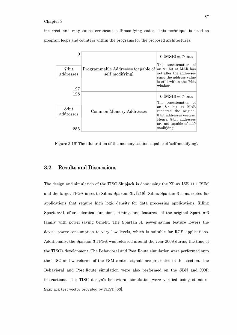
87
Chapter 3
incorrect and may cause erroneous self-modifying codes. This technique is used to
program loops and counters within the programs for the proposed architectures.
Programmable Addresses (capable of
self-modifying)
Common Memory Addresses
0 (MSB) @ 7-bits
127
128
255
0
7-bit
addresses
8-bit
addresses
0 (MSB) @ 7-bits
The concatenation of
an 8th bit at MAR
rendered the original
8-bit addresses useless.
Hence, 8-bit addresses
are not capable of self-
modifying.
The concatenation of
an 8th bit at MAR has
not alter the addresses
since the address value
is still within the 7-bit
window.
Figure 3.16: The illustration of the memory section capable of ‘self-modifying’.
3.2. Results and Discussions
The design and simulation of the TISC Skipjack is done using the Xilinx ISE 11.1 ISIM
and the target FPGA is set to Xilinx Spartan-3L [218]. Xilinx Spartan-3 is marketed for
applications that require high logic density for data processing applications. Xilinx
Spartan-3L offers identical functions, timing, and features of the original Spartan-3
family with power-saving benefit. The Spartan-3L power-saving feature lowers the
device power consumption to very low levels, which is suitable for RCE applications.
Additionally, the Spartan-3 FPGA was released around the year 2008 during the time of
the TISC’s development. The Behavioral and Post-Route simulation were performed onto
the TISC and waveforms of the FSM control signals are presented in this section. The
Behavioral and Post-Route simulation were also performed on the SBN and XOR
instructions. The TISC design’s behavioral simulation were verified using standard
Skipjack test vector provided by NIST [63].
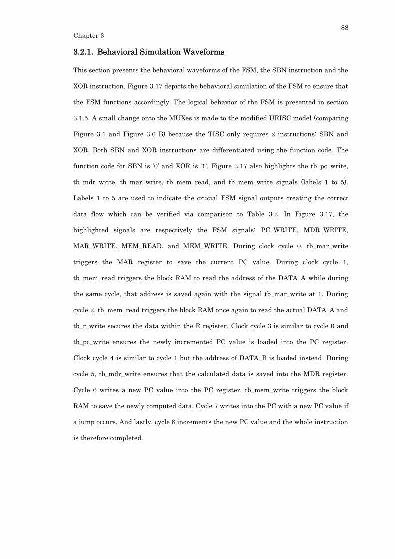
88
Chapter 3
3.2.1. Behavioral Simulation Waveforms
This section presents the behavioral waveforms of the FSM, the SBN instruction and the
XOR instruction. Figure 3.17 depicts the behavioral simulation of the FSM to ensure that
the FSM functions accordingly. The logical behavior of the FSM is presented in section
3.1.5. A small change onto the MUXes is made to the modified URISC model (comparing
Figure 3.1 and Figure 3.6 B) because the TISC only requires 2 instructions: SBN and
XOR. Both SBN and XOR instructions are differentiated using the function code. The
function code for SBN is ‘0’ and XOR is ‘1’. Figure 3.17 also highlights the tb_pc_write,
tb_mdr_write, tb_mar_write, tb_mem_read, and tb_mem_write signals (labels 1 to 5).
Labels 1 to 5 are used to indicate the crucial FSM signal outputs creating the correct
data flow which can be verified via comparison to Table 3.2. In Figure 3.17, the
highlighted signals are respectively the FSM signals: PC_WRITE, MDR_WRITE,
MAR_WRITE, MEM_READ, and MEM_WRITE. During clock cycle 0, tb_mar_write
triggers the MAR register to save the current PC value. During clock cycle 1,
tb_mem_read triggers the block RAM to read the address of the DATA_A while during
the same cycle, that address is saved again with the signal tb_mar_write at 1. During
cycle 2, tb_mem_read triggers the block RAM once again to read the actual DATA_A and
tb_r_write secures the data within the R register. Clock cycle 3 is similar to cycle 0 and
tb_pc_write ensures the newly incremented PC value is loaded into the PC register.
Clock cycle 4 is similar to cycle 1 but the address of DATA_B is loaded instead. During
cycle 5, tb_mdr_write ensures that the calculated data is saved into the MDR register.
Cycle 6 writes a new PC value into the PC register, tb_mem_write triggers the block
RAM to save the newly computed data. Cycle 7 writes into the PC with a new PC value if
a jump occurs. And lastly, cycle 8 increments the new PC value and the whole instruction
is therefore completed.
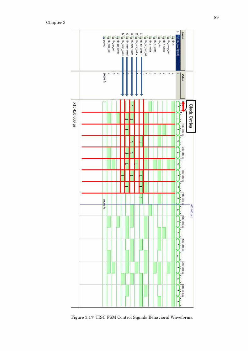
89
Chapter 3
Figure 3.17: TISC FSM Control Signals Behavioral Waveforms.
Clo
ck C
ycle
s
1
1
1
1
1
1
1
1
1
1
1
1
2
3
1
1
1
4
5
1
1
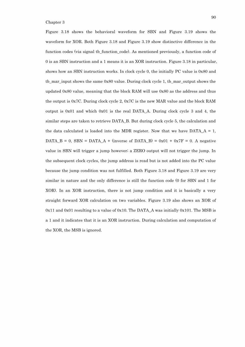
90
Chapter 3
Figure 3.18 shows the behavioral waveform for SBN and Figure 3.19 shows the
waveform for XOR. Both Figure 3.18 and Figure 3.19 show distinctive difference in the
function codes (via signal tb_function_code). As mentioned previously, a function code of
0 is an SBN instruction and a 1 means it is an XOR instruction. Figure 3.18 in particular,
shows how an SBN instruction works. In clock cycle 0, the initially PC value is 0x80 and
tb_mar_input shows the same 0x80 value. During clock cycle 1, tb_mar_output shows the
updated 0x80 value, meaning that the block RAM will use 0x80 as the address and thus
the output is 0x7C. During clock cycle 2, 0x7C is the new MAR value and the block RAM
output is 0x01 and which 0x01 is the real DATA_A. During clock cycle 3 and 4, the
similar steps are taken to retrieve DATA_B. But during clock cycle 5, the calculation and
the data calculated is loaded into the MDR register. Now that we have DATA_A = 1,
DATA_B = 0, SBN = DATA_A + (inverse of DATA_B) = 0x01 + 0x7F = 0. A negative
value in SBN will trigger a jump however; a ZERO output will not trigger the jump. In
the subsequent clock cycles, the jump address is read but is not added into the PC value
because the jump condition was not fulfilled. Both Figure 3.18 and Figure 3.19 are very
similar in nature and the only difference is still the function code (0 for SBN and 1 for
XOR). In an XOR instruction, there is not jump condition and it is basically a very
straight forward XOR calculation on two variables. Figure 3.19 also shows an XOR of
0x11 and 0x01 resulting to a value of 0x10. The DATA_A was initially 0x101. The MSB is
a 1 and it indicates that it is an XOR instruction. During calculation and computation of
the XOR, the MSB is ignored.
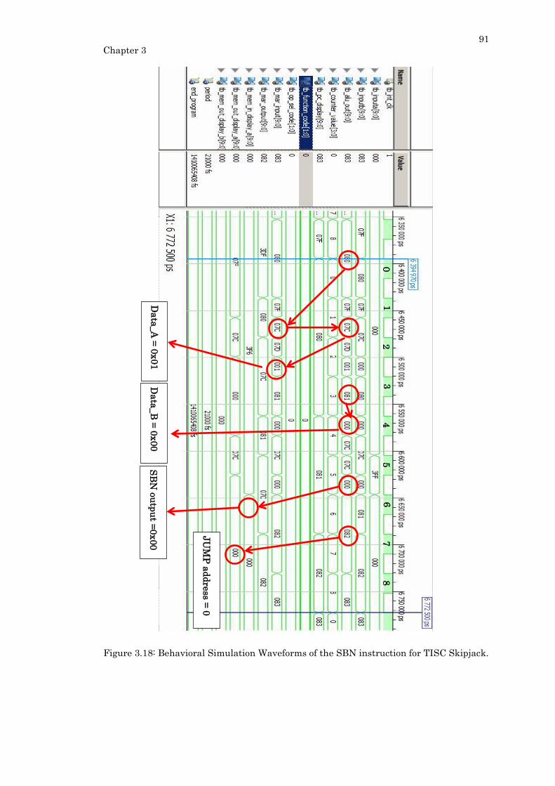
91
Chapter 3
Figure 3.18: Behavioral Simulation Waveforms of the SBN instruction for TISC Skipjack.
0
1
2
3
4
5
6
7
8
Da
ta_A
= 0
x01
D
ata
_B
= 0
x00
SB
N o
utp
ut =
0x00
JU
MP
ad
dre
ss =
0
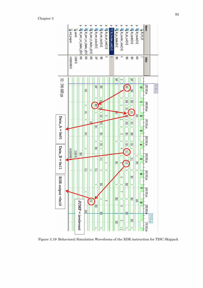
92
Chapter 3
Figure 3.19: Behavioral Simulation Waveforms of the XOR instruction for TISC Skipjack
0
1
2
3
4
5
6
7
8
Da
ta_A
= 0
x01
D
ata
_B
= 0
x11
JU
MP
= irre
levan
t
XO
R o
utp
ut =
0x10
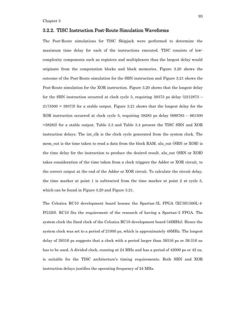
93
Chapter 3
3.2.2. TISC Instruction Post-Route Simulation Waveforms
The Post-Route simulations for TISC Skipjack were performed to determine the
maximum time delay for each of the instructions executed. TISC consists of low-
complexity components such as registers and multiplexers thus the largest delay would
originate from the computation blocks and block memories. Figure 3.20 shows the
outcome of the Post-Route simulation for the SBN instruction and Figure 3.21 shows the
Post-Route simulation for the XOR instruction. Figure 3.20 shows that the longest delay
for the SBN instruction occurred at clock cycle 5, requiring 39373 ps delay (2212873 –
2173500 = 39373) for a stable output. Figure 3.21 shows that the longest delay for the
XOR instruction occurred at clock cycle 5, requiring 38283 ps delay (699783 – 661500
=38283) for a stable output. Table 3.3 and Table 3.4 present the TISC SBN and XOR
instruction delays. The int_clk is the clock cycle generated from the system clock. The
mem_out is the time taken to read a data from the block RAM. alu_out (SBN or XOR) is
the time delay for the instruction to produce the desired result. alu_out (SBN or XOR)
takes consideration of the time taken from a clock triggers the Adder or XOR circuit, to
the correct output at the end of the Adder or XOR circuit. To calculate the circuit delay,
the time marker at point 1 is subtracted from the time marker at point 2 at cycle 5,
which can be found in Figure 3.20 and Figure 3.21.
The Celoxica RC10 development board houses the Spartan-3L FPGA (XC3S1500L-4-
FG320). RC10 fits the requirement of the research of having a Spartan-3 FPGA. The
system clock the fixed clock of the Celoxica RC10 development board (48MHz). Hence the
system clock was set to a period of 21000 ps, which is approximately 48MHz. The longest
delay of 39316 ps suggests that a clock with a period larger than 39316 ps or 39.316 ns
has to be used. A divided clock, running at 24 MHz and has a period of 42000 ps or 42 ns,
is suitable for the TISC architecture’s timing requirements. Both SBN and XOR
instruction delays justifies the operating frequency of 24 MHz.
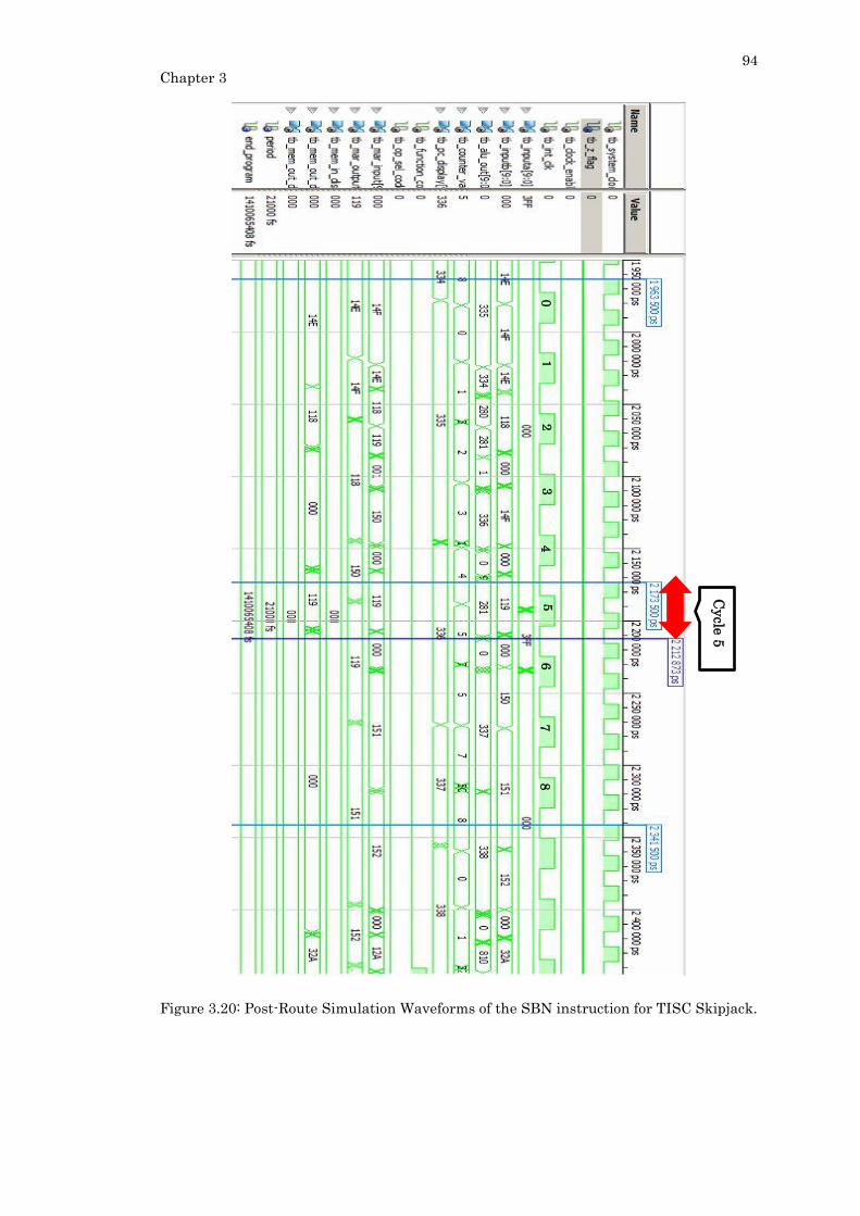
94
Chapter 3
Figure 3.20: Post-Route Simulation Waveforms of the SBN instruction for TISC Skipjack.
Cycle
5
0
1
2
3
4
5
6
7
8
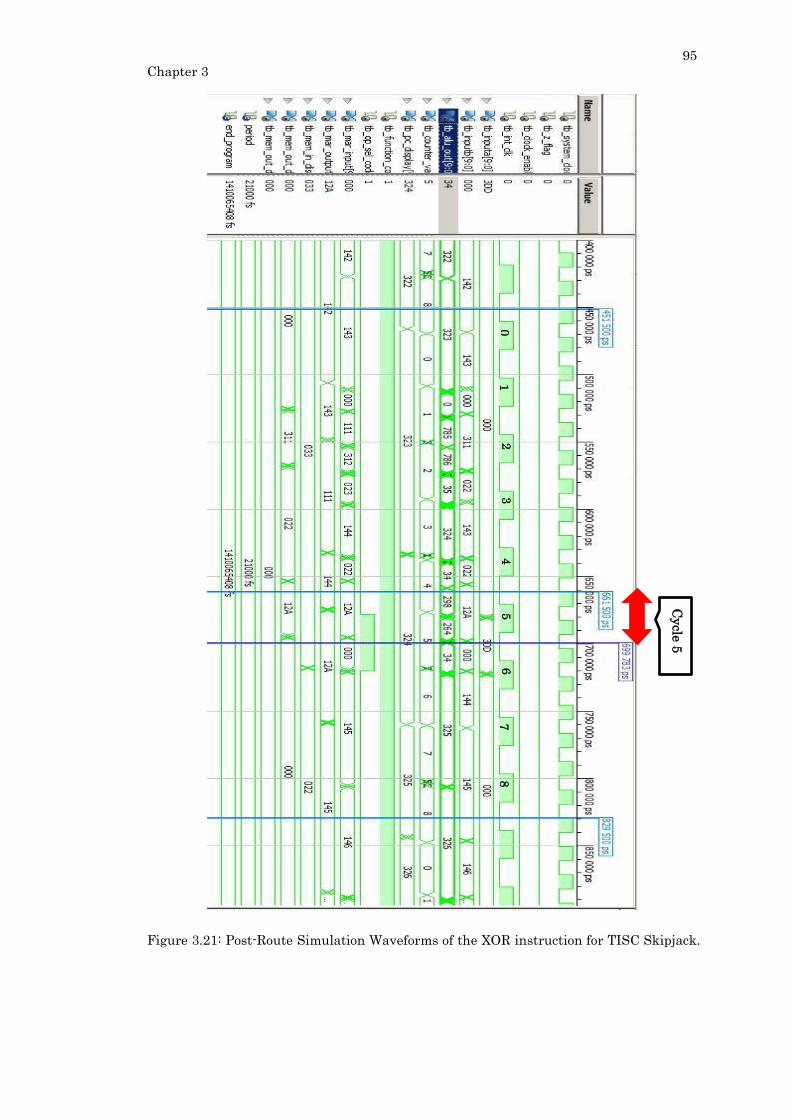
95
Chapter 3
Figure 3.21: Post-Route Simulation Waveforms of the XOR instruction for TISC Skipjack.
Cycle
5
0
1
2
4
5
6
3
7
8
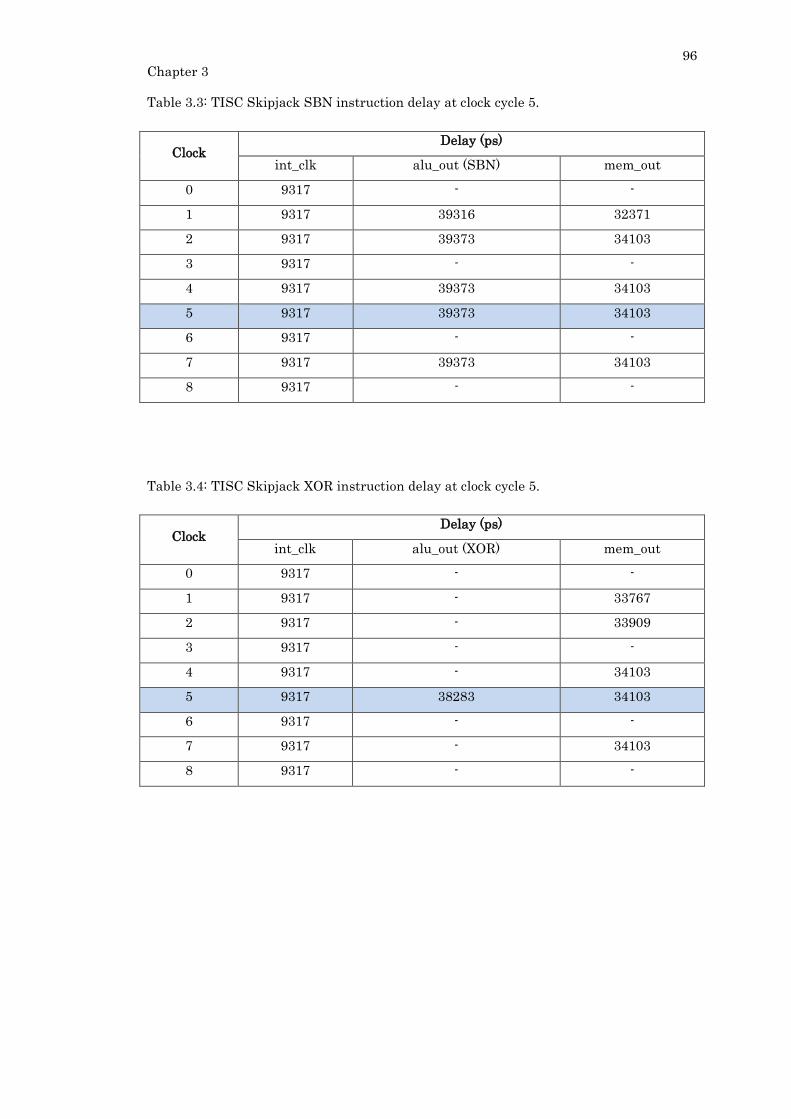
96
Chapter 3
Table 3.3: TISC Skipjack SBN instruction delay at clock cycle 5.
Clock Delay (ps)
int_clk alu_out (SBN) mem_out
0 9317 - -
1 9317 39316 32371
2 9317 39373 34103
3 9317 - -
4 9317 39373 34103
5 9317 39373 34103
6 9317 - -
7 9317 39373 34103
8 9317 - -
Table 3.4: TISC Skipjack XOR instruction delay at clock cycle 5.
Clock Delay (ps)
int_clk alu_out (XOR) mem_out
0 9317 - -
1 9317 - 33767
2 9317 - 33909
3 9317 - -
4 9317 - 34103
5 9317 38283 34103
6 9317 - -
7 9317 - 34103
8 9317 - -

97
Chapter 3
3.2.3. Design Behavioral Verification
The TISC Skipjack’s behavioral simulation is done using a test bench running at 24 MHz
(Period = 42 ns). The output of the encryption is compared to the output of the standard
Skipjack test vector. The test vector used was “33221100DDCCBBAA” as the input
plaintext in hexadecimal and a key value (also known as the crypto-variable [63]) of
“00998877665544332211” in hexadecimal. The TISC Skipjack produces the correct cipher
text at 1363855500 ps with a value of “2587CAE27A12D300” in hexadecimal. Figure 3.22
shows the waveform of the encrypted cipher text and Figure 3.23 shows the correct
ciphertext at 1363971794 ps in a Post-Route Simulation. The standard test vector used
in Figure 3.24 is provided by NIST, showing the cipher states with the corresponding key
and plaintext.
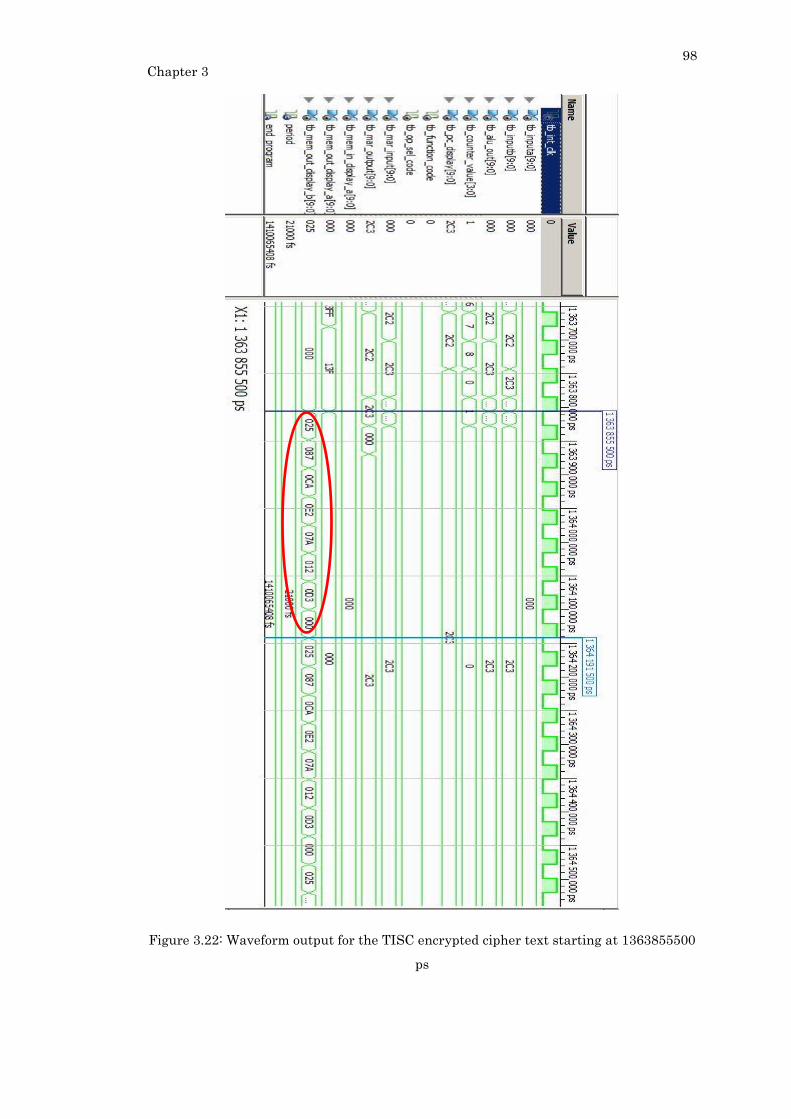
98
Chapter 3
Figure 3.22: Waveform output for the TISC encrypted cipher text starting at 1363855500
ps
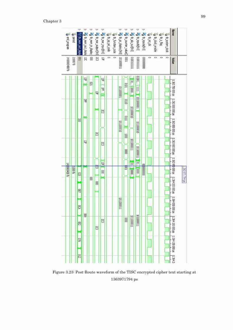
99
Chapter 3
Figure 3.23: Post-Route waveform of the TISC encrypted cipher text starting at
1363971794 ps
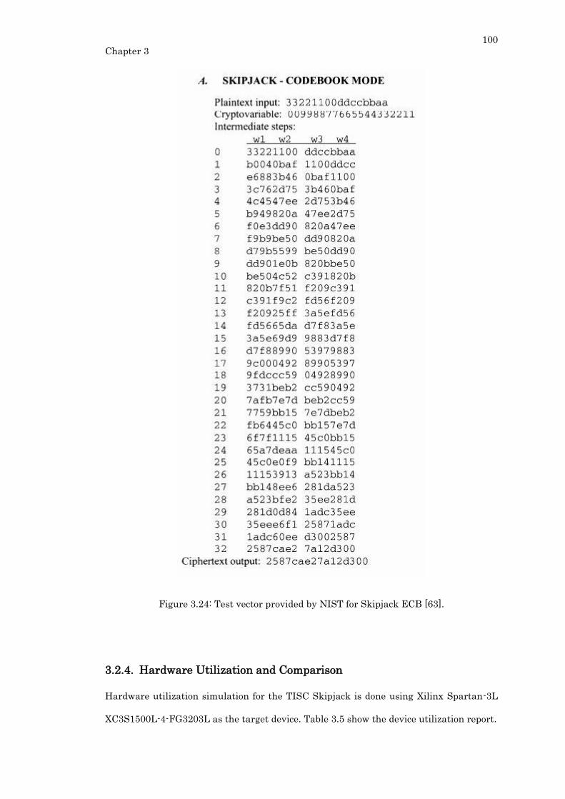
100
Chapter 3
Figure 3.24: Test vector provided by NIST for Skipjack ECB [63].
3.2.4. Hardware Utilization and Comparison
Hardware utilization simulation for the TISC Skipjack is done using Xilinx Spartan-3L
XC3S1500L-4-FG3203L as the target device. Table 3.5 show the device utilization report.
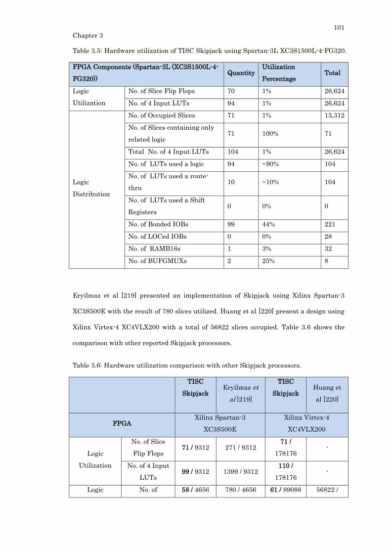
101
Chapter 3
Table 3.5: Hardware utilization of TISC Skipjack using Spartan-3L XC3S1500L-4-FG320.
FPGA Components (Spartan-3L (XC3S1500L-4-
FG320)) Quantity
Utilization
Percentage Total
Logic
Utilization
No. of Slice Flip Flops 70 1% 26,624
No. of 4 Input LUTs 94 1% 26,624
Logic
Distribution
No. of Occupied Slices 71 1% 13,312
No. of Slices containing only
related logic 71 100% 71
Total No. of 4 Input LUTs 104 1% 26,624
No. of LUTs used a logic 94 ~90% 104
No. of LUTs used a route-
thru 10 ~10% 104
No. of LUTs used a Shift
Registers 0 0% 0
No. of Bonded IOBs 99 44% 221
No. of LOCed IOBs 0 0% 28
No. of RAMB16s 1 3% 32
No. of BUFGMUXs 2 25% 8
Eryilmaz et al [219] presented an implementation of Skipjack using Xilinx Spartan-3
XC3S500E with the result of 780 slices utilized. Huang et al [220] present a design using
Xilinx Virtex-4 XC4VLX200 with a total of 56822 slices occupied. Table 3.6 shows the
comparison with other reported Skipjack processors.
Table 3.6: Hardware utilization comparison with other Skipjack processors.
TISC
Skipjack
Eryilmaz et
al [219]
TISC
Skipjack
Huang et
al [220]
FPGA Xilinx Spartan-3
XC3S500E
Xilinx Virtex-4
XC4VLX200
Logic
Utilization
No. of Slice
Flip Flops 71 / 9312 271 / 9312
71 /
178176 -
No. of 4 Input
LUTs 99 / 9312 1399 / 9312
110 /
178176 -
Logic No. of 58 / 4656 780 / 4656 61 / 89088 56822 /
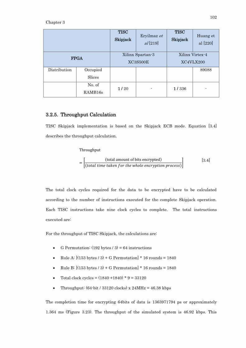
102
Chapter 3
TISC
Skipjack
Eryilmaz et
al [219]
TISC
Skipjack
Huang et
al [220]
FPGA Xilinx Spartan-3
XC3S500E
Xilinx Virtex-4
XC4VLX200
Distribution Occupied
Slices
89088
No. of
RAMB16s 1 / 20 - 1 / 336 -
3.2.5. Throughput Calculation
TISC Skipjack implementation is based on the Skipjack ECB mode. Equation [3.4]
describes the throughput calculation.
Throughput
= [(total amount of bits encrypted)
(𝑡𝑜𝑡𝑎𝑙 𝑡𝑖𝑚𝑒 𝑡𝑎𝑘𝑒𝑛 𝑓𝑜𝑟 𝑡ℎ𝑒 𝑤ℎ𝑜𝑙𝑒 𝑒𝑛𝑐𝑟𝑦𝑝𝑡𝑖𝑜𝑛 𝑝𝑟𝑜𝑐𝑒𝑠𝑠)] [3.4]
The total clock cycles required for the data to be encrypted have to be calculated
according to the number of instructions executed for the complete Skipjack operation.
Each TISC instructions take nine clock cycles to complete. The total instructions
executed are:
For the throughput of TISC Skipjack, the calculations are:
G Permutation: (192 bytes / 3) = 64 instructions
Rule A: [(153 bytes / 3) + G Permutation] * 16 rounds = 1840
Rule B: [(153 bytes / 3) + G Permutation] * 16 rounds = 1840
Total clock cycles = (1840 +1840) * 9 = 33120
Throughput: (64-bit / 33120 clocks) x 24MHz = 46.38 kbps
The completion time for encrypting 64bits of data is 1363971794 ps or approximately
1.364 ms (Figure 3.23). The throughput of the simulated system is 46.92 kbps. This
103
Chapter 3
calculation shows that the expected throughput and the calculated throughput of the
TISC Skipjack is correct with both results indicating a throughput of approximately 46
kbps. Table 3.7 show the comparison of TISC throughput with other Skipjack processors.
Table 3.7: Throughput comparison with other Skipjack processors.
TISC Skipjack Eryilmaz et al [219] Huang et al [220]
Throughput (kbps) 46.92 19393.9 1136000
3.3. Summary
A low-complexity, low-area TISC for Skipjack is designed and presented in this chapter.
To summarize, this chapter presents the following:
1) Modified URISC is used as a simplistic processor for lightweight cipher Skipjack.
2) TISC Skipjack occupies 71 slices using a Spartan3 XCS1500L-4 FPGA.
3) The TISC achieved a throughput of 46.92 kbps.
4) The TISC Skipjack is the smallest known design with a trade-off in terms of
throughput.
104
Chapter 4
CHAPTER 4
LOW-COMPLEXITY, LOW-AREA FPGA ENCRYPTION
ARCHITECTURE USING A MODERN CIPHER, THE
ADVANCED ENCRYPTION STANDARD (AES)
__________________________________________________________________________________
4.1. Method of the Proposed Improvement on the current S-Box
4.1.1. The Design of the Proposed Minimized S-Box
This proposed method aims to produce a bi-directional S-box with a gate count less than
the total of 192 gates from Boyar’s work [71, 212], which is the smallest know bi-
directional S-box. Figure 4.1 shows the proposed method uses Boyar’s forward S-box [212]
with additional identical circuit added before the input and after the output. This
modification makes a bi-directional S-box (similar to a composite field representation). A
forward S-Box in the composite field has the affine transformation in the process while
the Boyar’s three stage S-Box [71] represent the affine transformation embedded within
as a part of the circuit derived from matrix B (Chapter 2, figure 2.17). An inverse affine
circuit is the only circuit that determines the character of the inverse S-Box. Adding an
inverse affine transform at the end of the composite field S-box effectively cancels out the
transformation done by the affine transform in the forward S-Box. To complete the
Boyar’s Forward S-box circuit [212], another inverse affine transform has to be present
at the front-end as the completing component for the inverse S-box. This results to a
complete bi-directional S-Box. MUXs are required to choose the path of the data from
encryption and decryption mode selection.
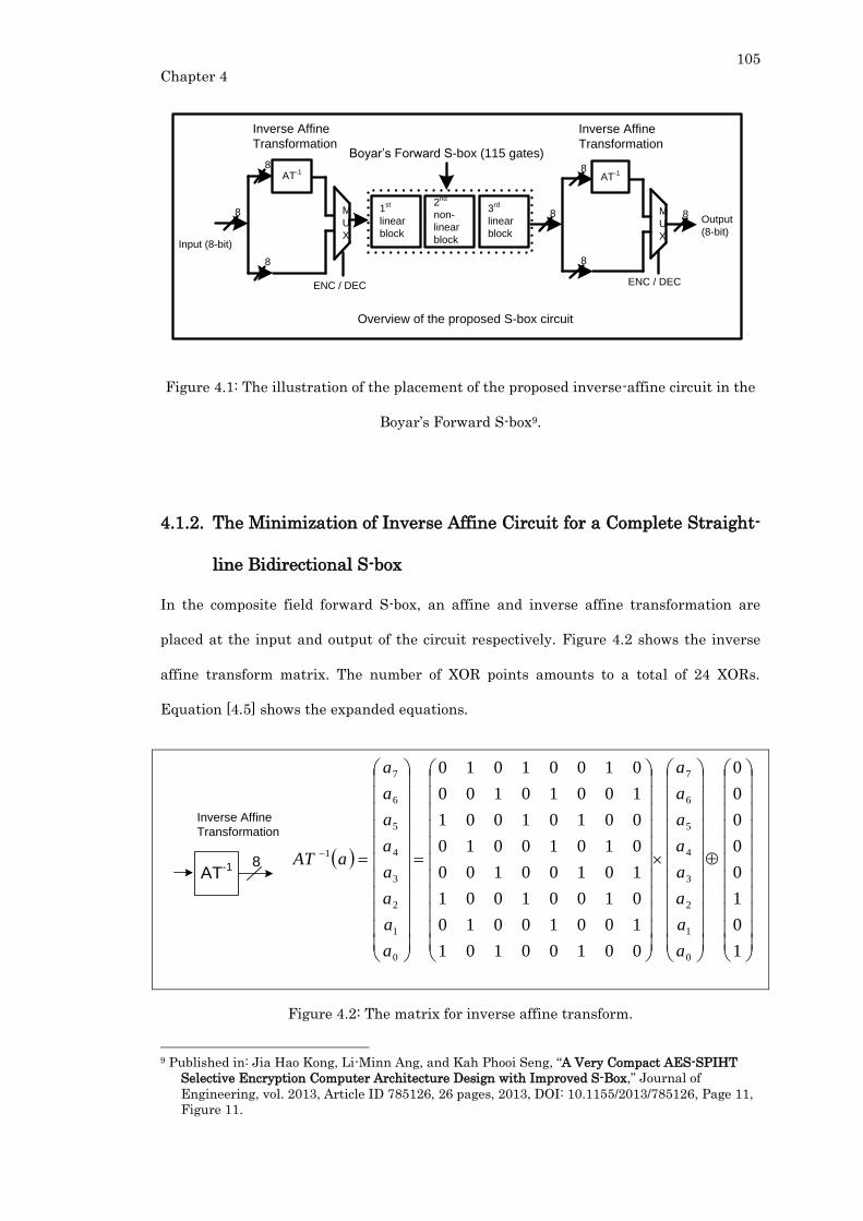
105
Chapter 4
Inverse Affine
Transformation
Input (8-bit)
8Output
(8-bit)
AT-1
8
8
8
8
8
8 M
U
X
ENC / DEC
M
U
X
ENC / DEC
2nd
non-
linear
block
1st
linear
block
3rd
linear
block
AT-1
Overview of the proposed S-box circuit
Boyar’s Forward S-box (115 gates)
Inverse Affine
Transformation
Figure 4.1: The illustration of the placement of the proposed inverse-affine circuit in the
Boyar’s Forward S-box9.
4.1.2. The Minimization of Inverse Affine Circuit for a Complete Straight-
line Bidirectional S-box
In the composite field forward S-box, an affine and inverse affine transformation are
placed at the input and output of the circuit respectively. Figure 4.2 shows the inverse
affine transform matrix. The number of XOR points amounts to a total of 24 XORs.
Equation [4.5] shows the expanded equations.
1
0
1
0
0
0
0
0
00100101
10010010
01001001
10100100
01010010
00101001
10010100
01001010
0
1
2
3
4
5
6
7
0
1
2
3
4
5
6
7
1
a
a
a
a
a
a
a
a
a
a
a
a
a
a
a
a
aATAT
-1
Inverse Affine
Transformation
8
Figure 4.2: The matrix for inverse affine transform.
9 Published in: Jia Hao Kong, Li-Minn Ang, and Kah Phooi Seng, “A Very Compact AES-SPIHT
Selective Encryption Computer Architecture Design with Improved S-Box,” Journal of
Engineering, vol. 2013, Article ID 785126, 26 pages, 2013, DOI: 10.1155/2013/785126, Page 11,
Figure 11.
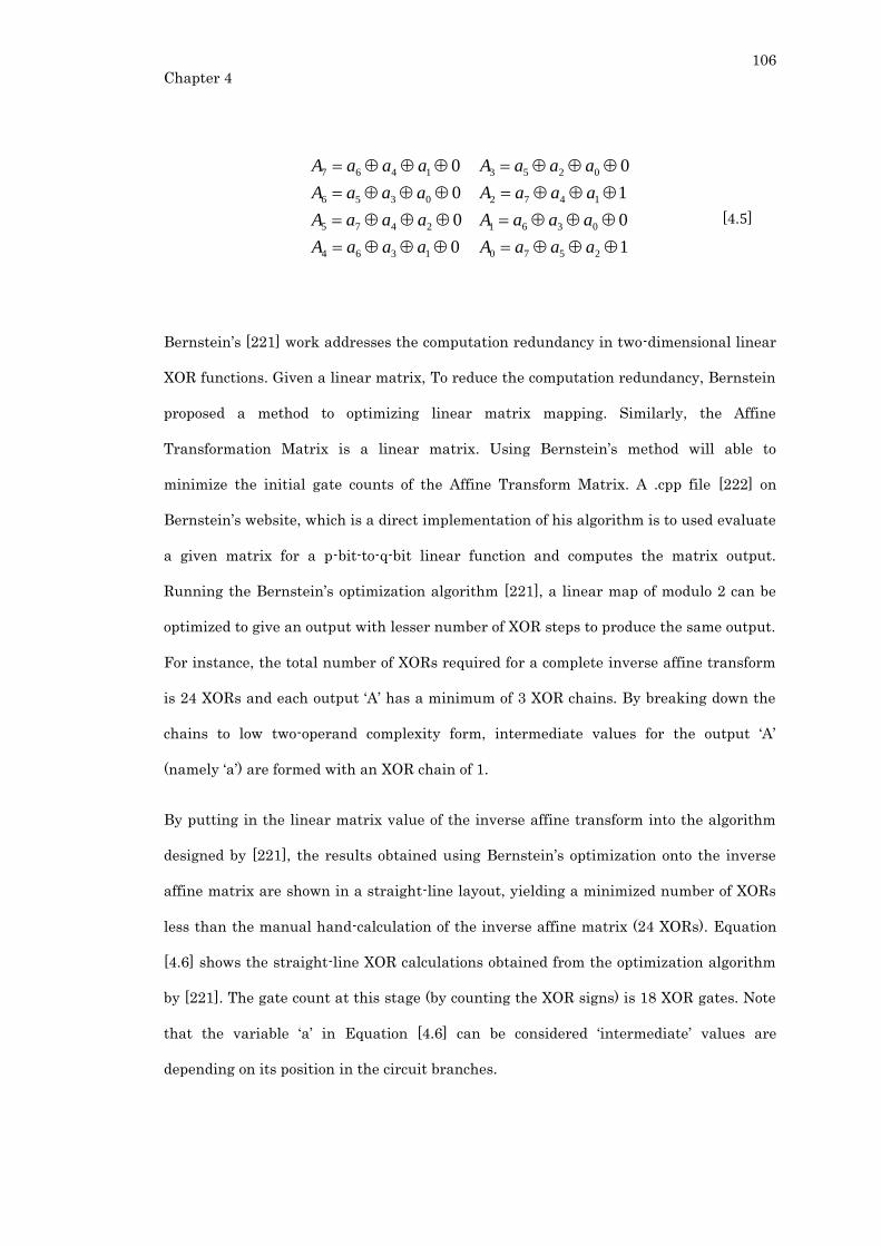
106
Chapter 4
1
0
1
0
0
0
0
0
2570
0361
1472
0253
1364
2475
0356
1467
aaaA
aaaA
aaaA
aaaA
aaaA
aaaA
aaaA
aaaA
[4.5]
Bernstein’s [221] work addresses the computation redundancy in two-dimensional linear
XOR functions. Given a linear matrix, To reduce the computation redundancy, Bernstein
proposed a method to optimizing linear matrix mapping. Similarly, the Affine
Transformation Matrix is a linear matrix. Using Bernstein’s method will able to
minimize the initial gate counts of the Affine Transform Matrix. A .cpp file [222] on
Bernstein’s website, which is a direct implementation of his algorithm is to used evaluate
a given matrix for a p-bit-to-q-bit linear function and computes the matrix output.
Running the Bernstein’s optimization algorithm [221], a linear map of modulo 2 can be
optimized to give an output with lesser number of XOR steps to produce the same output.
For instance, the total number of XORs required for a complete inverse affine transform
is 24 XORs and each output ‘A’ has a minimum of 3 XOR chains. By breaking down the
chains to low two-operand complexity form, intermediate values for the output ‘A’
(namely ‘a’) are formed with an XOR chain of 1.
By putting in the linear matrix value of the inverse affine transform into the algorithm
designed by [221], the results obtained using Bernstein’s optimization onto the inverse
affine matrix are shown in a straight-line layout, yielding a minimized number of XORs
less than the manual hand-calculation of the inverse affine matrix (24 XORs). Equation
[4.6] shows the straight-line XOR calculations obtained from the optimization algorithm
by [221]. The gate count at this stage (by counting the XOR signs) is 18 XOR gates. Note
that the variable ‘a’ in Equation [4.6] can be considered ‘intermediate’ values are
depending on its position in the circuit branches.
107
Chapter 4
13714159304
12013708303
1611173612647102
1521610811416201
67159510425100
aaaaxaaaa
aaaaxaxxa
aaaaxaaaaaaa
aaaaaaxxaxxa
axaaaaaaaxxa
[4.6]
This initial form of the minimized circuit uses a total of 18 XOR gates (which is less than
the initial count of 24 gates). By sorting out the variables, Equation [4.6] can be
minimized by expanding the equations shown in Equation [4.7]. The equations mapped
out show that there are only eight outputs at the end. Points shown below explain the
Equation [4.6] and Equation [4.7].
1. The variables: 𝑥0, 𝑥1, 𝑥2, 𝑥3, 𝑥4, 𝑥5, 𝑥6, 𝑥7 are the inputs to the inverse affine
matrix.
2. The final variables identified (the tip end of the circuit branches) are:
𝑎9, 𝑎10, 𝑎12, 𝑎13, 𝑎14, 𝑎15, 𝑎16, 𝑎17.
108
Chapter 4
75274254161117
7427412115216
7414176715
6416314313714
6316301012013
6303063612
5453043010811
530205329510
520205159
430430708
434131647
416
323121425
313010304
303
212010102
201
100
)()(
)()(
)(
)()(
)()(
)(
)()(
)()(
)(
)(
)()(
)()(
)()(
)()(
xxxxxxxxaaa
xxxxxxxxaaa
xxxxxxaxa
xxxxxxxxaaa
xxxxxxxxaaa
xxxxxxaxa
xxxxxxxxaaa
xxxxxxxxaaa
xxxxxxaxa
xxxxxxaxa
xxxxxxaaa
xxa
xxxxxxaaa
xxxxxxaaa
xxa
xxxxxxaaa
xxa
xxa
[4.7]
Equation [4.8] shows the alternate representation of Equation [4.7]. The current gate
count is 16 XOR gates. Note that from this point onwards, the minimization is done by
factor grouping since the circuit is small.
52093
741152
630121
752170
641147
530106
742165
631134
xxxaA
xxxaA
xxxaA
xxxaA
xxxaA
xxxaA
xxxaA
xxxaA
[4.8]
From here, minimization is done via factor grouping. In Equation [4.9] shows the
common bases that are first acquired from the expanded equations into their respective
outputs and Equation [4.10] shows the ‘intermediate’ XORs using ‘y’ representations,
which is eventually represented by ‘A’ as the final output.
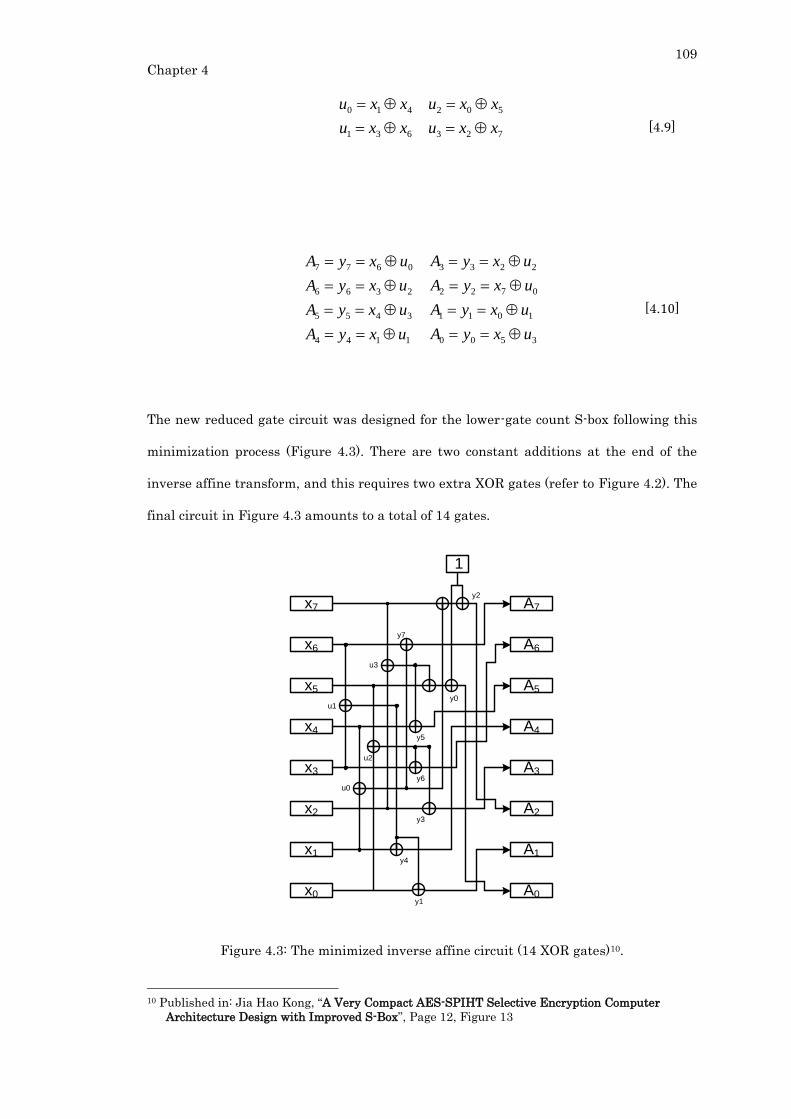
109
Chapter 4
723631
502410
xxuxxu
xxuxxu
[4.9]
3500
1011
0722
2233
1144
3455
2366
0677
uxyA
uxyA
uxyA
uxyA
uxyA
uxyA
uxyA
uxyA
[4.10]
The new reduced gate circuit was designed for the lower-gate count S-box following this
minimization process (Figure 4.3). There are two constant additions at the end of the
inverse affine transform, and this requires two extra XOR gates (refer to Figure 4.2). The
final circuit in Figure 4.3 amounts to a total of 14 gates.
x0
x1
x2
x3
x4
x5
x6
x7
A0
A1
A2
A3
A4
A5
A6
A7
u1
u3
u2
u0
y7
y6
y5
y4
y3
y1
y2
y0
1
Figure 4.3: The minimized inverse affine circuit (14 XOR gates)10.
10 Published in: Jia Hao Kong, “A Very Compact AES-SPIHT Selective Encryption Computer
Architecture Design with Improved S-Box”, Page 12, Figure 13

110
Chapter 4
By using the new circuit shown in Figure 4.3 and the original Boyar’s S-Box (Chapter 2
Literature Review, section 2.6.2, Figure 2.17), the final standalone S-Box is illustrated in
Figure 4.4, with built-in multiplexers (MUXs) with a total of 143 gates (Boyar (115 gates)
+ 2 * inverse affine circuit (which is 2*14 gates) excluding MUX 16 gates). Boyar [71] did
not include the MUX circuits. The final circuit is a straight line straight line circuit (with
one inverse affine circuit at both ends each).

111
Chapter 4
b0
b1
b2
b3
b4
b5
b6
b7
a1
a3
a2
a0
y7
y6
y5
y4
y3
y1
y2
y0
EN
C / D
EC
Inp
ut (8
-bit)
b0
b1
b2
b3
b4
b5
b6
b7
a1
a3
a2
a0
y7
y6
y5
y4
y3
y1
y2
y0
EN
C / D
EC
Ou
tpu
t (8-b
it)
y1
4
y1
3
y9
y8
t0
y1
y4
y1
2
y7
y6
y5
y4
y3
y2
y1
y0
y1
5
y1
4
y1
3
y1
2
y1
1
y1
0
y9
y8
y2
0
y1
9
y1
8
y1
7
y1
6
y2
1
y3
y5
y1
0
t1
y2
y1
5
y2
0
y6
y1
1y7 y1
7
y1
9
x7
x6
x5
x4
x3
x2
x1
x0
y1
6
y2
1
y1
8
z7
z6
z5
z4
z3
z2
z1
z0
z1
5
z1
4
z1
3
z1
2
z1
1
z1
0
z9
z8
z1
7
z1
6
t53
t54
t52
t49
t47
t46
t55
t48
t50
t56
t57
t51
t59
t58
t60
t61
t62
t63
t64
t65
t66
s3
s4
S7
S6
S5
S4
S3
S2
S1
S0
s1
t67
s2
s5
s6
s7
s0
t15
t12
t16
t13 t5t3t7
t8
t2
t4
t6t9
t10
t11
t14
t17
t18t1
9
t20
t21
t22
t23
t24
t25
t26 t2
7
t28
t29
t30
t31
t32
t33
t34 t35
t36
t37
t38
t39
t40
t41
Inve
rsio
n in
GF
(24)
t42
t43
t44
t45
z0
z1
z2
z3
z4
z5
z6
z7
z8
z9
z1
0
z1
1
z1
2
z1
3
z1
4
z1
5
z1
6
z1
7
Inve
rse
Affin
e
Tra
nsfo
rma
tion
Inp
ut (8
-bit)
8O
utp
ut
(8-b
it)
AT
-188
8
88
8MUX
EN
C / D
EC
MUX
EN
C / D
EC
2n
d
no
n-
line
ar
blo
ck
1st
line
ar
blo
ck
3rd
line
ar
blo
ck
AT
-1
Ove
rvie
w o
f the
min
imiz
ed
SB
OX
circ
uit
Min
imiz
ed
forw
ard
SB
OX
co
mp
on
en
ts
Inve
rse
Affin
e
Tra
nsfo
rma
tion
Figure 4.4: The complete gate layout of the proposed S-box configuration for bi-
directional setting11
11 Published in: Jia Hao Kong, “A Very Compact AES-SPIHT Selective Encryption Computer
Architecture Design with Improved S-Box”, Page 10, Figure 10.
112
Chapter 4
4.2. Development of the Compact Instruction Set Architecture for
the AES
To design a low-area, low-complexity system, mixed software-hardware architecture has
to be adopted and configured to a most desirable combination of compact code and
compact hardware. For this, the URISC is used to create a customized architecture called
the compact instruction set architecture (CISA). The reason it is called a CISA is due to
the minimized, and compacted instruction sets that the architecture accommodates.
There is no need for any additional instruction sets in order to complete all the AES
transformations, and, therefore, the computer architecture is ‘compact’. The latter part of
this section further explains and dissects the CISA AES architecture into the following
sub-sections: architecture, function codes and instruction sets, memory, FSM control
signals and cipher algorithm program code.
4.2.1. The New Data-path Architecture and Arithmetic –Logic Unit (ALU)
In the AES transformations, there are two specific circuits required: a circuit for
SubBytes and MixColumns. As for the ShiftRow and AddRoundKey, a simple XOR and
memory readdressing would suffice. As for the SubBytes, a combinational circuit has to
be present. In this part of the work, the proposed S-box in Section 4.1 is used as a one of
the computation blocks. As for MixColumns, kindly refer to [65] for the xTime dedicated
four XOR hardware because of the simplistic nature and compatibility . Unlike URISC,
which uses only one instruction, the proposed CISA AES uses four minimized
instructions (including SBN) to perform the complete AES encryption process. The CISA
ALU includes: Adder, XOR, xTime, and S-box.
The novel CISA data-path is shown in Figure 4.5. It has a single memory unit to store
both program and data for the AES algorithm. With the SBN instruction (similar to
URISC), the CISA can branch to any PC values within the memory unit and execute any

113
Chapter 4
instructions in any location of the memory unit. With seven registers, five multiplexers,
one memory unit and four ALU blocks, the CISA is complete and functional. Similar to
the structure of URISC, the CISA data-path loads in the first memory address and
subsequently loads in the first data item. This operation is repeated for the second data
item. Once both data are loaded into the CISA, they are sent to the ALU for computation
and the outputs will be chosen regarding the function code embedded in the first address
loaded. The function code is a 2-bit value, concatenated to the first data address in the
memory unit. With the 2-bit MSB value, the architecture can determine which
instruction is used for the current processor cycle and what data are stored back to the
memory.

114
Chapter 4
The Compact Reconfigurable ALU Design Space
MD
R
MA
R
MAR_SEL
[9:8]
FUNC_WRITE
MU
X1
0
RR’
0
MEMORY
UNIT
READ WRITE
N
CIN
FC
AES Processor
Adder
Z_IN
Z
N_IN
MU
X0
00
11
01
1
MUX1 0
PC_IN MDR_IN
MAR_IN
COMP_SEL
PC
0
MUX0 1
MUX0 1 PC_OUT_SEL
PC_OUT
MEM_OUT
MDR_OUTINPUT_B
INPUT_A
R_WRITE
MEM_OUT
ALU_OUT
ALU_SEL
A
B
C
xTime
xTime_Out
N
Z_WRITE Z
N_WRITEXOR
XOR_Out
Sub
Bytes
Sub Bytes_Out
Adder
Adder_Out
FUNC
Code ALU Output Mux
ALU_Out
FSM4-bit Counter
CISA AES
(Data-path)
Control
Signals
Figure 4.5: The novel CISA architecture, data-path and the ALU121314.
12 Published in: Jia Hao Kong, “A Very Compact AES-SPIHT Selective Encryption Computer
Architecture Design with Improved S-Box”, Page 16, Figure 17. 13 Published in: Jia Hao Kong, Li-Minn Ang, Kah Phooi Seng, Achonu Oluwole Adejo, “Minimal
Instruction Set FPGA AES Processor using Handel-C”, Proceedings of the 2010 International
Conference on Computer Applications and Industrial Electronics (ICCAIE 2010), CD-ROM: pp.
337-341, ISBN: 978-1-4244-9053-0, 2010. 14 Published in: J. H. Kong, L. -M. Ang, K. P. Seng, "MISC Processor for AES Encryption and
Decryption", Proceedings of 2011 International Conference on Embedded Systems & Intelligent
Technology (ICESIT 2011), pp.46-51, CD paper no: 00017, 2011.

115
Chapter 4
The architecture has two input parameters into the CISA: Input_A and Input_B. Like a
URISC, the architecture is also controlled by an FSM, the data movement and processing
are fixed within nine clock cycles. The Adder and XOR block takes in two data items and
perform bit-wise addition and XOR onto their respective inputs. The xTime block is a
part of the MixColumns transformation. In [93], by using the sub-structure computation
of a byte and between the computations of four bytes in an array of bytes, the derivation
of the MixColumns transformation can be defined. In [191], the implementation of an
‘xTime’ function is used to complete the multiplication of with ‘02’, modulo the irreducible
polynomial m(x) = x8 + x4 + x3 + x + 1. It is known that the MixColumns transformation
is a process involving several XOR processes and xTime processes. The xTime is a bit-
wise XOR operation that yields the constant multiplication by (02). By concatenating two
xTime blocks in serial, constant multiplication by (04) can be achieved. The MixColumns
circuit in [93] can be used for both MixColumns and Inverse MixColumns. In Figure 4.7,
part 1 of the circuit is the Mix Columns Transformation. Part 1 together with part 2 of
the circuit yields the Inverse MixColumns Transformation. The xTime circuit is shown in
Figure 4.6. The circuit in Figure 4.7 is translated to soft-codes, using the xTime circuit to
reproduce the exact output of the complete MixColumns operation.
To standardize the width of the register and data-path for the best design at the
architecture level, a unified and shared bit-wise XOR block will be used to perform a
XOR MOVE operations instead of the SBN MOVE to improve program memory efficiency
(XOR MOVE requires one less instruction less than SBN MOVE). The xTime circuit uses
three independent XORs.
b7
b6
b5
b4
b3
b2
b1
b0
a7
a6
a5
a4
a3
a2
a1
a0
Figure 4.6: The xTime circuit (Image redrawn from [223]).

116
Chapter 4
S2,cS0,c S1,c S3,c
XTime XTimeXTime XTime
XTime
XTime
XTime
XTime
Pa
rt I
Pa
rt II
XTime
S’2,cS’0,c S’1,cS’3,c
S’2,cS’0,c S’1,cS’3,c
Figure 4.7: The MixColumns Transformation Process using the xTime Circuit (Image
redrawn from [223]).
4.2.2. Application Specific Function Codes and Instruction Sets
To perform AES computations onto the plaintext, byte-oriented operations are adopted
from the AES algorithm. To perform tasks such as SubBytes and MixColumns, a new set
of instructions is developed. The CISA instruction sets shown in Table 4.1 are
differentiated using the two MSB of each of the instructions. The four instruction sets
used to perform different operations are showed in the Figure 4.8. These pseudo-codes
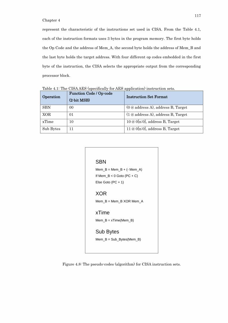
117
Chapter 4
represent the characteristic of the instructions set used in CISA. From the Table 4.1,
each of the instruction formats uses 3 bytes in the program memory. The first byte holds
the Op Code and the address of Mem_A, the second byte holds the address of Mem_B and
the last byte holds the target address. With four different op codes embedded in the first
byte of the instruction, the CISA selects the appropriate output from the corresponding
processor block.
Table 4.1: The CISA AES (specifically for AES application) instruction sets.
Operation Function Code / Op-code
(2-bit MSB) Instruction Set Format
SBN 00 (0 @ address A), address B, Target
XOR 01 (1 @ address A), address B, Target
xTime 10 10 @ 0[n:0], address B, Target
Sub Bytes 11 11 @ 0[n:0], address B, Target
SBN
Mem_B = Mem_B + (- Mem_A)
If Mem_B < 0 Goto (PC + C)
Else Goto (PC + 1)
XOR
Mem_B = Mem_B XOR Mem_A
xTime
Mem_B = xTime(Mem_B)
Sub Bytes
Mem_B = Sub_Bytes(Mem_B)
Figure 4.8: The pseudo-codes (algorithm) for CISA instruction sets.

118
Chapter 4
4.2.3. Memory Mapping and Program Structure
The CISA AES architecture includes a 1024 x 10-bit memory unit. The size of the
memory is determined by the size of the AES program and the data. The total available
memory is 1024 x 8-bit (512 bytes), which accommodates both the data and program
codes. The data section is located at the address location of 0 to 127, whereas the
program section takes the location of 128 to 1024. In the program section, instructions
are sorted in a sequence as the CISA executes in accordance. In the data section, the
breakdown of the memory allocation the plain text, master key and other temporary
variables are shown in Figure 4.9.
Data Section
Plain Text
Temporary Data Locations
Original Cipher Key
Temporary Data Locations
Rcon[i]
Cipher Text
Temporary Mix Column Data
Temporary Variables
Sub Keys (Expanded Keys)
Program Section
Shift Row
Add Round Key (Enc / Dec)
Key Expansion
Sub Bytes (Enc / Dec)
Mix Columns (Part 1)
Mix Columns (Part 2)
Loop
END
Inverse Shift Row
Figure 4.9: The Memory Mapping for CISA AES15.
For the program design of the CISA AES, functions and modules of a set of the written
instructions can be reused for code efficiency. During the decryption round, the Key
Expansion algorithm has to be executed, and the sub keys are stored inside the memory
unit. During encryption mode, the program sequence has to start by producing all the
sub keys and then proceed to the AddRoundKey function. Loop1 and Loop2 are used to
branch to any designated memory locations in the memory unit if the resultant value is
less than zero of negative. In loop1 and loop2, the addressed memory stores a number
15Published in: Jia Hao Kong, “A Very Compact AES-SPIHT Selective Encryption Computer
Architecture Design with Improved S-Box”, Page 19, Figure 20.
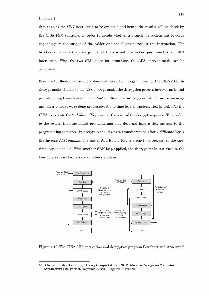
119
Chapter 4
that enables the SBN instruction to be executed and hence, the results will be check by
the CISA FSM controller in order to decide whether a branch instruction has to occur
depending on the output of the Adder and the function code of the instruction. The
function code tells the data-path that the current instruction performed is an SBN
instruction. With the two SBN loops for branching, the AES encrypt mode can be
completed.
Figure 4.10 illustrates the encryption and decryption program flow for the CISA AES. In
decrypt mode, similar to the AES encrypt mode, the decryption process involves an initial
pre-whitening transformation of AddRoundKey. The sub keys are stored in the memory
unit after encrypt were done previously. A one-time loop is implemented in order for the
CISA to execute the ‘AddRoundKey’ once at the start of the decrypt sequence. This is due
to the reason that the initial pre-whitening step does not have a flow pattern to the
programming sequence. In decrypt mode, the data transformation after AddRoundKey is
the Inverse MixColumns. The initial Add Round Key is a one-time process, so the one-
time loop is applied. With another SBN loop applied, the decrypt mode can execute the
four inverse transformations with ten iterations.
Shift Row
Sub Bytes
Check Loop1
If Loop1 is
Negative, jump
to Add Key.
Else, proceed.
Mix Column
Add Key
If Loop2 is
Negative, jump
to END.
Else, proceed.
END
Program Start
(ENCRYPT)Key Generation
Check Loop2
Inv Shift Row
Inv Sub Bytes
Check Loop1
If Loop1 is
Negative, jump
to END.
Else, proceed.
Inv Mix Column
Add Key
END
Program Start
(DECRYPT)
One Time LoopGo to Inv Shift
Row after 1st
key added
Figure 4.10: The CISA AES encryption and decryption program flowchart and structure16.
16Published in: Jia Hao Kong, “A Very Compact AES-SPIHT Selective Encryption Computer
Architecture Design with Improved S-Box”, Page 20, Figure 21.
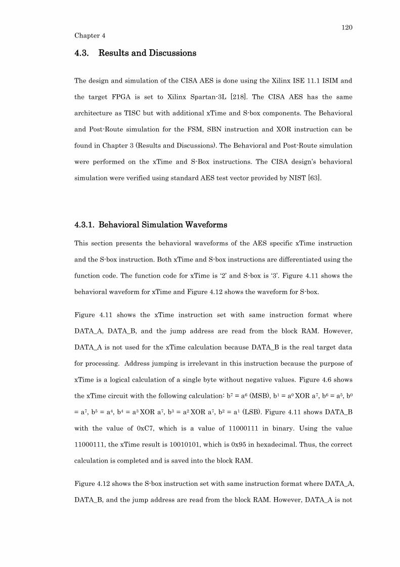
120
Chapter 4
4.3. Results and Discussions
The design and simulation of the CISA AES is done using the Xilinx ISE 11.1 ISIM and
the target FPGA is set to Xilinx Spartan-3L [218]. The CISA AES has the same
architecture as TISC but with additional xTime and S-box components. The Behavioral
and Post-Route simulation for the FSM, SBN instruction and XOR instruction can be
found in Chapter 3 (Results and Discussions). The Behavioral and Post-Route simulation
were performed on the xTime and S-Box instructions. The CISA design’s behavioral
simulation were verified using standard AES test vector provided by NIST [63].
4.3.1. Behavioral Simulation Waveforms
This section presents the behavioral waveforms of the AES specific xTime instruction
and the S-box instruction. Both xTime and S-box instructions are differentiated using the
function code. The function code for xTime is ‘2’ and S-box is ‘3’. Figure 4.11 shows the
behavioral waveform for xTime and Figure 4.12 shows the waveform for S-box.
Figure 4.11 shows the xTime instruction set with same instruction format where
DATA_A, DATA_B, and the jump address are read from the block RAM. However,
DATA_A is not used for the xTime calculation because DATA_B is the real target data
for processing. Address jumping is irrelevant in this instruction because the purpose of
xTime is a logical calculation of a single byte without negative values. Figure 4.6 shows
the xTime circuit with the following calculation: b7 = a6 (MSB), b1 = a0 XOR a7, b6 = a5, b0
= a7, b5 = a4, b4 = a3 XOR a7, b3 = a2 XOR a7, b2 = a1 (LSB). Figure 4.11 shows DATA_B
with the value of 0xC7, which is a value of 11000111 in binary. Using the value
11000111, the xTime result is 10010101, which is 0x95 in hexadecimal. Thus, the correct
calculation is completed and is saved into the block RAM.
Figure 4.12 shows the S-box instruction set with same instruction format where DATA_A,
DATA_B, and the jump address are read from the block RAM. However, DATA_A is not

121
Chapter 4
used for the S-box calculation because DATA_B is the real target data for processing.
Address jumping is irrelevant in this instruction because the purpose of S-box is a byte
substitution of a single byte without negative values. Figure 4.12 shows DATA_B with
the value of 0x60. Using the value 0x60 to refer to the S-box table shown in Table 2.9, the
S-box substitution result is 0xD0. Thus, the correct calculation is completed and is saved
into the block RAM.
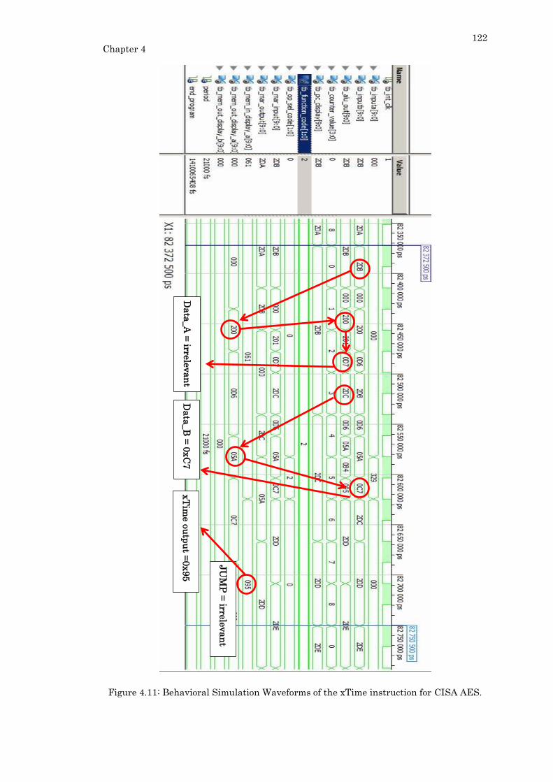
122
Chapter 4
Figure 4.11: Behavioral Simulation Waveforms of the xTime instruction for CISA AES.
Da
ta_A
= irre
levan
t D
ata
_B
= 0
xC
7
JU
MP
= irre
levan
t
xT
ime o
utp
ut =
0x95
123
Chapter 4
Figure 4.12: Behavioral Simulation Waveforms of the S-Box instruction for CISA AES.
Da
ta_A
= irre
levan
t D
ata
_B
= 0
x60
JU
MP
= irre
levan
t
SB
OX
ou
tpu
t =0xD
0
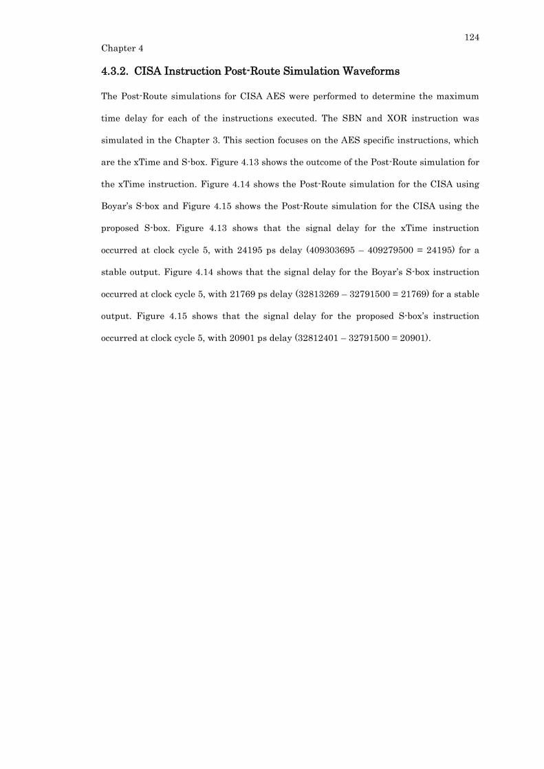
124
Chapter 4
4.3.2. CISA Instruction Post-Route Simulation Waveforms
The Post-Route simulations for CISA AES were performed to determine the maximum
time delay for each of the instructions executed. The SBN and XOR instruction was
simulated in the Chapter 3. This section focuses on the AES specific instructions, which
are the xTime and S-box. Figure 4.13 shows the outcome of the Post-Route simulation for
the xTime instruction. Figure 4.14 shows the Post-Route simulation for the CISA using
Boyar’s S-box and Figure 4.15 shows the Post-Route simulation for the CISA using the
proposed S-box. Figure 4.13 shows that the signal delay for the xTime instruction
occurred at clock cycle 5, with 24195 ps delay (409303695 – 409279500 = 24195) for a
stable output. Figure 4.14 shows that the signal delay for the Boyar’s S-box instruction
occurred at clock cycle 5, with 21769 ps delay (32813269 – 32791500 = 21769) for a stable
output. Figure 4.15 shows that the signal delay for the proposed S-box’s instruction
occurred at clock cycle 5, with 20901 ps delay (32812401 – 32791500 = 20901).

125
Chapter 4
Figure 4.13: Post-Route Simulation Waveforms of the xTime instruction for CISA AES.
Cycle
5
0
1
2
3
4
5
6
7
8
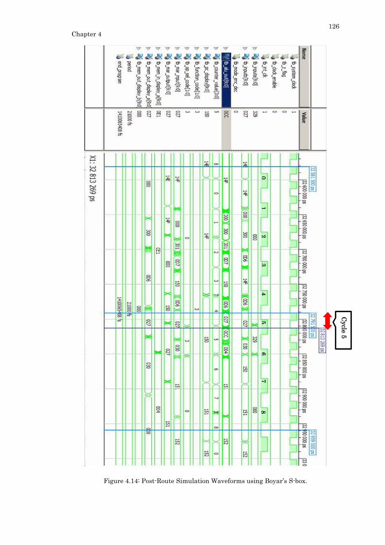
126
Chapter 4
Figure 4.14: Post-Route Simulation Waveforms using Boyar’s S-box.
Cycle
5
8
0
1
2
3
4
5
6
7

127
Chapter 4
Figure 4.15: Post-Route Simulation Waveforms using the proposed S-box.
Cycle
5
0
1
2
3
4
5
6
7
8

128
Chapter 4
Table 4.2 present the CISA xTime delays. Table 4.3 and Table 4.4 and S-box instruction
delays using Boyar’s S-box and the proposed S-box respectively. The int_clk is the clock
cycle generated from the system clock. The mem_out is the time taken to read a data
from the block RAM. alu_out (xTime or S-box) is the time delay for the instruction to
produce the desired result. alu_out (xTime or S-box) takes consideration of the time
taken from a clock triggers the xTime or S-box circuit, to the correct output at the end of
the xTime or S-box circuit. To calculate the circuit delay, the time marker at point 1 is
subtracted from the time marker at point 2 at cycle 5, which can be found in Figure 4.13,
Figure 4.14, and Figure 4.15.
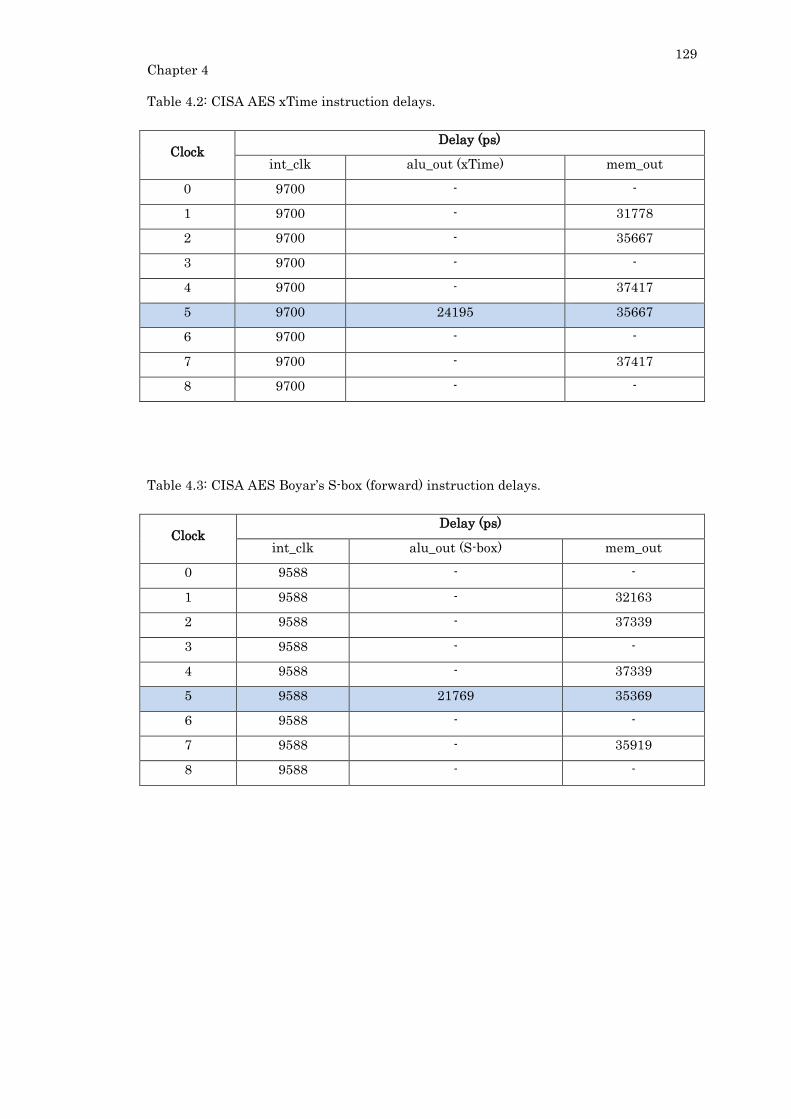
129
Chapter 4
Table 4.2: CISA AES xTime instruction delays.
Clock Delay (ps)
int_clk alu_out (xTime) mem_out
0 9700 - -
1 9700 - 31778
2 9700 - 35667
3 9700 - -
4 9700 - 37417
5 9700 24195 35667
6 9700 - -
7 9700 - 37417
8 9700 - -
Table 4.3: CISA AES Boyar’s S-box (forward) instruction delays.
Clock Delay (ps)
int_clk alu_out (S-box) mem_out
0 9588 - -
1 9588 - 32163
2 9588 - 37339
3 9588 - -
4 9588 - 37339
5 9588 21769 35369
6 9588 - -
7 9588 - 35919
8 9588 - -
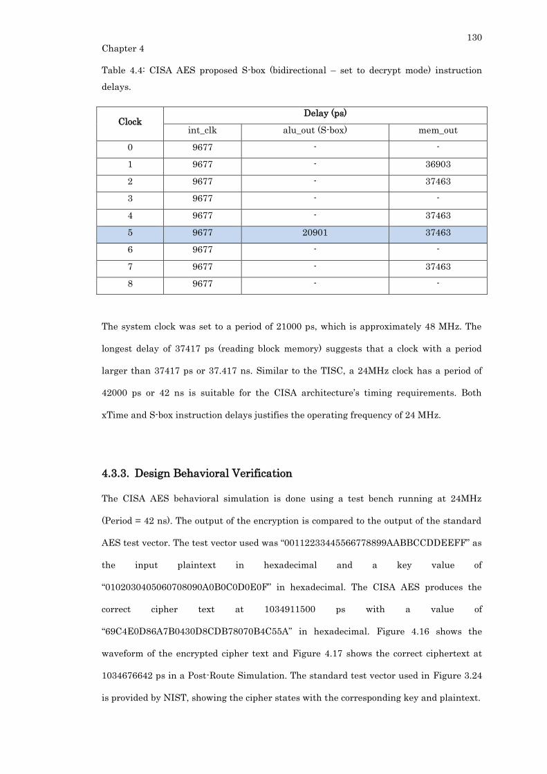
130
Chapter 4
Table 4.4: CISA AES proposed S-box (bidirectional – set to decrypt mode) instruction
delays.
Clock Delay (ps)
int_clk alu_out (S-box) mem_out
0 9677 - -
1 9677 - 36903
2 9677 - 37463
3 9677 - -
4 9677 - 37463
5 9677 20901 37463
6 9677 - -
7 9677 - 37463
8 9677 - -
The system clock was set to a period of 21000 ps, which is approximately 48 MHz. The
longest delay of 37417 ps (reading block memory) suggests that a clock with a period
larger than 37417 ps or 37.417 ns. Similar to the TISC, a 24MHz clock has a period of
42000 ps or 42 ns is suitable for the CISA architecture’s timing requirements. Both
xTime and S-box instruction delays justifies the operating frequency of 24 MHz.
4.3.3. Design Behavioral Verification
The CISA AES behavioral simulation is done using a test bench running at 24MHz
(Period = 42 ns). The output of the encryption is compared to the output of the standard
AES test vector. The test vector used was “00112233445566778899AABBCCDDEEFF” as
the input plaintext in hexadecimal and a key value of
“0102030405060708090A0B0C0D0E0F” in hexadecimal. The CISA AES produces the
correct cipher text at 1034911500 ps with a value of
“69C4E0D86A7B0430D8CDB78070B4C55A” in hexadecimal. Figure 4.16 shows the
waveform of the encrypted cipher text and Figure 4.17 shows the correct ciphertext at
1034676642 ps in a Post-Route Simulation. The standard test vector used in Figure 3.24
is provided by NIST, showing the cipher states with the corresponding key and plaintext.

131
Chapter 4
Figure 4.16: Waveform output for the CISA encrypted cipher text starting at 1034911500
ps.
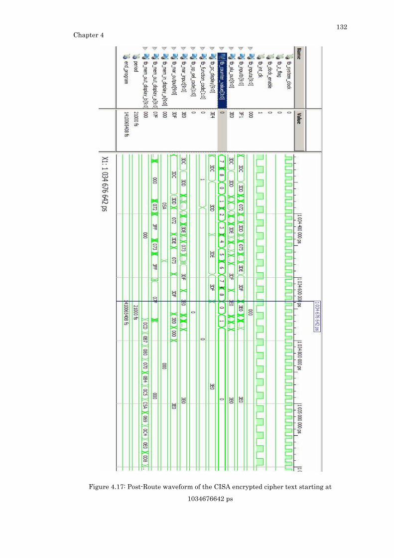
132
Chapter 4
Figure 4.17: Post-Route waveform of the CISA encrypted cipher text starting at
1034676642 ps

133
Chapter 4
Figure 4.18: Test vector provided by NIST for AES ECB [224].
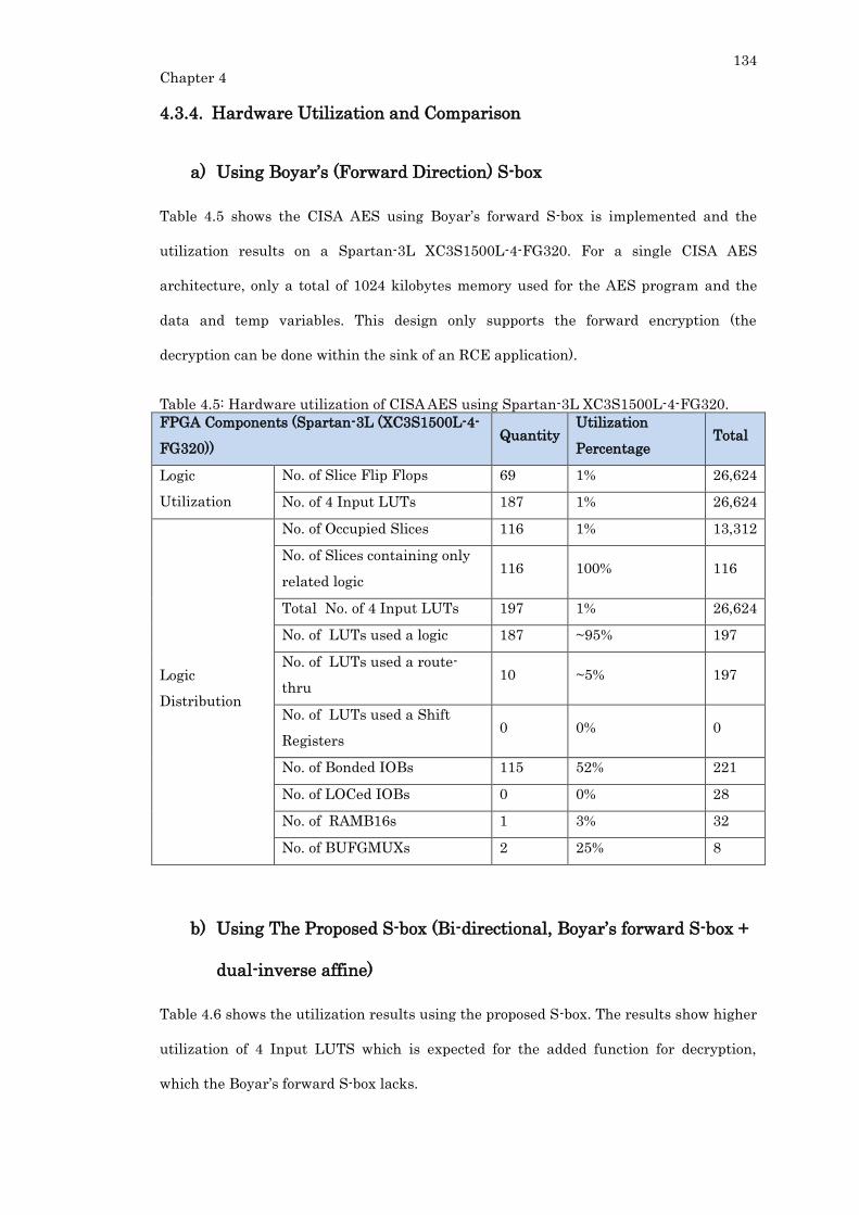
134
Chapter 4
4.3.4. Hardware Utilization and Comparison
a) Using Boyar’s (Forward Direction) S-box
Table 4.5 shows the CISA AES using Boyar’s forward S-box is implemented and the
utilization results on a Spartan-3L XC3S1500L-4-FG320. For a single CISA AES
architecture, only a total of 1024 kilobytes memory used for the AES program and the
data and temp variables. This design only supports the forward encryption (the
decryption can be done within the sink of an RCE application).
Table 4.5: Hardware utilization of CISA AES using Spartan-3L XC3S1500L-4-FG320.
FPGA Components (Spartan-3L (XC3S1500L-4-
FG320)) Quantity
Utilization
Percentage Total
Logic
Utilization
No. of Slice Flip Flops 69 1% 26,624
No. of 4 Input LUTs 187 1% 26,624
Logic
Distribution
No. of Occupied Slices 116 1% 13,312
No. of Slices containing only
related logic 116 100% 116
Total No. of 4 Input LUTs 197 1% 26,624
No. of LUTs used a logic 187 ~95% 197
No. of LUTs used a route-
thru 10 ~5% 197
No. of LUTs used a Shift
Registers 0 0% 0
No. of Bonded IOBs 115 52% 221
No. of LOCed IOBs 0 0% 28
No. of RAMB16s 1 3% 32
No. of BUFGMUXs 2 25% 8
b) Using The Proposed S-box (Bi-directional, Boyar’s forward S-box +
dual-inverse affine)
Table 4.6 shows the utilization results using the proposed S-box. The results show higher
utilization of 4 Input LUTS which is expected for the added function for decryption,
which the Boyar’s forward S-box lacks.
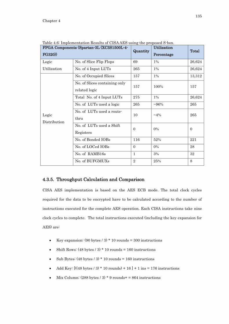
135
Chapter 4
Table 4.6: Implementation Results of CISA AES using the proposed S-box.
FPGA Components (Spartan-3L (XC3S1500L-4-
FG320)) Quantity
Utilization
Percentage Total
Logic
Utilization
No. of Slice Flip Flops 69 1% 26,624
No. of 4 Input LUTs 265 1% 26,624
Logic
Distribution
No. of Occupied Slices 157 1% 13,312
No. of Slices containing only
related logic 157 100% 157
Total No. of 4 Input LUTs 275 1% 26,624
No. of LUTs used a logic 265 ~96% 265
No. of LUTs used a route-
thru 10 ~4% 265
No. of LUTs used a Shift
Registers 0 0% 0
No. of Bonded IOBs 116 52% 221
No. of LOCed IOBs 0 0% 28
No. of RAMB16s 1 3% 32
No. of BUFGMUXs 2 25% 8
4.3.5. Throughput Calculation and Comparison
CISA AES implementation is based on the AES ECB mode. The total clock cycles
required for the data to be encrypted have to be calculated according to the number of
instructions executed for the complete AES operation. Each CISA instructions take nine
clock cycles to complete. The total instructions executed (including the key expansion for
AES) are:
Key expansion: (90 bytes / 3) * 10 rounds = 300 instructions
Shift Rows: (48 bytes / 3) * 10 rounds = 160 instructions
Sub Bytes: (48 bytes / 3) * 10 rounds = 160 instructions
Add Key: [((48 bytes / 3) * 10 rounds) + 16 ] + 1 ins = 176 instructions
Mix Column: (288 bytes / 3) * 9 rounds+ = 864 instructions

136
Chapter 4
Total AES instructions used for a 128-bit / 16-byte encryption = (300 + 160 + 160
+ 176 + 864) = 1660 instructions
Total bytes used in programming: (1012-128+1) = 884 bytes
Total bytes used for AES operations = 525 bytes
Total bytes used for other operations = 360 bytes
Total instructions used for other operations in complete 10 rounds of AES: (360 /
3) * 10 rounds = 1200 instructions
Grand total amount of instructions used for a complete 128-bit encryption: 1660
+ 1200 = 2860 instructions
The total amount of time period for the complete AES encryption is: 2860 x 9
cycles = 25740 clock cycles.
The total amount of time taken to complete the AES 128-bit encryption = 25740 x
(1/24MHz) = 25740 x 0.0416µs = 1073 µs
CISA AES’s throughput is 128 bits / 1073 µs = 119.3 kbps (@ 24 MHz)
The total amount of time taken to complete the AES 128-bit encryption = 25740 x
(1/20MHz) = 25740 x 0.05µs = 1287 µs
CISA AES’s throughput is 128 bits / 1287 µs = 99.45 kbps (@ 20 MHz)
The completion time for encrypting 128bits of data is 1034676642 ps or approximately
1.035 ms (Figure 4.17). The throughput of the simulated system is 132.7 kbps.
4.3.6. Comparison with Other Small AES Processors
Rouvroy et al [191] and Chodowiec et al [189] opted to use a reduced fixed-width 32-bit
data-path, trading-off throughput to yield smaller circuits. Rouvroy et al ‘s [191] AES
design uses Spartan-III XC3S50-4 as the target device. Good and Benaissa’s [190, 225]
and Chodowiec & Gaj [189] uses Spartan-II FPGA for their development. Despite
Spartan-II being obsolete at the time of writing this thesis, comparisons are made using
the same platform to justify and compare the work. Table 4.7 shows the comparison of
CISA AES to Rouvroy et al ‘s [191] AES design. Table 4.7 shows that CISA is smaller in
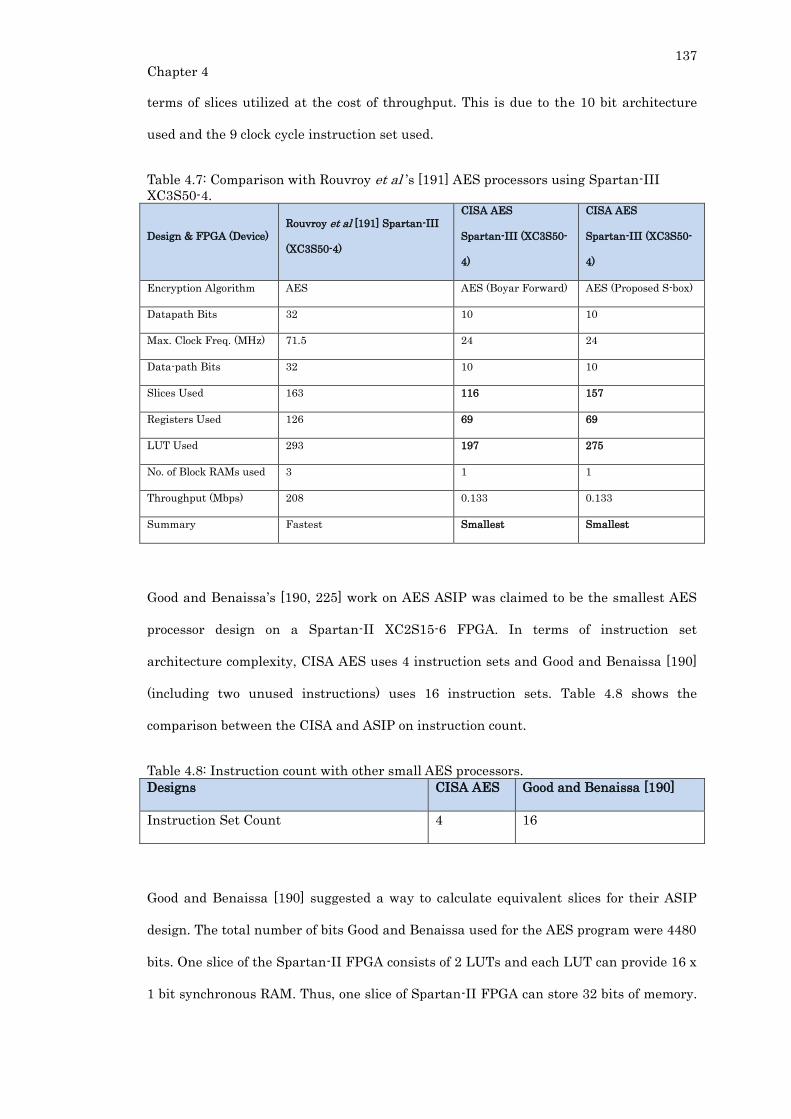
137
Chapter 4
terms of slices utilized at the cost of throughput. This is due to the 10 bit architecture
used and the 9 clock cycle instruction set used.
Table 4.7: Comparison with Rouvroy et al ’s [191] AES processors using Spartan-III
XC3S50-4.
Design & FPGA (Device)
Rouvroy et al [191] Spartan-III
(XC3S50-4)
CISA AES
Spartan-III (XC3S50-
4)
CISA AES
Spartan-III (XC3S50-
4)
Encryption Algorithm AES AES (Boyar Forward) AES (Proposed S-box)
Datapath Bits 32 10 10
Max. Clock Freq. (MHz) 71.5 24 24
Data-path Bits 32 10 10
Slices Used 163 116 157
Registers Used 126 69 69
LUT Used 293 197 275
No. of Block RAMs used 3 1 1
Throughput (Mbps) 208 0.133 0.133
Summary Fastest Smallest Smallest
Good and Benaissa’s [190, 225] work on AES ASIP was claimed to be the smallest AES
processor design on a Spartan-II XC2S15-6 FPGA. In terms of instruction set
architecture complexity, CISA AES uses 4 instruction sets and Good and Benaissa [190]
(including two unused instructions) uses 16 instruction sets. Table 4.8 shows the
comparison between the CISA and ASIP on instruction count.
Table 4.8: Instruction count with other small AES processors.
Designs CISA AES Good and Benaissa [190]
Instruction Set Count 4 16
Good and Benaissa [190] suggested a way to calculate equivalent slices for their ASIP
design. The total number of bits Good and Benaissa used for the AES program were 4480
bits. One slice of the Spartan-II FPGA consists of 2 LUTs and each LUT can provide 16 x
1 bit synchronous RAM. Thus, one slice of Spartan-II FPGA can store 32 bits of memory.
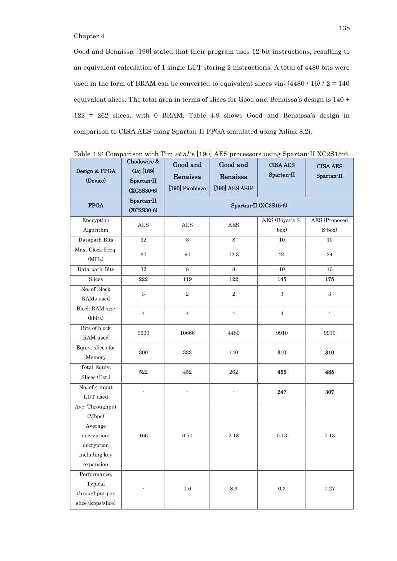
138
Chapter 4
Good and Benaissa [190] stated that their program uses 12 bit instructions, resulting to
an equivalent calculation of 1 single LUT storing 2 instructions. A total of 4480 bits were
used in the form of BRAM can be converted to equivalent slices via: (4480 / 16) / 2 = 140
equivalent slices. The total area in terms of slices for Good and Benaissa’s design is 140 +
122 = 262 slices, with 0 BRAM. Table 4.9 shows Good and Benaissa’s design in
comparison to CISA AES using Spartan-II FPGA simulated using Xilinx 8.2i.
Table 4.9: Comparison with Tim et al ‘s [190] AES processors using Spartan-II XC2S15-6.
Design & FPGA
(Device)
Chodowiec &
Gaj [189]
Spartan-II
(XC2S30-6)
Good and
Benaissa
[190] Picoblaze
Good and
Benaissa
[190] AES ASIP
CISA AES
Spartan-II
CISA AES
Spartan-II
FPGA Spartan-II
(XC2S30-6) Spartan-II (XC2S15-6)
Encryption
Algorithm AES AES AES
AES (Boyar’s S-
box)
AES (Proposed
S-box)
Datapath Bits 32 8 8 10 10
Max. Clock Freq.
(MHz) 60 90 72.3 24 24
Data-path Bits 32 8 8 10 10
Slices 222 119 122 145 175
No. of Block
RAMs used 3 2 2 3 3
Block RAM size
(kbits) 4 4 4 4 4
Bits of block
RAM used 9600 10666 4480 9910 9910
Equiv. slices for
Memory 300 333 140 310 310
Total Equiv.
Slices (Est.) 522 452 262 455 485
No. of 4 input
LUT used - - - 247 307
Ave. Throughput
(Mbps)
Average
encryption-
decryption
including key
expansion
166 0.71 2.18 0.13 0.13
Performance,
Typical
throughput per
slice (kbps/slice)
- 1.6 8.3 0.3 0.27

139
Chapter 4
Design & FPGA
(Device)
Chodowiec &
Gaj [189]
Spartan-II
(XC2S30-6)
Good and
Benaissa
[190] Picoblaze
Good and
Benaissa
[190] AES ASIP
CISA AES
Spartan-II
CISA AES
Spartan-II
FPGA Spartan-II
(XC2S30-6) Spartan-II (XC2S15-6)
Summary Large area,
high speed Software based
Smallest 8 bit
architecture
Smallest 10 bit
architecture
Smallest 10 bit
architecture
The CISA AES is not the smaller design compared the Good and Benaissa’s [190] ASIP.
Good and Benaissa’s ASIP has an advantage of using a very simple processing core that
performs primitive operations such as moving 8-bit data, finite-field multiply by 2 (ffm2),
finite-field division by 2 (ffd2) and XOR. The primitive operations used in ASIP AES are
great in reducing computation complexity considering that ASIP AES only runs AES.
The ASIP primitive finite-field operations are highly specific to AES. Hardware
implementation of ffm2 and ffd2 are static logic, which defines the instruction set
architecture. The CISA is expected to be smaller than 32 bit architectures because of the
register size. Good and Benaissa’s ASIP has the better results in terms of area but CISA
has the flexibility to operate other programs due to its Turing-Complete nature and not
highly specific to only a single cipher. The CISA is also expected to utilize more memory
for the program because of the URISC’s nature for larger program memory.
4.3.7. Comparison with Other Small S-boxes
To compare S-box implementations, the S-box by Boyar et al [212] is chosen to be a
benchmark as it is the smallest known S-box. The total gate count for the Boyar et al ‘s
S-box is 115 gates. The comparisons with different S-boxes and the comparison of gate
counts are shown in Table 4.10.
Table 4.10: The comparison of different S-boxes. Basis Type XOR XNOR NAND / AND NOT MUX Total Gates
Proposed CISA AES S-Box
(bi-directional)
Merged 107 4 32 - 16 159
- - - - - - -
- - - - - - -

140
Chapter 4
Basis Type XOR XNOR NAND / AND NOT MUX Total Gates
- - - - - - -
- - - - - - -
Boyar [212] (Forward S-box)
- - - - - - -
S-box 79 4 32 - - 115
- - - - - - -
Boyar [71]
(Complete, bi-directional)
Merged 144 14 34 - 16 208
S-box 90 4 34 - - 128
Inv S-box 83 10 34 - - 127
Edwin [92]
(schematic gate count)
Merged 217 - 45 - 16 279
S-box 193 - 45 - - 238
Inv S-box 177 - 45 - - 222
Canright [69]
Merged 107 0 36 2 16 253
S-box 91 0 36 0 0 195
Inv S-box 91 0 36 0 0 195
Mentens [214]
Merged 118 0 36 0 16 271
S-box 96 0 36 0 0 204
Inv S-box 97 0 36 0 0 206
Satoh [68]
Merged 119 0 36 3 16 275
S-box 100 0 36 0 0 211
Inv S-box 99 0 36 0 0 209
Worst
Merged 131 0 36 0 16 293
S-box 107 0 36 0 0 223
Inv S-box 106 0 36 0 0 222
Assuming a multiplexer cost eight gates, the proposed S-box configuration uses 2 MUXes,
which costs 16 gates total. Canright [69] assumes an 8-bit MUX is equivalent to 8 gates
hence 16 gates is used in the calculations for the total gate count [69]. The proposed S-
box configurations had shown gate count improvement in the merge category. Merged S-
box is more popular in designing an RCE system that performs both on-node encryption
and decryption. A forward S-box has smaller gate count and an encryption-only program
can reduce the amount of logic and memory required when only encryption is required
on-node.
141
Chapter 4
4.4. Summary
In this chapter, an improved S-box with lower gate count, implemented together with a
low-complexity CISA AES processor is presented.
To summarize, this chapter presents the following:
1) TISC is used as the basic platform for CISA AES application.
2) Novel S-Box improvement (smaller gate-count than existing work is presented).
3) Minimization of the inverse affine circuit, from 24 gates to 14 gates.
4) CISA AES using Boyar’s forward S-box utilizing 116 slices using Spartan3
XCS1500L-4 FPGA.
5) CISA AES using the proposed bi-directional S-box utilizing 157 slices using
Spartan3 XCS1500L-4 FPGA.
.
142
Chapter 5
CHAPTER 5
LOW-COMPLEXITY MULTI-CIPHER CRYPTO-PROCESSOR
ARCHITECTURE FOR VISUAL SENSOR RESOURCE
CONSTRAINED ENVIRONMENTS – A NOVEL SOLUTION
__________________________________________________________________________________
5.1. The Proposed Multi-level, Multi-cipher Architecture (MMA)
The proposed MMA is a global architecture that utilizes the features of TISC Skipjack
and CISA AES, creating a system that allows multiple ciphers to co-exist within the
same crypto-system. The instruction sets for TISC Skipjack are sub-set of the CISA AES
instruction sets. Therefore, the TISC Skipjack and CISA AES share the same ALU (or
crypto-blocks). A single CISA AES processor can operate both Skipjack and AES because
both ciphers can be operated within the same CISA framework. In the context of a
crypto-processor, hardware accelerated ciphers are treated as ‘crypto-cores’. Hence TISC
Skipjack, CISA AES, or CISA in general are treated as ‘crypto-cores’ within the same
context.
Figure 5.1 shows the MMA dual crypto-processor block design with reconfigurable data
path around the cores. Two models of MMA are proposed. The first model is a multi-
cipher configuration with the coupling of a CISA Skipjack core and a CISA AES core,
forming the multi cipher architecture (MCA). The second model consists of two
independent AES processors and is referred to as the NAES in this thesis.
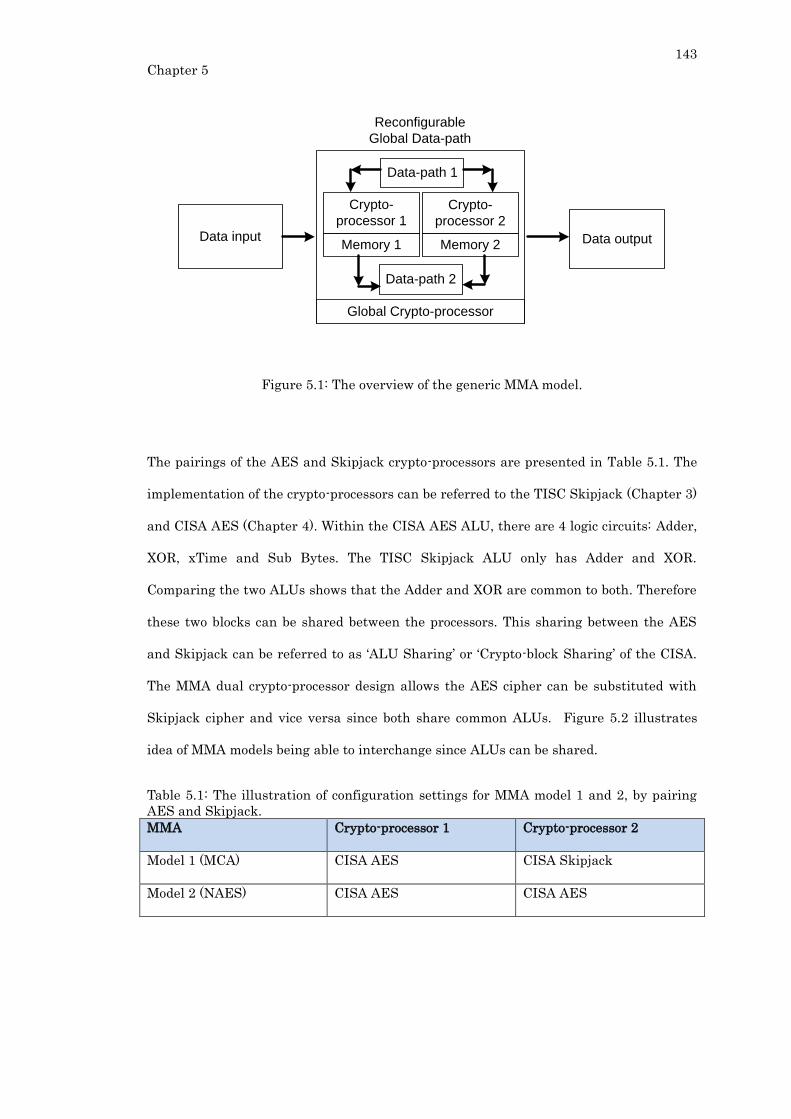
143
Chapter 5
Data input
Global Crypto-processor
Crypto-
processor 1
Crypto-
processor 2
Data output
Reconfigurable
Global Data-path
Memory 1 Memory 2
Data-path 1
Data-path 2
Figure 5.1: The overview of the generic MMA model.
The pairings of the AES and Skipjack crypto-processors are presented in Table 5.1. The
implementation of the crypto-processors can be referred to the TISC Skipjack (Chapter 3)
and CISA AES (Chapter 4). Within the CISA AES ALU, there are 4 logic circuits: Adder,
XOR, xTime and Sub Bytes. The TISC Skipjack ALU only has Adder and XOR.
Comparing the two ALUs shows that the Adder and XOR are common to both. Therefore
these two blocks can be shared between the processors. This sharing between the AES
and Skipjack can be referred to as ‘ALU Sharing’ or ‘Crypto-block Sharing’ of the CISA.
The MMA dual crypto-processor design allows the AES cipher can be substituted with
Skipjack cipher and vice versa since both share common ALUs. Figure 5.2 illustrates
idea of MMA models being able to interchange since ALUs can be shared.
Table 5.1: The illustration of configuration settings for MMA model 1 and 2, by pairing
AES and Skipjack.
MMA Crypto-processor 1 Crypto-processor 2
Model 1 (MCA) CISA AES CISA Skipjack
Model 2 (NAES) CISA AES CISA AES
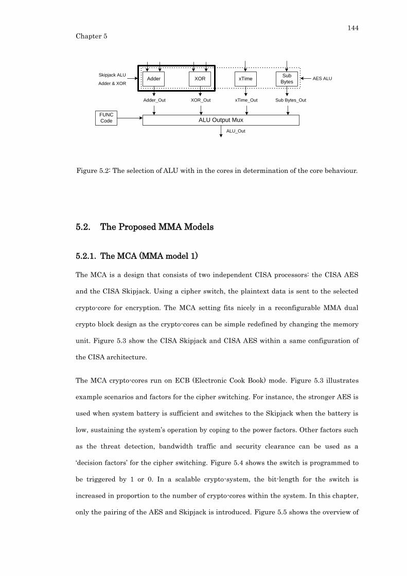
144
Chapter 5
xTime
xTime_Out
XOR
XOR_Out
Sub
Bytes
Sub Bytes_Out
Adder
Adder_Out
FUNC
Code ALU Output Mux
ALU_Out
Skipjack ALU
Adder & XORAES ALU
Figure 5.2: The selection of ALU with in the cores in determination of the core behaviour.
5.2. The Proposed MMA Models
5.2.1. The MCA (MMA model 1)
The MCA is a design that consists of two independent CISA processors: the CISA AES
and the CISA Skipjack. Using a cipher switch, the plaintext data is sent to the selected
crypto-core for encryption. The MCA setting fits nicely in a reconfigurable MMA dual
crypto block design as the crypto-cores can be simple redefined by changing the memory
unit. Figure 5.3 show the CISA Skipjack and CISA AES within a same configuration of
the CISA architecture.
The MCA crypto-cores run on ECB (Electronic Cook Book) mode. Figure 5.3 illustrates
example scenarios and factors for the cipher switching. For instance, the stronger AES is
used when system battery is sufficient and switches to the Skipjack when the battery is
low, sustaining the system’s operation by coping to the power factors. Other factors such
as the threat detection, bandwidth traffic and security clearance can be used as a
‘decision factors’ for the cipher switching. Figure 5.4 shows the switch is programmed to
be triggered by 1 or 0. In a scalable crypto-system, the bit-length for the switch is
increased in proportion to the number of crypto-cores within the system. In this chapter,
only the pairing of the AES and Skipjack is introduced. Figure 5.5 shows the overview of
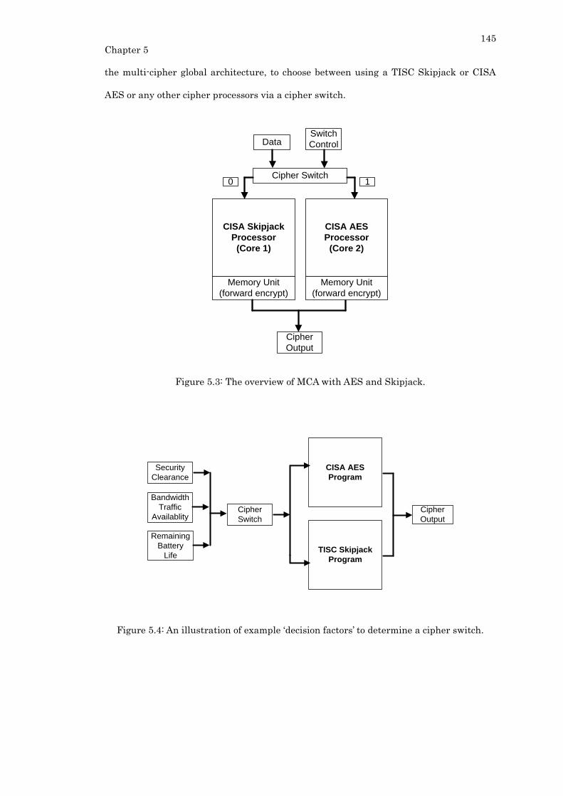
145
Chapter 5
the multi-cipher global architecture, to choose between using a TISC Skipjack or CISA
AES or any other cipher processors via a cipher switch.
Memory Unit
(forward encrypt)
CISA Skipjack
Processor
(Core 1)
Memory Unit
(forward encrypt)
CISA AES
Processor
(Core 2)
Cipher Switch
Cipher
Output
DataSwitch
Control
0 1
Figure 5.3: The overview of MCA with AES and Skipjack.
TISC Skipjack
Program
CISA AES
Program
Cipher
Output
Cipher
Switch
Security
Clearance
Bandwidth
Traffic
Availablity
Remaining
Battery
Life
Figure 5.4: An illustration of example ‘decision factors’ to determine a cipher switch.
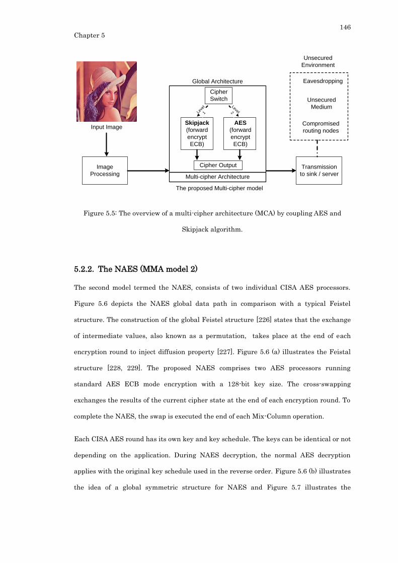
146
Chapter 5
Image
Processing
Input Image
Transmission
to sink / server
Unsecured
Medium
Compromised
routing nodes
Eavesdropping
Unsecured
Environment
Global Architecture
AES
(forward
encrypt
ECB)
Skipjack
(forward
encrypt
ECB)
Cipher Output
Level 2Leve
l
1
Cipher
Switch
The proposed Multi-cipher model
Multi-cipher Architecture
Figure 5.5: The overview of a multi-cipher architecture (MCA) by coupling AES and
Skipjack algorithm.
5.2.2. The NAES (MMA model 2)
The second model termed the NAES, consists of two individual CISA AES processors.
Figure 5.6 depicts the NAES global data path in comparison with a typical Feistel
structure. The construction of the global Feistel structure [226] states that the exchange
of intermediate values, also known as a permutation, takes place at the end of each
encryption round to inject diffusion property [227]. Figure 5.6 (a) illustrates the Feistal
structure [228, 229]. The proposed NAES comprises two AES processors running
standard AES ECB mode encryption with a 128-bit key size. The cross-swapping
exchanges the results of the current cipher state at the end of each encryption round. To
complete the NAES, the swap is executed the end of each Mix-Column operation.
Each CISA AES round has its own key and key schedule. The keys can be identical or not
depending on the application. During NAES decryption, the normal AES decryption
applies with the original key schedule used in the reverse order. Figure 5.6 (b) illustrates
the idea of a global symmetric structure for NAES and Figure 5.7 illustrates the
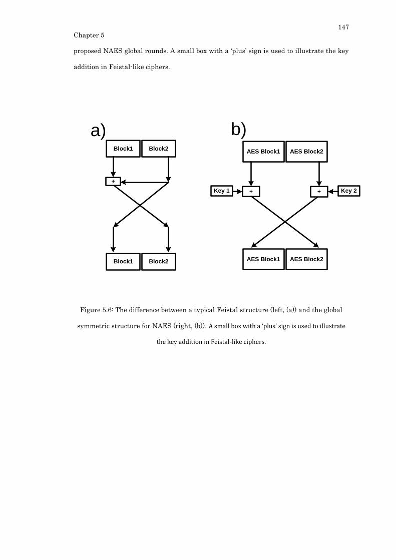
147
Chapter 5
proposed NAES global rounds. A small box with a ‘plus’ sign is used to illustrate the key
addition in Feistal-like ciphers.
Block1 Block2
Block1 Block2
+
a)AES Block1 AES Block2
AES Block1 AES Block2
+ +
b)
Key 2Key 1
Figure 5.6: The difference between a typical Feistal structure (left, (a)) and the global
symmetric structure for NAES (right, (b)). A small box with a ‘plus’ sign is used to illustrate
the key addition in Feistal-like ciphers.

148
Chapter 5
Shift Rows
Sub Bytes
Mix Colums
Plain Text 1
Shift Rows
Sub Bytes
Mix Colums
Plain Text 2
Round Key 2 (0)Round Key 1 (0)
Round Key 2 (i)Round Key 1 (i)
Shift Rows
Sub Bytes
Mix Colums
Shift Rows
Sub Bytes
Mix Colums
Repeat for 9
rounds
Shift Rows
Sub Bytes
Round Key 2 (i)
Round Key 2
(Nr)
Cipher Text
Shift Rows
Sub Bytes
Round Key 1 (i)
Round Key 1
(Nr)
Cipher Text
Figure 5.7: The illustration of a NAES using two separate AES processors, cross-
swapping the ciphers at the end of each round17.
17 Figure published in: Kong, J. H., L.-M. Ang, et al. (2013). "Minimalist security and privacy
schemes based on enhanced AES for integrated WISP sensor networks." Int. J. Commun. Netw.
Distrib. Syst. 11(2): 214-232, Figure 4.

149
Chapter 5
In a standard AES round function, Sub-Bytes, Shift Rows and Mix Column are applied to
the cipher. While designing NAES, the involvement of two keys occurs when the
intermediate values are swapped at the end of a round. When two keys are involved in
the encryption, a single wrong key added will result to the failure to decrypt the cipher.
The cipher cross-swapping has to be symmetrical and both AES processors have to be
run concurrently. Parallel AES execution will ensure that both cipher states are in the
same round.
The Shift Rows, Sub-Bytes and Mix Column are byte oriented operations, there are no
limitations as when and where the cross-swapping should occurs. The only issue
regarding the cipher’s complete round functions is that the cross-swapping has to either
occur before or after a key is XOR into the cipher concurrently. This is to ensure that the
cipher is in the correct state. A wrong round key added will result to a total decryption
failure. Figure 5.7 shows two AES round functions executed in parallel and the ciphers
are exchanged at the end of every round functions.
Within the NAES, the independent cores are the made up of two CISA AES processors.
Both CISA AES processors are driven by independent controllers and have their own
memory units. The illustration of the NAES is shown in Figure 5.8. The Global PC acts
as the reset mechanism to drive the CISA AES processors to start to program at a
specific memory location, in order to run the AES to a complete 10 rounds. Figure 5.9
shows the overview of the global architecture with two AES processors as cores in a
system.
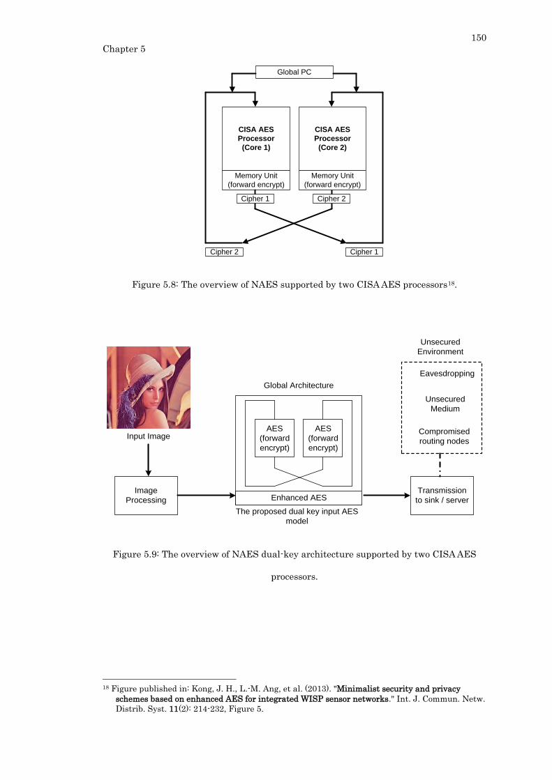
150
Chapter 5
Memory Unit
(forward encrypt)
CISA AES
Processor
(Core 1)
Memory Unit
(forward encrypt)
CISA AES
Processor
(Core 2)
Global PC
Cipher 1 Cipher 2
Cipher 1Cipher 2
Figure 5.8: The overview of NAES supported by two CISA AES processors18.
Image
Processing Enhanced AES
AES
(forward
encrypt)
AES
(forward
encrypt)
Input Image
Transmission
to sink / server
Unsecured
Medium
Compromised
routing nodes
Eavesdropping
The proposed dual key input AES
model
Unsecured
Environment
Global Architecture
Figure 5.9: The overview of NAES dual-key architecture supported by two CISA AES
processors.
18 Figure published in: Kong, J. H., L.-M. Ang, et al. (2013). "Minimalist security and privacy
schemes based on enhanced AES for integrated WISP sensor networks." Int. J. Commun. Netw.
Distrib. Syst. 11(2): 214-232, Figure 5.
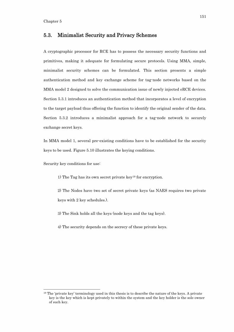
151
Chapter 5
5.3. Minimalist Security and Privacy Schemes
A cryptographic processor for RCE has to possess the necessary security functions and
primitives, making it adequate for formulating secure protocols. Using MMA, simple,
minimalist security schemes can be formulated. This section presents a simple
authentication method and key exchange scheme for tag-node networks based on the
MMA model 2 designed to solve the communication issue of newly injected eRCE devices.
Section 5.3.1 introduces an authentication method that incorporates a level of encryption
to the target payload thus offering the function to identify the original sender of the data.
Section 5.3.2 introduces a minimalist approach for a tag-node network to securely
exchange secret keys.
In MMA model 1, several pre-existing conditions have to be established for the security
keys to be used. Figure 5.10 illustrates the keying conditions.
Security key conditions for use:
1) The Tag has its own secret private key19 for encryption.
2) The Nodes have two set of secret private keys (as NAES requires two private
keys with 2 key schedules.).
3) The Sink holds all the keys (node keys and the tag keys).
4) The security depends on the secrecy of these private keys.
19 The ‘private key’ terminology used in this thesis is to describe the nature of the keys. A private
key is the key which is kept privately to within the system and the key holder is the sole owner
of such key.
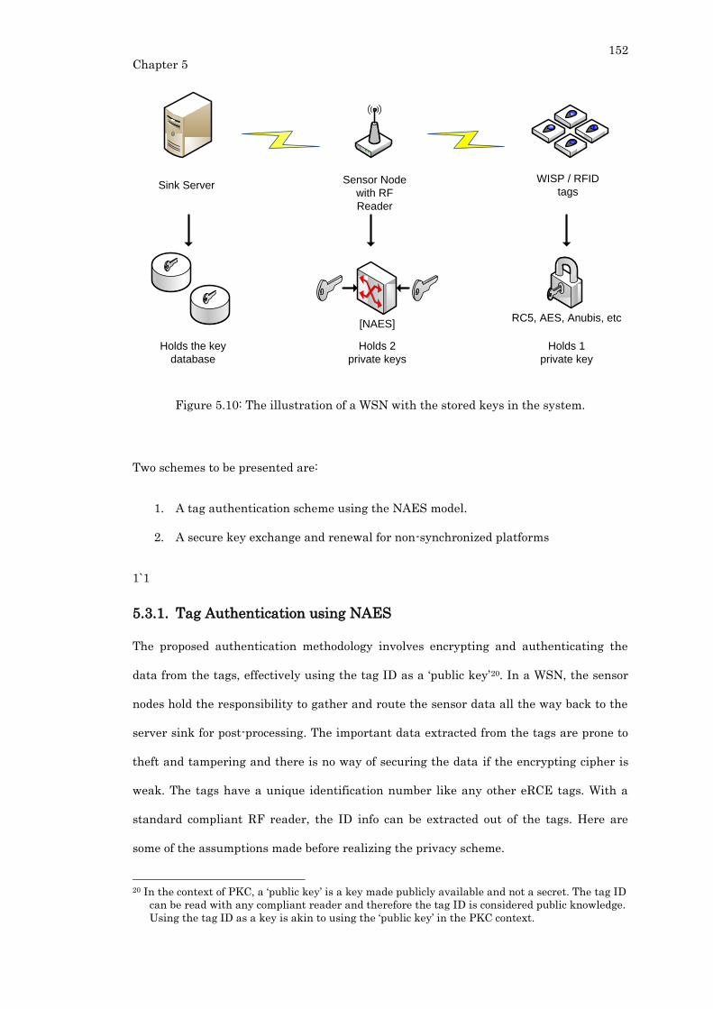
152
Chapter 5
Holds the key
database
Holds 2
private keys
Holds 1
private key
RC5, AES, Anubis, etc[NAES]
Sensor Node
with RF
Reader
Sink ServerWISP / RFID
tags
Figure 5.10: The illustration of a WSN with the stored keys in the system.
Two schemes to be presented are:
1. A tag authentication scheme using the NAES model.
2. A secure key exchange and renewal for non-synchronized platforms
1`1
5.3.1. Tag Authentication using NAES
The proposed authentication methodology involves encrypting and authenticating the
data from the tags, effectively using the tag ID as a ‘public key’20. In a WSN, the sensor
nodes hold the responsibility to gather and route the sensor data all the way back to the
server sink for post-processing. The important data extracted from the tags are prone to
theft and tampering and there is no way of securing the data if the encrypting cipher is
weak. The tags have a unique identification number like any other eRCE tags. With a
standard compliant RF reader, the ID info can be extracted out of the tags. Here are
some of the assumptions made before realizing the privacy scheme.
20 In the context of PKC, a ‘public key’ is a key made publicly available and not a secret. The tag ID
can be read with any compliant reader and therefore the tag ID is considered public knowledge.
Using the tag ID as a key is akin to using the ‘public key’ in the PKC context.

153
Chapter 5
Assumptions:
The tag ID is not a secret and can be extracted.
The tag is not clone-able, not forge-able and tags IDs are unique.
The tag has a pre-deployed encryption (block cipher) for secrecy.
The data transfer from tag to sensor node is assumed secured (no man-in-the-
middle attack).
In an environment where the sensor node has to monitor tens and hundreds of tags,
source identification is required to verify that from which source the data originated.
Since the data transferred from the tag to the node is assumed secured, then the next
step would be to digitally 'sign' the extracted data with the tag's ID. By using NAES, the
data encryption process takes in two key inputs: the node's private secret key and the
tag's ID. Figure 5.11 illustrates the proposed authentication process.
NAESData
(from
WISP)
Node’s Secret Key
- as Key 1
Tag ID
- as Key 2
Cipher-text
(signed and
encrypted with
Tag ID)NAES
Node’s Secret Key
- as Key 1
Tag ID
- as Key 2
Encryption
(Sensor Node)
Decryption
Sink (Server)
Data
(from
WISP)
Figure 5.11: The overview of the authentication process using NAES.
Figure 5.11 shows the authentication the encrypted data by decrypting it with the tag ID
as one of the keys. For a successful NAES decryption, both keys have to be correct. A
single wrong key will not result to the data decryption hence, the data is ‘signed’ with the
tag ID and protected with encryption. Even if the Tag ID can be easily extracted, the
decryption of the data is not possible because the NAES involves two keys. Verification

154
Chapter 5
of the data can be deduced from the correctness of the decrypted data. The preliminary
security analysis of the proposed authentication scheme will be discussed in the section
5.4.2.
5.3.2. Secure Key Exchange and Renewal
One of the biggest problems in symmetric encryption is key management. In order to
securely exchange secret keys, the system has to adopt the public key cryptography for
public key generation using the private key with complex computation. For secure
communication to take place, each party has to have the same encryption or decryption
key. Keys are usually transferred to the other party in a secure manner via some public
key encryption. But since the existing system is using a symmetric cipher primitive, the
PKC and block ciphers are not practical to coexist in the same system, weighing down
the system’s resources [228]. Shamir et al devised a protocol called the Three-Pass Key
Exchange Protocol [228, 230, 231]. The protocol is highly dependent on a commutative
cipher. A simple XOR is such a commutative cipher.
An XOR cipher is one in which the order of encryption and decryption is interchangeable,
just as the order of multiplication is interchangeable, for example: A * B * C = A * C * B
= C * B * A. In order to use this commutative cipher, an XOR block function has to be
provided by the computing engine. The ALUs in the CISA architecture consists of an
XOR block which is perfectly fine for the implementation. By using this XOR block, the
architecture is able to perform the XOR cryptography. Lightweight tags are capable of
executing XOR operations [141], so this is practically feasible for both RCE and eRCE.
For the key exchange to work, the key setup and the secure padlocking phase has to be
laid out. The proposed steps are shown below.
Key exchange steps:
1) The sink is to issue a new private key for the tag, namely Key X.

155
Chapter 5
2) The sensor node treats the Tag ID as a plaintext and encrypts it using the NAES,
with its 2 original secret private keys. The output of the encrypted Tag ID is
named the ‘session key 1’. (Key A)
3) On the tag’s side, the tag will use its private key to encrypt its own ID, resulting
‘session key 2’. (Key B)
4) By using XOR, the node XOR the key A with key X. (A * X)
5) The node sends it over to the tag, and the tag ‘XORs’ its key B to the product. (A *
X * B)
6) After sending it back to node will apply the XOR with Key A onto the product
again. (A * X * B) * A = X * B
7) And finally at the tag side, the tag XOR its Key B onto the product. (X * B) * B =
X
8) Therefore, X is securely transferred to the tag’s side.
With the steps above, the Key X is transferred to the tag’s side, the tag is able to update
its private key to this Key X, and therefore, key exchange is complete. Figure 5.12
illustrates the overall process of this padlocking.
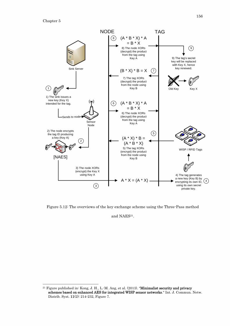
156
Chapter 5
Sink Server
Sensor
Node
WISP / RFID Tags
Sends to node
[NAES]
1) The sink issues a
new key (Key X)
intended for the tag.
2) The node encrypts
the tag ID producing
a key (Key A)
3) The node XORs
(encrypt) the Key X
using Key A
A * X = (A * X)
NODE TAG
(A * X) * B =
(A * B * X)5) The tag XORs
(encrypt) the product
from the node using
Key B
1
2
3
6
5
7
(A * B * X) * A
= B * X6) The node XORs
(decrypt) the product
from the tag using
Key A
(B * X) * B = X
7) The tag XORs
(decrypt) the product
from the node using
Key B
8 (A * B * X) * A
= B * X8) The node XORs
(decrypt) the product
from the tag using
Key A
4) The tag generates
a new key (Key B) by
encrypting its own ID,
using its own secret
private key.
4
9
Old Key Key X
9) The tag’s secret
key will be replaced
with Key X, hence
key renewed.
Figure 5.12: The overviews of the key exchange scheme using the Three-Pass method
and NAES21.
21 Figure published in: Kong, J. H., L.-M. Ang, et al. (2013). "Minimalist security and privacy
schemes based on enhanced AES for integrated WISP sensor networks." Int. J. Commun. Netw.
Distrib. Syst. 11(2): 214-232, Figure 7.
157
Chapter 5
5.4. Study and Analysis of NAES
5.4.1. Simulation Results for MMA model 1 (Effects on Images)
The effects of the proposed NAES direct encryption onto image data is simulated and
discussed in this section. JPEG images are encrypted directly as it is without additional
image processing in order to observe the perceptual degradation effect of NAES. The
dual-key dual channel NAES is simulated using the Matlab 2012a. An ideal cipher-image
histogram has to approximate the uniformly balanced distribution of cipher text values.
Each two adjacent encrypted pixels should be statistically non-correlated [232]. To test if
the NAES is able to encrypt highly-correlated images to produce uniform distributed
cipher texts, a sample image with dimensions of 512 by 512 pixels and in grayscale is
used. The data path scanning for both images are set to ‘ROW’ as in the encryption is
done row by row and via forward encryption ECB mode. Figure 5.13 shows the
comparison between NAES and AES encrypting an image directly using an image with a
fair amount of highly-correlated pixels. The effect of the encryption shows that both AES
and NAES perform similarly with an output of uniform distribution of cipher text. The
AES and NAES encrypted image shows acceptable perceptual confusion. Figure 5.14
shows the same experiment but with another scanning method. The effect of the
encryption with 4 by 4 block scanning shows both AES and NAES perform similarly with
an output of uniform distribution of cipher text.
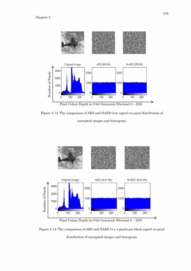
158
Chapter 5
Figure 5.13: The comparison of AES and NAES (row input) on pixel distribution of
encrypted images and histogram.
Figure 5.14: The comparison of AES and NAES (4 x 4 pixels per block input) on pixel
distribution of encrypted images and histogram.
Nu
mber
of
Pix
els
Nu
mber
of
Pix
els
Pixel Colour Depth in 8-bit Grayscale (Decimal 0 – 255)
Pixel Colour Depth in 8-bit Grayscale (Decimal 0 – 255)

159
Chapter 5
A portrait image with a simple and uniform background is used for the next experiment.
AES is known to perform poorly when encrypting image directly with highly correlated
neighbouring pixels. The results in Figure 5.15 showed improvement over the AES with
uniform distributed cipher text using NAES and also shows that the AES performs
poorly when encrypting an image that has a large amount of strong-correlated pixels.
Figure 5.16 shows the 4 x 4 block scanning encryption and the NAES shows slight
improvement over the AES. Figure 5.15 and Figure 5.16 shows that the AES encrypted
image has subtle imagery of certain pattern portraying a shape. The NAES shows that
improves in for both row and 4 by 4 scanning path.
Figure 5.15: The comparison of AES and NAES (row input) on pixel distribution of
encrypted images and histogram.
Nu
mber
of
Pix
els
Pixel Colour Depth in 8-bit Grayscale (Decimal 0 – 255)

160
Chapter 5
Figure 5.16: The comparison of AES and NAES (4 x 4 pixels per block input) on pixel
distribution of encrypted images and histogram.
Figure 5.17 shows the 4 by 4 ‘even and odd’ block path scanning methodology is used for
the experiment. The 4 by 4 ‘even and odd’ block path scanning method is method to sort
the image blocks into a 4 by 4 pixel blocks and labelling them with ‘1’, ‘2’, ‘3’ and etc.
subsequently and encrypt the block-pairs (even-odd pairing input to the NAES). This
method of scanning showed slight improvement over the normal 4 x 4 block scanning.
Figure 5.18 shows the comparison of AES, NAES and AES in cipher-block-chaining (CBC)
mode, which is a stream cipher mode. It is observed that the AES-CBC performs the best
for direct image encryption. The simulation results presented in the section shows that
the NAES is capable of performing perceptual image encryption and showed
improvements of direct AES encryption on image with high pixel correlation.
Nu
mber
of
Pix
els
Pixel Colour Depth in 8-bit Grayscale (Decimal 0 – 255)

161
Chapter 5
Figure 5.17: The comparison of NAES using even and odd block input.
Figure 5.18: The comparison of AES, NAES and AES-CBC.
Nu
mber
of
Pix
els
N
um
ber
of
Pix
els
Pixel Colour Depth in 8-bit Grayscale (Decimal 0 – 255)
Pixel Colour Depth in 8-bit Grayscale (Decimal 0 – 255)
162
Chapter 5
5.4.2. Discussions on NAES Security Issues
The NAES key schedule involves 2 different keys. If a set of NAES encrypted data is
divided into two for transmission via different route paths, the adversary will not be able
to decrypt the data with only half of the data set and 1 stolen key unless both the 2 keys
and 2 data parts are compromised. This further increases the complexity for the attacks.
The proposed authentication scheme is a technique that takes the advantage of providing
encryption and signing the data with the origin tag ID. By assuming that the private
keys are secured and secret, the adversary known the tag’s ID will not benefit the
attacks as the NAES architecture requires 2 keys for a complete decryption. The
proposed authentication scheme only benefits the sink server for verifying the origins of
this data set.
Menezes et al [228] stated the XOR cipher is vulnerable to the known-plaintext-attack.
The ‘plaintext’ in the context of NAES key exchange, is the new key distributed from the
sink server. The key is only known to the involved parties and there is no way that the
key will be known by any other parties prior to the successful key exchange. Hence, the
XOR cipher is secured.
For systems that require a Random Number Generator (RNG), the tag ID can be used.
Tag ID encrypted using both NAES private keys resulting to a random number
(encrypted ID) provided that the NAES private keys are replaced as this session.
Encrypting the Tag ID using the same private key pairs will result to the same value and
the random number will no longer be random after first generation. On the tag reader’s
side, the tag’s own ID can also be encrypted using its own private key, resulting to
another new random number (encrypted ID). This two sets of encrypted ID can be used a
“session” or “partner” keys, without the need for key assignment from network sink. This
is an alternative solution to creating random numbers without the need for dedicated
RNG. The partner keys from both sides are secured using their own respective private
keys unless the private keys of both sides are compromised. Vernam Cipher [228] stated
that a key used for encryption is safe if it is used for only once. In the case of renewing
163
Chapter 5
keys using NAES, the tag’s private key is only used for once in the events of key renewal
(XOR operation), after the new key is received, the old private key will be discarded. This
is a good solution for a quick key exchange when threat is suspected and the thus
providing difficulty for adversaries to access sensitive data as the data value drops over
time. To formulate meaningful schemes using NAES, the strength and secrecy of the
system relies heavily on the secrecy of the secret keys used, not the publicly-know Tag ID.
In a deployed RCE, a single compromised sensor device would lead to the whole
communication network exposed to adversaries. The simplest method of key distribution
is to pre-load a single common key or hard-code pre-defined keys to all the nodes before
they are deployed. This method does not require after-deployment key distribution
because they are capable of exchanging messages with that existing key but the major
drawback for this method is that, even a single compromised node would compromise the
security of the whole system. Another obvious method for a shared-key distribution
scheme is to pre-load distinct pair-wise key pairs in every node. This method poses
another major problem as it lacks scalability which RCE requires. The number of keys
that must be stored in each node is proportional to the total number of nodes in the
network. Since sensor nodes are resource constrained, this brings overhead which limits
the scheme’s applicability except for it can An alternative solution is to use key
management schemes. But a key management scheme would further increase the
systems’ processing load and communication delay. The proposed NAES is to use two
encryption blocks with two keys method and the keys are presumed to be pre-loaded into
the system without key distribution operations overhead. When a visual RCE device
processes an input image and attempts to send the vital information back to the sink, it
has to relay the information from node to node until it reaches the sink. When the data
reaches to a compromised node, the secrecy of the data would be revealed and hence the
security mechanism fails. Data re-routing is usually used to solve the issue [61] but with
the proposed method, compromised nodes will not hinder the transmission and
jeopardize the secured data. When an image is traditionally encrypted, blocks of bit
streams are usually the input for the cipher. When there are two ciphers used, two blocks
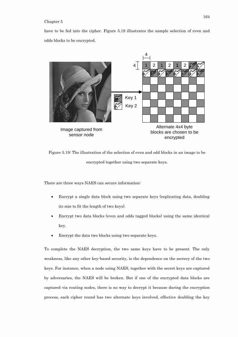
164
Chapter 5
have to be fed into the cipher. Figure 5.19 illustrates the sample selection of even and
odds blocks to be encrypted.
1
Image captured from
sensor node
4
4
Alternate 4x4 byte
blocks are chosen to be
encrypted
1 2 1 2 1 2
Key 2
Key 1
Figure 5.19: The illustration of the selection of even and odd blocks in an image to be
encrypted together using two separate keys.
There are three ways NAES can secure information:
Encrypt a single data block using two separate keys (replicating data, doubling
its size to fit the length of two keys).
Encrypt two data blocks (even and odds tagged blocks) using the same identical
key.
Encrypt the data two blocks using two separate keys.
To complete the NAES decryption, the two same keys have to be present. The only
weakness, like any other key-based security, is the dependence on the secrecy of the two
keys. For instance, when a node using NAES, together with the secret keys are captured
by adversaries, the NAES will be broken. But if one of the encrypted data blocks are
captured via routing nodes, there is no way to decrypt it because during the encryption
process, each cipher round has two alternate keys involved, effective doubling the key
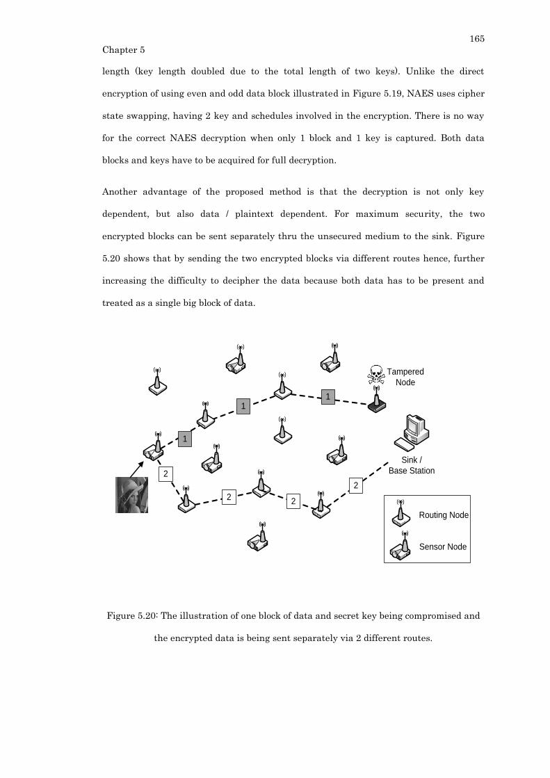
165
Chapter 5
length (key length doubled due to the total length of two keys). Unlike the direct
encryption of using even and odd data block illustrated in Figure 5.19, NAES uses cipher
state swapping, having 2 key and schedules involved in the encryption. There is no way
for the correct NAES decryption when only 1 block and 1 key is captured. Both data
blocks and keys have to be acquired for full decryption.
Another advantage of the proposed method is that the decryption is not only key
dependent, but also data / plaintext dependent. For maximum security, the two
encrypted blocks can be sent separately thru the unsecured medium to the sink. Figure
5.20 shows that by sending the two encrypted blocks via different routes hence, further
increasing the difficulty to decipher the data because both data has to be present and
treated as a single big block of data.
Routing Node
Sensor Node
Sink /
Base Station
1
11
2
2
2
2
Tampered
Node
Figure 5.20: The illustration of one block of data and secret key being compromised and
the encrypted data is being sent separately via 2 different routes.
166
Chapter 5
5.5. Summary
A novel unified architecture for multi-level security application, based on CISA
processors is presented. Two models: MCA and NAES are proposed as a solution to the
increasing security challenges of RCE application. These are the following features:
1) MMA model 1 can be used encrypt with variable security levels by choosing
crypto-primitives, depending on the application.
2) MMA model 1 is aimed to be scalable and only ALUs and program memories are
required for additional primitives.
3) MMA model 2 is a dual-channel cipher configuration that has shown direct image
encryption has improved perceptual degradation against normal AES.
4) The mirrored CISA cores in MMA have shown configurability to become model 2
with the help of instruction set programming and ALU sharing.
5) The proposed simple authentication and key exchange and renewal scheme is
based on the usage of CISA and uses the re-configurability of FPGA to offer these
simple schemes.
6) The proposed authentication method uses the Tag ID as a form of ‘public key’ and
the Tag ID is not a secret.
7) The proposed key exchange and renewal scheme, based on the Three-Pass
method, requires only XOR.
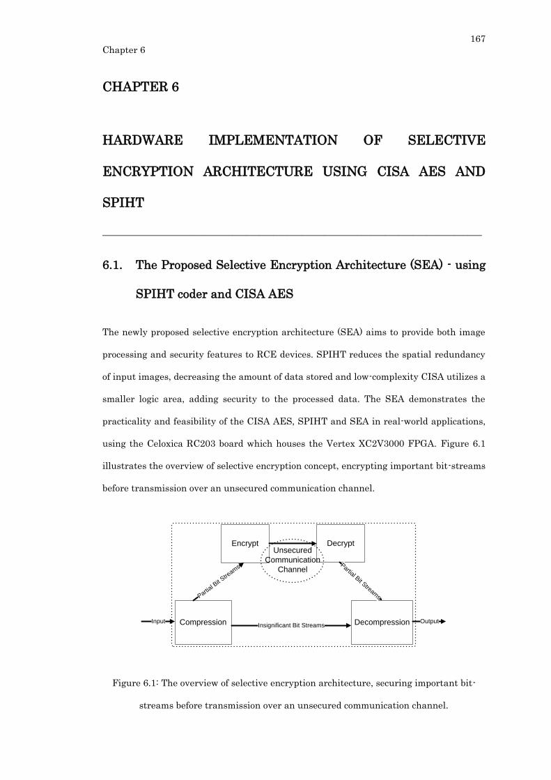
167
Chapter 6
CHAPTER 6
HARDWARE IMPLEMENTATION OF SELECTIVE
ENCRYPTION ARCHITECTURE USING CISA AES AND
SPIHT
__________________________________________________________________________________
6.1. The Proposed Selective Encryption Architecture (SEA) - using
SPIHT coder and CISA AES
The newly proposed selective encryption architecture (SEA) aims to provide both image
processing and security features to RCE devices. SPIHT reduces the spatial redundancy
of input images, decreasing the amount of data stored and low-complexity CISA utilizes a
smaller logic area, adding security to the processed data. The SEA demonstrates the
practicality and feasibility of the CISA AES, SPIHT and SEA in real-world applications,
using the Celoxica RC203 board which houses the Vertex XC2V3000 FPGA. Figure 6.1
illustrates the overview of selective encryption concept, encrypting important bit-streams
before transmission over an unsecured communication channel.
Compression
Partial B
it Stre
ams
Decompression
Encrypt
Insignificant Bit Streams
Decrypt
Partial Bit Streams
Unsecured
Communication
Channel
Input Output
Figure 6.1: The overview of selective encryption architecture, securing important bit-
streams before transmission over an unsecured communication channel.
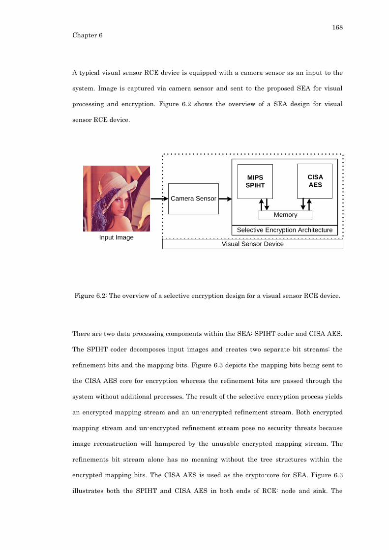
168
Chapter 6
A typical visual sensor RCE device is equipped with a camera sensor as an input to the
system. Image is captured via camera sensor and sent to the proposed SEA for visual
processing and encryption. Figure 6.2 shows the overview of a SEA design for visual
sensor RCE device.
Camera Sensor
Input Image
CISA
AESMIPS
SPIHT
Memory
Selective Encryption Architecture
Visual Sensor Device
Figure 6.2: The overview of a selective encryption design for a visual sensor RCE device.
There are two data processing components within the SEA: SPIHT coder and CISA AES.
The SPIHT coder decomposes input images and creates two separate bit streams: the
refinement bits and the mapping bits. Figure 6.3 depicts the mapping bits being sent to
the CISA AES core for encryption whereas the refinement bits are passed through the
system without additional processes. The result of the selective encryption process yields
an encrypted mapping stream and an un-encrypted refinement stream. Both encrypted
mapping stream and un-encrypted refinement stream pose no security threats because
image reconstruction will hampered by the unusable encrypted mapping stream. The
refinements bit stream alone has no meaning without the tree structures within the
encrypted mapping bits. The CISA AES is used as the crypto-core for SEA. Figure 6.3
illustrates both the SPIHT and CISA AES in both ends of RCE: node and sink. The
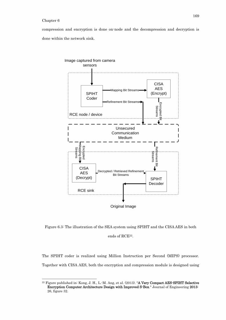
169
Chapter 6
compression and encryption is done on-node and the decompression and decryption is
done within the network sink.
SPIHT
Coder
CISA
AES
(Encrypt)
Image captured from camera
sensors
Refinement Bit Streams
Mapping Bit Streams
En
cry
pte
d B
it
Stre
am
s
Unsecured
Communication
Medium
SPIHT
Decoder
CISA
AES
(Decrypt)
Decrypted / Retrieved Refinement
Bit Streams
Re
fine
me
nt B
it
Stre
am
s
En
cry
pte
d
Ma
pp
ing
Bit
Stre
am
s
RCE sink
RCE node / device
Original Image
Figure 6.3: The illustration of the SEA system using SPIHT and the CISA AES in both
ends of RCE22.
The SPIHT coder is realized using Million Instruction per Second (MIPS) processor.
Together with CISA AES, both the encryption and compression module is designed using
22 Figure published in: Kong, J. H., L.-M. Ang, et al. (2013). "A Very Compact AES-SPIHT Selective
Encryption Computer Architecture Design with Improved S-Box." Journal of Engineering 2013:
26, figure 32.
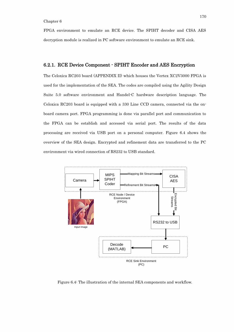
170
Chapter 6
FPGA environment to emulate an RCE device. The SPIHT decoder and CISA AES
decryption module is realized in PC software environment to emulate an RCE sink.
6.2.1. RCE Device Component - SPIHT Encoder and AES Encryption
The Celoxica RC203 board (APPENDIX II) which houses the Vertex XC2V3000 FPGA is
used for the implementation of the SEA. The codes are compiled using the Agility Design
Suite 5.0 software environment and Handel-C hardware description language. The
Celoxica RC203 board is equipped with a 330 Line CCD camera, connected via the on-
board camera port. FPGA programming is done via parallel port and communication to
the FPGA can be establish and accessed via serial port. The results of the data
processing are received via USB port on a personal computer. Figure 6.4 shows the
overview of the SEA design. Encrypted and refinement data are transferred to the PC
environment via wired connection of RS232 to USB standard.
MIPS
SPIHT
Coder
CISA
AESRefinement Bit Streams
Mapping Bit Streams
En
cry
pte
d B
it
Stre
am
s
RS232 to USB
PCDecode
(MATLAB)
RCE Sink Environment
(PC)
RCE Node / Device
Environment
(FPGA)
Camera
Input Image
Figure 6.4: The illustration of the internal SEA components and workflow.
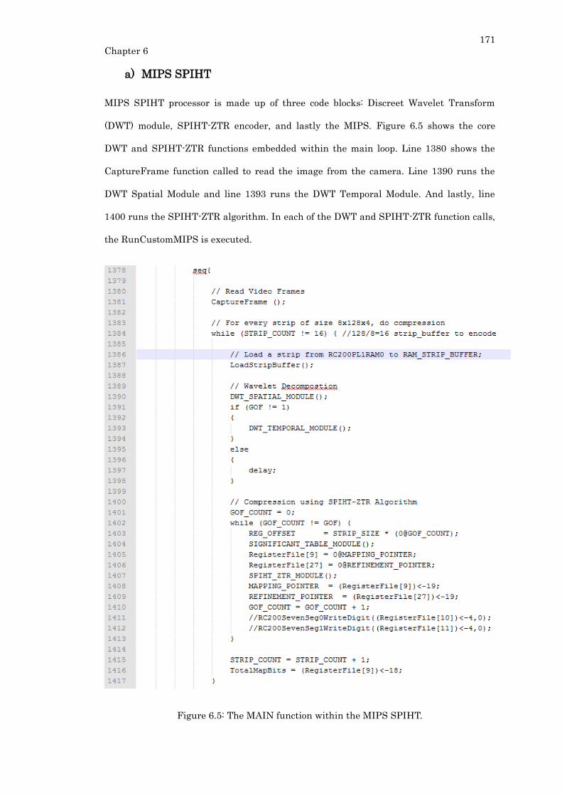
171
Chapter 6
a) MIPS SPIHT
MIPS SPIHT processor is made up of three code blocks: Discreet Wavelet Transform
(DWT) module, SPIHT-ZTR encoder, and lastly the MIPS. Figure 6.5 shows the core
DWT and SPIHT-ZTR functions embedded within the main loop. Line 1380 shows the
CaptureFrame function called to read the image from the camera. Line 1390 runs the
DWT Spatial Module and line 1393 runs the DWT Temporal Module. And lastly, line
1400 runs the SPIHT-ZTR algorithm. In each of the DWT and SPIHT-ZTR function calls,
the RunCustomMIPS is executed.
Figure 6.5: The MAIN function within the MIPS SPIHT.
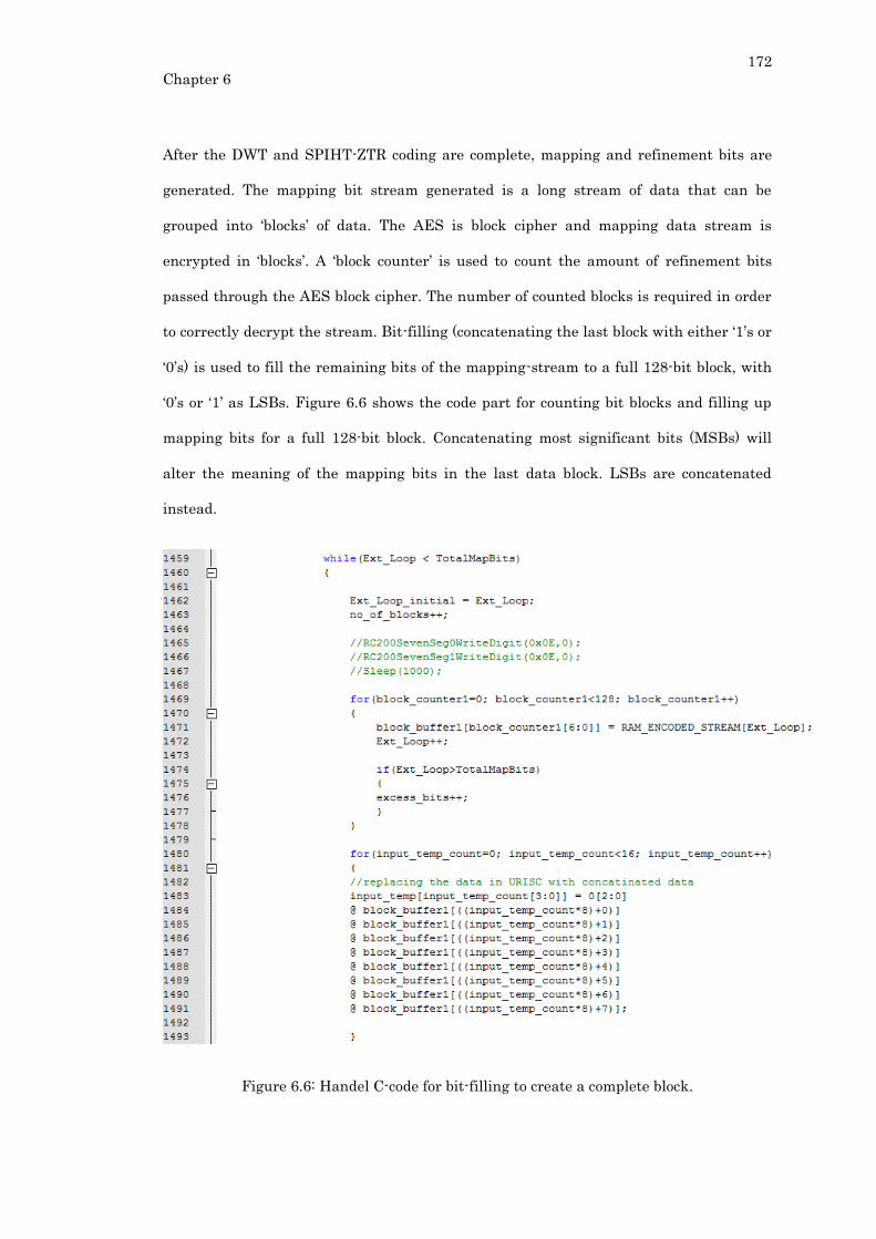
172
Chapter 6
After the DWT and SPIHT-ZTR coding are complete, mapping and refinement bits are
generated. The mapping bit stream generated is a long stream of data that can be
grouped into ‘blocks’ of data. The AES is block cipher and mapping data stream is
encrypted in ‘blocks’. A ‘block counter’ is used to count the amount of refinement bits
passed through the AES block cipher. The number of counted blocks is required in order
to correctly decrypt the stream. Bit-filling (concatenating the last block with either ‘1’s or
‘0’s) is used to fill the remaining bits of the mapping-stream to a full 128-bit block, with
‘0’s or ‘1’ as LSBs. Figure 6.6 shows the code part for counting bit blocks and filling up
mapping bits for a full 128-bit block. Concatenating most significant bits (MSBs) will
alter the meaning of the mapping bits in the last data block. LSBs are concatenated
instead.
Figure 6.6: Handel C-code for bit-filling to create a complete block.
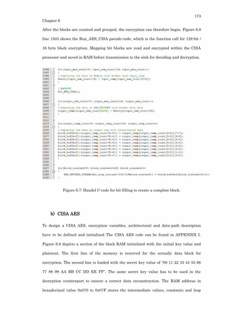
173
Chapter 6
After the blocks are counted and grouped, the encryption can therefore begin. Figure 6.8
line 1503 shows the Run_AES_CISA pseudo-code, which is the function call for 128-bit /
16 byte block encryption. Mapping bit blocks are read and encrypted within the CISA
processor and saved in RAM before transmission to the sink for decoding and decryption.
Figure 6.7: Handel C-code for bit-filling to create a complete block.
b) CISA AES
To design a CISA AES, encryption variables, architectural and data-path description
have to be defined and initialized The CISA AES code can be found in APPENDIX I.
Figure 6.8 depicts a section of the block RAM initialized with the initial key value and
plaintext. The first line of the memory is reserved for the actually data block for
encryption. The second line is loaded with the secret key value of “00 11 22 33 44 55 66
77 88 99 AA BB CC DD EE FF”. The same secret key value has to be used in the
decryption counterpart to ensure a correct data reconstruction. The RAM address in
hexadecimal value 0x070 to 0x07F stores the intermediate values, constants and loop
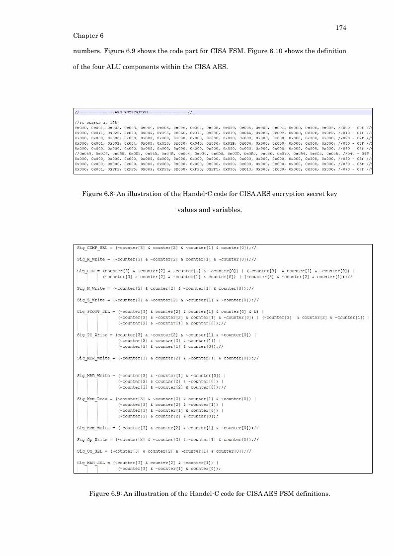
174
Chapter 6
numbers. Figure 6.9 shows the code part for CISA FSM. Figure 6.10 shows the definition
of the four ALU components within the CISA AES.
Figure 6.8: An illustration of the Handel-C code for CISA AES encryption secret key
values and variables.
Figure 6.9: An illustration of the Handel-C code for CISA AES FSM definitions.
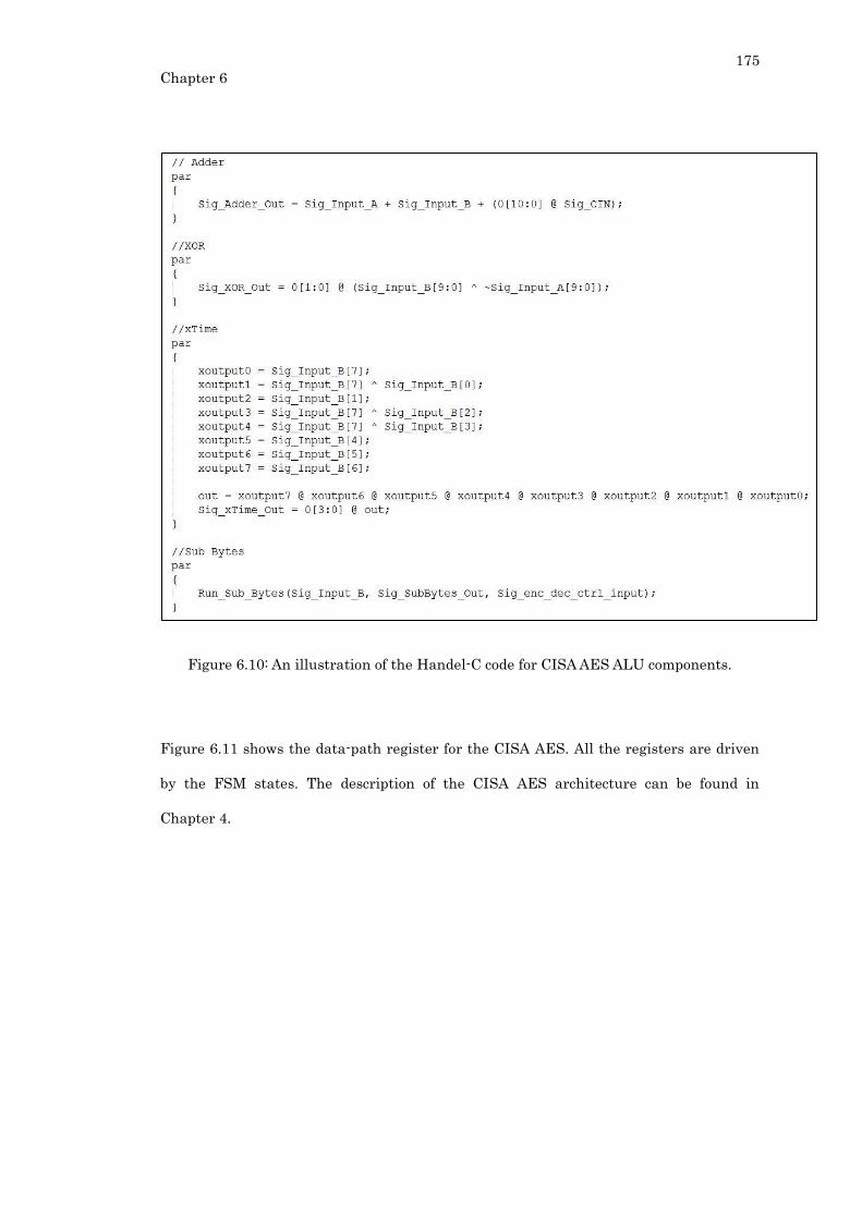
175
Chapter 6
Figure 6.10: An illustration of the Handel-C code for CISA AES ALU components.
Figure 6.11 shows the data-path register for the CISA AES. All the registers are driven
by the FSM states. The description of the CISA AES architecture can be found in
Chapter 4.
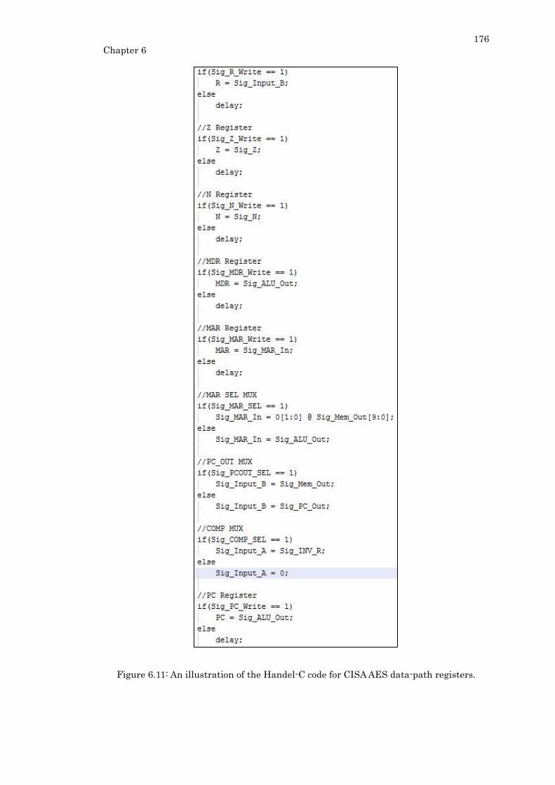
176
Chapter 6
Figure 6.11: An illustration of the Handel-C code for CISA AES data-path registers.
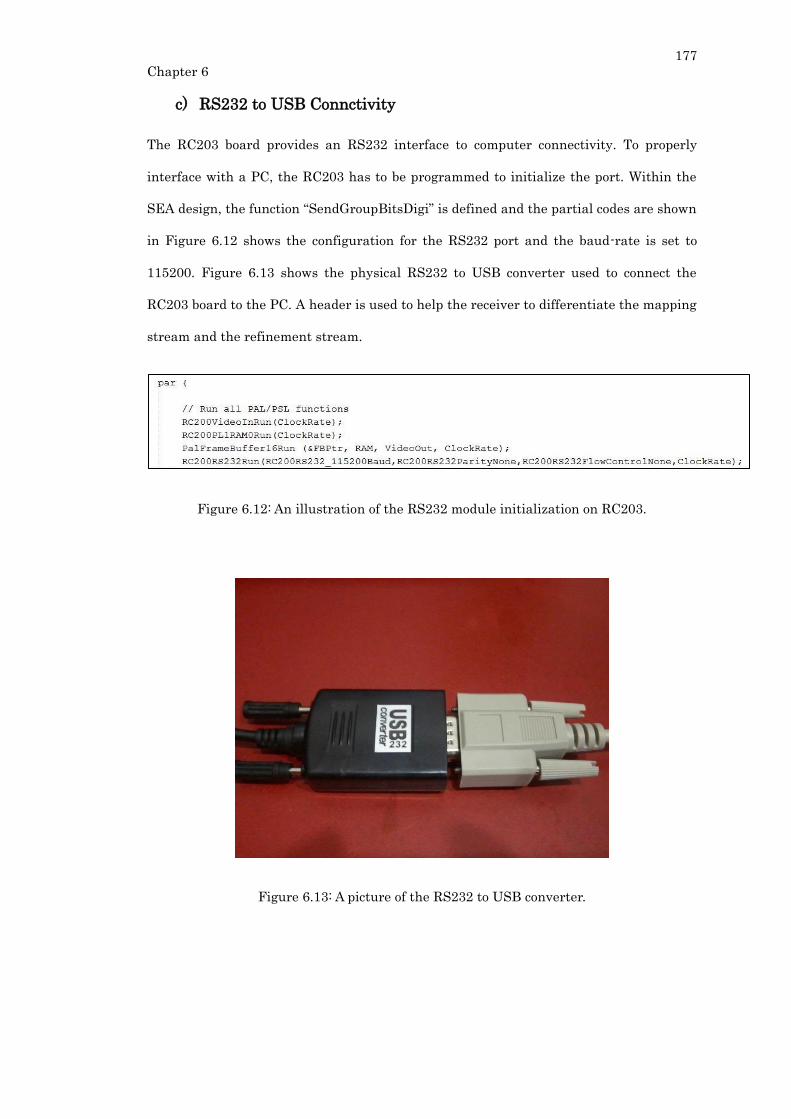
177
Chapter 6
c) RS232 to USB Connctivity
The RC203 board provides an RS232 interface to computer connectivity. To properly
interface with a PC, the RC203 has to be programmed to initialize the port. Within the
SEA design, the function “SendGroupBitsDigi” is defined and the partial codes are shown
in Figure 6.12 shows the configuration for the RS232 port and the baud-rate is set to
115200. Figure 6.13 shows the physical RS232 to USB converter used to connect the
RC203 board to the PC. A header is used to help the receiver to differentiate the mapping
stream and the refinement stream.
Figure 6.12: An illustration of the RS232 module initialization on RC203.
Figure 6.13: A picture of the RS232 to USB converter.
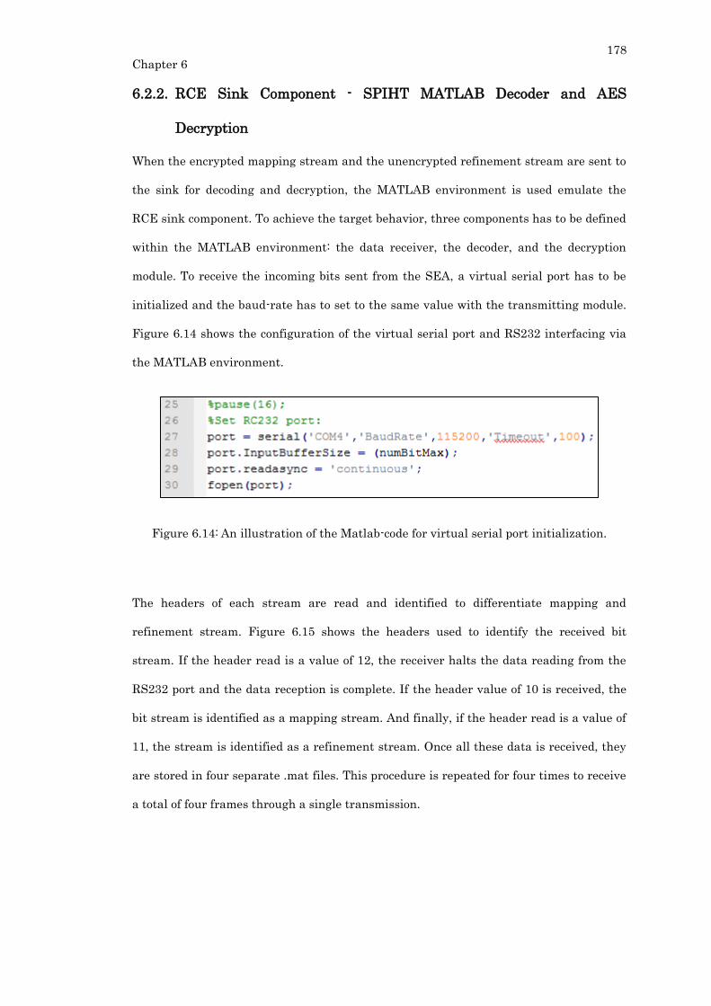
178
Chapter 6
6.2.2. RCE Sink Component - SPIHT MATLAB Decoder and AES
Decryption
When the encrypted mapping stream and the unencrypted refinement stream are sent to
the sink for decoding and decryption, the MATLAB environment is used emulate the
RCE sink component. To achieve the target behavior, three components has to be defined
within the MATLAB environment: the data receiver, the decoder, and the decryption
module. To receive the incoming bits sent from the SEA, a virtual serial port has to be
initialized and the baud-rate has to set to the same value with the transmitting module.
Figure 6.14 shows the configuration of the virtual serial port and RS232 interfacing via
the MATLAB environment.
Figure 6.14: An illustration of the Matlab-code for virtual serial port initialization.
The headers of each stream are read and identified to differentiate mapping and
refinement stream. Figure 6.15 shows the headers used to identify the received bit
stream. If the header read is a value of 12, the receiver halts the data reading from the
RS232 port and the data reception is complete. If the header value of 10 is received, the
bit stream is identified as a mapping stream. And finally, if the header read is a value of
11, the stream is identified as a refinement stream. Once all these data is received, they
are stored in four separate .mat files. This procedure is repeated for four times to receive
a total of four frames through a single transmission.
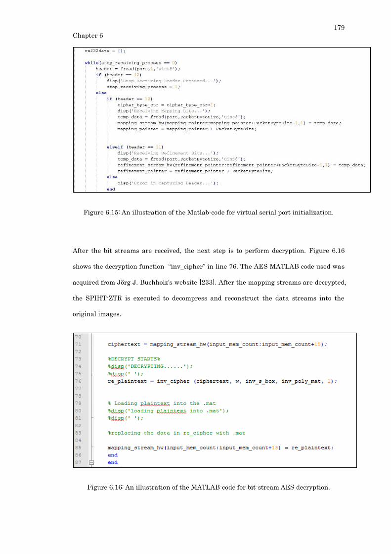
179
Chapter 6
Figure 6.15: An illustration of the Matlab-code for virtual serial port initialization.
After the bit streams are received, the next step is to perform decryption. Figure 6.16
shows the decryption function “inv_cipher” in line 76. The AES MATLAB code used was
acquired from Jörg J. Buchholz’s website [233]. After the mapping streams are decrypted,
the SPIHT-ZTR is executed to decompress and reconstruct the data streams into the
original images.
Figure 6.16: An illustration of the MATLAB-code for bit-stream AES decryption.
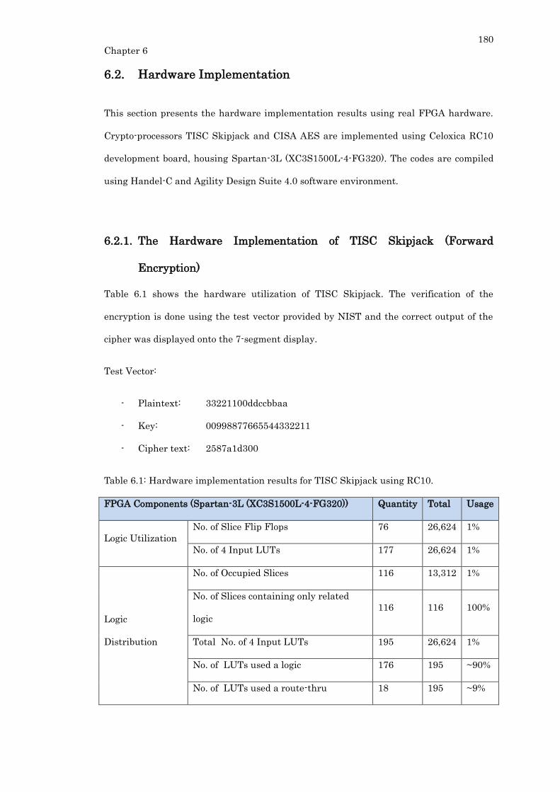
180
Chapter 6
6.2. Hardware Implementation
This section presents the hardware implementation results using real FPGA hardware.
Crypto-processors TISC Skipjack and CISA AES are implemented using Celoxica RC10
development board, housing Spartan-3L (XC3S1500L-4-FG320). The codes are compiled
using Handel-C and Agility Design Suite 4.0 software environment.
6.2.1. The Hardware Implementation of TISC Skipjack (Forward
Encryption)
Table 6.1 shows the hardware utilization of TISC Skipjack. The verification of the
encryption is done using the test vector provided by NIST and the correct output of the
cipher was displayed onto the 7-segment display.
Test Vector:
- Plaintext: 33221100ddccbbaa
- Key: 00998877665544332211
- Cipher text: 2587a1d300
Table 6.1: Hardware implementation results for TISC Skipjack using RC10.
FPGA Components (Spartan-3L (XC3S1500L-4-FG320)) Quantity Total Usage
Logic Utilization
No. of Slice Flip Flops 76 26,624 1%
No. of 4 Input LUTs 177 26,624 1%
Logic
Distribution
No. of Occupied Slices 116 13,312 1%
No. of Slices containing only related
logic
116 116 100%
Total No. of 4 Input LUTs 195 26,624 1%
No. of LUTs used a logic 176 195 ~90%
No. of LUTs used a route-thru 18 195 ~9%
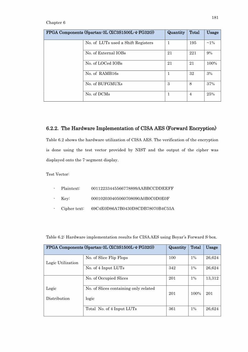
181
Chapter 6
FPGA Components (Spartan-3L (XC3S1500L-4-FG320)) Quantity Total Usage
No. of LUTs used a Shift Registers 1 195 ~1%
No. of External IOBs 21 221 9%
No. of LOCed IOBs 21 21 100%
No. of RAMB16s 1 32 3%
No. of BUFGMUXs 3 8 37%
No. of DCMs 1 4 25%
6.2.2. The Hardware Implementation of CISA AES (Forward Encryption)
Table 6.2 shows the hardware utilization of CISA AES. The verification of the encryption
is done using the test vector provided by NIST and the output of the cipher was
displayed onto the 7-segment display.
Test Vector:
- Plaintext: 00112233445566778899AABBCCDDEEFF
- Key: 000102030405060708090A0B0C0D0E0F
- Cipher text: 69C4E0D86A7B0430D8CDB78070B4C55A
Table 6.2: Hardware implementation results for CISA AES using Boyar’s Forward S-box.
FPGA Components (Spartan-3L (XC3S1500L-4-FG320)) Quantity Total Usage
Logic Utilization
No. of Slice Flip Flops 100 1% 26,624
No. of 4 Input LUTs 342 1% 26,624
Logic
Distribution
No. of Occupied Slices 201 1% 13,312
No. of Slices containing only related
logic
201 100% 201
Total No. of 4 Input LUTs 361 1% 26,624

182
Chapter 6
FPGA Components (Spartan-3L (XC3S1500L-4-FG320)) Quantity Total Usage
No. of LUTs used a logic 341 ~94% 361
No. of LUTs used a route-thru 19 ~6% 361
No. of LUTs used a Shift Registers 1 ~0% 361
No. of Bonded IOBs 28 12% 221
No. of LOCed IOBs 28 100% 28
No. of RAMB16s 1 3% 32
No. of BUFGMUXs 4 50% 8
No. of DCMs 1 25% 4
To validate the robustness of the CISA, 10 test vectors were used to test the design for
potential encryption errors. Table 6.3 shows the 10 test vectors used and the encrypted
texts are verified using “AES – Symmetric Cipher Online” [234].
Table 6.3: The 10 test vectors used to test the CISA AES and their respective cipher texts.
Plaintext Cipher text
Key = 00 10 20 30 40 50 60 70 80 90 A0 B0 C0 D0 E0 F0
00 11 22 33 44 55 66 77 88 99 AA BB CC
DD EE FF
30 34 AD CB A1 67 ED C3 87 16 4F 44 F0
95 50 F2
12 23 34 45 56 67 78 89 9A AB BC CD DE
EF F1 00
56 DA 6E 2B 62 FF D0 5E 1B 45 C7 8E FB
95 A7 77
00 11 99 22 88 33 77 44 66 55 AA FF BB
EE CC DD
D8 24 E7 D1 9C C7 13 AB 3F C1 24 B1 8B
81 76 D2
FF EE DD CC BB AA 99 88 77 66 55 44 33
22 11 00
2D 47 D1 48 4A 79 25 FE 2A D2 1A 42 3F
21 E5 0C
22 99 33 88 44 77 55 66 11 00 EE FF DD
CC AA BB
2D D9 C3 E3 BA 7D CF 0F B8 5C 4D B9 96
70 91 FB
66 77 88 99 22 33 44 55 11 00 AA EE FF
DD BB CC
40 0D F1 83 23 7C 8A 8B B7 FA 13 03 5E
84 D0 0B
12 21 34 43 56 65 78 87 90 09 AB BA CD
DC EF FE
29 C1 3F B0 C9 19 5F 06 D0 1A 09 D9 0A
58 AD C0
12 34 65 78 90 AB CD EF 12 34 65 78 90
AB CD EF
56 D6 F8 F0 F6 E2 5A EF 80 0E B1 59 CD
6F 07 E3
183
Chapter 6
Plaintext Cipher text
Key = 00 10 20 30 40 50 60 70 80 90 A0 B0 C0 D0 E0 F0
FE DC BA 98 76 54 32 10 FE DC BA 98 76
54 32 10
16 87 C5 28 12 76 04 3D AD F7 0B 7F 94
91 C6 F4
AF BD EA 46 81 68 41 88 12 34 89 75 24
90 88 99
15 67 DA 8E 48 F0 0E DC 08 A8 2B B8 F7
09 8C 9F
6.2.3. The Hardware Implementation of SEA
The Celoxica RC203 board which houses the Vertex XC2V3000 FPGA is used for the
implementation of the SEA. The codes are compiled using the Agility Design Suite 5.0
software environment and Handel-C hardware description language. A complete system
of selective encryption with a CISA AES processor working side-by-side with a MIPS
SPIHT coder is implemented. A still-portrait image is displayed on a HP 17 inches LCD
monitor is used as an image input to the video camera to the SPIHT AES setup. The SEA
design was powered up for 24 hours to capture live images and the images were
encrypted and decrypted without errors. Figure 6.17 depicts the experimental setup for
the proposed SEA.
Figure 6.17: The experimental setup for the development of SEA.

184
Chapter 6
Four 128 x 128 image frames are captured, encrypted on-board, and sent to another
computer for decryption. The CISA AES is programmed to encrypt only the mapping bits
and both mapping and refinement bits are sent out to the host computer once the
encryption has completed. The received bits are then processed in MATLAB environment
and the last 2 frames are chosen for decryption to verify the correct encryption and
decryption. Figure 6.18 shows the four images capture from the SEA. Note Figure 6.19
shows an example of the selective-encrypted on the Lena image, capture via the 330 line
CCD camera. From perceptual observation, the encrypted frames are unintelligible.
Figure 6.18: The four selectively encrypted frames with the last two frames decrypted.
Figure 6.19: Selective encryption on Lena image.
The logic utilization results for the complete SEA can be found in Table 6.4. The number
of slice flip-flops occupied is 3692 at 12% utilization. The number of 4 input LUTs
occupied are 8793 at 30% utilization. As for the logic distribution results, Table 6.5 shows
a total of 6251 slices occupied. As for the LUT utilization report, Table 6.6 shows a total
of 10176 4 input LUTs were used, at 35% utilization. Table 6.7 shows other FPGA
components utilized by the FPGA implementation of SEA.
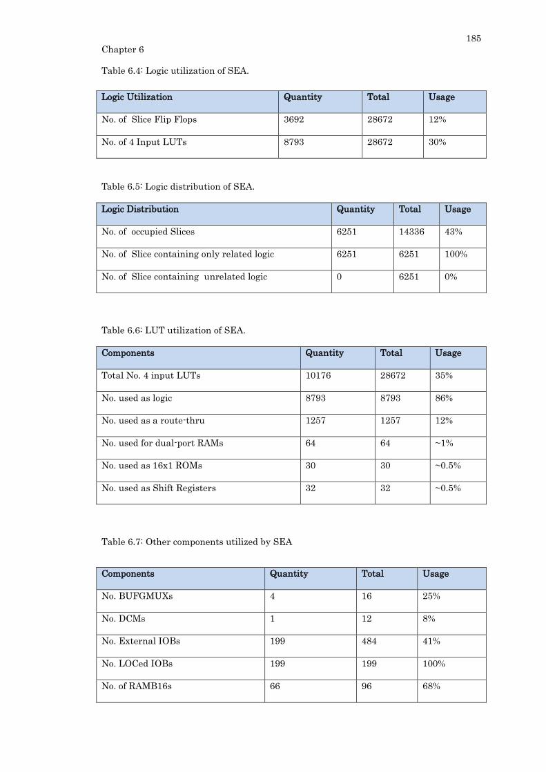
185
Chapter 6
Table 6.4: Logic utilization of SEA.
Logic Utilization Quantity Total Usage
No. of Slice Flip Flops 3692 28672 12%
No. of 4 Input LUTs 8793 28672 30%
Table 6.5: Logic distribution of SEA.
Logic Distribution Quantity Total Usage
No. of occupied Slices 6251 14336 43%
No. of Slice containing only related logic 6251 6251 100%
No. of Slice containing unrelated logic 0 6251 0%
Table 6.6: LUT utilization of SEA.
Components Quantity Total Usage
Total No. 4 input LUTs 10176 28672 35%
No. used as logic 8793 8793 86%
No. used as a route-thru 1257 1257 12%
No. used for dual-port RAMs 64 64 ~1%
No. used as 16x1 ROMs 30 30 ~0.5%
No. used as Shift Registers 32 32 ~0.5%
Table 6.7: Other components utilized by SEA
Components Quantity Total Usage
No. BUFGMUXs 4 16 25%
No. DCMs 1 12 8%
No. External IOBs 199 484 41%
No. LOCed IOBs 199 199 100%
No. of RAMB16s 66 96 68%

186
Chapter 7
CHAPTER 7
CONCLUSION
__________________________________________________________________________________
This thesis presents low-complexity, low-area cryptographic processors based on URISC.
RCE systems security requirements can be fulfilled using cryptographic primitives.
Cryptographic primitives suitable for RCE are concluded to be the AES and Skipjack. To
implement a low-complexity, low-area cryptographic processor for AES and Skipjack, the
Turing-Complete URISC is used as a foundation of the processor. By modifying the
URISC for cryptographic application, the low-complexity two instruction set computer
operating the full 64-bit Skipjack lightweight cipher is designed. The logic utilization for
TISC Skipjack on a Spartan-3L XC3S1500L-4-FG320 FPGA shows a total of 71 slices
occupied, 70 slice flip-flops and 94 4-input LUTs utilized. Using the TISC as a foundation,
the second design, CISA, operating the full 128-bit AES cipher is designed. The logic
utilization for TISC Skipjack on a Spartan-3L XC3S1500L-4-FG320 FPGA shows 157
slices occupied, 69 slice flip-flops and 275 4-input. The proposed AES S-box’s gate count
is decreased from Boyar’s [71] count of 208 to 159. The CISA AES is the smallest known
design FPGA compared to other designs on a Spartan-3 family FPGA.
The proposed TISC and CISA are rooted on a Turing-Complete architecture, which
allows them to be able to compute other arithmetic operations with additional
computation blocks. This feature enables the architecture to be scalable in a
reconfigurable environment. The behavior of the CISA depends on the program memory
loaded into the architecture. With multiple cipher programs loaded in CISA, the same
architecture is able to perform multiple ciphers. Unlike an ASIP which can only perform
a single specific task, a CISA can perform multiple ciphers in a single architecture with
the help of additional crypto-blocks. This feature is suitable for RCE applications to face
increasing security challenges by providing multiple security solutions in the form of
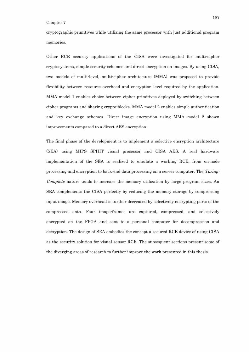
187
Chapter 7
cryptographic primitives while utilizing the same processor with just additional program
memories.
Other RCE security applications of the CISA were investigated for multi-cipher
cryptosystems, simple security schemes and direct encryption on images. By using CISA,
two models of multi-level, multi-cipher architecture (MMA) was proposed to provide
flexibility between resource overhead and encryption level required by the application.
MMA model 1 enables choice between cipher primitives deployed by switching between
cipher programs and sharing crypto-blocks. MMA model 2 enables simple authentication
and key exchange schemes. Direct image encryption using MMA model 2 shown
improvements compared to a direct AES encryption.
The final phase of the development is to implement a selective encryption architecture
(SEA) using MIPS SPIHT visual processor and CISA AES. A real hardware
implementation of the SEA is realized to emulate a working RCE, from on-node
processing and encryption to back-end data processing on a server computer. The Turing-
Complete nature tends to increase the memory utilization by large program sizes. An
SEA complements the CISA perfectly by reducing the memory storage by compressing
input image. Memory overhead is further decreased by selectively encrypting parts of the
compressed data. Four image-frames are captured, compressed, and selectively
encrypted on the FPGA and sent to a personal computer for decompression and
decryption. The design of SEA embodies the concept a secured RCE device of using CISA
as the security solution for visual sensor RCE. The subsequent sections present some of
the diverging areas of research to further improve the work presented in this thesis.
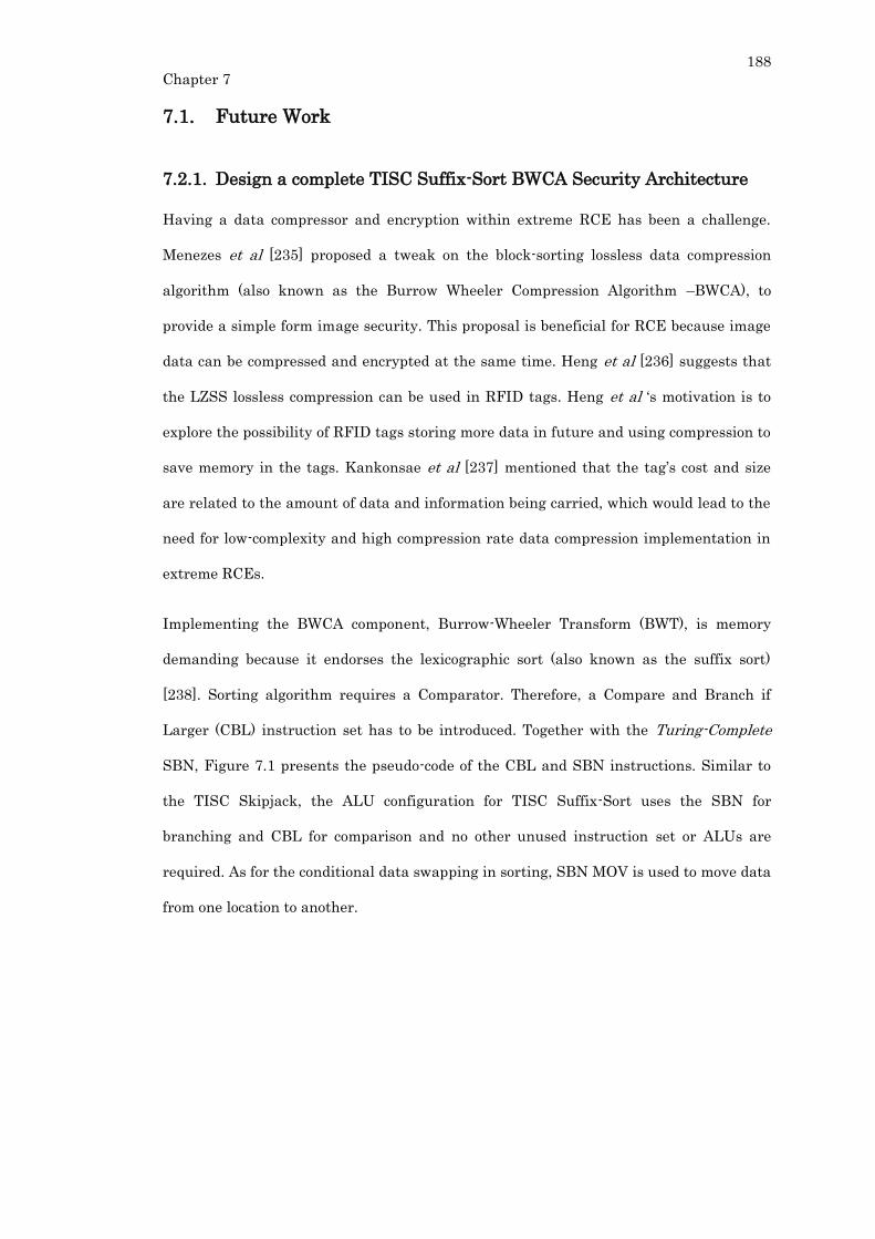
188
Chapter 7
7.1. Future Work
7.2.1. Design a complete TISC Suffix-Sort BWCA Security Architecture
Having a data compressor and encryption within extreme RCE has been a challenge.
Menezes et al [235] proposed a tweak on the block-sorting lossless data compression
algorithm (also known as the Burrow Wheeler Compression Algorithm –BWCA), to
provide a simple form image security. This proposal is beneficial for RCE because image
data can be compressed and encrypted at the same time. Heng et al [236] suggests that
the LZSS lossless compression can be used in RFID tags. Heng et al ‘s motivation is to
explore the possibility of RFID tags storing more data in future and using compression to
save memory in the tags. Kankonsae et al [237] mentioned that the tag’s cost and size
are related to the amount of data and information being carried, which would lead to the
need for low-complexity and high compression rate data compression implementation in
extreme RCEs.
Implementing the BWCA component, Burrow-Wheeler Transform (BWT), is memory
demanding because it endorses the lexicographic sort (also known as the suffix sort)
[238]. Sorting algorithm requires a Comparator. Therefore, a Compare and Branch if
Larger (CBL) instruction set has to be introduced. Together with the Turing-Complete
SBN, Figure 7.1 presents the pseudo-code of the CBL and SBN instructions. Similar to
the TISC Skipjack, the ALU configuration for TISC Suffix-Sort uses the SBN for
branching and CBL for comparison and no other unused instruction set or ALUs are
required. As for the conditional data swapping in sorting, SBN MOV is used to move data
from one location to another.
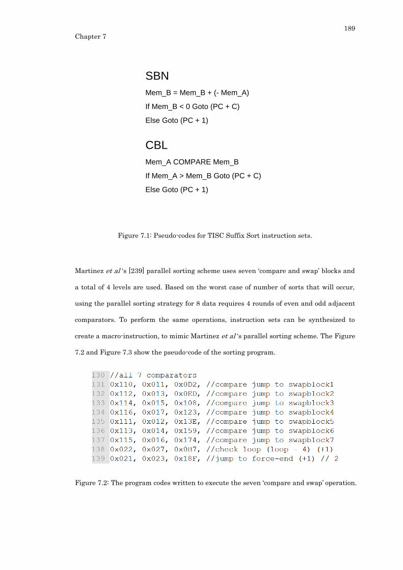
189
Chapter 7
SBN
Mem_B = Mem_B + (- Mem_A)
If Mem_B < 0 Goto (PC + C)
Else Goto (PC + 1)
CBL
Mem_A COMPARE Mem_B
If Mem_A > Mem_B Goto (PC + C)
Else Goto (PC + 1)
Figure 7.1: Pseudo-codes for TISC Suffix Sort instruction sets.
Martinez et al ‘s [239] parallel sorting scheme uses seven ‘compare and swap’ blocks and
a total of 4 levels are used. Based on the worst case of number of sorts that will occur,
using the parallel sorting strategy for 8 data requires 4 rounds of even and odd adjacent
comparators. To perform the same operations, instruction sets can be synthesized to
create a macro-instruction, to mimic Martinez et al ‘s parallel sorting scheme. The Figure
7.2 and Figure 7.3 show the pseudo-code of the sorting program.
Figure 7.2: The program codes written to execute the seven ‘compare and swap’ operation.
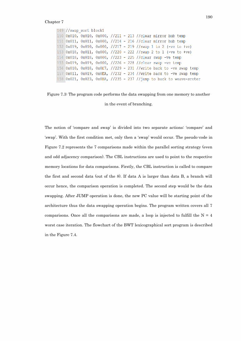
190
Chapter 7
Figure 7.3: The program code performs the data swapping from one memory to another
in the event of branching.
The notion of ‘compare and swap’ is divided into two separate actions: ‘compare’ and
‘swap’. With the first condition met, only then a ‘swap’ would occur. The pseudo-code in
Figure 7.2 represents the 7 comparisons made within the parallel sorting strategy (even
and odd adjacency comparison). The CBL instructions are used to point to the respective
memory locations for data comparisons. Firstly, the CBL instruction is called to compare
the first and second data (out of the 8). If data A is larger than data B, a branch will
occur hence, the comparison operation is completed. The second step would be the data
swapping. After JUMP operation is done, the new PC value will be starting point of the
architecture thus the data swapping operation begins. The program written covers all 7
comparisons. Once all the comparisons are made, a loop is injected to fulfill the N = 4
worst case iteration. The flowchart of the BWT lexicographical sort program is described
in the Figure 7.4.

191
Chapter 7
SWAP_1 (A1, A2)
SWAP_2 (A3, A4)
SWAP_3 (A5, A6)
SWAP_4 (A7, A8)
SWAP_5 (A2, A3)
SWAP_6 (A4, A5)
SWAP_7 (A6, A7)
A1 > A2 ?
A3 > A4 ?
A5 > A6 ?
A7 > A8 ?
A2 > A3 ?
A4 > A5 ?
A6 > A7 ?
Compare (A1, A2)
Compare (A3, A4)
Compare (A5, A6)
Compare (A7, A8)
Compare (A2, A3)
Compare (A4, A5)
Compare (A6, A7)
YES
YES
YES
YES
YES
YES
YES
NO
NO
NO
NO
NO
NO
LOOP = 4 ?
END
START
YES
NO
NO
Figure 7.4: The flowchart of the 8 bytes sorting program.
7.2.2. Improvement on MixColumn and Power, Area and Delay Analysis
for CISA AES
The MixColumn is the largest code block in CISA AES. One improvement that can be
identified is the breakdown of MixColumn to smaller building blocks. The work by
Fischer et al [240] and Chitu et al [241] has given great insight in terms of suggesting a
MixColumn independent ALU. Within that ALU, a switch can be used to choose either
MixColumn or InvMixColumn. This is very similar to a bidirectional S-box, triggered by
a switch. This method will reduce the code size at the expense of a slightly larger ALU,
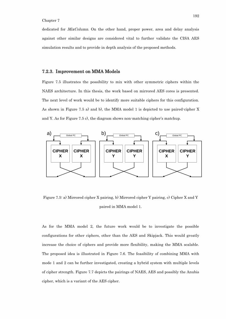
192
Chapter 7
dedicated for MixColumn. On the other hand, proper power, area and delay analysis
against other similar designs are considered vital to further validate the CISA AES
simulation results and to provide in depth analysis of the proposed methods.
7.2.3. Improvement on MMA Models
Figure 7.5 illustrates the possibility to mix with other symmetric ciphers within the
NAES architecture. In this thesis, the work based on mirrored AES cores is presented.
The next level of work would be to identify more suitable ciphers for this configuration.
As shown in Figure 7.5 a) and b), the MMA model 1 is depicted to use paired-cipher X
and Y. As for Figure 7.5 c), the diagram shows non-matching cipher’s matchup.
CIPHER
X
CIPHER
X
Global PC
CIPHER
Y
CIPHER
Y
Global PC
CIPHER
X
CIPHER
Y
Global PCa) b) c)
Figure 7.5: a) Mirrored cipher X pairing, b) Mirrored cipher Y pairing, c) Cipher X and Y
paired in MMA model 1.
As for the MMA model 2, the future work would be to investigate the possible
configurations for other ciphers, other than the AES and Skipjack. This would greatly
increase the choice of ciphers and provide more flexibility, making the MMA scalable.
The proposed idea is illustrated in Figure 7.6. The feasibility of combining MMA with
mode 1 and 2 can be further investigated, creating a hybrid system with multiple levels
of cipher strength. Figure 7.7 depicts the pairings of NAES, AES and possibly the Anubis
cipher, which is a variant of the AES cipher.
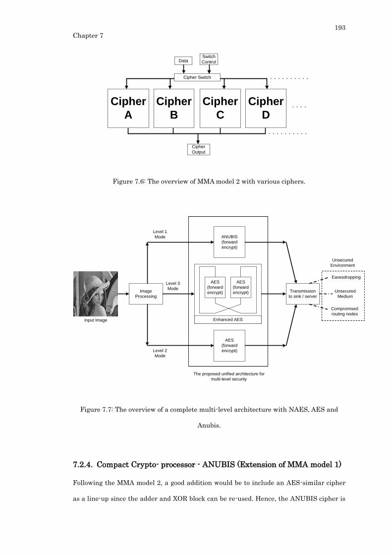
193
Chapter 7
Cipher
A
Cipher
B
Cipher Switch
Cipher
Output
DataSwitch
Control
Cipher
C
Cipher
D
Figure 7.6: The overview of MMA model 2 with various ciphers.
Image
Processing
ANUBIS
(forward
encrypt)
AES
(forward
encrypt)
Enhanced AES
AES
(forward
encrypt)
AES
(forward
encrypt)
Input Image
Level 1
Mode
Level 2
Mode
Level 3
ModeTransmission
to sink / server
Unsecured
Medium
Compromised
routing nodes
Eavesdropping
The proposed unified architecture for
multi-level security
Unsecured
Environment
Figure 7.7: The overview of a complete multi-level architecture with NAES, AES and
Anubis.
7.2.4. Compact Crypto- processor - ANUBIS (Extension of MMA model 1)
Following the MMA model 2, a good addition would be to include an AES-similar cipher
as a line-up since the adder and XOR block can be re-used. Hence, the ANUBIS cipher is
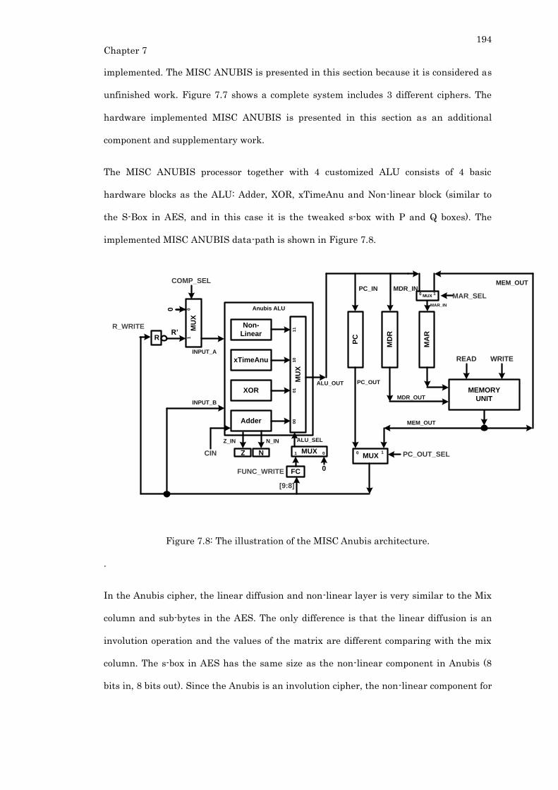
194
Chapter 7
implemented. The MISC ANUBIS is presented in this section because it is considered as
unfinished work. Figure 7.7 shows a complete system includes 3 different ciphers. The
hardware implemented MISC ANUBIS is presented in this section as an additional
component and supplementary work.
The MISC ANUBIS processor together with 4 customized ALU consists of 4 basic
hardware blocks as the ALU: Adder, XOR, xTimeAnu and Non-linear block (similar to
the S-Box in AES, and in this case it is the tweaked s-box with P and Q boxes). The
implemented MISC ANUBIS data-path is shown in Figure 7.8.
MD
R
MA
R
MAR_SEL
[9:8]
FUNC_WRITE
MU
X1
0
RR’
0
MEMORY
UNIT
READ WRITE
N
CIN
FC
Anubis ALU
Adder
XOR
xTimeAnu
Non-
Linear
Z_IN
Z
N_IN
MU
X0
00
11
01
1
MUX1 0
PC_IN MDR_IN
MAR_IN
COMP_SEL
PC
0
MUX0 1
MUX0 1 PC_OUT_SEL
PC_OUT
MEM_OUT
MDR_OUTINPUT_B
INPUT_A
R_WRITE
MEM_OUT
ALU_OUT
ALU_SEL
Figure 7.8: The illustration of the MISC Anubis architecture.
.
In the Anubis cipher, the linear diffusion and non-linear layer is very similar to the Mix
column and sub-bytes in the AES. The only difference is that the linear diffusion is an
involution operation and the values of the matrix are different comparing with the mix
column. The s-box in AES has the same size as the non-linear component in Anubis (8
bits in, 8 bits out). Since the Anubis is an involution cipher, the non-linear component for
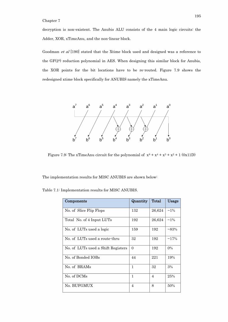
195
Chapter 7
decryption is non-existent. The Anubis ALU consists of the 4 main logic circuits: the
Adder, XOR, xTimeAnu, and the non-linear block.
Goodman et al [190] stated that the Xtime block used and designed was a reference to
the GF(28) reduction polynomial in AES. When designing this similar block for Anubis,
the XOR points for the bit locations have to be re-routed. Figure 7.9 shows the
redesigned xtime block specifically for ANUBIS namely the xTimeAnu.
b7
b6
b5
b4
b3
b2
b1
b0
a7
a6
a5
a4
a3
a2
a1
a0
Figure 7.9: The xTimeAnu circuit for the polynomial of x8 + x4 + x3 + x2 + 1 (0x11D)
The implementation results for MISC ANUBIS are shown below:
Table 7.1: Implementation results for MISC ANUBIS.
Components Quantity Total Usage
No. of Slice Flip Flops 132 26,624 ~1%
Total No. of 4 Input LUTs 192 26,624 ~1%
No. of LUTs used a logic 159 192 ~83%
No. of LUTs used a route-thru 32 192 ~17%
No. of LUTs used a Shift Registers 0 192 0%
No. of Bonded IOBs 44 221 19%
No. of BRAMs 1 32 3%
No. of DCMs 1 4 25%
No. BUFGMUX 4 8 50%
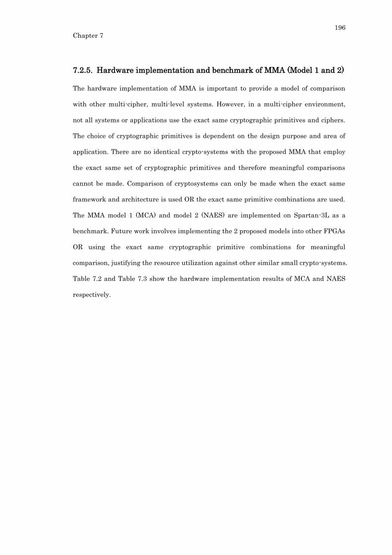
196
Chapter 7
7.2.5. Hardware implementation and benchmark of MMA (Model 1 and 2)
The hardware implementation of MMA is important to provide a model of comparison
with other multi-cipher, multi-level systems. However, in a multi-cipher environment,
not all systems or applications use the exact same cryptographic primitives and ciphers.
The choice of cryptographic primitives is dependent on the design purpose and area of
application. There are no identical crypto-systems with the proposed MMA that employ
the exact same set of cryptographic primitives and therefore meaningful comparisons
cannot be made. Comparison of cryptosystems can only be made when the exact same
framework and architecture is used OR the exact same primitive combinations are used.
The MMA model 1 (MCA) and model 2 (NAES) are implemented on Spartan-3L as a
benchmark. Future work involves implementing the 2 proposed models into other FPGAs
OR using the exact same cryptographic primitive combinations for meaningful
comparison, justifying the resource utilization against other similar small crypto-systems.
Table 7.2 and Table 7.3 show the hardware implementation results of MCA and NAES
respectively.

197
Chapter 7
Table 7.2: Implementation results for multi-cipher architecture MMA mode 1 (MCA -
AES and Skipjack coupling) on Spartan-3L.
Components Quantity Total Usage
No. of Slice Flip Flops 196 26,624 ~1%
No. of Occupied Slices 315 13,312 2%
Total No. of 4 Input LUTs 588 26,624 2%
No. of LUTs used a logic 519 588 88%
No. of LUTs used a route-thru 68 588 12%
No. of LUTs used a Shift Registers 1 588 ~0%
No. of Bonded IOBs 44 221 19%
No. of BRAMs 3 32 9%
No. of GCLKs 4 8 50%
No. of DCMs 1 4 25%
Table 7.3: Implementation results for multi-cipher architecture MMA mode 2 (NAES -
AES and AES coupling) on Spartan-3L.
Components Quantity Total Usage
No. of Slice Flip Flops 706 26,624 2.65%
No. of Occupied Slices 1117 13,312 8%
Total No. of 4 Input LUTs 1270 26,624 4%
No. of LUTs used a logic 1161 1270 ~91%
No. of LUTs used a route-thru 106 1270 9%
No. of LUTs used a Shift Registers 3 1270 ~0%
No. of Bonded IOBs 36 221 16%
No. of BRAMs 6 32 18%
No. of GCLKs 4 8 50%
No. of DCMs 1 4 25%
198
Chapter 7
7.2.6. The Proper Hardware Validation and Verification of the Proposed
SEA
The final objective of the research development presented in this thesis is the
implementation of selective encryption architecture (SEA). The objective is achieved
through the combination a MIPS SPIHT visual processor and the proposed CISA AES.
The proposed SEA is intended to demonstrate real-world practicality by employing one of
the proposed architecture and an image processor to form a joint encryption system. The
hardware implementation of SEA and the implementation results are presented in
Chapter 6. The whole system is able to demonstrate a four-frame image capture, on-
board image processing and compression, encryption, and transmission to a local
connected computer. The transmitted data is then received, decrypted, decompressed on
the connected computer and displayed onto a display monitor.
Despite having the main objective achieved by designing low-area, low-complexity
crypto-processors, the final product of the joint encryption system is yet to be
benchmarked. The SEA is difficult to be benchmarked with other works mainly because
there are no known other works to compare the design with as a whole. To achieve fair
comparison, the point of comparison has to be a single system with both a crypto-
processor and an image processor. The SEA can be a benchmark of its own by setting an
example of any other SEA related future works and thus, the proposed SEA also has to
be properly validated through behavioural and post-route simulations in the future.
199
REFERENCE
[1] M. A. Khan, M. Sharma, and B. P. R, "A Survey of RFID Tags " International
Journal of Recent Trends in Engineering, vol. 1, p. 4, 2009.
[2] A. S. A. Mason, A.I. Al-Shamma, T. Welsby, "RFID and Wireless Sensor Network
Integration for Intelligent Asset Tracking Systems," in 2nd GERI Annual
Research Symposium GARS-2006, June 15 2006 ed. Liverpool, UK, 2006.
[3] M. Buettner, B. Greenstein, A. Sample, J. R. Smith, and D. Wetheral, "Revisiting
Smart Dust with RFID Sensor Networks," in Proc. 7th ACM Workshop on Hot
Topics in Networks (Hotnets-VII), 2008.
[4] M. Buettner, R. Prasad, A. Sample, D. Yeager, B. Greenstein, J. R. Smith, and D.
Wetherall, "RFID sensor networks with the Intel WISP," presented at the
Proceedings of the 6th ACM conference on Embedded network sensor systems,
Raleigh, NC, USA, 2008.
[5] Z. Kai and G. Lina, "A Survey on the Internet of Things Security," in
Computational Intelligence and Security (CIS), 2013 9th International
Conference on, 2013, pp. 663-667.
[6] R. Roman, C. Alcaraz, and J. Lopez, "A survey of cryptographic primitives and
implementations for hardware-constrained sensor network nodes," Mob. Netw.
Appl., vol. 12, pp. 231-244, 2007.
[7] J. Smith, A. Sample, P. Powledge, S. Roy, and A. Mamishev, "A Wirelessly-
Powered Platform for Sensing and Computation," in UbiComp 2006: Ubiquitous
Computing. vol. 4206, P. Dourish and A. Friday, Eds., ed: Springer Berlin
Heidelberg, 2006, pp. 495-506.
[8] A. P. Sample, D. J. Yeager, P. S. Powledge, A. V. Mamishev, and J. R. Smith,
"Design of an RFID-Based Battery-Free Programmable Sensing Platform,"
Instrumentation and Measurement, IEEE Transactions on, vol. 57, pp. 2608-
2615, 2008.
200
[9] A. de la Piedra, A. Braeken, and A. Touhafi, "Sensor Systems Based on FPGAs
and Their Applications: A Survey," Sensors, vol. 12, p. 12235, 2012.
[10] A. K. Jones, R. Hoare, S. Dontharaju, S. Tung, R. Sprang, J. Fazekas, J. T. Cain,
and M. H. Mickle, "An automated, FPGA-based reconfigurable, low-power RFID
tag," Microprocess. Microsyst., vol. 31, pp. 116-134, 2007.
[11] L. Ang, K. P. Seng, L. S. Yeong, L. W. Chew, and W. C. Chia, Wireless
Multimedia Sensor Networks on Reconfigurable Hardware: Information
Reduction Techniques: Springer-Verlag New York Incorporated, 2013.
[12] J. Liao, B. Singh, M. Khalid, and K. Tepe, "FPGA based wireless sensor node
with customizable event-driven architecture," EURASIP Journal on Embedded
Systems, vol. 2013, pp. 1-11, 2013/04/19 2013.
[13] B. Tavli, K. Bicakci, R. Zilan, and J. Barcelo-Ordinas, "A survey of visual sensor
network platforms," Multimedia Tools and Applications, vol. 60, pp. 689-726,
2012/10/01 2012.
[14] S. Soro and W. Heinzelman, "A Survey of Visual Sensor Networks," Advances in
Multimedia, vol. 2009, 2009.
[15] C. Mangesh, S. Claudio, P. Matteo, P. Paolo, L. Giuseppe, and S. Luca,
"Distributed Visual Surveillance with Resource Constrained Embedded
Systems," in Visual Information Processing in Wireless Sensor Networks:
Technology, Trends and Applications, A. Li-Minn and S. Kah Phooi, Eds., ed
Hershey, PA, USA: IGI Global, 2012, pp. 272-292.
[16] M. T. Lazarescu, "Design of a WSN platform for long-term environmental
monitoring for IoT applications," Emerging and Selected Topics in Circuits and
Systems, IEEE Journal on, vol. 3, pp. 45-54, 2013.
[17] M. A. M. Vieira, C. N. Coelho Jr, D. da Silva, and J. M. da Mata, "Survey on
wireless sensor network devices," in Emerging Technologies and Factory
Automation, 2003. Proceedings. ETFA'03. IEEE Conference, 2003, pp. 537-544.
[18] D. G. Bailey, Design for embedded image processing on FPGAs: John Wiley &
Sons, 2011.

201
[19] Y. W. Law, J. Doumen, and P. Hartel, "Survey and benchmark of block ciphers
for wireless sensor networks," ACM Trans. Sen. Netw., vol. 2, pp. 65-93, 2006.
[20] Z. Li and G. Gong, "A Survey on Security in Wireless Sensor Networks,"
University of Waterloo, Waterloo, Ontario, Canada, http://cacr.uwaterloo.ca/ 20,
2008.
[21] P. Ganesan, R. Venugopalan, P. Peddabachagari, A. Dean, F. Mueller, and M.
Sichitiu, "Analyzing and modeling encryption overhead for sensor network
nodes," presented at the Proceedings of the 2nd ACM international conference on
Wireless sensor networks and applications, San Diego, CA, USA, 2003.
[22] J. Aragones-vilella, A. Martínez-ballesté, and A. Solanas, "A Brief Survey on
RFID Privacy and Security," presented at the World Congress on Engineering,
2007.
[23] R. Anderson, M. Bond, J. Clulow, and S. Skorobogatov, "Cryptographic
processors-a survey," Proceedings of the IEEE, vol. 94, pp. 357-369, 2006.
[24] M. K. Hani, H. Y. Wen, and A. Paniandi, "Design and implementation of a
private and public key crypto processor for next-generation it security
applications," Malaysian Journal of Computer Science, vol. 19, pp. 29-45, 2006.
[25] J. Sen, "A Survey on Wireless Sensor Network Security," International Journal of
Vommunication Networks and Information Security (IJCNIS), vol. 1, p. 24,
August 2010 2009.
[26] D. Westhoff, J. Girao, and A. Sarma, "Security solutions for wireless sensor
networks," NEC Journal of Advanced Technology, vol. 59, 2006.
[27] R. C. Merkle and M. E. Hellman, "On the security of multiple encryption,"
Communications of the ACM, vol. 24, pp. 465-467, 1981.
[28] J. Kushwaha and B. N. Roy, "Secure image data by double encryption,"
International Journal of Computer Applications (0975–8887), vol. 5, pp. 28-32,
2010.
[29] C.-C. C. Chung-Ping Young, Yen-Bor Lin and Liang-Bi Chen, "Fast Multi-cipher
Transformation and its Implementation for Modern Secure Protocols,"

202
International Journal of Innovative Computing, Information and Control, vol. 7,
pp. 4941- 4954, August 2011 2011.
[30] Y. Chung-Ping, C. Chung-Chu, C. Liang-Bi, and H. Ing-Jer, "NCPA: A
Scheduling Algorithm for Multi-cipher and Multi-mode Reconfigurable
Cryptosystem," in Intelligent Information Hiding and Multimedia Signal
Processing, 2008. IIHMSP '08 International Conference on, 2008, pp. 1356-1359.
[31] F. Bagci, T. Ungerer, and N. Bagherzadeh, "Multi-level Security in Wireless
Sensor Networks," International Journal on Advances in Software Volume 2,
Number 4, 2009, 2009.
[32] D. Schürmann, "Encryption and Key Exchange in Wireless Sensor Networks,"
2013.
[33] R. Yasmin, E. Ritter, and G. Wang, "An authentication framework for wireless
sensor networks using identity-based signatures," in Computer and Information
Technology (CIT), 2010 IEEE 10th International Conference on, 2010, pp. 882-
889.
[34] G. Panić, T. Basmer, S. Henry, S. Peter, F. Vater, and K. Tittelbach-Helmrich,
"Design of a sensor node crypto processor for ieee 802.15. 4 applications," in SOC
Conference (SOCC), 2012 IEEE International, 2012, pp. 213-217.
[35] M. Grand, L. Bossuet, G. Gogniat, B. L. Gal, J.-P. Delahaye, and D. Dallet, "A
Reconfigurable Multi-core Cryptoprocessor for Multi-channel Communication
Systems," presented at the Proceedings of the 2011 IEEE International
Symposium on Parallel and Distributed Processing Workshops and PhD Forum,
2011.
[36] T. Eisenbarth and S. Kumar, "A Survey of Lightweight-Cryptography
Implementations," Design & Test of Computers, IEEE, vol. 24, pp. 522-533, 2007.
[37] T. Winkler and B. Rinner, "Security and Privacy Protection in Visual Sensor
Networks: A Survey," University of Klagenfurt2012.
[38] J. Lee, K. Kapitanova, and S. H. Son, "The price of security in wireless sensor
networks," Comput. Netw., vol. 54, pp. 2967-2978, 2010.

203
[39] Y.-C. Wang, "Data compression techniques in wireless sensor networks,"
Pervasive Computing, New York: Nova Science Publishers, Inc, 2012.
[40] G. S. Quirino, A. R. Ribeiro, and E. D. Moreno, Asymmetric Encryption in
Wireless Sensor Networks: INTECH Open Access Publisher, 2012.
[41] A. Massoudi, F. Lefebvre, C. D. Vleeschouwer, B. Macq, and J.-J. Quisquater,
"Overview on selective encryption of image and video: challenges and
perspectives," EURASIP J. Inf. Secur., vol. 2008, pp. 1-18, 2008.
[42] H. Cheng and L. Xiaobo, "Partial encryption of compressed images and videos,"
Signal Processing, IEEE Transactions on, vol. 48, pp. 2439-2451, 2000.
[43] R. V. Kulkarni, A. Forster, and G. K. Venayagamoorthy, "Computational
Intelligence in Wireless Sensor Networks: A Survey," IEEE Communications
Surveys & Tutorials, vol. 13, pp. 68-96, 2011.
[44] A. Juels, "Minimalist Cryptography for Low-Cost RFID Tags (Extended
Abstract)," in Security in Communication Networks. vol. 3352, C. Blundo and S.
Cimato, Eds., ed: Springer Berlin Heidelberg, 2005, pp. 149-164.
[45] J. Kůr and V. Matyáš, "An Adaptive Security Architecture for Location Privacy
Sensitive Sensor Network Applications," in Lightweight Cryptography for
Security and Privacy, ed: Springer, 2013, pp. 81-96.
[46] A.-S. K. Pathan, H.-W. Lee, and C. S. Hong, "Security in wireless sensor
networks: issues and challenges," in Advanced Communication Technology, 2006.
ICACT 2006. The 8th International Conference, 2006, pp. 6 pp.-1048.
[47] P. Jamieson, W. Luk, S. J. E. Wilton, and G. A. Constantinides, "An energy and
power consumption analysis of FPGA routing architectures," in Field-
Programmable Technology, 2009. FPT 2009. International Conference on, 2009,
pp. 324-327.
[48] J. Lamoureux and W. Luk, "An Overview of Low-Power Techniques for Field-
Programmable Gate Arrays," in Adaptive Hardware and Systems, 2008. AHS '08.
NASA/ESA Conference on, 2008, pp. 338-345.

204
[49] G. Gong, "Lightweight Cryptography for RFID Systems," in International
Conference on Cryptology in India (Tutorial Talk), Hyderabad, India, 2010.
[50] A. K. Lenstra and E. R. Verheul, "Selecting Cryptographic Key Sizes," J. Cryptol.,
vol. 14, pp. 255-293, 2001.
[51] A. K. Lenstra, "Key lengths," Wiley2006.
[52] E. N. I. S. A. (ENISA), "Algorithms, Key Sizes and Parameters Report - 2014
recommendations," ENISA, http://www.enisa.europa.eu2014.
[53] P. A. Laplante, "A novel single instruction computer architecture," SIGARCH
Comput. Archit. News, vol. 18, pp. 22-26, 1990.
[54] W. F. Gilreath and P. A. Laplante, Computer architecture: a minimalist
perspective: Kluwer Academic Publishers, 2003.
[55] W. F. Gilreath and P. A. Laplante, Computer Architecture: Kluwer Academic
Publishers, 2003.
[56] F. M. a. B. Parhami, "URISC: The ultimate reduced instruction set computer,"
Department of Computer Science, University of WaterlooJune 1987 1987.
[57] P. Laplante and W. Gilreath, "One Instruction Set Computers for Image
Processing," J. VLSI Signal Process. Syst., vol. 38, pp. 45-61, 2004.
[58] N. Tsoutsos and M. Maniatakos, "Investigating the Application of One
Instruction Set Computing for Encrypted Data Computation," in Security,
Privacy, and Applied Cryptography Engineering. vol. 8204, B. Gierlichs, S.
Guilley, and D. Mukhopadhyay, Eds., ed: Springer Berlin Heidelberg, 2013, pp.
21-37.
[59] C. Ayantika and S. Indranil, "FURISC: FHE Encrypted URISC Design," IACR
Cryptology ePrint Archive, p. 11, 2015.
[60] N. G. Tsoutsos and M. Maniatakos, "HEROIC: Homomorphically EncRypted One
Instruction Computer," in Design, Automation and Test in Europe Conference
and Exhibition (DATE), 2014, 2014, pp. 1-6.
[61] C. Xiangqian, M. Kia, Y. Kang, and N. Pissinou, "Sensor network security: a
survey," Communications Surveys & Tutorials, IEEE, vol. 11, pp. 52-73, 2009.

205
[62] Z. Xueying, H. M. Heys, and L. Cheng, "Energy efficiency of symmetric key
cryptographic algorithms in wireless sensor networks," in Communications
(QBSC), 2010 25th Biennial Symposium on, 2010, pp. 168-172.
[63] N. National Institute of Standards and Technology, "SKIPJACK and KEA
Algorithm Specifications Version 2.0," National Institute of Standards and
Technology (NIST)Mai 1998.
[64] C. Karlof, N. Sastry, and D. Wagner, "TinySec: a link layer security architecture
for wireless sensor networks," presented at the Proceedings of the 2nd
international conference on Embedded networked sensor systems, Baltimore, MD,
USA, 2004.
[65] J. Daemen and V. Rijmen, "The Block Cipher Rijndael," presented at the
Proceedings of the The International Conference on Smart Card Research and
Applications, 2000.
[66] A. Dandalis, V. K. Prasanna, and J. D. P. Rolim, "A Comparative Study of
Performance of AES Final Candidates Using FPGAs," presented at the
Proceedings of the Second International Workshop on Cryptographic Hardware
and Embedded Systems, 2000.
[67] F. Büsching, A. Figur, D. Schürmann, and L. Wolf, "Utilizing Hardware AES
Encryption for WSNs," in The 10th European Conference on Wireless Sensor
Networks, EWSN 2013, Ghent, Belgium, 2013, pp. 33-36.
[68] A. Satoh, S. Morioka, K. Takano, and S. Munetoh, "A Compact Rijndael
Hardware Architecture with S-Box Optimization," presented at the Proceedings
of the 7th International Conference on the Theory and Application of Cryptology
and Information Security: Advances in Cryptology, 2001.
[69] D. Canright, "A very compact s-box for AES," presented at the Proceedings of the
7th international conference on Cryptographic hardware and embedded systems,
Edinburgh, UK, 2005.
206
[70] P. V. S. Shastry, A. Agnihotri, D. Kachhwaha, J. Singh, and M. S. Sutaone, "A
combinational logic implementation of S-box of AES," in Circuits and Systems
(MWSCAS), 2011 IEEE 54th International Midwest Symposium on, 2011, pp. 1-4.
[71] J. Boyar and R. Peralta, "A Small Depth-16 Circuit for the AES S-Box," in
Information Security and Privacy Research. vol. 376, D. Gritzalis, S. Furnell, and
M. Theoharidou, Eds., ed: Springer Berlin Heidelberg, 2012, pp. 287-298.
[72] D. Canright and L. Batina, "A very compact "Perfectly masked" S-box for AES,"
presented at the Proceedings of the 6th international conference on Applied
cryptography and network security, NewYork, NY, USA, 2008.
[73] Y. Lin and Q. Gang, "Design space exploration for energy-efficient secure sensor
network," in Application-Specific Systems, Architectures and Processors, 2002.
Proceedings. The IEEE International Conference on, 2002, pp. 88-97.
[74] G. Sharma, S. Bala, and A. K. Verma, "Security frameworks for wireless sensor
networks-review," Procedia Technology, vol. 6, pp. 978-987, 2012.
[75] K. Sharma;, M. K. Ghose;, and Kuldeep;, "Complete Security Framework for
Wireless Sensor Networks," (IJCSIS) International Journal of Computer Science
and Information Security, vol. 3, 2009.
[76] C. Lee, L. Yin, and Y. Guo, "A Cluster-Based Multilevel Security Model for
Wireless Sensor Networks," in Intelligent Information Processing VI, ed:
Springer, 2012, pp. 320-330.
[77] Y. Chung-Ping, L. Yen-Bor, and C. Chung-Chu, "Software and hardware design
of a multi-cipher cryptosystem," in TENCON 2009 - 2009 IEEE Region 10
Conference, 2009, pp. 1-5.
[78] L. Wu, C. Weaver, and T. Austin, "CryptoManiac: a fast flexible architecture for
secure communication," SIGARCH Comput. Archit. News, vol. 29, pp. 110-119,
2001.
[79] R. Norcen and A. Uhl, "Selective Encryption of the JPEG2000 Bitstream," in
Communications and Multimedia Security. Advanced Techniques for Network
207
and Data Protection. vol. 2828, A. Lioy and D. Mazzocchi, Eds., ed: Springer
Berlin Heidelberg, 2003, pp. 194-204.
[80] S. Lian, J. Sun, D. Zhang, and Z. Wang, "A Selective Image Encryption Scheme
Based on JPEG2000 Codec," in Advances in Multimedia Information Processing -
PCM 2004. vol. 3332, K. Aizawa, Y. Nakamura, and S. i. Satoh, Eds., ed:
Springer Berlin Heidelberg, 2005, pp. 65-72.
[81] M. Feldhofer, S. Dominikus, and J. Wolkerstorfer, "Strong Authentication for
RFID Systems Using the AES Algorithm," in Cryptographic Hardware and
Embedded Systems - CHES 2004. vol. 3156, M. Joye and J.-J. Quisquater, Eds.,
ed: Springer Berlin / Heidelberg, 2004, pp. 85-140.
[82] A. Juels and S. Weis, "Authenticating Pervasive Devices with Human Protocols,"
in Advances in Cryptology – CRYPTO 2005. vol. 3621, V. Shoup, Ed., ed:
Springer Berlin Heidelberg, 2005, pp. 293-308.
[83] D. W. Carman, P. S. Kruus, and B. J. Matt, "Constraints and approaches for
distributed sensor network security," Cryptographic Technologies Group Trusted
Information Systems, The Security Research Division of Network Associates, Inc.
2000.
[84] D. Kundur, W. Luh, U. N. Okorafor, and T. Zourntos, "Security and Privacy for
Distributed Multimedia Sensor Networks," Proceedings of the IEEE, vol. 96, pp.
112-130, 2008.
[85] B. Furht and D. Kirovski, Multimedia encryption and authentication techniques
and applications: Auerbach Publications, 2006.
[86] S. H. Kamali, R. Shakerian, M. Hedayati, and M. Rahmani, "A new modified
version of Advanced Encryption Standard based algorithm for image encryption,"
in Electronics and Information Engineering (ICEIE), 2010 International
Conference On, 2010, pp. V1-141-V1-145.
[87] M. M. Z. Medien, K. Lazhar, B. Adel, and T. Rached, "A Modified AES Based
Algorithm for Image Encryption," Int. Journal of Computer Science and
Engineering, vol. 1, pp. 70-75, 2007.

208
[88] F. R. Sumira Hameed, Riaz Moghal, Gulraiz Akhtar, Anil Ahmed, Abdul Ghafoor
Dar, "Modified Advanced Encryption Standard For Text And Images "
Conmputer Science Journal, vol. 1, p. 10, 2011.
[89] S. Lian, Multimedia Content Encryption: Techniques and Applications: CRC
Press, 2008.
[90] S. A. El-said, K. F. Hussein, and M. M. Fouad, "Confidentiality and privacy for
videos storage and transmission," The International Journal of Advances in
Science and Technology, vol. 28, pp. 67-88, 2011.
[91] T. Lookabaugh and D. C. Sicker, "Selective encryption for consumer
applications," Communications Magazine, IEEE, vol. 42, pp. 124-129, 2004.
[92] E. N. Mui. (2007). Practical Implementation of Rijndael S-Box Using
Combinational Logic (2007). Available:
http://www.xess.com/projects/Rijndael_SBox.pdf
[93] Z. Xinmiao and K. K. Parhi, "High-speed VLSI architectures for the AES
algorithm," Very Large Scale Integration (VLSI) Systems, IEEE Transactions on,
vol. 12, pp. 957-967, 2004.
[94] T. Cevik, A. Gunagwera, and N. Cevik, "A survey of multimedia streaming in
wireless sensor networks: progress, issues and design challenges," International
Journal of Computer Networks & Communications (IJCNC), vol. 7, 2015.
[95] M. Hempstead, M. J. Lyons, D. Brooks, and G.-Y. Wei, "Survey of Hardware
Systems for Wireless Sensor Networks," Journal of Low Power Electronics, vol. 4,
pp. 11-20, 2008.
[96] A. Juels, "RFID security and privacy: a research survey," Selected Areas in
Communications, IEEE Journal on, vol. 24, pp. 381-394, 2006.
[97] S. E. Sarma, S. A. Weis, and D. W. Engels, "RFID Systems and Security and
Privacy Implications," presented at the Revised Papers from the 4th
International Workshop on Cryptographic Hardware and Embedded Systems,
2003.
209
[98] Z. Lei and W. Zhi, "Integration of RFID into Wireless Sensor Networks:
Architectures, Opportunities and Challenging Problems," in Grid and
Cooperative Computing Workshops, 2006. GCCW '06. Fifth International
Conference on, 2006, pp. 463-469.
[99] M. Sethi, J. Arkko, and A. Keranen, "End-to-end security for sleepy smart object
networks," in Local Computer Networks Workshops (LCN Workshops), 2012
IEEE 37th Conference on, 2012, pp. 964-972.
[100] M. Bhandarkar, Analysis of sLEACH for improvement of network lifetime in
Wireless Sensor Networks: ProQuest, 2008.
[101] H. S. Aghdasi, M. Abbaspour, M. E. Moghadam, and Y. Samei, "An energy-
efficient and high-quality video transmission architecture in wireless video-based
sensor networks," Sensors, vol. 8, pp. 4529-4559, 2008.
[102] M. Guerrero-Zapata, R. Zilan, J. Barceló-Ordinas, K. Bicakci, and B. Tavli, "The
future of security in Wireless Multimedia Sensor Networks," Telecommunication
Systems, vol. 45, pp. 77-91, 2010/09/01 2010.
[103] J. López and J. Zhou, Wireless sensor network security vol. 1: IOS Press, 2008.
[104] M. Johnson, M. Healy, P. van de Ven, M. J. Hayes, J. Nelson, T. Newe, and E.
Lewis, "A comparative review of wireless sensor network mote technologies," in
Sensors, 2009 IEEE, 2009, pp. 1439-1442.
[105] D. C. Ranasinghe, D. Lim, P. H. Cole, and S. Devadas, "A low cost solution to
authentication in passive RFID systems," 2006.
[106] A. Industries, "RFID Selection Guide," in Version 1, ed, 2010.
[107] IBTechnology. (2013, 21 June). List of supported tag types and key features.
Available: http://www.ibtechnology.co.uk/pdf/tag_types.pdf
[108] D. D. Deavours, "UHF EPC Tag Performance Evaluation," University of Kansas,
RFID Alliance Lab2005.
[109] S. Bukkapatnam, J. M. Govardhan, S. Hariharan, V. Rajamani, B. Gardner, and
A. Contreras, "Report of Work Conducted under the AEGIS or CELDi Strategic

210
Research Grant 2005 “Experimental Test Bed for Performance Evaluation of
RFID Systems”," Oklahoma State University, Stillwater OK2005.
[110] I. T. Corporation. (2012, 21 June). Intermec RFID Tags & Media - Meeting the
scalable RFID challenge.
[111] N. Corporation. (2008, 21 June). Item Level Tagging Selector Guide
[112] A. D. Inc. (2013, 21 June). HF RFID Inlays.
[113] A. D. Inc. (2013, 21 June). UHF RFID Inlays. Available:
http://nashua.com/Resources/ProductSheets/10049-EPCSelecGuide.pdf
[114] N. Corporation. (2008). EPC RFID Label Selector Guide. Available:
http://nashua.com/Resources/ProductSheets/10049-EPCSelecGuide.pdf
[115] M. Buettner, B. Greenstein, and D. Wetherall, "Dewdrop: an energy-aware
runtime for computational RFID," in Proc. USENIX NSDI, 2011, pp. 197-210.
[116] B. R. Elbal, "Measurement Based Evaluation of the Wireless Identification and
Sensing Platform," Vienna University of Technology, 2015.
[117] H. Kopetz, "Internet of things," in Real-time systems, ed: Springer, 2011, pp. 307-
323.
[118] T. L. Friedman, The world is flat [updated and expanded]: A brief history of the
twenty-first century: Macmillan, 2006.
[119] S. Poslad, "Smart Mobiles, Cards and Device Networks," Ubiquitous Computing:
Smart Devices, Environments and Interactions, pp. 115-133, 2009.
[120] Y. Zhang, L. T. Yang, and J. Chen, RFID and Sensor Networks: Architectures,
Protocols, Security, and Integrations: CRC Press, Inc., 2009.
[121] S. Xin, S. Shijuan, and X. Qingyu, "The integration of Wireless Sensor Networks
and RFID for pervasive computing," in Computer Sciences and Convergence
Information Technology (ICCIT), 2010 5th International Conference on, 2010, pp.
67-72.
[122] M. B. Hai Liu, Amiya Nayak, Ivan Stojmenovic, "Integration of RFID and
Wireless Sensor Networks," presented at the SenseID 2007 Workshop at ACM
SenSys, Sydney, Australia, 2007.

211
[123] U. K. Vishwakarma and R. Shukla, "WSN and RFID: Differences and
Integration," International Journal of Advanced Research in Electronics and
Communication Engineering, vol. 2, pp. 778-780, 2013.
[124] W. C. Chia, W. H. Ngau, L.-M. Ang, K. P. Seng, L. W. Chew, and L. S. Yeong,
"FPGA Technology for Implementation in Visual Sensor Networks," Visual
Information Processing in Wireless Sensor Networks: Technology, Trends and
Applications: Technology, Trends and Applications, p. 293, 2011.
[125] M. Katagi and S. Moriai, "Lightweight cryptography for the internet of things,"
Sony Corporation, pp. 7-10, 2008.
[126] K. Woo Kwon, L. Hwaseong, K. Yong Ho, and L. Dong Hoon, "Implementation
and Analysis of New Lightweight Cryptographic Algorithm Suitable for Wireless
Sensor Networks," in Information Security and Assurance, 2008. ISA 2008.
International Conference on, 2008, pp. 73-76.
[127] S. Vaudenay, "RFID privacy based on public-key cryptography (invited talk)," in
ICISC 2006. LNCS, ed: Springer, 2006, pp. 1--6.
[128] L. Batina, J. Guajardo, T. Kerins, N. Mentens, P. Tuyls, and I. Verbauwhede,
"Public-Key Cryptography for RFID-Tags," in Pervasive Computing and
Communications Workshops, 2007. PerCom Workshops '07. Fifth Annual IEEE
International Conference on, 2007, pp. 217-222.
[129] G. D. Murphy, E. M. Popovici, and W. P. Marnane, "Area-Efficient Processor for
Public-Key Cryptography in Wireless Sensor Networks," in Sensor Technologies
and Applications, 2008. SENSORCOMM '08. Second International Conference on,
2008, pp. 667-672.
[130] Y. Oren and M. Feldhofer, "A low-resource public-key identification scheme for
RFID tags and sensor nodes," presented at the Proceedings of the second ACM
conference on Wireless network security, Zurich, Switzerland, 2009.
[131] S. V. Kaya, E. Sava, A. Levi, zg, r. Er, and etin, "Public key cryptography based
privacy preserving multi-context RFID infrastructure," Ad Hoc Netw., vol. 7, pp.
136-152, 2009.

212
[132] I. F. T. A. S. Sufyan Salim Mahmood AlDabbagh, "Lightweight Block Ciphers: a
comparative study," Journal of Advanced Computer Science and Technology
Research, vol. 2, p. 7, November 2012 2012.
[133] P. Peris-Lopez, Lightweight Cryptography in Radio Frequency Identification
Systems: VDM Publishing, 2010.
[134] R. S. Reddy, "Key management in wireless sensor networks using a modified
Blom scheme," arXiv preprint arXiv:1103.5712, 2011.
[135] O. Sönmez and I. C. Paar, "Symmetric Key Management: Key Derivation and
Key Wrap," Bochum, Germany, February 2009, 2009.
[136] A. Mitrokotsa and C. Douligeris, "Integrated RFID and sensor networks:
architectures and applications," RFID and sensor networks: Architectures,
protocols, security and integrations, pp. 511-535, 2009.
[137] H. Lee, Y. H. Kim, D. H. Lee, and J. Lim, "Classification of key management
schemes for wireless sensor networks," in Advances in Web and Network
Technologies, and Information Management, ed: Springer, 2007, pp. 664-673.
[138] B. Lai, S. Kim, and I. Verbauwhede, "Scalable session key construction protocol
for wireless sensor networks," in IEEE Workshop on Large Scale RealTime and
Embedded Systems (LARTES), 2002, p. 7.
[139] A. Parakh and S. Kak, "Efficient key management in sensor networks," in
GLOBECOM Workshops (GC Wkshps), 2010 IEEE, 2010, pp. 1539-1544.
[140] D. d. O. Gonçalves and D. G. Costa, "A Survey of Image Security in Wireless
Sensor Networks," Journal of Imaging, vol. 1, pp. 4-30, 2015.
[141] P. Peris-Lopez, J. C. Hernandez-Castro, J. M. Tapiador, and A. Ribagorda,
"Advances in Ultralightweight Cryptography for Low-Cost RFID Tags: Gossamer
Protocol," in Information Security Applications, C. Kyo-Il, S. Kiwook, and Y. Moti,
Eds., ed: Springer-Verlag, 2009, pp. 56-68.
[142] M. Y. Malik, "An outline of security in wireless sensor networks: threats,
countermeasures and implementations," arXiv preprint arXiv:1301.3022, 2013.
213
[143] C. Chatmon, T. van Le, and M. Burmester, "Secure anonymous RFID
authentication protocols," Florida State University, Department of Computer
Science, Tech. Rep, 2006.
[144] A. Perrig, J. Stankovic, and D. Wagner, "Security in wireless sensor networks,"
Communications of the ACM, vol. 47, pp. 53-57, 2004.
[145] M. B. I. Reaz, F. Mohd-Yasin, S. L. Tan, H. Y. Tan, and M. I. Ibrahimy, "Partial
encryption of compressed images employing FPGA," in Circuits and Systems,
2005. ISCAS 2005. IEEE International Symposium on, 2005, pp. 2385-2388 Vol.
3.
[146] B. Subramanyan, V. M. Chhabria, and T. G. S. Babu, "Image Encryption Based
on AES Key Expansion," in Emerging Applications of Information Technology
(EAIT), 2011 Second International Conference on, 2011, pp. 217-220.
[147] F. Liu and H. Koenig, "A survey of video encryption algorithms," Computers &
Security, vol. 29, pp. 3-15, 2010.
[148] B. S. PATIL, "Image Security in Wireless Sensor Networks using Quadtree
Coding," in NCRIET-2015 & Indian J.Sci.Res. , 2015, pp. 443 - 447.
[149] J. Molina, C. Leon, J. M. Mora-merchan, and J. Barbancho, Multimedia data
processing and delivery in wireless sensor networks: INTECH Open Access
Publisher, 2010.
[150] M. O. Kulekci, "A Method to Ensure the Confidentiality of the Compressed Data,"
Data Compression, Communications and Processing, International Conference on,
vol. 0, pp. 203-209, 2011.
[151] T. W. Fry and S. A. Hauck, "SPIHT image compression on FPGAs," Circuits and
Systems for Video Technology, IEEE Transactions on, vol. 15, pp. 1138-1147,
2005.
[152] T. Xiang, C. Yu, and F. Chen, "Fast encryption of JPEG 2000 images in wireless
multimedia sensor networks," in Wireless Algorithms, Systems, and Applications,
ed: Springer, 2013, pp. 196-205.
214
[153] A. C. Wu, "Power Efficiency with Data Compression in Wireless Sensor
Networks," ed.
[154] P. H. Cole and D. C. Ranasinghe, Networked RFID systems and lightweight
cryptography: raising barriers to product counterfeiting: Springer, 2008.
[155] A. Poschmann, G. Leander, K. Schramm, and C. Paar, "New Light-Weight Crypto
Algorithms for RFID," in Circuits and Systems, 2007. ISCAS 2007. IEEE
International Symposium on, 2007, pp. 1843-1846.
[156] C. Rolfes, A. Poschmann, G. Leander, and C. Paar, "Ultra-Lightweight
Implementations for Smart Devices --- Security for 1000 Gate Equivalents,"
presented at the Proceedings of the 8th IFIP WG 8.8/11.2 international
conference on Smart Card Research and Advanced Applications, London, UK,
2008.
[157] J. Nechvatal, E. Barker, L. Bassham, W. Burr, and M. Dworkin, "Report on the
development of the Advanced Encryption Standard (AES)," DTIC Document2000.
[158] W. Yong, G. Attebury, and B. Ramamurthy, "A survey of security issues in
wireless sensor networks," Communications Surveys & Tutorials, IEEE, vol. 8,
pp. 2-23, 2006.
[159] I. F. Akyildiz, T. Melodia, and K. R. Chowdhury, "A survey on wireless
multimedia sensor networks," Comput. Netw., vol. 51, pp. 921-960, 2007.
[160] K. Rao, Z. Bojkovic, and D. Milovanovic, Introduction to multimedia
communications: applications, middleware, networking: John Wiley & Sons, 2006.
[161] H. ZainEldin, M. A. Elhosseini, and H. A. Ali, "Image compression algorithms in
wireless multimedia sensor networks: A survey," Ain Shams Engineering Journal,
vol. 6, pp. 481-490, 2015.
[162] L. W. Chew, L.-M. Ang, and K. P. Seng, "Survey of image compression algorithms
in wireless sensor networks," in Information Technology, 2008. ITSim 2008.
International Symposium on, 2008, pp. 1-9.

215
[163] A. Said and W. A. Pearlman, "A new, fast, and efficient image codec based on set
partitioning in hierarchical trees," IEEE Trans. Cir. and Sys. for Video Technol.,
vol. 6, pp. 243-250, 1996.
[164] J. Ritter, G. Fey, and P. Molitor, "SPIHT implemented in a XC4000 device," in
Circuits and Systems, 2002. MWSCAS-2002. The 2002 45th Midwest Symposium
on, 2002, pp. I-239-42 vol.1.
[165] J. Jyotheswar and S. Mahapatra, "Efficient FPGA implementation of DWT and
modified SPIHT for lossless image compression," J. Syst. Archit., vol. 53, pp. 369-
378, 2007.
[166] J. Singh, A. Antoniou, and D. J. Shpak, "Hardware implementation of a wavelet
based image compression coder," in Advances in Digital Filtering and Signal
Processing, 1998 IEEE Symposium on, 1998, pp. 169-173.
[167] M. V. V and M. Mathews, "FPGA Implementation of Image Compression Using
SPIHT Algorithm," International Journal of Advanced Research in Electrical,
Electronics and Instrumentation Engineering, vol. 3, p. 7, January 2014 2014.
[168] P.-Y. Lin, "Basic image compression algorithm and introduction to jpeg
standard," National Taiwan University, Taipei, Taiwan, ROC, 2009.
[169] S. A. Hassan and M. Hussain, "Spatial domain lossless image data compression
method," in Information and Communication Technologies (ICICT), 2011
International Conference on, 2011, pp. 1-4.
[170] H. Wei, Y. Kaidi, Z. Suiyu, J. Han, and X. Zeng, "Unified low cost crypto
architecture accelerating RSA/SHA-1 for security processor," in ASIC, 2009.
ASICON '09. IEEE 8th International Conference on, 2009, pp. 151-154.
[171] L. Jongdeog, S. H. Son, and M. Singhal, "Design of an architecture for multiple
security levels in wireless sensor networks," in Networked Sensing Systems
(INSS), 2010 Seventh International Conference on, 2010, pp. 107-114.
[172] S. R. Afzal, C. Huygens, and W. Joosen, "DiFiSec: An Adaptable Multi-level
Security Framework for Event-Driven Communication in Wireless Sensor

216
Networks," in Network Computing and Applications (NCA), 2012 11th IEEE
International Symposium on, 2012, pp. 263-271.
[173] C. Lee, L.-H. Yin, and Y.-C. Guo, "Poster: A Multilevel Security Model for
Wireless Sensor Networks," ed: IEEE, 2012.
[174] N. Sklavos, A. Priftis, P. Kitsos, and O. Koufopavlou, "Reconfigurable crypto
processor design of encryption algorithms operation modes methods and FPGA
integration," in Circuits and Systems, 2003 IEEE 46th Midwest Symposium on,
2003, pp. 811-814 Vol. 2.
[175] K. HoWon and L. Sunggu, "Design and implementation of a private and public
key crypto processor and its application to a security system," IEEE Transactions
on Consumer Electronics, vol. 50, pp. 214-224, February 2004 2004.
[176] L. Deguang, C. Jinyi, G. Xingdou, Z. Ankang, and L. Conglan, "Parallel AES
algorithm for fast Data Encryption on GPU," in Computer Engineering and
Technology (ICCET), 2010 2nd International Conference on, 2010, pp. V6-1-V6-6.
[177] G. F. Elkabbany, H. K. Aslan, and M. N. Rasslan, "A Design of a Fast Parallel-
Pipelined Implementation of AES: Advanced Encryption Standard," arXiv
preprint arXiv:1501.01427, 2015.
[178] A. Selvi and B. Arunkumar, "Security Enforcement with Cost Assessment for
Cloud Data," International Journal of Innovative Research in Computer and
Communication Engineering, vol. 3, p. 4, February 2015 2015.
[179] F. Y. Y. B.-M. Goi, "FPGA Implementation of Duo - Key Dependent AES,"
International Journal of Cryptology Research, vol. 2, pp. 101 - 109, 2010.
[180] S. Drimer. (2008, March, 2012). Volatile FPGA design security - a survey. 51.
Available: http://www.cl.cam.ac.uk/~sd410/papers/fpga_security.pdf
[181] H. Hinkelmann, A. Reinhardt, S. Varyani, and M. Glesner, "A Reconfigurable
Prototyping Platform for Smart Sensor Networks," in Programmable Logic, 2008
4th Southern Conference on, 2008, pp. 125-130.
[182] S. Misra and E. Eronu, "Implementing Reconfigurable Wireless Sensor Networks:
The Embedded Operating System Approach," Intech, 2012.

217
[183] L. Xu, L. Sun, and X. Zhang, "A UHF RFID Reader Design Based on FPGA," in
Advances in Future Computer and Control Systems, ed: Springer, 2012, pp. 451-
456.
[184] M. Todd, W. Burleson, and R. Tessier, "The design and assessment of a secure
passive RFID sensor system," in New Circuits and Systems Conference
(NEWCAS), 2011 IEEE 9th International, 2011, pp. 494-497.
[185] C. Johnston, K. Gribbon, and D. Bailey, "Implementing image processing
algorithms on FPGAs," in Proceedings of the Eleventh Electronics New Zealand
Conference, ENZCon’04, 2004, pp. 118-123.
[186] B. A. Draper, J. R. Beveridge, A. W. Bohm, C. Ross, and M. Chawathe,
"Accelerated image processing on FPGAs," Image Processing, IEEE Transactions
on, vol. 12, pp. 1543-1551, 2003.
[187] A. E. Nelson, "Implementation of image processing algorithms on FPGA
hardware," Citeseer, 2000.
[188] P. Abhijith, M. Goswami, S. Tadi, and K. Pandey, "Optimized Architecture for
AES," IACR Cryptology ePrint Archive, vol. 2014, p. 540, 2014.
[189] K. Gaj, "Very compact FPGA implementation of the AES algorithm," in
Proceedings of 5th International Workshop on Cryptographic Hardware and
Embedded Systems (CHES), number 2779 in Lecture Notes in Computer Science,
ed: Springer-Verlag, 2003, pp. 319-333.
[190] T. Good and M. Benaissa, "Very small FPGA application-specific instruction
processor for AES," Circuits and Systems I: Regular Papers, IEEE Transactions
on, vol. 53, pp. 1477-1486, 2006.
[191] G. Rouvroy, F. X. Standaert, J. J. Quisquater, and J. D. Legat, "Compact and
efficient encryption/decryption module for FPGA implementation of the AES
Rijndael very well suited for small embedded applications," in Information
Technology: Coding and Computing, 2004. Proceedings. ITCC 2004. International
Conference on, 2004, pp. 583-587 Vol.2.
218
[192] M. Feldhofer, J. Wolkerstorfer, and V. Rijmen, "AES implementation on a grain
of sand," Information Security, IEE Proceedings, vol. 152, pp. 13-20, 2005.
[193] N. Pramstaller and J. Wolkerstorfer, "A universal and efficient AES co-processor
for field programmable logic arrays," in Field Programmable Logic and
Application, ed: Springer, 2004, pp. 565-574.
[194] B. Porter, U. Roedig, and G. Coulson, "Type-safe updating for modular WSN
software," in Distributed Computing in Sensor Systems and Workshops (DCOSS),
2011 International Conference on, 2011, pp. 1-8.
[195] H. Soroush, M. Salajegheh, and T. Dimitriou, "Providing transparent security
services to sensor networks," in Communications, 2007. ICC'07. IEEE
International Conference on, 2007, pp. 3431-3436.
[196] F. Mavadatt and B. Parhami, "URISC: the ultimate reduced instruction set
computer," Int. J. Elect. Enging. Educ., vol. 25, pp. 327-334, 1988.
[197] D. Bhandarkar and D. W. Clark, "Performance from architecture: comparing a
RISC and a CISC with similar hardware organization," in ACM SIGARCH
Computer Architecture News, 1991, pp. 310-319.
[198] C. Chen, G. Novick, and K. Shimano. (2000). RISC architectures. Available:
http://cs.stanford.edu/people/eroberts/courses/soco/projects/risc/about/index.html
[199] O. Mazonka and A. Kolodin, "A simple multi-processor computer based on
subleq," arXiv preprint arXiv:1106.2593, 2011.
[200] F. Mavaddat and B. Parhami, URISC: The Ultimate Reduced Instruction Set
Computer: Fac. of Mathematics, Univ., 1987.
[201] H. Xingze, P. Man-On, and C. C. J. Kuo, "Secure and efficient cryptosystem for
smart grid using homomorphic encryption," in Innovative Smart Grid
Technologies (ISGT), 2012 IEEE PES, 2012, pp. 1-8.
[202] C. Gentry and S. U. C. S. Dept, A fully homomorphic encryption scheme:
Stanford University, 2009.
[203] C. Ting and C. H. Moore, "Mup21 a high performance misc processor," Forth
Dimensions also available at http: www. dnai. com-~ jfox mup21. html, 1995.
219
[204] W. McLoone and J. V. McCanny, "Rijndael FPGA implementation utilizing look-
up tables," in Signal Processing Systems, 2001 IEEE Workshop on, 2001, pp. 349-
360.
[205] V. Fischer and M. Drutarovsk, "Two Methods of Rijndael Implementation in
Reconfigurable Hardware," presented at the Proceedings of the Third
International Workshop on Cryptographic Hardware and Embedded Systems,
2001.
[206] S. Morioka and A. Satoh, "A 10 Gbps full-AES crypto design with a twisted-BDD
S-Box architecture," in Computer Design: VLSI in Computers and Processors,
2002. Proceedings. 2002 IEEE International Conference on, 2002, pp. 98-103.
[207] S. Morioka and A. Satoh, "An Optimized S-Box Circuit Architecture for Low
Power AES Design," in Cryptographic Hardware and Embedded Systems - CHES
2002. vol. 2523, B. Kaliski, ç. Koç, and C. Paar, Eds., ed: Springer Berlin
Heidelberg, 2003, pp. 172-186.
[208] J. Wolkerstorfer, E. Oswald, and M. Lamberger, "An ASIC implementation of the
AES SBoxes," in Topics in Cryptology—CT-RSA 2002, ed: Springer, 2002, pp. 67-
78.
[209] V. Rijmen, "Efficient Implementation of the Rijndael S-box," Katholieke
Universiteit Leuven, Dept. ESAT. Belgium, 2000.
[210] J. Daemen and V. Rijmen, The Design of Rijndael: Springer-Verlag New York,
Inc., 2002.
[211] C. Paar, "Some remarks on efficient inversion in finite fields," in Information
Theory, 1995. Proceedings., 1995 IEEE International Symposium on, 1995, p. 58.
[212] J. Boyar and R. Peralta, "A New Combinational Logic Minimization Technique
with Applications to Cryptology," in Experimental Algorithms. vol. 6049, P. Festa,
Ed., ed: Springer Berlin / Heidelberg, 2010, pp. 178-189.
[213] T. Itoh and S. Tsujii, "A fast algorithm for computing multiplicative inverses in
GF(2m) using normal bases," Inf. Comput., vol. 78, pp. 171-177, 1988.
220
[214] N. Mentens, L. Batina, B. Preneel, and I. Verbauwhede, "A systematic evaluation
of compact hardware implementations for the rijndael s-box," presented at the
Proceedings of the 2005 international conference on Topics in Cryptology, San
Francisco, CA, 2005.
[215] R. Liu and K. K. Parhi, "Fast composite field S-box architectures for advanced
encryption standard," presented at the Proceedings of the 18th ACM Great Lakes
symposium on VLSI, Orlando, Florida, USA, 2008.
[216] S. Piramuthu, "Passive Enumeration of Secret Information in LMAP and M 2 AP
RFID Authentication Protocols," Journal of Information Privacy and Security, vol.
8, pp. 4-14, 2012.
[217] J.-W. Han, C.-S. Park, D.-H. Ryu, and E.-S. Kim, "Optical image encryption
based on XOR operations," Optical Engineering, vol. 38, pp. 47-54, 1999.
[218] Xilinx, "Spartan-3L Low Power FPGA Family," April 18, 2008 2008.
[219] E. Eryilmaz, I. Erturk, and S. Atmaca, "Implementation of Skipjack cryptology
algorithm for WSNs using FPGA," in Application of Information and
Communication Technologies, 2009. AICT 2009. International Conference on,
2009, pp. 1-5.
[220] M. Huang, T. El-Ghazawi, B. Larson, and K. Gaj, "Development of block-cipher
library for reconfigurable computers," in Programmable Logic, 2007. SPL'07.
2007 3rd Southern Conference on, 2007, pp. 191-194.
[221] D. J. Bernstein. (2009). Optimizing linear maps modulo 2. Available:
http://binary.cr.yp.to/linearmod2-20091005.pdf
[222] D. J. Bernstein. (2009, 24-12-2015). sort1.cpp (Optimizing Linear Maps Modulo
2). Available: http://binary.cr.yp.to/linearmod2/sort1.cpp
[223] N. E. Abraham and T. Thomas, "FPGA Implementation of Mix and Inverse Mix
Column for AES Algorithm," International Journal for Scientific Research &
Development (IJSRD), vol. 1, p. 4, 2013.
[224] N. National Institute of Standards and Technology, "Advanced Encryption
Standard," in NIST FIPS PUB 197 U. S. D. o. Commerce, Ed., ed, 2001.
221
[225] T. Good and M. Benaissa, "AES on FPGA from the Fastest to the Smallest," in
Cryptographic Hardware and Embedded Systems – CHES 2005. vol. 3659, J. Rao
and B. Sunar, Eds., ed: Springer Berlin Heidelberg, 2005, pp. 427-440.
[226] H. Feistel and IBM, "Block Cipher Cryptographic System," 1971.
[227] J. Katz and Y. Lindell, Introduction to modern cryptography: CRC Press, 2014.
[228] A. J. Menezes, P. C. V. Oorschot, and S. A. Vanstone, Handbook of applied
cryptography: CRC Press, 1997.
[229] C. Cid and S. Murphy, Algebraic Aspects of the Advanced Encryption Standard.
Springer: Springer Publishing Company, Incorporated, 2006.
[230] A. G. D. Uchoa, M. E. Pellenz, A. O. Santin, and C. A. Maziero, "A Three-Pass
Protocol for Cryptography Based on Padding for Wireless Networks," in 2007 4th
IEEE Consumer Communications and Networking Conference, 2007, pp. 287-291.
[231] Y. Kanamori and S.-M. Yoo, "Quantum three-pass protocol: key distribution
using quantum superposition states," arXiv preprint arXiv:1004.0599, 2010.
[232] A. Jolfaei and A. Mirghadri, "Image Encryption Using Chaos and Block Cipher,"
Computer and Information Science, vol. 4, pp. 172 - 185, January 2011 2011.
[233] J. J. Buchholz. (2001, August 2013). Matlab Implementation of the Advanced
Encryption Standard. Available: http://buchholz.hs-bremen.de/aes/AES.pdf
[234] O. D. Tools. (2016). AES – Symmetric Ciphers Online. Available: http://online-
domain-tools.com/information/about-project
[235] D. P. Menezes and C. M. Dc. Adding Security to Block-Sorting Compression.
[236] H. Li, F. Gao, Y. Xue, and S. Feng, "The Application of LZSS in the RFID Tags,"
in Computer Network and Multimedia Technology, 2009. CNMT 2009.
International Symposium on, 2009, pp. 1-4.
[237] S. Kankonsae, P.Choeysuwan, and S.Choomchuay, "A 2-Stage Compression for
RFID Tags Data," presented at the International Workshop on Information
Communication Technology, KMITL, Bangkok, Thailand, 2010.

222
[238] R. A. Lippert, C. M. Mobarry, and B. P. Walenz, "A space-efficient construction of
the Burrows-Wheeler transform for genomic data," Journal of Computational
Biology, vol. 12, pp. 943-951, 2005.
[239] J. Martinez, R. Cumplido, and C. Feregrino, "An FPGA Parallel Sorting
Architecture for the Burrows Wheeler Transform," presented at the Proceedings
of the 2005 International Conference on Reconfigurable Computing and FPGAs
(ReConFig'05) on Reconfigurable Computing and FPGAs, 2005.
[240] V. Fischer, M. Drutarovsky, P. Chodowiec, and F. Gramain, "InvMixColumn
decomposition and multilevel resource sharing in AES implementations," Very
Large Scale Integration (VLSI) Systems, IEEE Transactions on, vol. 13, pp. 989-
992, 2005.
[241] C. Chitu and M. Glesner, "An FPGA implementation of the AES-Rijndael in
OCB/ECB modes of operation," Microelectronics Journal, vol. 36, pp. 139-146,
2005.

223
APPENDIX I: CELOXICA
HANDLE-C CODES
CISA AES
// AES processor (12bit arch) part ENC
5
#define RC10_TARGET_CLOCK_RATE
20000000
//#define RC10_TARGET_CLOCK_RATE
25175000
//#define PAL_TARGET_CLOCK_RATE 10
20000000
#define ENCRYPT 1
#define DECRYPT 0
15
#include "stdlib.hch"
//#include "pal_master.hch"
//#include "pal_console.hch"
#include "rc10.hch"
20
#define RegWidth 8 // 8 bit long
#define RegWidth_10b 10 //
10 bit long
#define RegWidth_12b 12 //
11 bit long 25
macro expr ClockRate =
RC10_ACTUAL_CLOCK_RATE;
//macro expr ClockRate = 30
PAL_ACTUAL_CLOCK_RATE;
static ram unsigned RegWidth_12b Memory[4096] 35
= {
//example of XOR instruction
//0x301, 0x112, 0x000, // 99 xor 11 = 88
40
//example of SBN instruction
//0x101, 0x112, 0x000, // 99 + 11 = AA
//---------------AES ENCRYPTION / DECRYPTION 45
PROGRAM-----------------//
//PC starts at xxx
0x000, 0x001, 0x002, 0x003, 0x004, 0x005, 0x006,
0x007, 0x008, 0x009, 0x00A, 0x00B, 0x00C, 50
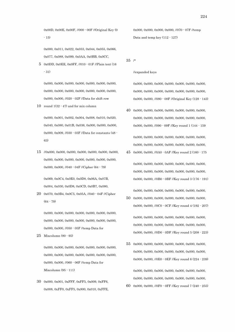
224
0x00D, 0x00E, 0x00F, //000 - 00F //Original Key (0
- 15)
0x000, 0x011, 0x022, 0x033, 0x044, 0x055, 0x066,
0x077, 0x088, 0x099, 0x0AA, 0x0BB, 0x0CC,
0x0DD, 0x0EE, 0x0FF, //010 - 01F //Plain text (16 5
- 31)
0x000, 0x000, 0x000, 0x000, 0x000, 0x000, 0x000,
0x000, 0x000, 0x000, 0x000, 0x000, 0x000, 0x000,
0x000, 0x000, //020 - 02F //Data for shift row
round 1(32 - 47) and for mix column 10
0x000, 0x001, 0x002, 0x004, 0x008, 0x010, 0x020,
0x040, 0x080, 0x01B, 0x036, 0x000, 0x000, 0x000,
0x000, 0x009, //030 - 03F //Data for constants (48 -
63)
//0x000, 0x000, 0x000, 0x000, 0x000, 0x000, 0x000, 15
0x000, 0x000, 0x000, 0x000, 0x000, 0x000, 0x000,
0x000, 0x000, //040 - 04F //Cipher (64 - 79)
0x069, 0x0C4, 0x0E0, 0x0D8, 0x06A, 0x07B,
0x004, 0x030, 0x0D8, 0x0CD, 0x0B7, 0x080,
0x070, 0x0B4, 0x0C5, 0x05A, //040 - 04F //Cipher 20
(64 - 79)
0x000, 0x000, 0x000, 0x000, 0x000, 0x000, 0x000,
0x000, 0x000, 0x000, 0x000, 0x000, 0x000, 0x000,
0x000, 0x000, //050 - 05F //temp Data for
Mixcolumn (80 - 95) 25
0x000, 0x000, 0x000, 0x000, 0x000, 0x000, 0x000,
0x000, 0x000, 0x000, 0x000, 0x000, 0x000, 0x000,
0x000, 0x000, //060 - 06F //temp Data for
Mixcolumn (95 - 111)
0x000, 0x001, 0xFFF, 0xFF5, 0x009, 0xFF6, 30
0x008, 0xFF0, 0xFF5, 0x800, 0x010, 0xFFE,
0x000, 0x000, 0x000, 0x000, //070 - 07F //temp
Data and temp key (112 - 127)
/* 35
//expanded keys
0x000, 0x000, 0x000, 0x000, 0x000, 0x000, 0x000,
0x000, 0x000, 0x000, 0x000, 0x000, 0x000, 0x000,
0x000, 0x000, //080 - 08F //Original Key (128 - 143)
0x000, 0x000, 0x000, 0x000, 0x000, 0x000, 0x000, 40
0x000, 0x000, 0x000, 0x000, 0x000, 0x000, 0x000,
0x000, 0x000, //090 - 09F //Key round 1 (144 - 159
0x000, 0x000, 0x000, 0x000, 0x000, 0x000, 0x000,
0x000, 0x000, 0x000, 0x000, 0x000, 0x000, 0x000,
0x000, 0x000, //0A0 - 0AF //Key round 2 (160 - 175 45
0x000, 0x000, 0x000, 0x000, 0x000, 0x000, 0x000,
0x000, 0x000, 0x000, 0x000, 0x000, 0x000, 0x000,
0x000, 0x000, //0B0 - 0BF //Key round 3 (176 - 191)
0x000, 0x000, 0x000, 0x000, 0x000, 0x000, 0x000,
0x000, 0x000, 0x000, 0x000, 0x000, 0x000, 0x000, 50
0x000, 0x000, //0C0 - 0CF //Key round 4 (192 - 207)
0x000, 0x000, 0x000, 0x000, 0x000, 0x000, 0x000,
0x000, 0x000, 0x000, 0x000, 0x000, 0x000, 0x000,
0x000, 0x000, //0D0 - 0DF //Key round 5 (208 - 223)
0x000, 0x000, 0x000, 0x000, 0x000, 0x000, 0x000, 55
0x000, 0x000, 0x000, 0x000, 0x000, 0x000, 0x000,
0x000, 0x000, //0E0 - 0EF //Key round 6 (224 - 239)
0x000, 0x000, 0x000, 0x000, 0x000, 0x000, 0x000,
0x000, 0x000, 0x000, 0x000, 0x000, 0x000, 0x000,
0x000, 0x000, //0F0 - 0FF //Key round 7 (240 - 255) 60
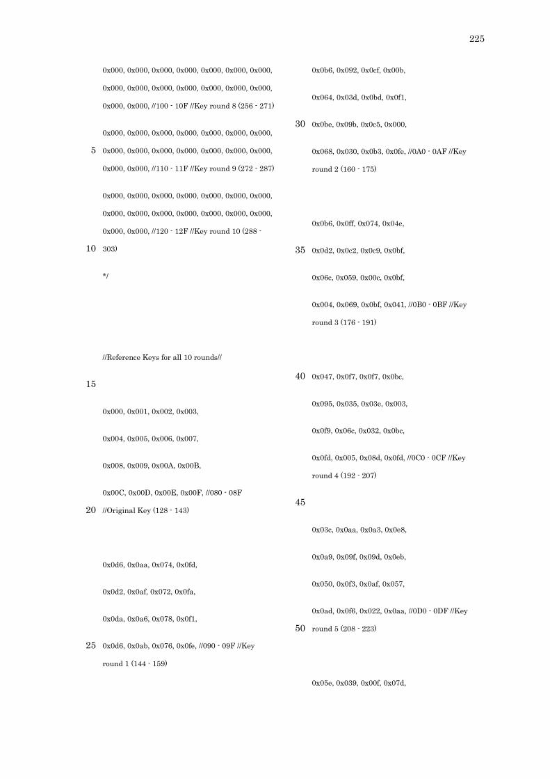
225
0x000, 0x000, 0x000, 0x000, 0x000, 0x000, 0x000,
0x000, 0x000, 0x000, 0x000, 0x000, 0x000, 0x000,
0x000, 0x000, //100 - 10F //Key round 8 (256 - 271)
0x000, 0x000, 0x000, 0x000, 0x000, 0x000, 0x000,
0x000, 0x000, 0x000, 0x000, 0x000, 0x000, 0x000, 5
0x000, 0x000, //110 - 11F //Key round 9 (272 - 287)
0x000, 0x000, 0x000, 0x000, 0x000, 0x000, 0x000,
0x000, 0x000, 0x000, 0x000, 0x000, 0x000, 0x000,
0x000, 0x000, //120 - 12F //Key round 10 (288 -
303) 10
*/
//Reference Keys for all 10 rounds//
15
0x000, 0x001, 0x002, 0x003,
0x004, 0x005, 0x006, 0x007,
0x008, 0x009, 0x00A, 0x00B,
0x00C, 0x00D, 0x00E, 0x00F, //080 - 08F
//Original Key (128 - 143) 20
0x0d6, 0x0aa, 0x074, 0x0fd,
0x0d2, 0x0af, 0x072, 0x0fa,
0x0da, 0x0a6, 0x078, 0x0f1,
0x0d6, 0x0ab, 0x076, 0x0fe, //090 - 09F //Key 25
round 1 (144 - 159)
0x0b6, 0x092, 0x0cf, 0x00b,
0x064, 0x03d, 0x0bd, 0x0f1,
0x0be, 0x09b, 0x0c5, 0x000, 30
0x068, 0x030, 0x0b3, 0x0fe, //0A0 - 0AF //Key
round 2 (160 - 175)
0x0b6, 0x0ff, 0x074, 0x04e,
0x0d2, 0x0c2, 0x0c9, 0x0bf, 35
0x06c, 0x059, 0x00c, 0x0bf,
0x004, 0x069, 0x0bf, 0x041, //0B0 - 0BF //Key
round 3 (176 - 191)
0x047, 0x0f7, 0x0f7, 0x0bc, 40
0x095, 0x035, 0x03e, 0x003,
0x0f9, 0x06c, 0x032, 0x0bc,
0x0fd, 0x005, 0x08d, 0x0fd, //0C0 - 0CF //Key
round 4 (192 - 207)
45
0x03c, 0x0aa, 0x0a3, 0x0e8,
0x0a9, 0x09f, 0x09d, 0x0eb,
0x050, 0x0f3, 0x0af, 0x057,
0x0ad, 0x0f6, 0x022, 0x0aa, //0D0 - 0DF //Key
round 5 (208 - 223) 50
0x05e, 0x039, 0x00f, 0x07d,
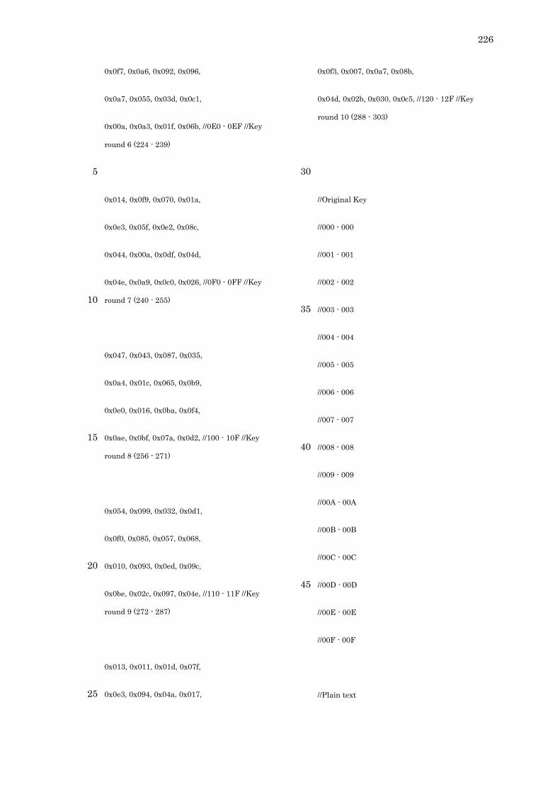
226
0x0f7, 0x0a6, 0x092, 0x096,
0x0a7, 0x055, 0x03d, 0x0c1,
0x00a, 0x0a3, 0x01f, 0x06b, //0E0 - 0EF //Key
round 6 (224 - 239)
5
0x014, 0x0f9, 0x070, 0x01a,
0x0e3, 0x05f, 0x0e2, 0x08c,
0x044, 0x00a, 0x0df, 0x04d,
0x04e, 0x0a9, 0x0c0, 0x026, //0F0 - 0FF //Key
round 7 (240 - 255) 10
0x047, 0x043, 0x087, 0x035,
0x0a4, 0x01c, 0x065, 0x0b9,
0x0e0, 0x016, 0x0ba, 0x0f4,
0x0ae, 0x0bf, 0x07a, 0x0d2, //100 - 10F //Key 15
round 8 (256 - 271)
0x054, 0x099, 0x032, 0x0d1,
0x0f0, 0x085, 0x057, 0x068,
0x010, 0x093, 0x0ed, 0x09c, 20
0x0be, 0x02c, 0x097, 0x04e, //110 - 11F //Key
round 9 (272 - 287)
0x013, 0x011, 0x01d, 0x07f,
0x0e3, 0x094, 0x04a, 0x017, 25
0x0f3, 0x007, 0x0a7, 0x08b,
0x04d, 0x02b, 0x030, 0x0c5, //120 - 12F //Key
round 10 (288 - 303)
30
//Original Key
//000 - 000
//001 - 001
//002 - 002
//003 - 003 35
//004 - 004
//005 - 005
//006 - 006
//007 - 007
//008 - 008 40
//009 - 009
//00A - 00A
//00B - 00B
//00C - 00C
//00D - 00D 45
//00E - 00E
//00F - 00F
//Plain text
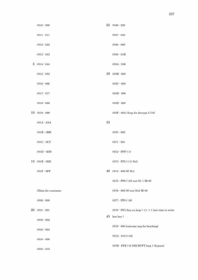
227
//010 - 000
//011 - 011
//012 - 022
//013 - 033
//014 - 044 5
//015 - 055
//016 - 066
//017 - 077
//018 - 088
//019 - 099 10
//01A - 0AA
//01B - 0BB
//01C - 0CC
//01D - 0DD
//01E - 0EE 15
//01F - 0FF
//Data for constants
//030 - 000
//031 - 001 20
//032 - 002
//033 - 004
//034 - 008
//035 - 010
//036 - 020 25
//037 - 040
//038 - 080
//039 - 01B
//03A - 036
//03B - 000 30
//03C - 000
//03D - 000
//03E - 000
//03F - 00A //loop for decrypt 2 (10)
35
//070 - 000
//071 - 001
//072 - FFF (-1)
//073 - FF5 (-11) Nr2
//074 - 009 (9) Nr1 40
//075 - FF6 (-10) test Nr 1 (R=9)
//076 - 008 (8) test Nr2 (R=9)
//077 - FF0 (-16)
//078 - FF5 (key.ex loop = 11 -> 1 last time to write
last key ) 45
//079 - 800 (extreme neg for braching)
//07A - 010 (+16)
//07B - FFE (-2) DECRYPT loop 1 (bypass)

228
//---------------KEY EXPANSION----------------//
//run 10 rounds of key expansion algorithm
0x000, 0x000, //304, 305 5
//move current key to key mem
0x400, 0x080, 0x000, //306
0x401, 0x081, 0x000,
0x402, 0x082, 0x000, 10
0x403, 0x083, 0x000,
0x404, 0x084, 0x000,
0x405, 0x085, 0x000,
0x406, 0x086, 0x000,
0x407, 0x087, 0x000, 15
0x408, 0x088, 0x000,
0x409, 0x089, 0x000,
0x40A, 0x08A, 0x000,
0x40B, 0x08B, 0x000,
0x40C, 0x08C, 0x000, 20
0x40D, 0x08D, 0x000,
0x40E, 0x08E, 0x000,
0x40F, 0x08F, 0x000, //353
//clear temp key var and ROT word 25
0x07C, 0x07C, 0x000, //354
0x07D, 0x07D, 0x000,
0x07E, 0x07E, 0x000,
0x07F, 0x07F, 0x000, //365
30
//Rot Word
0x40D, 0x07C, 0x000, //366
0x40E, 0x07D, 0x000,
0x40F, 0x07E, 0x000,
0x40C, 0x07F, 0x000, //377 35
//Sub word
0xC00, 0x07C, 0x000, //378
0xC00, 0x07D, 0x000,
0xC00, 0x07E, 0x000, 40
0xC00, 0x07F, 0x000, //389
//XOR RCon
//increment program + load RCON
0x072, 0x189, 0x000, // 390 - 392 45
//load Rcon (XOR to MSB key)
0x430, 0x07C, 0x000, // 393 - 395

229
5
10
15
20
25
30
35
40
45
50
55
60
65
70

230
5
10
15
20
25
30
//key gen
0x47C, 0x000, 0x000, //396
0x47D, 0x001, 0x000,
0x47E, 0x002, 0x000,
0x47F, 0x003, 0x000, 35
0x400, 0x004, 0x000,
0x401, 0x005, 0x000,
0x402, 0x006, 0x000,
0x403, 0x007, 0x000, 40
0x404, 0x008, 0x000,
0x405, 0x009, 0x000,
0x406, 0x00A, 0x000,
0x407, 0x00B, 0x000, 45
0x408, 0x00C, 0x000,
0x409, 0x00D, 0x000,
0x40A, 0x00E, 0x000,
0x40B, 0x00F, 0x000, // 443 50
//increment round key memory locations by 16
0x077, 0x133, 0x000, //444
0x077, 0x136, 0x000,
0x077, 0x139, 0x000, 55
0x077, 0x13C, 0x000,
0x077, 0x13F, 0x000,
0x077, 0x142, 0x000,
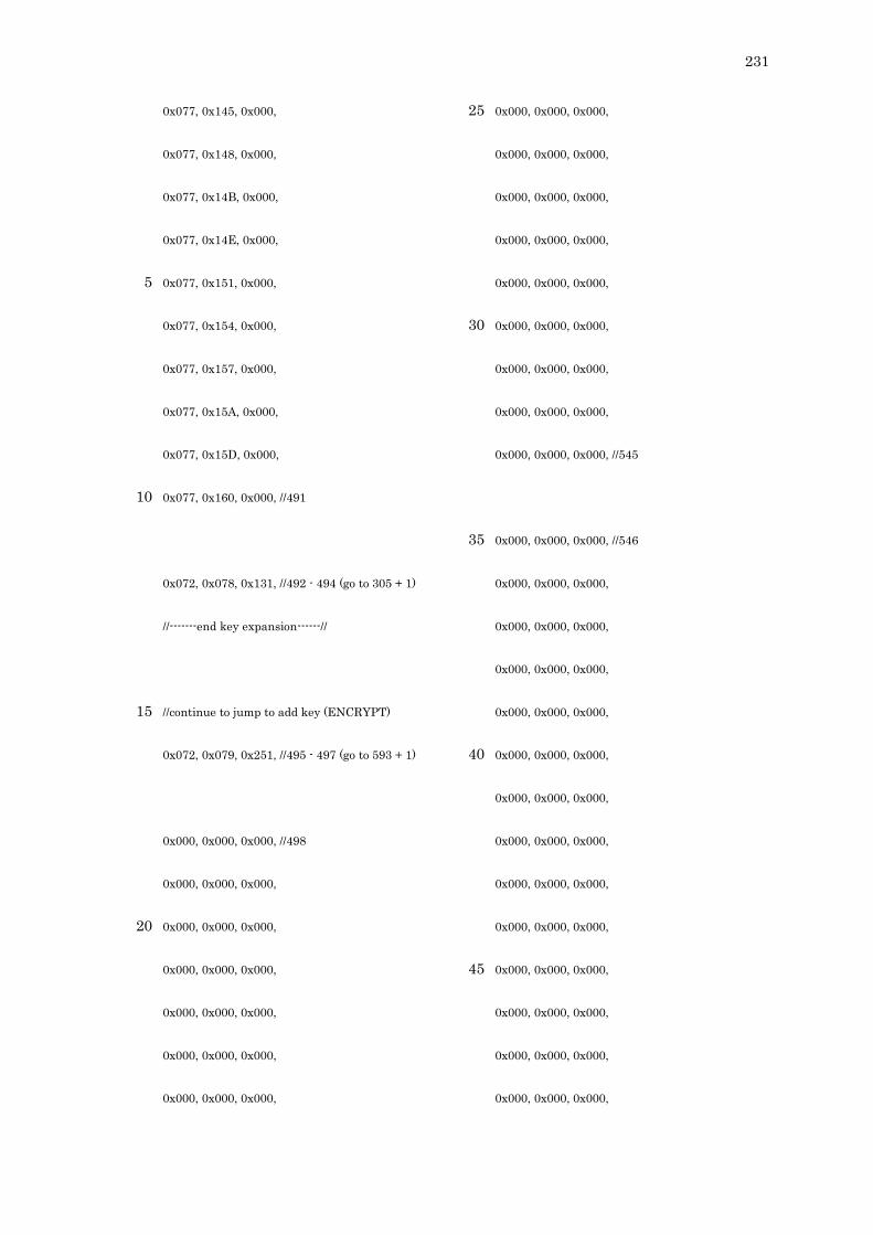
231
0x077, 0x145, 0x000,
0x077, 0x148, 0x000,
0x077, 0x14B, 0x000,
0x077, 0x14E, 0x000,
0x077, 0x151, 0x000, 5
0x077, 0x154, 0x000,
0x077, 0x157, 0x000,
0x077, 0x15A, 0x000,
0x077, 0x15D, 0x000,
0x077, 0x160, 0x000, //491 10
0x072, 0x078, 0x131, //492 - 494 (go to 305 + 1)
//-------end key expansion------//
//continue to jump to add key (ENCRYPT) 15
0x072, 0x079, 0x251, //495 - 497 (go to 593 + 1)
0x000, 0x000, 0x000, //498
0x000, 0x000, 0x000,
0x000, 0x000, 0x000, 20
0x000, 0x000, 0x000,
0x000, 0x000, 0x000,
0x000, 0x000, 0x000,
0x000, 0x000, 0x000,
0x000, 0x000, 0x000, 25
0x000, 0x000, 0x000,
0x000, 0x000, 0x000,
0x000, 0x000, 0x000,
0x000, 0x000, 0x000,
0x000, 0x000, 0x000, 30
0x000, 0x000, 0x000,
0x000, 0x000, 0x000,
0x000, 0x000, 0x000, //545
0x000, 0x000, 0x000, //546 35
0x000, 0x000, 0x000,
0x000, 0x000, 0x000,
0x000, 0x000, 0x000,
0x000, 0x000, 0x000,
0x000, 0x000, 0x000, 40
0x000, 0x000, 0x000,
0x000, 0x000, 0x000,
0x000, 0x000, 0x000,
0x000, 0x000, 0x000,
0x000, 0x000, 0x000, 45
0x000, 0x000, 0x000,
0x000, 0x000, 0x000,
0x000, 0x000, 0x000,
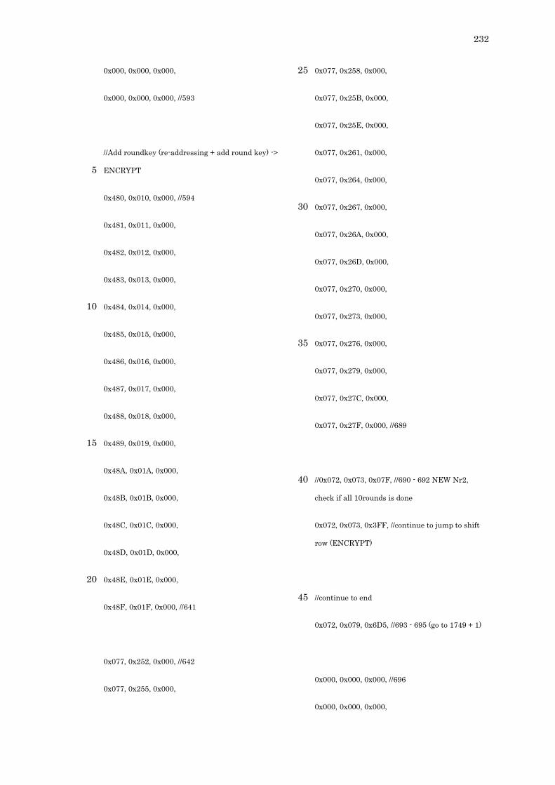
232
0x000, 0x000, 0x000,
0x000, 0x000, 0x000, //593
//Add roundkey (re-addressing + add round key) ->
ENCRYPT 5
0x480, 0x010, 0x000, //594
0x481, 0x011, 0x000,
0x482, 0x012, 0x000,
0x483, 0x013, 0x000,
0x484, 0x014, 0x000, 10
0x485, 0x015, 0x000,
0x486, 0x016, 0x000,
0x487, 0x017, 0x000,
0x488, 0x018, 0x000,
0x489, 0x019, 0x000, 15
0x48A, 0x01A, 0x000,
0x48B, 0x01B, 0x000,
0x48C, 0x01C, 0x000,
0x48D, 0x01D, 0x000,
0x48E, 0x01E, 0x000, 20
0x48F, 0x01F, 0x000, //641
0x077, 0x252, 0x000, //642
0x077, 0x255, 0x000,
0x077, 0x258, 0x000, 25
0x077, 0x25B, 0x000,
0x077, 0x25E, 0x000,
0x077, 0x261, 0x000,
0x077, 0x264, 0x000,
0x077, 0x267, 0x000, 30
0x077, 0x26A, 0x000,
0x077, 0x26D, 0x000,
0x077, 0x270, 0x000,
0x077, 0x273, 0x000,
0x077, 0x276, 0x000, 35
0x077, 0x279, 0x000,
0x077, 0x27C, 0x000,
0x077, 0x27F, 0x000, //689
//0x072, 0x073, 0x07F, //690 - 692 NEW Nr2, 40
check if all 10rounds is done
0x072, 0x073, 0x3FF, //continue to jump to shift
row (ENCRYPT)
//continue to end 45
0x072, 0x079, 0x6D5, //693 - 695 (go to 1749 + 1)
0x000, 0x000, 0x000, //696
0x000, 0x000, 0x000,

233
0x000, 0x000, 0x000,
0x000, 0x000, 0x000,
0x000, 0x000, 0x000,
0x000, 0x000, 0x000,
0x000, 0x000, 0x000, 5
0x000, 0x000, 0x000,
0x000, 0x000, 0x000,
0x000, 0x000, 0x000,
0x000, 0x000, 0x000,
0x000, 0x000, 0x000, 10
0x000, 0x000, 0x000,
0x000, 0x000, 0x000,
0x000, 0x000, 0x000,
0x000, 0x000, 0x000, //743
15
//Add roundkey (re-addressing + add round key) ->
DECRYPT
0x520, 0x040, 0x000, //744
0x521, 0x041, 0x000,
0x522, 0x042, 0x000, 20
0x523, 0x043, 0x000,
0x524, 0x044, 0x000,
0x525, 0x045, 0x000,
0x526, 0x046, 0x000,
0x527, 0x047, 0x000, 25
0x528, 0x048, 0x000,
0x529, 0x049, 0x000,
0x52A, 0x04A, 0x000,
0x52B, 0x04B, 0x000,
0x52C, 0x04C, 0x000, 30
0x52D, 0x04D, 0x000,
0x52E, 0x04E, 0x000,
0x52F, 0x04F, 0x000, //791
0x07A, 0x2E8, 0x000, //792 35
0x07A, 0x2EB, 0x000,
0x07A, 0x2EE, 0x000,
0x07A, 0x2F1, 0x000,
0x07A, 0x2F4, 0x000,
0x07A, 0x2F7, 0x000, 40
0x07A, 0x2FA, 0x000,
0x07A, 0x2FD, 0x000,
0x07A, 0x300, 0x000,
0x07A, 0x303, 0x000,
0x07A, 0x306, 0x000, 45
0x07A, 0x309, 0x000,
0x07A, 0x30C, 0x000,
0x07A, 0x30F, 0x000,
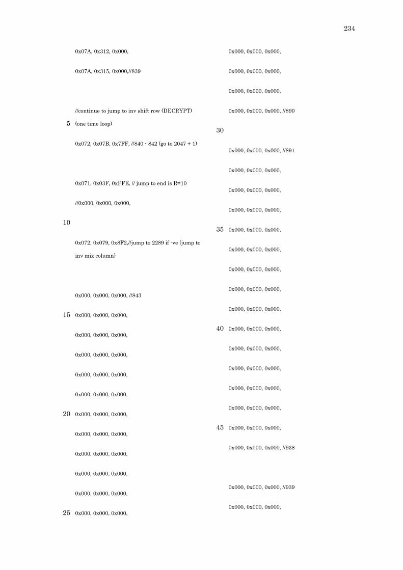
234
0x07A, 0x312, 0x000,
0x07A, 0x315, 0x000,//839
//continue to jump to inv shift row (DECRYPT)
(one time loop) 5
0x072, 0x07B, 0x7FF, //840 - 842 (go to 2047 + 1)
0x071, 0x03F, 0xFFE, // jump to end is R=10
//0x000, 0x000, 0x000,
10
0x072, 0x079, 0x8F2,//jump to 2289 if -ve (jump to
inv mix column)
0x000, 0x000, 0x000, //843
0x000, 0x000, 0x000, 15
0x000, 0x000, 0x000,
0x000, 0x000, 0x000,
0x000, 0x000, 0x000,
0x000, 0x000, 0x000,
0x000, 0x000, 0x000, 20
0x000, 0x000, 0x000,
0x000, 0x000, 0x000,
0x000, 0x000, 0x000,
0x000, 0x000, 0x000,
0x000, 0x000, 0x000, 25
0x000, 0x000, 0x000,
0x000, 0x000, 0x000,
0x000, 0x000, 0x000,
0x000, 0x000, 0x000, //890
30
0x000, 0x000, 0x000, //891
0x000, 0x000, 0x000,
0x000, 0x000, 0x000,
0x000, 0x000, 0x000,
0x000, 0x000, 0x000, 35
0x000, 0x000, 0x000,
0x000, 0x000, 0x000,
0x000, 0x000, 0x000,
0x000, 0x000, 0x000,
0x000, 0x000, 0x000, 40
0x000, 0x000, 0x000,
0x000, 0x000, 0x000,
0x000, 0x000, 0x000,
0x000, 0x000, 0x000,
0x000, 0x000, 0x000, 45
0x000, 0x000, 0x000, //938
0x000, 0x000, 0x000, //939
0x000, 0x000, 0x000,
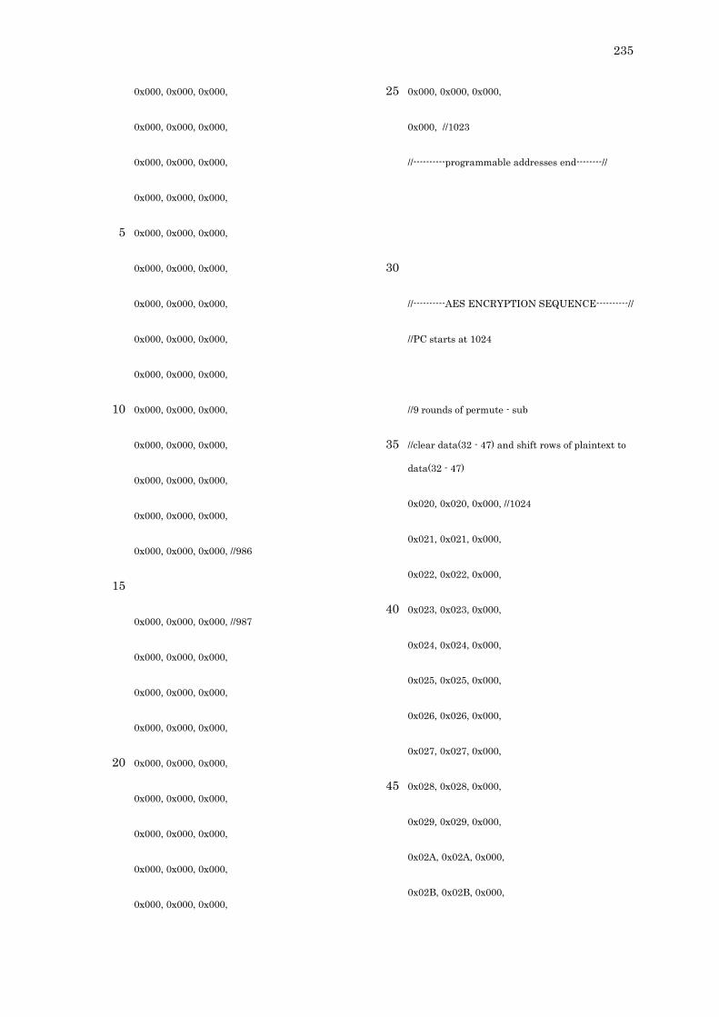
235
0x000, 0x000, 0x000,
0x000, 0x000, 0x000,
0x000, 0x000, 0x000,
0x000, 0x000, 0x000,
0x000, 0x000, 0x000, 5
0x000, 0x000, 0x000,
0x000, 0x000, 0x000,
0x000, 0x000, 0x000,
0x000, 0x000, 0x000,
0x000, 0x000, 0x000, 10
0x000, 0x000, 0x000,
0x000, 0x000, 0x000,
0x000, 0x000, 0x000,
0x000, 0x000, 0x000, //986
15
0x000, 0x000, 0x000, //987
0x000, 0x000, 0x000,
0x000, 0x000, 0x000,
0x000, 0x000, 0x000,
0x000, 0x000, 0x000, 20
0x000, 0x000, 0x000,
0x000, 0x000, 0x000,
0x000, 0x000, 0x000,
0x000, 0x000, 0x000,
0x000, 0x000, 0x000, 25
0x000, //1023
//----------programmable addresses end--------//
30
//----------AES ENCRYPTION SEQUENCE----------//
//PC starts at 1024
//9 rounds of permute - sub
//clear data(32 - 47) and shift rows of plaintext to 35
data(32 - 47)
0x020, 0x020, 0x000, //1024
0x021, 0x021, 0x000,
0x022, 0x022, 0x000,
0x023, 0x023, 0x000, 40
0x024, 0x024, 0x000,
0x025, 0x025, 0x000,
0x026, 0x026, 0x000,
0x027, 0x027, 0x000,
0x028, 0x028, 0x000, 45
0x029, 0x029, 0x000,
0x02A, 0x02A, 0x000,
0x02B, 0x02B, 0x000,

236
0x02C, 0x02C, 0x000,
0x02D, 0x02D, 0x000,
0x02E, 0x02E, 0x000,
0x02F, 0x02F, 0x000, // (96)
5
0x410, 0x020, 0x000,
0x415, 0x021, 0x000,
0x41A, 0x022, 0x000,
0x41F, 0x023, 0x000,
0x414, 0x024, 0x000, 10
0x419, 0x025, 0x000,
0x41E, 0x026, 0x000,
0x413, 0x027, 0x000,
0x418, 0x028, 0x000,
0x41D, 0x029, 0x000, 15
0x412, 0x02A, 0x000,
0x417, 0x02B, 0x000,
0x41C, 0x02C, 0x000,
0x411, 0x02D, 0x000,
0x416, 0x02E, 0x000, 20
0x41B, 0x02F, 0x000, // 1119
//sub bytes (stored in 010 - 01F)
0xC00, 0x020, 0x000, //1120
0xC00, 0x021, 0x000, 25
0xC00, 0x022, 0x000,
0xC00, 0x023, 0x000,
0xC00, 0x024, 0x000,
0xC00, 0x025, 0x000,
0xC00, 0x026, 0x000, 30
0xC00, 0x027, 0x000,
0xC00, 0x028, 0x000,
0xC00, 0x029, 0x000,
0xC00, 0x02A, 0x000,
0xC00, 0x02B, 0x000, 35
0xC00, 0x02C, 0x000,
0xC00, 0x02D, 0x000,
0xC00, 0x02E, 0x000,
0xC00, 0x02F, 0x000, // 1167
40
//check that all 9 round completed
0x071, 0x074, 0x672, // 1168 - 1170 (go to end of
mix column for last round of add key)
45
//mix column of data(32 - 47) and stored in
data(32 - 47)
//clear location(080 - 08F & 090 - 09F) and move
data to location(080 - 08F & 090 - 09F)
237
0x050, 0x050, 0x000, //1171
0x051, 0x051, 0x000,
0x052, 0x052, 0x000,
0x053, 0x053, 0x000,
0x054, 0x054, 0x000, 5
0x055, 0x055, 0x000,
0x056, 0x056, 0x000,
0x057, 0x057, 0x000,
0x058, 0x058, 0x000, //(48)
0x059, 0x059, 0x000, 10
0x05A, 0x05A, 0x000,
0x05B, 0x05B, 0x000,
0x05C, 0x05C, 0x000,
0x05D, 0x05D, 0x000,
0x05E, 0x05E, 0x000, 15
0x05F, 0x05F, 0x000, //1218
0x060, 0x060, 0x000, //1219
0x061, 0x061, 0x000,
0x062, 0x062, 0x000, 20
0x063, 0x063, 0x000,
0x064, 0x064, 0x000,
0x065, 0x065, 0x000,
0x066, 0x066, 0x000,
0x067, 0x067, 0x000, //(48) 25
0x068, 0x068, 0x000,
0x069, 0x069, 0x000,
0x06A, 0x06A, 0x000,
0x06B, 0x06B, 0x000,
0x06C, 0x06C, 0x000, 30
0x06D, 0x06D, 0x000,
0x06E, 0x06E, 0x000,
0x06F, 0x06F, 0x000, //1266
0x420, 0x050, 0x000, //1267 35
0x421, 0x051, 0x000,
0x422, 0x052, 0x000,
0x423, 0x053, 0x000,
0x424, 0x054, 0x000,
0x425, 0x055, 0x000, 40
0x426, 0x056, 0x000,
0x427, 0x057, 0x000,
0x428, 0x058, 0x000, //(48)
0x429, 0x059, 0x000,
0x42A, 0x05A, 0x000, 45
0x42B, 0x05B, 0x000,
0x42C, 0x05C, 0x000,
0x42D, 0x05D, 0x000,
238
0x42E, 0x05E, 0x000,
0x42F, 0x05F, 0x000, //1314
0x420, 0x060, 0x000, //1315
0x421, 0x061, 0x000, 5
0x422, 0x062, 0x000,
0x423, 0x063, 0x000,
0x424, 0x064, 0x000,
0x425, 0x065, 0x000,
0x426, 0x066, 0x000, //(48) 10
0x427, 0x067, 0x000,
0x428, 0x068, 0x000,
0x429, 0x069, 0x000,
0x42A, 0x06A, 0x000,
0x42B, 0x06B, 0x000, 15
0x42C, 0x06C, 0x000,
0x42D, 0x06D, 0x000,
0x42E, 0x06E, 0x000,
0x42F, 0x06F, 0x000, //1362
20
//column0
0x423, 0x050, 0x000, // 1363
0x420, 0x051, 0x000, //
0x421, 0x052, 0x000, //
0x422, 0x053, 0x000, // 25
0x452, 0x060, 0x000, //
0x453, 0x061, 0x000, //
0x450, 0x062, 0x000, //
0x451, 0x063, 0x000, // 30
0x800, 0x050, 0x000,
0x800, 0x051, 0x000,
0x800, 0x052, 0x000,
0x800, 0x053, 0x000, // 35
0x450, 0x060, 0x000,
0x451, 0x061, 0x000,
0x452, 0x062, 0x000,
0x453, 0x063, 0x000, // (72) 40
0x020, 0x020, 0x000,
0x021, 0x021, 0x000,
0x022, 0x022, 0x000,
0x023, 0x023, 0x000, // 45
0x461, 0x020, 0x000,
0x462, 0x021, 0x000,

239
0x463, 0x022, 0x000,
0x460, 0x023, 0x000, // 1434
//column1
0x427, 0x054, 0x000, //1435 5
0x424, 0x055, 0x000,
0x425, 0x056, 0x000,
0x426, 0x057, 0x000, //
0x456, 0x064, 0x000, 10
0x457, 0x065, 0x000,
0x454, 0x066, 0x000,
0x455, 0x067, 0x000, //
0x800, 0x054, 0x000, 15
0x800, 0x055, 0x000,
0x800, 0x056, 0x000,
0x800, 0x057, 0x000, //
0x454, 0x064, 0x000, 20
0x455, 0x065, 0x000,
0x456, 0x066, 0x000,
0x457, 0x067, 0x000, //
0x024, 0x024, 0x000, 25
0x025, 0x025, 0x000,
0x026, 0x026, 0x000,
0x027, 0x027, 0x000, //
0x465, 0x024, 0x000, 30
0x466, 0x025, 0x000,
0x467, 0x026, 0x000,
0x464, 0x027, 0x000, // 1506
35
//column2
0x42B, 0x058, 0x000, //1507
0x428, 0x059, 0x000,
0x429, 0x05A, 0x000,
0x42A, 0x05B, 0x000, 40
0x45A, 0x068, 0x000,
0x45B, 0x069, 0x000,
0x458, 0x06A, 0x000,
0x459, 0x06B, 0x000, 45
0x800, 0x058, 0x000,
0x800, 0x059, 0x000,

240
0x800, 0x05A, 0x000,
0x800, 0x05B, 0x000,
0x458, 0x068, 0x000,
0x459, 0x069, 0x000, 5
0x45A, 0x06A, 0x000,
0x45B, 0x06B, 0x000,
0x028, 0x028, 0x000,
0x029, 0x029, 0x000, 10
0x02A, 0x02A, 0x000,
0x02B, 0x02B, 0x000,
0x469, 0x028, 0x000,
0x46A, 0x029, 0x000, 15
0x46B, 0x02A, 0x000,
0x468, 0x02B, 0x000, //1578
//column3 20
0x42F, 0x05C, 0x000, //1579
0x42C, 0x05D, 0x000,
0x42D, 0x05E, 0x000,
0x42E, 0x05F, 0x000,
25
0x45E, 0x06C, 0x000,
0x45F, 0x06D, 0x000,
0x45C, 0x06E, 0x000,
0x45D, 0x06F, 0x000,
30
0x800, 0x05C, 0x000,
0x800, 0x05D, 0x000,
0x800, 0x05E, 0x000,
0x800, 0x05F, 0x000,
35
0x45C, 0x06C, 0x000,
0x45D, 0x06D, 0x000,
0x45E, 0x06E, 0x000,
0x45F, 0x06F, 0x000,
40
0x02C, 0x02C, 0x000,
0x02D, 0x02D, 0x000,
0x02E, 0x02E, 0x000,
0x02F, 0x02F, 0x000,
45
0x46D, 0x02C, 0x000,
0x46E, 0x02D, 0x000,
0x46F, 0x02E, 0x000,
241
0x46C, 0x02F, 0x000, // 1650
//clear 010 = 01F
0x010, 0x010, 0x000, //1651
0x011, 0x011, 0x000, 5
0x012, 0x012, 0x000,
0x013, 0x013, 0x000,
0x014, 0x014, 0x000,
0x015, 0x015, 0x000,
0x016, 0x016, 0x000, 10
0x017, 0x017, 0x000, //(48)
0x018, 0x018, 0x000,
0x019, 0x019, 0x000,
0x01A, 0x01A, 0x000,
0x01B, 0x01B, 0x000, 15
0x01C, 0x01C, 0x000,
0x01D, 0x01D, 0x000,
0x01E, 0x01E, 0x000,
0x01F, 0x01F, 0x000, //1698
20
//move the mixcolumn result from 020 - 02f to 010
- 01f
0x420, 0x010, 0x000, //1699
0x421, 0x011, 0x000,
0x422, 0x012, 0x000, 25
0x423, 0x013, 0x000,
0x424, 0x014, 0x000,
0x425, 0x015, 0x000,
0x426, 0x016, 0x000,
0x427, 0x017, 0x000, 30
0x428, 0x018, 0x000,
0x429, 0x019, 0x000,
0x42A, 0x01A, 0x000,
0x42B, 0x01B, 0x000,
0x42C, 0x01C, 0x000, 35
0x42D, 0x01D, 0x000,
0x42E, 0x01E, 0x000,
0x42F, 0x01F, 0x000, //1746
0x072, 0x079, 0x251, //1747 - 1749 (back to add 40
key ENCRYPT)
//move the encrypted result to 040 - 04f for
decryption
0x410, 0x040, 0x000, //1750 45
0x411, 0x041, 0x000,
0x412, 0x042, 0x000,
0x413, 0x043, 0x000,
0x414, 0x044, 0x000,
242
0x415, 0x045, 0x000,
0x416, 0x046, 0x000,
0x417, 0x047, 0x000,
0x418, 0x048, 0x000,
0x419, 0x049, 0x000, 5
0x41A, 0x04A, 0x000,
0x41B, 0x04B, 0x000,
0x41C, 0x04C, 0x000,
0x41D, 0x04D, 0x000,
0x41E, 0x04E, 0x000, 10
0x41F, 0x04F, 0x000, //1797
0x072, 0x079, 0xFFE, //1798 - 1800 (END OF
ENCRYPT)
//0x000, 0x000, 0x000, //1798 - 1800 (END OF 15
ENCRYPT)
0x000, 0x000, 0x000, //1801
0x000, 0x000, 0x000,
0x000, 0x000, 0x000, 20
0x000, 0x000, 0x000,
0x000, 0x000, 0x000,
0x000, 0x000, 0x000,
0x000, 0x000, 0x000,
0x000, 0x000, 0x000, 25
0x000, 0x000, 0x000,
0x000, 0x000, 0x000,
0x000, 0x000, 0x000,
0x000, 0x000, 0x000,
0x000, 0x000, 0x000, 30
0x000, 0x000, 0x000,
0x000, 0x000, 0x000,
0x000, 0x000, 0x000, //1848
0x000, 0x000, 0x000, //1849 35
0x000, 0x000, 0x000,
0x000, 0x000, 0x000,
0x000, 0x000, 0x000,
0x000, 0x000, 0x000,
0x000, 0x000, 0x000, 40
0x000, 0x000, 0x000,
0x000, 0x000, 0x000,
0x000, 0x000, 0x000,
0x000, 0x000, 0x000,
0x000, 0x000, 0x000, 45
0x000, 0x000, 0x000,
0x000, 0x000, 0x000,
0x000, 0x000, 0x000,
0x000, 0x000, 0x000,

243
0x000, 0x000, 0x000, //1896
0x000, 0x000, 0x000, //1897
0x000, 0x000, 0x000,
0x000, 0x000, 0x000, 5
0x000, 0x000, 0x000,
0x000, 0x000, 0x000,
0x000, 0x000, 0x000,
0x000, 0x000, 0x000,
0x000, 0x000, 0x000, 10
0x000, 0x000, 0x000,
0x000, 0x000, 0x000,
0x000, 0x000, 0x000,
0x000, 0x000, 0x000,
0x000, 0x000, 0x000, 15
0x000, 0x000, 0x000,
0x000, 0x000, 0x000,
0x000, 0x000, 0x000, //1944
0x000, 0x000, 0x000, //1945 20
0x000, 0x000, 0x000,
0x000, 0x000, 0x000,
0x000, 0x000, 0x000,
0x000, 0x000, 0x000,
0x000, 0x000, 0x000, 25
0x000, 0x000, 0x000,
0x000, 0x000, 0x000,
0x000, 0x000, 0x000,
0x000, 0x000, 0x000,
0x000, 0x000, 0x000, 30
0x000, 0x000, 0x000,
0x000, 0x000, 0x000,
0x000, 0x000, 0x000,
0x000, 0x000, 0x000,
0x000, 0x000, 0x000, //1992 35
0x000, 0x000, 0x000, //1993
0x000, 0x000, 0x000,
0x000, 0x000, 0x000,
0x000, 0x000, 0x000, 40
0x000, 0x000, 0x000,
0x000, 0x000, 0x000,
0x000, 0x000, 0x000,
0x000, 0x000, 0x000,
0x000, 0x000, 0x000, 45
0x000, 0x000, 0x000,
0x000, 0x000, 0x000,
0x000, 0x000, 0x000,
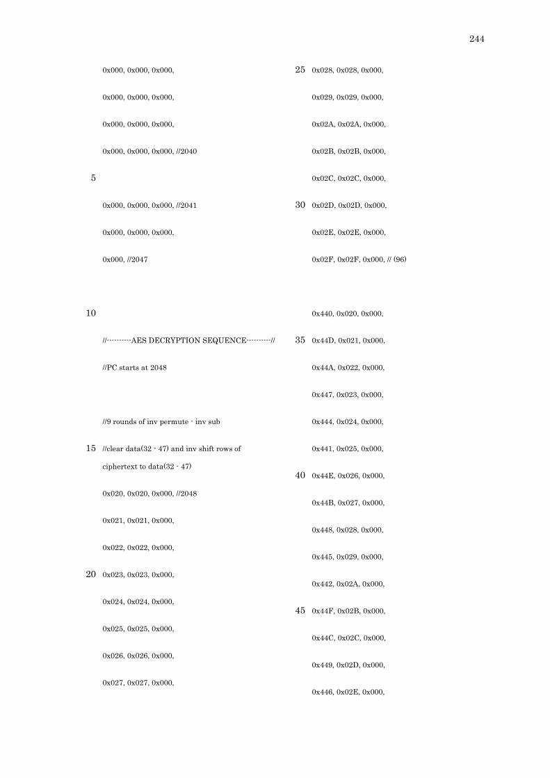
244
0x000, 0x000, 0x000,
0x000, 0x000, 0x000,
0x000, 0x000, 0x000,
0x000, 0x000, 0x000, //2040
5
0x000, 0x000, 0x000, //2041
0x000, 0x000, 0x000,
0x000, //2047
10
//----------AES DECRYPTION SEQUENCE----------//
//PC starts at 2048
//9 rounds of inv permute - inv sub
//clear data(32 - 47) and inv shift rows of 15
ciphertext to data(32 - 47)
0x020, 0x020, 0x000, //2048
0x021, 0x021, 0x000,
0x022, 0x022, 0x000,
0x023, 0x023, 0x000, 20
0x024, 0x024, 0x000,
0x025, 0x025, 0x000,
0x026, 0x026, 0x000,
0x027, 0x027, 0x000,
0x028, 0x028, 0x000, 25
0x029, 0x029, 0x000,
0x02A, 0x02A, 0x000,
0x02B, 0x02B, 0x000,
0x02C, 0x02C, 0x000,
0x02D, 0x02D, 0x000, 30
0x02E, 0x02E, 0x000,
0x02F, 0x02F, 0x000, // (96)
0x440, 0x020, 0x000,
0x44D, 0x021, 0x000, 35
0x44A, 0x022, 0x000,
0x447, 0x023, 0x000,
0x444, 0x024, 0x000,
0x441, 0x025, 0x000,
0x44E, 0x026, 0x000, 40
0x44B, 0x027, 0x000,
0x448, 0x028, 0x000,
0x445, 0x029, 0x000,
0x442, 0x02A, 0x000,
0x44F, 0x02B, 0x000, 45
0x44C, 0x02C, 0x000,
0x449, 0x02D, 0x000,
0x446, 0x02E, 0x000,

245
0x443, 0x02F, 0x000, // 2143
//sub bytes (stored in 010 - 01F)
0xC00, 0x020, 0x000, //2144
0xC00, 0x021, 0x000, 5
0xC00, 0x022, 0x000,
0xC00, 0x023, 0x000,
0xC00, 0x024, 0x000,
0xC00, 0x025, 0x000,
0xC00, 0x026, 0x000, 10
0xC00, 0x027, 0x000,
0xC00, 0x028, 0x000,
0xC00, 0x029, 0x000,
0xC00, 0x02A, 0x000,
0xC00, 0x02B, 0x000, 15
0xC00, 0x02C, 0x000,
0xC00, 0x02D, 0x000,
0xC00, 0x02E, 0x000,
0xC00, 0x02F, 0x000, // 2191
20
0x040, 0x040, 0x000, //2192
0x041, 0x041, 0x000,
0x042, 0x042, 0x000,
0x043, 0x043, 0x000,
0x044, 0x044, 0x000, 25
0x045, 0x045, 0x000,
0x046, 0x046, 0x000,
0x047, 0x047, 0x000,
0x048, 0x048, 0x000,
0x049, 0x049, 0x000, 30
0x04A, 0x04A, 0x000,
0x04B, 0x04B, 0x000,
0x04C, 0x04C, 0x000,
0x04D, 0x04D, 0x000,
0x04E, 0x04E, 0x000, 35
0x04F, 0x04F, 0x000, // (96)
0x420, 0x040, 0x000,
0x421, 0x041, 0x000,
0x422, 0x042, 0x000, 40
0x423, 0x043, 0x000,
0x424, 0x044, 0x000,
0x425, 0x045, 0x000,
0x426, 0x046, 0x000,
0x427, 0x047, 0x000, 45
0x428, 0x048, 0x000,
0x429, 0x049, 0x000,
0x42A, 0x04A, 0x000,
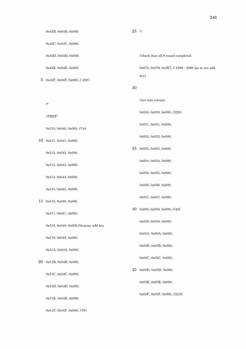
246
0x42B, 0x04B, 0x000,
0x42C, 0x04C, 0x000,
0x42D, 0x04D, 0x000,
0x42E, 0x04E, 0x000,
0x42F, 0x04F, 0x000, // 2287 5
/*
//TEST!
0x510, 0x040, 0x000, //744
0x511, 0x041, 0x000, 10
0x512, 0x042, 0x000,
0x513, 0x043, 0x000,
0x514, 0x044, 0x000,
0x515, 0x045, 0x000,
0x516, 0x046, 0x000, 15
0x517, 0x047, 0x000,
0x518, 0x048, 0x000,//dummy add key
0x519, 0x049, 0x000,
0x51A, 0x04A, 0x000,
0x51B, 0x04B, 0x000, 20
0x51C, 0x04C, 0x000,
0x51D, 0x04D, 0x000,
0x51E, 0x04E, 0x000,
0x51F, 0x04F, 0x000, //791
*/ 25
//check that all 9 round completed
0x072, 0x079, 0x2E7, // 2288 - 2290 (go to inv add
key)
30
//inv mix column
0x050, 0x050, 0x000, //2291
0x051, 0x051, 0x000,
0x052, 0x052, 0x000,
0x053, 0x053, 0x000, 35
0x054, 0x054, 0x000,
0x055, 0x055, 0x000,
0x056, 0x056, 0x000,
0x057, 0x057, 0x000,
0x058, 0x058, 0x000, //(48) 40
0x059, 0x059, 0x000,
0x05A, 0x05A, 0x000,
0x05B, 0x05B, 0x000,
0x05C, 0x05C, 0x000,
0x05D, 0x05D, 0x000, 45
0x05E, 0x05E, 0x000,
0x05F, 0x05F, 0x000, //2238
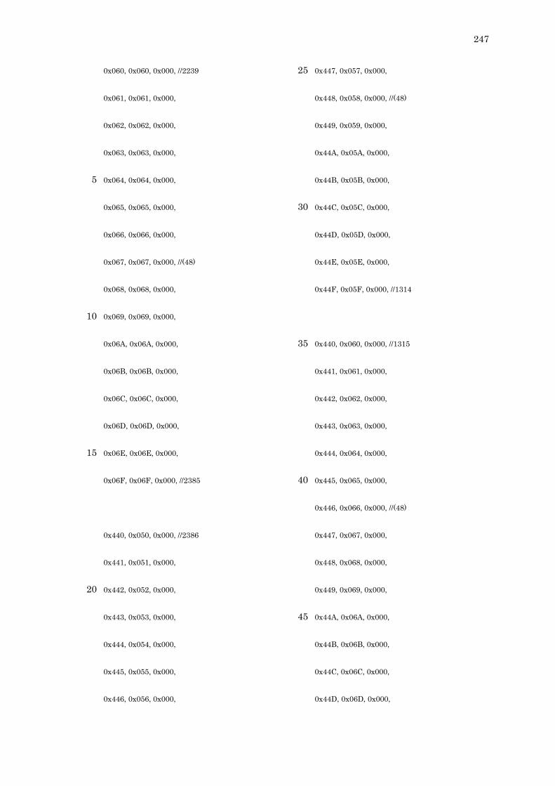
247
0x060, 0x060, 0x000, //2239
0x061, 0x061, 0x000,
0x062, 0x062, 0x000,
0x063, 0x063, 0x000,
0x064, 0x064, 0x000, 5
0x065, 0x065, 0x000,
0x066, 0x066, 0x000,
0x067, 0x067, 0x000, //(48)
0x068, 0x068, 0x000,
0x069, 0x069, 0x000, 10
0x06A, 0x06A, 0x000,
0x06B, 0x06B, 0x000,
0x06C, 0x06C, 0x000,
0x06D, 0x06D, 0x000,
0x06E, 0x06E, 0x000, 15
0x06F, 0x06F, 0x000, //2385
0x440, 0x050, 0x000, //2386
0x441, 0x051, 0x000,
0x442, 0x052, 0x000, 20
0x443, 0x053, 0x000,
0x444, 0x054, 0x000,
0x445, 0x055, 0x000,
0x446, 0x056, 0x000,
0x447, 0x057, 0x000, 25
0x448, 0x058, 0x000, //(48)
0x449, 0x059, 0x000,
0x44A, 0x05A, 0x000,
0x44B, 0x05B, 0x000,
0x44C, 0x05C, 0x000, 30
0x44D, 0x05D, 0x000,
0x44E, 0x05E, 0x000,
0x44F, 0x05F, 0x000, //1314
0x440, 0x060, 0x000, //1315 35
0x441, 0x061, 0x000,
0x442, 0x062, 0x000,
0x443, 0x063, 0x000,
0x444, 0x064, 0x000,
0x445, 0x065, 0x000, 40
0x446, 0x066, 0x000, //(48)
0x447, 0x067, 0x000,
0x448, 0x068, 0x000,
0x449, 0x069, 0x000,
0x44A, 0x06A, 0x000, 45
0x44B, 0x06B, 0x000,
0x44C, 0x06C, 0x000,
0x44D, 0x06D, 0x000,
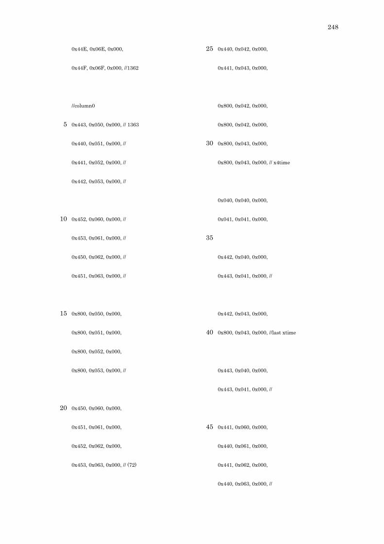
248
0x44E, 0x06E, 0x000,
0x44F, 0x06F, 0x000, //1362
//column0
0x443, 0x050, 0x000, // 1363 5
0x440, 0x051, 0x000, //
0x441, 0x052, 0x000, //
0x442, 0x053, 0x000, //
0x452, 0x060, 0x000, // 10
0x453, 0x061, 0x000, //
0x450, 0x062, 0x000, //
0x451, 0x063, 0x000, //
0x800, 0x050, 0x000, 15
0x800, 0x051, 0x000,
0x800, 0x052, 0x000,
0x800, 0x053, 0x000, //
0x450, 0x060, 0x000, 20
0x451, 0x061, 0x000,
0x452, 0x062, 0x000,
0x453, 0x063, 0x000, // (72)
0x440, 0x042, 0x000, 25
0x441, 0x043, 0x000,
0x800, 0x042, 0x000,
0x800, 0x042, 0x000,
0x800, 0x043, 0x000, 30
0x800, 0x043, 0x000, // x4time
0x040, 0x040, 0x000,
0x041, 0x041, 0x000,
35
0x442, 0x040, 0x000,
0x443, 0x041, 0x000, //
0x442, 0x043, 0x000,
0x800, 0x043, 0x000, //last xtime 40
0x443, 0x040, 0x000,
0x443, 0x041, 0x000, //
0x441, 0x060, 0x000, 45
0x440, 0x061, 0x000,
0x441, 0x062, 0x000,
0x440, 0x063, 0x000, //

249
0x040, 0x040, 0x000,
0x041, 0x041, 0x000,
0x042, 0x042, 0x000,
0x043, 0x043, 0x000, // 5
0x461, 0x040, 0x000,
0x462, 0x041, 0x000,
0x463, 0x042, 0x000,
0x460, 0x043, 0x000, // 1434 10
//column1
0x447, 0x054, 0x000, //1435
0x444, 0x055, 0x000,
0x445, 0x056, 0x000, 15
0x446, 0x057, 0x000, //
0x456, 0x064, 0x000,
0x457, 0x065, 0x000,
0x454, 0x066, 0x000, 20
0x455, 0x067, 0x000, //
0x800, 0x054, 0x000,
0x800, 0x055, 0x000,
0x800, 0x056, 0x000, 25
0x800, 0x057, 0x000, //
0x454, 0x064, 0x000,
0x455, 0x065, 0x000,
0x456, 0x066, 0x000, 30
0x457, 0x067, 0x000, //
0x444, 0x046, 0x000,
0x445, 0x047, 0x000,
35
0x800, 0x046, 0x000,
0x800, 0x046, 0x000,
0x800, 0x047, 0x000,
0x800, 0x047, 0x000, // x4time
40
0x044, 0x044, 0x000,
0x045, 0x045, 0x000,
0x446, 0x044, 0x000,
0x447, 0x045, 0x000, // 45
0x446, 0x047, 0x000,
0x800, 0x047, 0x000, //last xtime

250
0x447, 0x044, 0x000,
0x447, 0x045, 0x000, //
0x445, 0x064, 0x000, 5
0x444, 0x065, 0x000,
0x445, 0x066, 0x000,
0x444, 0x067, 0x000, //
0x044, 0x044, 0x000, 10
0x045, 0x045, 0x000,
0x046, 0x046, 0x000,
0x047, 0x047, 0x000, //
0x465, 0x044, 0x000, 15
0x466, 0x045, 0x000,
0x467, 0x046, 0x000,
0x464, 0x047, 0x000, // 1506
20
//column2
0x44B, 0x058, 0x000, //1507
0x448, 0x059, 0x000,
0x449, 0x05A, 0x000,
0x44A, 0x05B, 0x000, 25
0x45A, 0x068, 0x000,
0x45B, 0x069, 0x000,
0x458, 0x06A, 0x000,
0x459, 0x06B, 0x000, 30
0x800, 0x058, 0x000,
0x800, 0x059, 0x000,
0x800, 0x05A, 0x000,
0x800, 0x05B, 0x000, 35
0x458, 0x068, 0x000,
0x459, 0x069, 0x000,
0x45A, 0x06A, 0x000,
0x45B, 0x06B, 0x000, 40
0x448, 0x04A, 0x000,
0x449, 0x04B, 0x000,
0x800, 0x04A, 0x000, 45
0x800, 0x04A, 0x000,
0x800, 0x04B, 0x000,
0x800, 0x04B, 0x000, // x4time

251
0x048, 0x048, 0x000,
0x049, 0x049, 0x000,
0x44A, 0x048, 0x000, 5
0x44B, 0x049, 0x000, //
0x44A, 0x04B, 0x000,
0x800, 0x04B, 0x000, //last xtime
10
0x44B, 0x048, 0x000,
0x44B, 0x049, 0x000, //
0x449, 0x068, 0x000,
0x448, 0x069, 0x000, 15
0x449, 0x06A, 0x000,
0x448, 0x06B, 0x000, //
0x048, 0x048, 0x000,
0x049, 0x049, 0x000, 20
0x04A, 0x04A, 0x000,
0x04B, 0x04B, 0x000,
0x469, 0x048, 0x000,
0x46A, 0x049, 0x000, 25
0x46B, 0x04A, 0x000,
0x468, 0x04B, 0x000, //1578
//column3 30
0x44F, 0x05C, 0x000, //1507
0x44C, 0x05D, 0x000,
0x44D, 0x05E, 0x000,
0x44E, 0x05F, 0x000,
35
0x45E, 0x06C, 0x000,
0x45F, 0x06D, 0x000,
0x45C, 0x06E, 0x000,
0x45D, 0x06F, 0x000,
40
0x800, 0x05C, 0x000,
0x800, 0x05D, 0x000,
0x800, 0x05E, 0x000,
0x800, 0x05F, 0x000,
45
0x45C, 0x06C, 0x000,
0x45D, 0x06D, 0x000,
0x45E, 0x06E, 0x000,
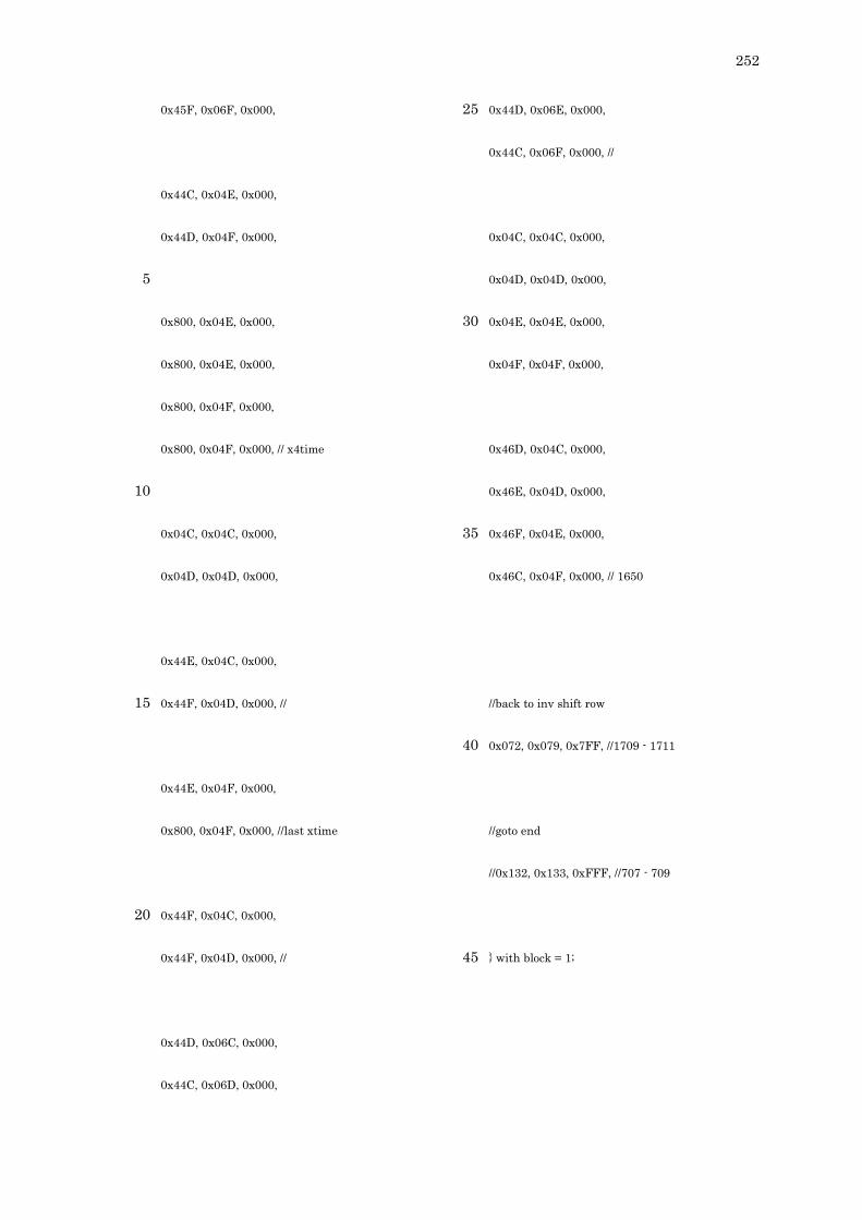
252
0x45F, 0x06F, 0x000,
0x44C, 0x04E, 0x000,
0x44D, 0x04F, 0x000,
5
0x800, 0x04E, 0x000,
0x800, 0x04E, 0x000,
0x800, 0x04F, 0x000,
0x800, 0x04F, 0x000, // x4time
10
0x04C, 0x04C, 0x000,
0x04D, 0x04D, 0x000,
0x44E, 0x04C, 0x000,
0x44F, 0x04D, 0x000, // 15
0x44E, 0x04F, 0x000,
0x800, 0x04F, 0x000, //last xtime
0x44F, 0x04C, 0x000, 20
0x44F, 0x04D, 0x000, //
0x44D, 0x06C, 0x000,
0x44C, 0x06D, 0x000,
0x44D, 0x06E, 0x000, 25
0x44C, 0x06F, 0x000, //
0x04C, 0x04C, 0x000,
0x04D, 0x04D, 0x000,
0x04E, 0x04E, 0x000, 30
0x04F, 0x04F, 0x000,
0x46D, 0x04C, 0x000,
0x46E, 0x04D, 0x000,
0x46F, 0x04E, 0x000, 35
0x46C, 0x04F, 0x000, // 1650
//back to inv shift row
0x072, 0x079, 0x7FF, //1709 - 1711 40
//goto end
//0x132, 0x133, 0xFFF, //707 - 709
} with block = 1; 45
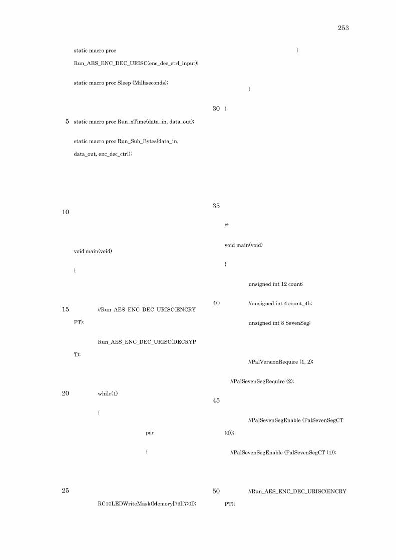
253
static macro proc
Run_AES_ENC_DEC_URISC(enc_dec_ctrl_input);
static macro proc Sleep (Milliseconds);
static macro proc Run_xTime(data_in, data_out); 5
static macro proc Run_Sub_Bytes(data_in,
data_out, enc_dec_ctrl);
10
void main(void)
{
//Run_AES_ENC_DEC_URISC(ENCRY15
PT);
Run_AES_ENC_DEC_URISC(DECRYP
T);
while(1) 20
{
par
{
25
RC10LEDWriteMask(Memory[79][7:0]);
}
}
} 30
35
/*
void main(void)
{
unsigned int 12 count;
//unsigned int 4 count_4b; 40
unsigned int 8 SevenSeg;
//PalVersionRequire (1, 2);
//PalSevenSegRequire (2);
45
//PalSevenSegEnable (PalSevenSegCT
(0));
//PalSevenSegEnable (PalSevenSegCT (1));
//Run_AES_ENC_DEC_URISC(ENCRY50
PT);

254
Run_AES_ENC_DEC_URISC(DECRYP
T);
while(1) 5
{
for(count=64; count<=79;
count++) //aes cipher data (ENC_DEC)
//for(count=16; count<=31;
count++) //aes cipher data 10
//for(count=32; count<=47;
count++) //aes cipher data
{
par 15
{
SevenSeg =
Memory[count][7:0];
RC10SevenSeg0WriteDigit(SevenSeg[7:20
4],0);
RC10SevenSeg1WriteDigit(SevenSeg[3:
0],0);
25
//PalSevenSegWriteDigit(PalSevenSegC
T(0),SevenSeg[7:4],0);
//PalSevenSegWriteDigit(PalSevenSegC
T(1),SevenSeg[3:0],0); 30
RC10LEDWriteMask(count[7:0]);
}
Sleep(1000);
} 35
}
40
// while(1)
// {
45
//
RC10LEDWriteMask(Memory[272][7:0]);
//
Sleep(1000);
50
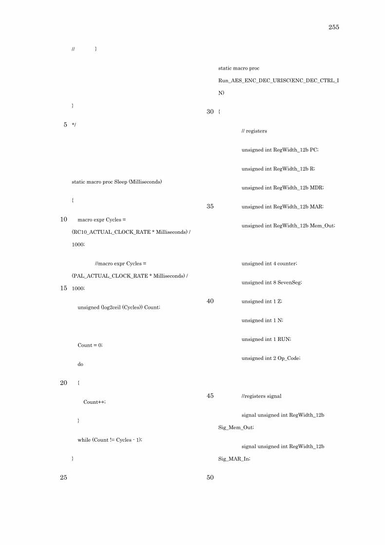
255
// }
}
*/ 5
static macro proc Sleep (Milliseconds)
{
macro expr Cycles = 10
(RC10_ACTUAL_CLOCK_RATE * Milliseconds) /
1000;
//macro expr Cycles =
(PAL_ACTUAL_CLOCK_RATE * Milliseconds) /
1000; 15
unsigned (log2ceil (Cycles)) Count;
Count = 0;
do
{ 20
Count++;
}
while (Count != Cycles - 1);
}
25
static macro proc
Run_AES_ENC_DEC_URISC(ENC_DEC_CTRL_I
N)
{ 30
// registers
unsigned int RegWidth_12b PC;
unsigned int RegWidth_12b R;
unsigned int RegWidth_12b MDR;
unsigned int RegWidth_12b MAR; 35
unsigned int RegWidth_12b Mem_Out;
unsigned int 4 counter;
unsigned int 8 SevenSeg;
unsigned int 1 Z; 40
unsigned int 1 N;
unsigned int 1 RUN;
unsigned int 2 Op_Code;
//registers signal 45
signal unsigned int RegWidth_12b
Sig_Mem_Out;
signal unsigned int RegWidth_12b
Sig_MAR_In;
50
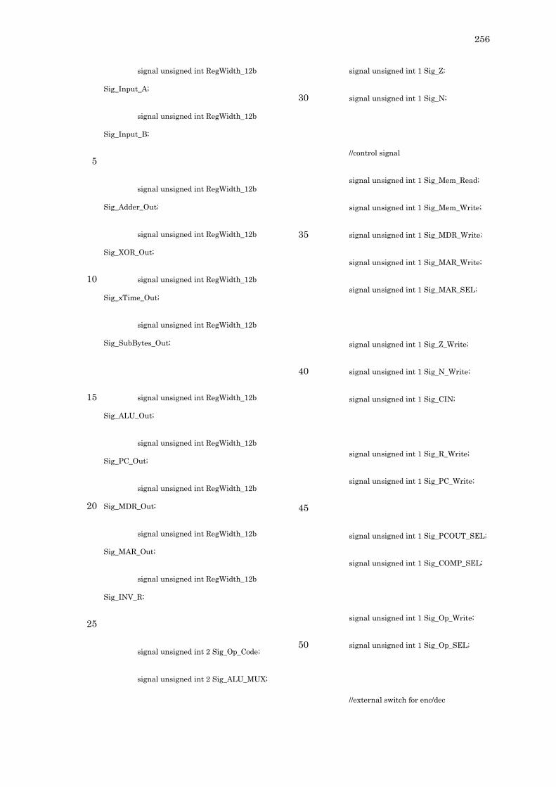
256
signal unsigned int RegWidth_12b
Sig_Input_A;
signal unsigned int RegWidth_12b
Sig_Input_B;
5
signal unsigned int RegWidth_12b
Sig_Adder_Out;
signal unsigned int RegWidth_12b
Sig_XOR_Out;
signal unsigned int RegWidth_12b 10
Sig_xTime_Out;
signal unsigned int RegWidth_12b
Sig_SubBytes_Out;
signal unsigned int RegWidth_12b 15
Sig_ALU_Out;
signal unsigned int RegWidth_12b
Sig_PC_Out;
signal unsigned int RegWidth_12b
Sig_MDR_Out; 20
signal unsigned int RegWidth_12b
Sig_MAR_Out;
signal unsigned int RegWidth_12b
Sig_INV_R;
25
signal unsigned int 2 Sig_Op_Code;
signal unsigned int 2 Sig_ALU_MUX;
signal unsigned int 1 Sig_Z;
signal unsigned int 1 Sig_N; 30
//control signal
signal unsigned int 1 Sig_Mem_Read;
signal unsigned int 1 Sig_Mem_Write;
signal unsigned int 1 Sig_MDR_Write; 35
signal unsigned int 1 Sig_MAR_Write;
signal unsigned int 1 Sig_MAR_SEL;
signal unsigned int 1 Sig_Z_Write;
signal unsigned int 1 Sig_N_Write; 40
signal unsigned int 1 Sig_CIN;
signal unsigned int 1 Sig_R_Write;
signal unsigned int 1 Sig_PC_Write;
45
signal unsigned int 1 Sig_PCOUT_SEL;
signal unsigned int 1 Sig_COMP_SEL;
signal unsigned int 1 Sig_Op_Write;
signal unsigned int 1 Sig_Op_SEL; 50
//external switch for enc/dec
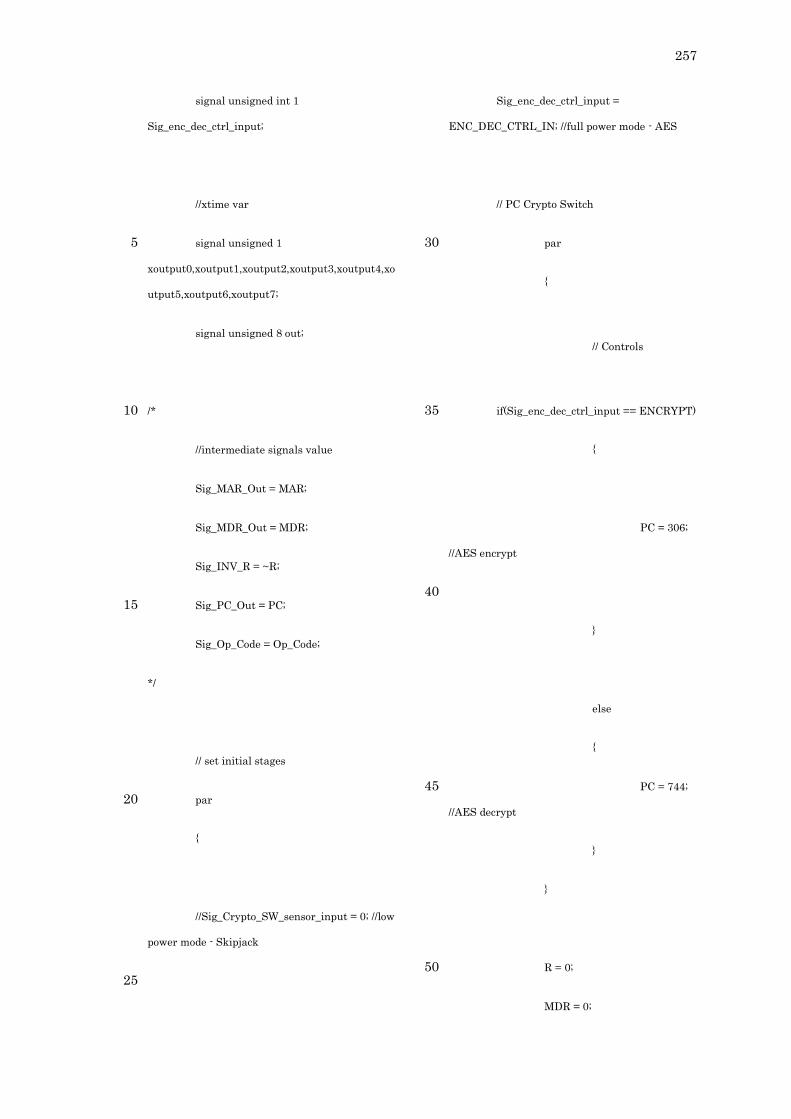
257
signal unsigned int 1
Sig_enc_dec_ctrl_input;
//xtime var
signal unsigned 1 5
xoutput0,xoutput1,xoutput2,xoutput3,xoutput4,xo
utput5,xoutput6,xoutput7;
signal unsigned 8 out;
/* 10
//intermediate signals value
Sig_MAR_Out = MAR;
Sig_MDR_Out = MDR;
Sig_INV_R = ~R;
Sig_PC_Out = PC; 15
Sig_Op_Code = Op_Code;
*/
// set initial stages
par 20
{
//Sig_Crypto_SW_sensor_input = 0; //low
power mode - Skipjack
25
Sig_enc_dec_ctrl_input =
ENC_DEC_CTRL_IN; //full power mode - AES
// PC Crypto Switch
par 30
{
// Controls
if(Sig_enc_dec_ctrl_input == ENCRYPT) 35
{
PC = 306;
//AES encrypt
40
}
else
{
PC = 744; 45
//AES decrypt
}
}
R = 0; 50
MDR = 0;
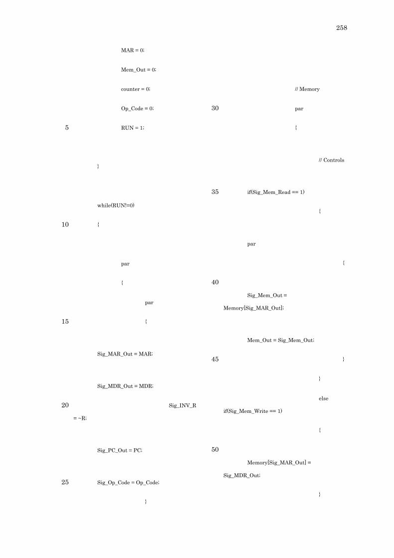
258
MAR = 0;
Mem_Out = 0;
counter = 0;
Op_Code = 0;
RUN = 1; 5
}
while(RUN!=0)
{ 10
par
{
par
{ 15
Sig_MAR_Out = MAR;
Sig_MDR_Out = MDR;
Sig_INV_R 20
= ~R;
Sig_PC_Out = PC;
Sig_Op_Code = Op_Code; 25
}
// Memory
par 30
{
// Controls
if(Sig_Mem_Read == 1) 35
{
par
{
40
Sig_Mem_Out =
Memory[Sig_MAR_Out];
Mem_Out = Sig_Mem_Out;
} 45
}
else
if(Sig_Mem_Write == 1)
{
50
Memory[Sig_MAR_Out] =
Sig_MDR_Out;
}
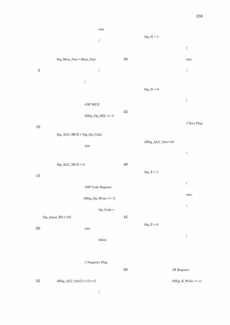
259
else
{
Sig_Mem_Out = Mem_Out;
} 5
}
//OP MUX
if(Sig_Op_SEL == 1)
10
Sig_ALU_MUX = Sig_Op_Code;
else
Sig_ALU_MUX = 0;
15
//OP Code Register
if(Sig_Op_Write == 1)
Op_Code =
Sig_Input_B[11:10];
else 20
delay;
// Negative Flag
if(Sig_ALU_Out[11:11]==1) 25
{
Sig_N = 1;
}
else 30
{
Sig_N = 0;
}
35
// Zero Flag
if(Sig_ALU_Out==0)
{
40
Sig_Z = 1;
}
else
{
45
Sig_Z = 0;
}
//R Register 50
if(Sig_R_Write == 1)

260
R =
Sig_Input_B;
else
delay;
5
//Z Register
if(Sig_Z_Write == 1)
Z = Sig_Z;
else
delay; 10
//N Register
if(Sig_N_Write == 1)
N = Sig_N;
else 15
delay;
//MDR Register
if(Sig_MDR_Write
== 1) 20
MDR =
Sig_ALU_Out;
else
delay;
25
//MAR Register
if(Sig_MAR_Write
== 1)
MAR =
Sig_MAR_In; 30
else
delay;
//MAR SEL MUX
if(Sig_MAR_SEL == 35
1)
Sig_MAR_In = 0[1:0] @
Sig_Mem_Out[9:0];
else 40
Sig_MAR_In = Sig_ALU_Out;
//PC_OUT MUX
if(Sig_PCOUT_SEL 45
== 1)
Sig_Input_B = Sig_Mem_Out;
else
50
Sig_Input_B = Sig_PC_Out;
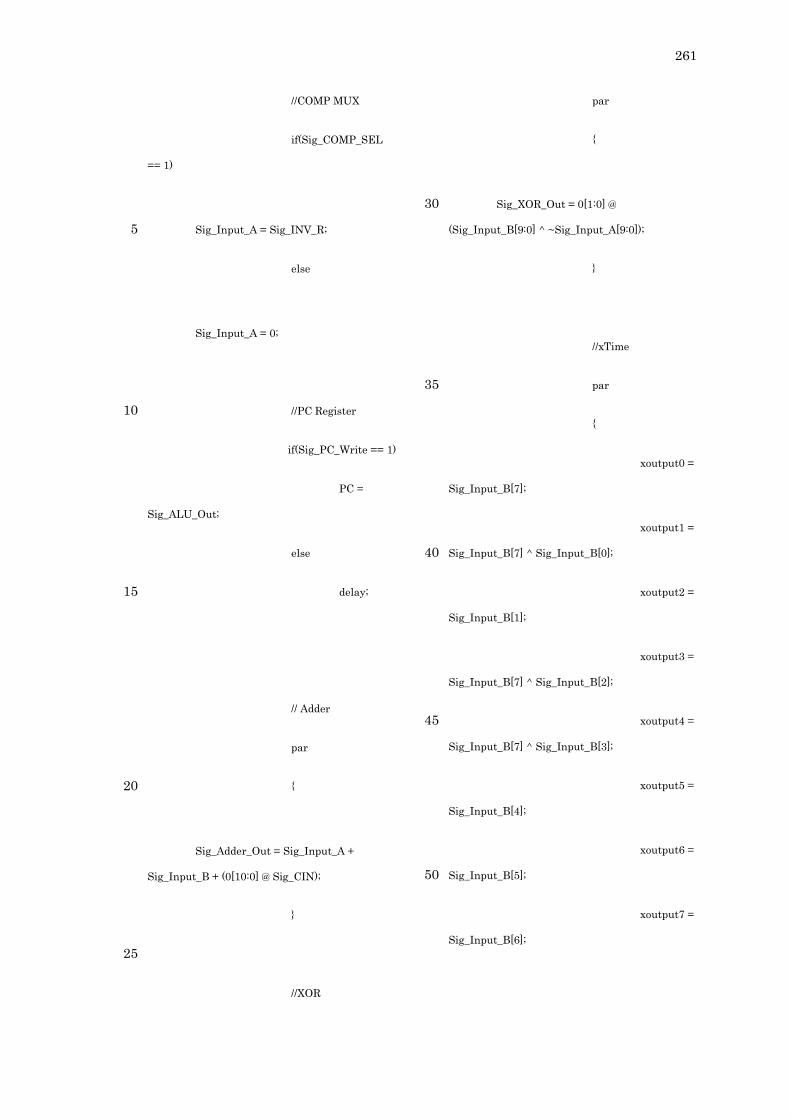
261
//COMP MUX
if(Sig_COMP_SEL
== 1)
Sig_Input_A = Sig_INV_R; 5
else
Sig_Input_A = 0;
//PC Register 10
if(Sig_PC_Write == 1)
PC =
Sig_ALU_Out;
else
delay; 15
// Adder
par
{ 20
Sig_Adder_Out = Sig_Input_A +
Sig_Input_B + (0[10:0] @ Sig_CIN);
}
25
//XOR
par
{
Sig_XOR_Out = 0[1:0] @ 30
(Sig_Input_B[9:0] ^ ~Sig_Input_A[9:0]);
}
//xTime
par 35
{
xoutput0 =
Sig_Input_B[7];
xoutput1 =
Sig_Input_B[7] ^ Sig_Input_B[0]; 40
xoutput2 =
Sig_Input_B[1];
xoutput3 =
Sig_Input_B[7] ^ Sig_Input_B[2];
xoutput4 = 45
Sig_Input_B[7] ^ Sig_Input_B[3];
xoutput5 =
Sig_Input_B[4];
xoutput6 =
Sig_Input_B[5]; 50
xoutput7 =
Sig_Input_B[6];
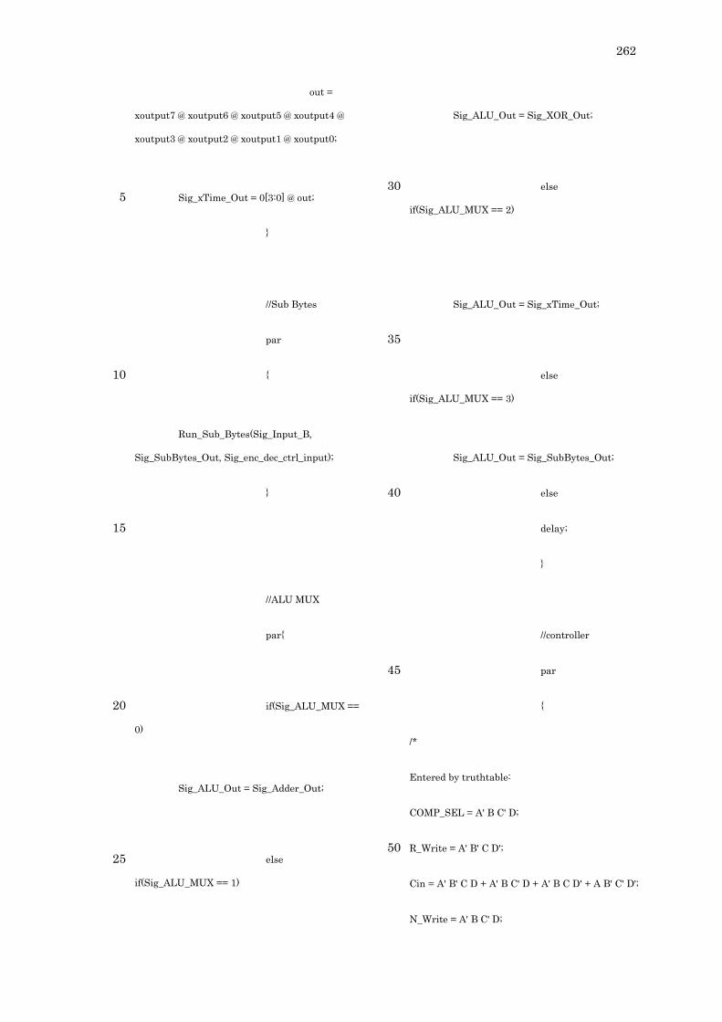
262
out =
xoutput7 @ xoutput6 @ xoutput5 @ xoutput4 @
xoutput3 @ xoutput2 @ xoutput1 @ xoutput0;
Sig_xTime_Out = 0[3:0] @ out; 5
}
//Sub Bytes
par
{ 10
Run_Sub_Bytes(Sig_Input_B,
Sig_SubBytes_Out, Sig_enc_dec_ctrl_input);
}
15
//ALU MUX
par{
if(Sig_ALU_MUX == 20
0)
Sig_ALU_Out = Sig_Adder_Out;
else 25
if(Sig_ALU_MUX == 1)
Sig_ALU_Out = Sig_XOR_Out;
else 30
if(Sig_ALU_MUX == 2)
Sig_ALU_Out = Sig_xTime_Out;
35
else
if(Sig_ALU_MUX == 3)
Sig_ALU_Out = Sig_SubBytes_Out;
else 40
delay;
}
//controller
par 45
{
/*
Entered by truthtable:
COMP_SEL = A' B C' D;
R_Write = A' B' C D'; 50
Cin = A' B' C D + A' B C' D + A' B C D' + A B' C' D';
N_Write = A' B C' D;
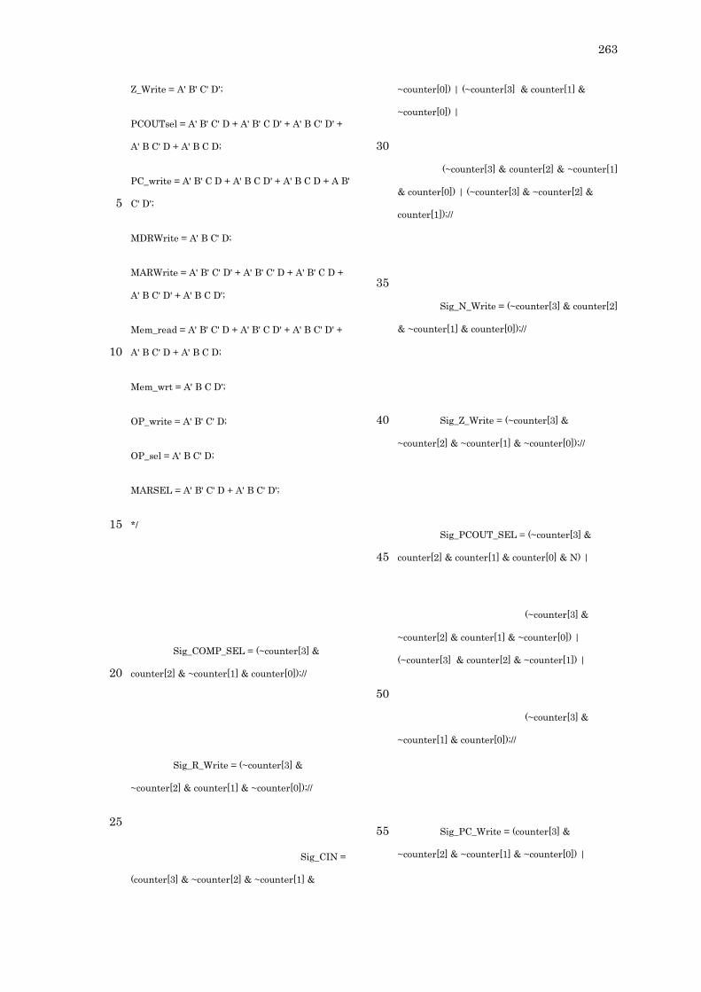
263
Z_Write = A' B' C' D';
PCOUTsel = A' B' C' D + A' B' C D' + A' B C' D' +
A' B C' D + A' B C D;
PC_write = A' B' C D + A' B C D' + A' B C D + A B'
C' D'; 5
MDRWrite = A' B C' D;
MARWrite = A' B' C' D' + A' B' C' D + A' B' C D +
A' B C' D' + A' B C D';
Mem_read = A' B' C' D + A' B' C D' + A' B C' D' +
A' B C' D + A' B C D; 10
Mem_wrt = A' B C D';
OP_write = A' B' C' D;
OP_sel = A' B C' D;
MARSEL = A' B' C' D + A' B C' D';
*/ 15
Sig_COMP_SEL = (~counter[3] &
counter[2] & ~counter[1] & counter[0]);// 20
Sig_R_Write = (~counter[3] &
~counter[2] & counter[1] & ~counter[0]);//
25
Sig_CIN =
(counter[3] & ~counter[2] & ~counter[1] &
~counter[0]) | (~counter[3] & counter[1] &
~counter[0]) |
30
(~counter[3] & counter[2] & ~counter[1]
& counter[0]) | (~counter[3] & ~counter[2] &
counter[1]);//
35
Sig_N_Write = (~counter[3] & counter[2]
& ~counter[1] & counter[0]);//
Sig_Z_Write = (~counter[3] & 40
~counter[2] & ~counter[1] & ~counter[0]);//
Sig_PCOUT_SEL = (~counter[3] &
counter[2] & counter[1] & counter[0] & N) | 45
(~counter[3] &
~counter[2] & counter[1] & ~counter[0]) |
(~counter[3] & counter[2] & ~counter[1]) |
50
(~counter[3] &
~counter[1] & counter[0]);//
Sig_PC_Write = (counter[3] & 55
~counter[2] & ~counter[1] & ~counter[0]) |
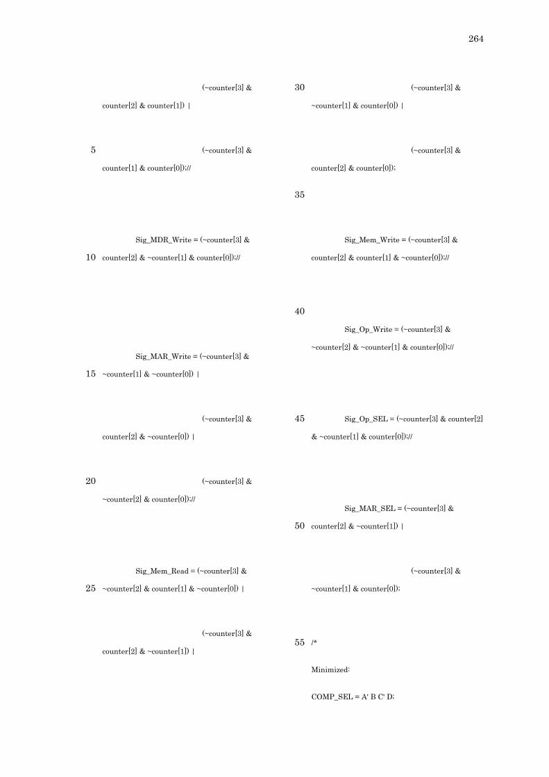
264
(~counter[3] &
counter[2] & counter[1]) |
(~counter[3] & 5
counter[1] & counter[0]);//
Sig_MDR_Write = (~counter[3] &
counter[2] & ~counter[1] & counter[0]);// 10
Sig_MAR_Write = (~counter[3] &
~counter[1] & ~counter[0]) | 15
(~counter[3] &
counter[2] & ~counter[0]) |
(~counter[3] & 20
~counter[2] & counter[0]);//
Sig_Mem_Read = (~counter[3] &
~counter[2] & counter[1] & ~counter[0]) | 25
(~counter[3] &
counter[2] & ~counter[1]) |
(~counter[3] & 30
~counter[1] & counter[0]) |
(~counter[3] &
counter[2] & counter[0]);
35
Sig_Mem_Write = (~counter[3] &
counter[2] & counter[1] & ~counter[0]);//
40
Sig_Op_Write = (~counter[3] &
~counter[2] & ~counter[1] & counter[0]);//
Sig_Op_SEL = (~counter[3] & counter[2] 45
& ~counter[1] & counter[0]);//
Sig_MAR_SEL = (~counter[3] &
counter[2] & ~counter[1]) | 50
(~counter[3] &
~counter[1] & counter[0]);
/* 55
Minimized:
COMP_SEL = A' B C' D;

265
R_Write = A' B' C D';
Cin = A B' C' D' + A' C D' + A' B C' D + A' B' C ;
N_Write = A' B C' D;
Z_Write = A' B' C' D';
PCOUTsel = A' B' C D' + A' B C' + A' C' D + A' B 5
D;
PC_write = A B' C' D' + A' B C + A' C D;
MDRWrite = A' B C' D;
MARWrite = A' C' D' + A' B D' + A' B' D;
Mem_read = A' B' C D' + A' B C' + A' C' D + A' B 10
D;
Mem_wrt = A' B C D';
OP_write = A' B' C' D;
OP_sel = A' B C' D;
MARSEL = A' B C' + A' C' D; 15
*/
if(counter==8)
{ 20
counter = 0;
}
else
{ 25
counter = counter + 1;
}
30
if(PC==4095)
{
RUN = 0;
} 35
else
delay;
}
40
}
}
45
}
50
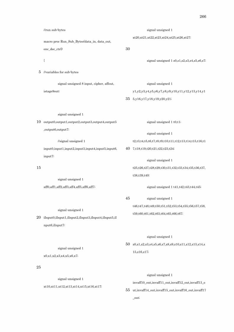
266
//run sub-bytes
macro proc Run_Sub_Bytes(data_in, data_out,
enc_dec_ctrl)
{
//variables for sub-bytes 5
signal unsigned 8 input, cipher, affout,
istage9out;
signal unsigned 1
output0,output1,output2,output3,output4,output510
,output6,output7;
//signal unsigned 1
input0,input1,input2,input3,input4,input5,input6,
input7;
15
signal unsigned 1
aff0,aff1,aff2,aff3,aff4,aff5,aff6,aff7;
signal unsigned 1
iInput0,iInput1,iInput2,iInput3,iInput4,iInput5,iI20
nput6,iInput7;
signal unsigned 1
x0,x1,x2,x3,x4,x5,x6,x7;
25
signal unsigned 1
xt10,xt11,xt12,xt13,xt14,xt15,xt16,xt17;
signal unsigned 1
xt20,xt21,xt22,xt23,xt24,xt25,xt26,xt27;
30
signal unsigned 1 s0,s1,s2,s3,s4,s5,s6,s7;
signal unsigned 1
y1,y2,y3,y4,y5,y6,y7,y8,y9,y10,y11,y12,y13,y14,y1
5,y16,y17,y18,y19,y20,y21; 35
signal unsigned 1 t0,t1;
signal unsigned 1
t2,t3,t4,t5,t6,t7,t8,t9,t10,t11,t12,t13,t14,t15,t16,t1
7,t18,t19,t20,t21,t22,t23,t24; 40
signal unsigned 1
t25,t26,t27,t28,t29,t30,t31,t32,t33,t34,t35,t36,t37,
t38,t39,t40;
signal unsigned 1 t41,t42,t43,t44,t45;
signal unsigned 1 45
t46,t47,t48,t49,t50,t51,t52,t53,t54,t55,t56,t57,t58,
t59,t60,t61,t62,t63,t64,t65,t66,t67;
signal unsigned 1
z0,z1,z2,z3,z4,z5,z6,z7,z8,z9,z10,z11,z12,z13,z14,z50
15,z16,z17;
signal unsigned 1
invaff10_out,invaff11_out,invaff12_out,invaff13_o
ut,invaff14_out,invaff15_out,invaff16_out,invaff1755
_out;
267
signal unsigned 1
invaff20_out,invaff21_out,invaff22_out,invaff23_o
ut,invaff24_out,invaff25_out,invaff26_out,invaff27
_out;
5
signal unsigned 1 u10, u11, u12, u13;
signal unsigned 1 u20, u21, u22, u23;
signal unsigned 1 te10, te11, te20, te21; 10
signal unsigned 1 enc_dec_mux_sw;
par{
15
par{
input = data_in[7:0];
enc_dec_mux_sw = enc_dec_ctrl;
}
20
par
{
xt17 = input[7]; 25
xt16 = input[6];
xt15 = input[5];
xt14 = input[4];
xt13 = input[3];
xt12 = input[2]; 30
xt11 = input[1];
xt10 = input[0];
}
35
//inv affine 1
par
{
u10 = xt11 ^ xt14; 40
u11 = xt13 ^ xt16;
u12 = xt10 ^ xt15;
u13 = xt12 ^ xt17;
invaff17_out = xt16 ^ u10; 45
invaff16_out = xt13 ^ u12;
invaff15_out = xt14 ^ u13;
invaff14_out = xt11 ^ u11;
invaff13_out = xt12 ^ u12;
268
invaff12_out = xt17 ^ u10;
invaff11_out = xt10 ^ u11;
invaff10_out = xt15 ^ u13;
te10 = invaff12_out ^ 1; 5
te11 = invaff10_out ^ 1;
}
10
par{
//encrypt decrypt MUX
if(enc_dec_mux_sw == ENCRYPT)
//ENCRYPT = 1, DECRYPT = 0
{ 15
par{
x0 = xt17;
x1 = xt16;
x2 = xt15;
x3 = xt14; 20
x4 = xt13;
x5 = xt12;
x6 = xt11;
x7 = xt10;
} 25
}
else
{
par{ 30
x0 = invaff17_out;
x1 = invaff16_out;
x2 = invaff15_out;
x3 = invaff14_out;
x4 = invaff13_out; 35
x5 = te10;
x6 = invaff11_out;
x7 = te11;
} 40
}
}
45
269
//top linear transformation
//input: x0,x1,x2,x3...x7
//output: x7,y1,y2,y3...y21
par{
y14 = x3 ^ x5; 5
y13 = x0 ^ x6;
y9 = x0 ^ x3;
y8 = x0 ^ x5;
t0 = x1 ^ x2; 10
y1 = t0 ^ x7;
y4 = y1 ^ x3;
y12 = y13 ^ y14;
y2 = y1 ^ x0; 15
y5 = y1 ^ x6;
y3 = y5 ^ y8;
t1 = x4 ^ y12;
20
y15 = t1 ^ x5;
y20 = t1 ^ x1;
y6 = y15 ^ x7;
y10 = y15 ^ t0; 25
y11 = y20 ^ y9;
y7 = x7 ^ y11;
y17 = y10 ^ y11;
y19 = y10 ^ y8; 30
y16 = t0 ^ y11;
y21 = y13 ^ y16;
y18 = x0 ^ y16;
} 35
//middle non-linear section
//input: x7,y1,y2,y3...y21
//output: z0,z1...z17
40
//t25 -> t40 inversion in GF(2^4)
par{
t2 = y12 & y15;
t3 = y3 & y6;
t4 = t3 ^ t2; 45
t5 = y4 & x7;
t6 = t5 ^ t2;

270
t7 = y13 & y16;
t8 = y5 & y1;
t9 = t8 ^ t7;
t10 = y2 & y7; 5
t11 = t10 ^ t7;
t12 = y9 & y11;
t13 = y14 & y17;
10
t14 = t13 ^ t12;
t15 = y8 & y10;
t16 = t15 ^ t12;
t17 = t4 ^ t14; 15
t18 = t6 ^ t16;
t19 = t9 ^ t14;
t20 = t11 ^ t16;
t21 = t17 ^ y20; 20
t22 = t18 ^ y19;
t23 = t19 ^ y21;
t24 = t20 ^ y18;
25
//inversion in GF(2^4)
t25 = t21 ^ t22;
t26 = t21 & t23; 30
t27 = t24 ^ t26;
t28 = t25 & t27;
t29 = t28 ^ t22;
t30 = t23 ^ t24; 35
t31 = t22 ^ t26;
t32 = t31 & t30;
t33 = t32 ^ t24;
40
t34 = t23 ^ t33;
t35 = t27 ^ t33;
t36 = t24 & t35;
t37 = t36 ^ t34; 45
t38 = t27 ^ t36;
t39 = t29 & t38;

271
t40 = t25 ^ t39;
t41 = t40 ^ t37;
t42 = t29 ^ t33; 5
t43 = t29 ^ t40;
t44 = t33 ^ t37;
t45 = t42 ^ t41;
10
z0 = t44 & y15;
z1 = t37 & y6;
z2 = t33 & x7;
z3 = t43 & y16; 15
z4 = t40 & y1;
z5 = t29 & y7;
z6 = t42 & y11;
z7 = t45 & y17; 20
z8 = t41 & y10;
z9 = t44 & y12;
z10 = t37 & y3;
z11 = t33 & y4; 25
z12 = t43 & y13;
z13 = t40 & y5;
z14 = t29 & y2;
30
z15 = t42 & y9;
z16 = t45 & y14;
z17 = t41 & y8;
}
35
//bottom linear transformation
//input:z0,z1...z17
//output:so,s1...s7
par{
t46 = z15 ^ z16; 40
t47 = z10 ^ z11;
t48 = z5 ^ z13;
t49 = z9 ^ z10;
t50 = z2 ^ z12; 45
t51 = z2 ^ z5;
t52 = z7 ^ z8;
272
t53 = z0 ^ z3;
t54 = z6 ^ z7;
t55 = z16 ^ z17;
t56 = z12 ^ t48; 5
t57 = t50 ^ t53;
t58 = z4 ^ t46;
t59 = z3 ^ t54;
t60 = t46 ^ t57; 10
t61 = z14 ^ t57;
t62 = t52 ^ t58;
t63 = t49 ^ t58;
15
t64 = z4 ^ t59;
t65 = t61 ^ t62;
t66 = z1 ^ t63;
s0 = t59 ^ t63; 20
s6 = ~(t56 ^ t62);
s7 = ~(t48 ^ t60);
t67 = t64 ^ t65;
s3 = t53 ^ t66; 25
s4 = t51 ^ t66;
s5 = t47 ^ t65;
s1 = ~(t64 ^ s3);
s2 = ~(t55 ^ t67); 30
}
//output inverse
par{ 35
xt27 = s0;
xt26 = s1;
xt25 = s2;
xt24 = s3;
xt23 = s4; 40
xt22 = s5;
xt21 = s6;
xt20 = s7;
}
45
//inv affine 2
273
par
{
u20 = xt21 ^ xt24;
u21 = xt23 ^ xt26;
u22 = xt20 ^ xt25; 5
u23 = xt22 ^ xt27;
invaff27_out = xt26 ^ u20;
invaff26_out = xt23 ^ u22;
invaff25_out = xt24 ^ u23; 10
invaff24_out = xt21 ^ u21;
invaff23_out = xt22 ^ u22;
invaff22_out = xt27 ^ u20;
invaff21_out = xt20 ^ u21;
invaff20_out = xt25 ^ u23; 15
te20 = invaff22_out ^ 1;
te21 = invaff20_out ^ 1;
}
20
par{
//encrypt decrypt MUX
if(enc_dec_mux_sw == ENCRYPT) 25
//ENCRYPT = 1, DECRYPT = 0
{
par{
output7 = xt27;
output6 = xt26; 30
output5 = xt25;
output4 = xt24;
output3 = xt23;
output2 = xt22;
output1 = xt21; 35
output0 = xt20;
}
}
else 40
{
par{
output7 = invaff27_out;
output6 = invaff26_out;
output5 = invaff25_out; 45
output4 = invaff24_out;
output3 = invaff23_out;
output2 = te20;
274
output1 = invaff21_out;
output0 = te21;
}
5
}
}
10
par{
cipher = output7 @ output6 @ output5 @
output4 @ output3 @ output2 @ output1 @ output0;
data_out = 0[3:0] @ cipher;
} 15
}
}
20

275
APPENDIX II: PHOTOGRAPHS
Celoxica RC10 Board
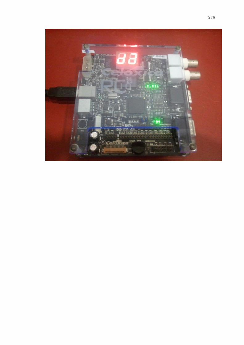
276
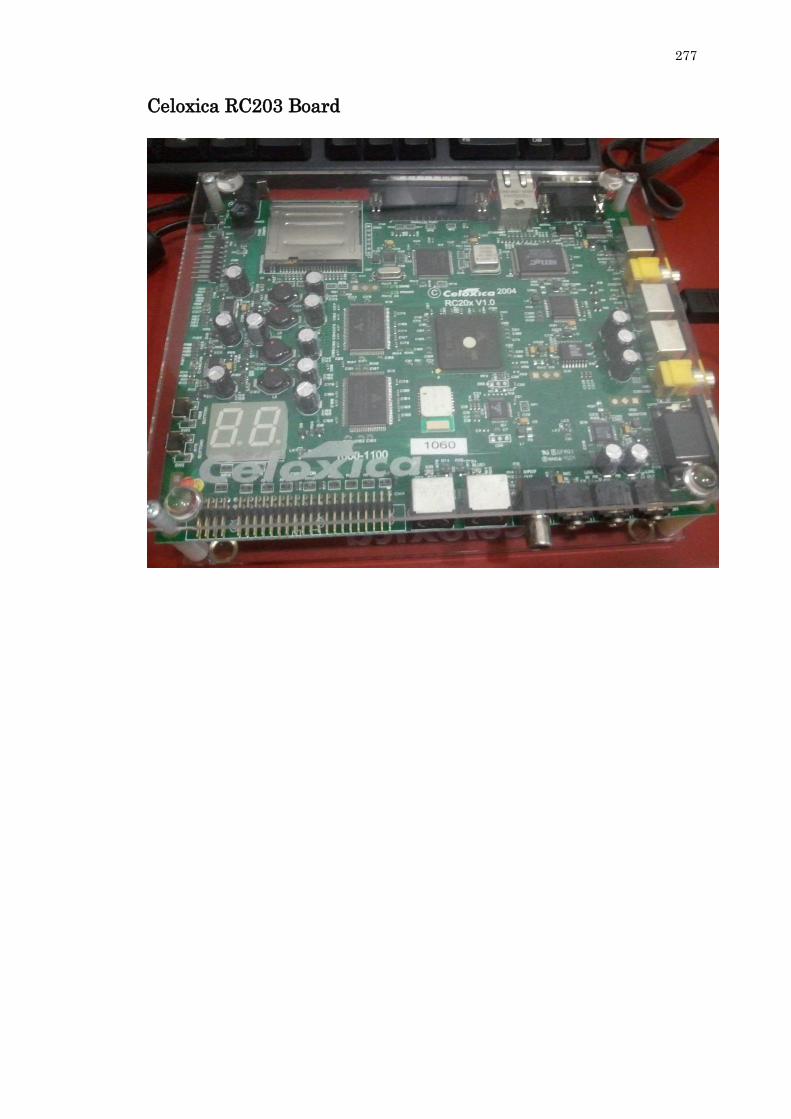
277
Celoxica RC203 Board