logicore ip system cache v1the cache memory provides the actual cache functionality in the system...
TRANSCRIPT
LogiCORE IP System Cache v1.01c
Product Guide
PG031 December 18, 2012
System Cache v1.01c www.xilinx.com 2PG031 December 18, 2012
Table of Contents
SECTION I: SUMMARY
IP Facts
Chapter 1: OverviewFeature Summary. . . . . . . . . . . . . . . . . . . . . . . . . . . . . . . . . . . . . . . . . . . . . . . . . . . . . . . . . . . . . . . . . . 6Applications . . . . . . . . . . . . . . . . . . . . . . . . . . . . . . . . . . . . . . . . . . . . . . . . . . . . . . . . . . . . . . . . . . . . . 11Unsupported Features. . . . . . . . . . . . . . . . . . . . . . . . . . . . . . . . . . . . . . . . . . . . . . . . . . . . . . . . . . . . . 13Licensing and Ordering Information . . . . . . . . . . . . . . . . . . . . . . . . . . . . . . . . . . . . . . . . . . . . . . . . . . 14
Chapter 2: Product SpecificationStandards . . . . . . . . . . . . . . . . . . . . . . . . . . . . . . . . . . . . . . . . . . . . . . . . . . . . . . . . . . . . . . . . . . . . . . . 15Performance. . . . . . . . . . . . . . . . . . . . . . . . . . . . . . . . . . . . . . . . . . . . . . . . . . . . . . . . . . . . . . . . . . . . . 15Resource Utilization. . . . . . . . . . . . . . . . . . . . . . . . . . . . . . . . . . . . . . . . . . . . . . . . . . . . . . . . . . . . . . . 17Port Descriptions . . . . . . . . . . . . . . . . . . . . . . . . . . . . . . . . . . . . . . . . . . . . . . . . . . . . . . . . . . . . . . . . . 19Register Space . . . . . . . . . . . . . . . . . . . . . . . . . . . . . . . . . . . . . . . . . . . . . . . . . . . . . . . . . . . . . . . . . . . 20
Chapter 3: Designing with the CoreGeneral Design Guidelines . . . . . . . . . . . . . . . . . . . . . . . . . . . . . . . . . . . . . . . . . . . . . . . . . . . . . . . . . 28Clocking. . . . . . . . . . . . . . . . . . . . . . . . . . . . . . . . . . . . . . . . . . . . . . . . . . . . . . . . . . . . . . . . . . . . . . . . . 29Resets . . . . . . . . . . . . . . . . . . . . . . . . . . . . . . . . . . . . . . . . . . . . . . . . . . . . . . . . . . . . . . . . . . . . . . . . . . 30Protocol Description . . . . . . . . . . . . . . . . . . . . . . . . . . . . . . . . . . . . . . . . . . . . . . . . . . . . . . . . . . . . . . 30
SECTION II: VIVADO DESIGN SUITE
Chapter 4: Customizing and Generating the CoreGUI . . . . . . . . . . . . . . . . . . . . . . . . . . . . . . . . . . . . . . . . . . . . . . . . . . . . . . . . . . . . . . . . . . . . . . . . . . . . 32Parameter Values. . . . . . . . . . . . . . . . . . . . . . . . . . . . . . . . . . . . . . . . . . . . . . . . . . . . . . . . . . . . . . . . . 34
Chapter 5: Constraining the CoreRequired Constraints . . . . . . . . . . . . . . . . . . . . . . . . . . . . . . . . . . . . . . . . . . . . . . . . . . . . . . . . . . . . . . 36
System Cache v1.01c www.xilinx.com 3PG031 December 18, 2012
Device, Package, and Speed Grade Selections. . . . . . . . . . . . . . . . . . . . . . . . . . . . . . . . . . . . . . . . . . 36Clock Frequencies . . . . . . . . . . . . . . . . . . . . . . . . . . . . . . . . . . . . . . . . . . . . . . . . . . . . . . . . . . . . . . . . 36Clock Management . . . . . . . . . . . . . . . . . . . . . . . . . . . . . . . . . . . . . . . . . . . . . . . . . . . . . . . . . . . . . . . 36Clock Placement. . . . . . . . . . . . . . . . . . . . . . . . . . . . . . . . . . . . . . . . . . . . . . . . . . . . . . . . . . . . . . . . . . 36Banking . . . . . . . . . . . . . . . . . . . . . . . . . . . . . . . . . . . . . . . . . . . . . . . . . . . . . . . . . . . . . . . . . . . . . . . . . 36Transceiver Placement . . . . . . . . . . . . . . . . . . . . . . . . . . . . . . . . . . . . . . . . . . . . . . . . . . . . . . . . . . . . 37I/O Standard and Placement. . . . . . . . . . . . . . . . . . . . . . . . . . . . . . . . . . . . . . . . . . . . . . . . . . . . . . . . 37
SECTION III: ISE DESIGN SUITE
Chapter 6: Customizing and Generating the CoreGUI . . . . . . . . . . . . . . . . . . . . . . . . . . . . . . . . . . . . . . . . . . . . . . . . . . . . . . . . . . . . . . . . . . . . . . . . . . . . 39Parameter Values. . . . . . . . . . . . . . . . . . . . . . . . . . . . . . . . . . . . . . . . . . . . . . . . . . . . . . . . . . . . . . . . . 41
Chapter 7: Constraining the Core
SECTION IV: APPENDICES
Appendix A: MigratingPort Changes . . . . . . . . . . . . . . . . . . . . . . . . . . . . . . . . . . . . . . . . . . . . . . . . . . . . . . . . . . . . . . . . . . . . 44Functionality Changes . . . . . . . . . . . . . . . . . . . . . . . . . . . . . . . . . . . . . . . . . . . . . . . . . . . . . . . . . . . . . 44
Appendix B: DebuggingFinding Help on Xilinx.com . . . . . . . . . . . . . . . . . . . . . . . . . . . . . . . . . . . . . . . . . . . . . . . . . . . . . . . . . 45Debug Tools . . . . . . . . . . . . . . . . . . . . . . . . . . . . . . . . . . . . . . . . . . . . . . . . . . . . . . . . . . . . . . . . . . . . . 46Simulation Debug. . . . . . . . . . . . . . . . . . . . . . . . . . . . . . . . . . . . . . . . . . . . . . . . . . . . . . . . . . . . . . . . . 47Hardware Debug . . . . . . . . . . . . . . . . . . . . . . . . . . . . . . . . . . . . . . . . . . . . . . . . . . . . . . . . . . . . . . . . . 47Interface Debug . . . . . . . . . . . . . . . . . . . . . . . . . . . . . . . . . . . . . . . . . . . . . . . . . . . . . . . . . . . . . . . . . . 48
Appendix C: Application Software DevelopmentDevice Drivers . . . . . . . . . . . . . . . . . . . . . . . . . . . . . . . . . . . . . . . . . . . . . . . . . . . . . . . . . . . . . . . . . . . 50
Appendix D: Additional ResourcesXilinx Resources . . . . . . . . . . . . . . . . . . . . . . . . . . . . . . . . . . . . . . . . . . . . . . . . . . . . . . . . . . . . . . . . . . 51References . . . . . . . . . . . . . . . . . . . . . . . . . . . . . . . . . . . . . . . . . . . . . . . . . . . . . . . . . . . . . . . . . . . . . . 51Technical Support . . . . . . . . . . . . . . . . . . . . . . . . . . . . . . . . . . . . . . . . . . . . . . . . . . . . . . . . . . . . . . . . 52Revision History . . . . . . . . . . . . . . . . . . . . . . . . . . . . . . . . . . . . . . . . . . . . . . . . . . . . . . . . . . . . . . . . . . 52Notice of Disclaimer. . . . . . . . . . . . . . . . . . . . . . . . . . . . . . . . . . . . . . . . . . . . . . . . . . . . . . . . . . . . . . . 52Automotive Applications Disclaimer . . . . . . . . . . . . . . . . . . . . . . . . . . . . . . . . . . . . . . . . . . . . . . . . . 53
System Cache v1.01c www.xilinx.com 4PG031 December 18, 2012
SECTION I: SUMMARY
IP Facts
Overview
Product Specification
Designing with the Core
System Cache v1.01c www.xilinx.com 5PG031 December 18, 2012 Product Specification
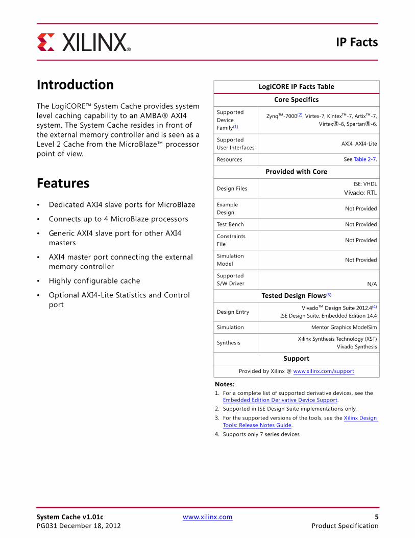
IntroductionThe LogiCORE™ System Cache provides system level caching capability to an AMBA® AXI4 system. The System Cache resides in front of the external memory controller and is seen as a Level 2 Cache from the MicroBlaze™ processor point of view.
Features• Dedicated AXI4 slave ports for MicroBlaze
• Connects up to 4 MicroBlaze processors
• Generic AXI4 slave port for other AXI4 masters
• AXI4 master port connecting the external memory controller
• Highly configurable cache
• Optional AXI4-Lite Statistics and Control port
IP Facts
LogiCORE IP Facts Table
Core Specifics
Supported Device Family(1)
Zynq™-7000(2), Virtex-7, Kintex™-7, Artix™-7,Virtex®-6, Spartan®-6,
Supported User Interfaces
AXI4, AXI4-Lite
Resources See Table 2-7.
Provided with Core
Design FilesISE: VHDL
Vivado: RTL
Example Design
Not Provided
Test Bench Not Provided
Constraints File
Not Provided
Simulation Model
Not Provided
Supported S/W Driver N/A
Tested Design Flows(3)
Design Entry Vivado™ Design Suite 2012.4(4)
ISE Design Suite, Embedded Edition 14.4
Simulation Mentor Graphics ModelSim
Synthesis Xilinx Synthesis Technology (XST)
Vivado Synthesis
Support
Provided by Xilinx @ www.xilinx.com/support
Notes: 1. For a complete list of supported derivative devices, see the
Embedded Edition Derivative Device Support.
2. Supported in ISE Design Suite implementations only.
3. For the supported versions of the tools, see the Xilinx Design Tools: Release Notes Guide.
4. Supports only 7 series devices .
System Cache v1.01c www.xilinx.com 6PG031 December 18, 2012
Chapter 1
Overview
Feature SummaryThe System Cache can be added to an AXI system to improve overall system computing performance, regarding accesses to external memory. The System Cache is typically used in a MicroBlaze™ system implementing a Level 2 Cache with up to four MicroBlaze processors. The generic AXI4 interface provides access to the caching capability for all other AXI4 masters in the system.
PerformanceThe effect the System Cache has on performance is very system and application dependent. Application and system characteristics where performance improvements can be expected are:
• Applications with repeated access of data occupying a certain address range, for example, when external memory is used to buffer data during computations. In particular, performance improvements are achieved when the data set exceeds the capacity of the MicroBlaze internal data cache.
• Systems with small MicroBlaze caches, for example, when the MicroBlaze implementation is tuned to achieve as high frequency as possible. In this case, the increased system frequency contributes to the performance improvements, and the System Cache alleviates the performance loss incurred by the reduced size of the MicroBlaze internal caches.
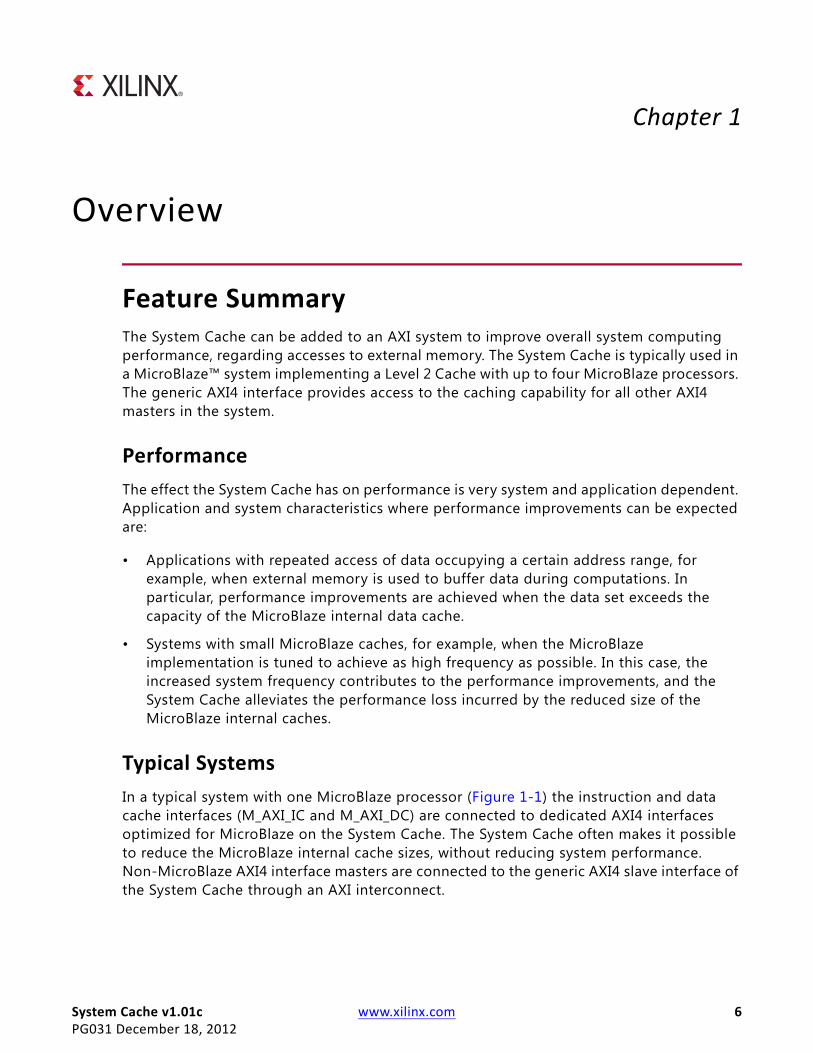
Typical SystemsIn a typical system with one MicroBlaze processor (Figure 1-1) the instruction and data cache interfaces (M_AXI_IC and M_AXI_DC) are connected to dedicated AXI4 interfaces optimized for MicroBlaze on the System Cache. The System Cache often makes it possible to reduce the MicroBlaze internal cache sizes, without reducing system performance. Non-MicroBlaze AXI4 interface masters are connected to the generic AXI4 slave interface of the System Cache through an AXI interconnect.
System Cache v1.01c www.xilinx.com 7PG031 December 18, 2012
Chapter 1: Overview
The System Cache can also be used in a system without any MicroBlaze processor, as shown in Figure 1-2.
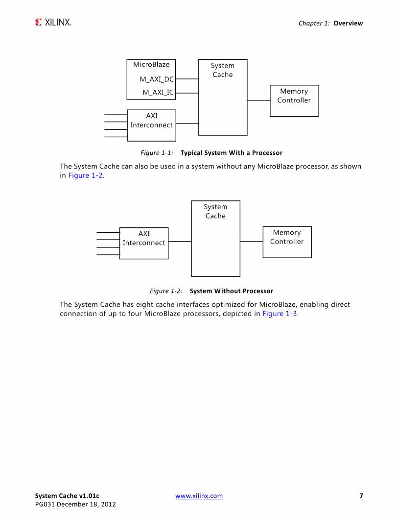
The System Cache has eight cache interfaces optimized for MicroBlaze, enabling direct connection of up to four MicroBlaze processors, depicted in Figure 1-3.
X-Ref Target - Figure 1-1
Figure 1-1: Typical System With a Processor
X-Ref Target - Figure 1-2
Figure 1-2: System Without Processor
Memory Controller
System Cache
AXI Interconnect
MicroBlaze
M_AXI_DC
M_AXI_IC
Memory Controller
System Cache
AXI Interconnect
System Cache v1.01c www.xilinx.com 8PG031 December 18, 2012
Chapter 1: Overview
MicroBlaze Optimized AXI4 Slave InterfaceThe System Cache has eight AXI4 interfaces optimized for access by the cache interfaces on MicroBlaze. Because MicroBlaze has one AXI4 interface for the instruction cache and one for the data cache, systems with up to four MicroBlaze processors are supported.
By using a 1:1 AXI interconnect to directly connect MicroBlaze and the System Cache, access latency for MicroBlaze cache misses is reduced, which improves performance. The optimization to only handle the types of AXI4 accesses issued by MicroBlaze simplif ies the implementation, saving area resources as well as improving performance. The data widths of the MicroBlaze optimized interfaces are parameterized to match the data widths of the connected MicroBlaze processors. With wide interfaces the MicroBlaze cache line length normally determines the data width.
The Optimized AXI4 slave interfaces are compliant to a subset of the AXI4 interface specification. The interface includes the following features and exceptions.
• Support for 32-, 128-, 256-, and 512-bit data widths
• Support for some AXI4 burst types and sizes
° No support for FIXED bursts
° WRAP bursts corresponding to the MicroBlaze cache line length, that is, either 4 beats or 8 beats
X-Ref Target - Figure 1-3
Figure 1-3: Typical System With Multiple MicroBlaze Processors
Memory Controller
System Cache
AXI Interconnect
MicroBlaze
MicroBlaze
M_AXI_DC
M_AXI_IC
M_AXI_DC
M_AXI_IC
System Cache v1.01c www.xilinx.com 9PG031 December 18, 2012
Chapter 1: Overview
° Single beat INCR burst, or either 4 beats or 8 beats corresponding to the MicroBlaze cache line length
° Exclusive accesses are treated as a normal accesses, never returning EXOKAY
° Only support for native transaction size, that is, same as data width for the port
• Support for burst sizes that are less than the data width, with either 32-, 128-, 256-, or 512-bits
• AXI user signals are not necessary or supported
• All transactions executed in order regardless of thread ID value. No read reordering or write reordering is implemented.
Generic AXI4 Slave InterfaceTo handle several AXI4 masters in a system, an AXI interconnect is used to share the single generic AXI4 slave interface on the System Cache. The generic AXI4 interface has a configurable data width to eff iciently match the connected AXI4 masters. This ensures that both the system area and the AXI4 access latency are reduced.
The Generic AXI4 slave interface is compliant to the full AXI4 interface specif ication. The interface includes the following features and exceptions.
• Support for 32-, 64-, 128-, 256-, and 512-bit data widths
• Support for all AXI4 burst types and sizes
° FIXED bursts are handled as INCR type burst operations (no QUEUE burst capability)
° 16 beats for WRAP bursts
° 16 beats for FIXED bursts (treated as INCR burst type)
° 256 beats for INCR burst
° Exclusive accesses are treated as a normal accesses, never returning EXOKAY
• Support for burst sizes that are less than the data width, narrow bursts
• AXI user signals are not necessary or supported
• All transactions executed in order regardless of thread ID value. No read reordering or write reordering is implemented.
System Cache v1.01c www.xilinx.com 10PG031 December 18, 2012
Chapter 1: Overview
Memory Controller AXI4 Master InterfaceThe AXI4 master interface is used to connect the external memory controller. The data width of the interface can be parameterized to match the data width of the AXI4 slave interface on the memory controller. For best performance and resource usage, the parameters on the interface and the Memory Controller should match.
The Memory Controller AXI4 master interface is compliant to the AXI4 interface specification. The interface includes the following features.
• Support for 32-, 64-, 128-, 256-, and 512-bit data widths
• Generates the following AXI4 burst types and sizes
° 2 - 16 beats for WRAP bursts
° 1 - 16 beats for INCR burst
• AXI user signals are not provided
• A single thread ID value is generated
Cache MemoryThe Cache memory provides the actual cache functionality in the System Cache. The cache is configurable in terms of size and associativity.
The cache size can be configured with the parameter C_CACHE_SIZE according to Table 4-1. The selected size is a trade-off between performance and resource usage, in particular the number of block RAMs.
The associativity can be configured with the parameter C_NUM_SETS according to Table 4-1. Increased associativity generally provides better hit rate, which gives better performance but requires more area resources.
The correspondence between selected parameters and used block RAMs is listed in Table 2-7.
Statistics and ControlThe optional Statistics and Control block can be used to collect cache statistics such as cache hit rate and access latency. The statistics is primarily intended for internal Xilinx use, but can also be utilized to tailor the configuration of the System Cache to meet the needs of a specif ic application.
System Cache v1.01c www.xilinx.com 11PG031 December 18, 2012
Chapter 1: Overview
The following types of statistics are collected:
• Port statistics for each slave interface
° Total Read and Write transaction counts
° Port queue usage for the six transaction queues associated with each port
° Cache hit rates for read and write
° Read and Write transaction latency
• Arbitration statistics
• Functional unit statistics
° Stall cycles
° Internal queue usage
• Port statistics for the master interface
° Read and write latency
For details on the registers used to read statistics and control how statistics is gathered, see Chapter 2, Register Space.
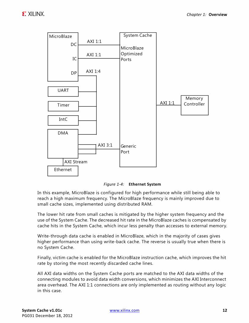
ApplicationsAn example of an Ethernet communication system is given in Figure 1-4. The system consists of a MicroBlaze processor connected point-to-point to two optimized ports of the System Cache. A DMA controller is connected to the generic port of the System Cache through a 3:1 AXI interconnect, because the DMA controller has three AXI master ports. The DMA in turn is connected to the Ethernet IP by AXI4-Stream links. Standard peripheral functions like UART, timer, interrupt controller as well as the DMA controller control port are connected to the MicroBlaze peripheral data port (M_AXI_DP) for register configuration and control.
With this partitioning the bandwidth critical interfaces are connected directly to the System Cache and kept completely separated from the AXI4-Lite based configuration and control connections.
This system is used as an example throughout this guide.
System Cache v1.01c www.xilinx.com 12PG031 December 18, 2012
Chapter 1: Overview
In this example, MicroBlaze is configured for high performance while still being able to reach a high maximum frequency. The MicroBlaze frequency is mainly improved due to small cache sizes, implemented using distributed RAM.
The lower hit rate from small caches is mitigated by the higher system frequency and the use of the System Cache. The decreased hit rate in the MicroBlaze caches is compensated by cache hits in the System Cache, which incur less penalty than accesses to external memory.
Write-through data cache is enabled in MicroBlaze, which in the majority of cases gives higher performance than using write-back cache. The reverse is usually true when there is no System Cache.
Finally, victim cache is enabled for the MicroBlaze instruction cache, which improves the hit rate by storing the most recently discarded cache lines.
All AXI data widths on the System Cache ports are matched to the AXI data widths of the connecting modules to avoid data width conversions, which minimizes the AXI Interconnect area overhead. The AXI 1:1 connections are only implemented as routing without any logic in this case.
X-Ref Target - Figure 1-4
Figure 1-4: Ethernet System
Memory Controller
System Cache
DMA
MicroBlaze
DC
IC
DP
UART
Timer
IntC
Ethernet
AXI 1:1
AXI 1:1
AXI 1:1
AXI 3:1
AXI 1:4
AXI Stream
MicroBlaze Optimized Ports
Generic Port
System Cache v1.01c www.xilinx.com 13PG031 December 18, 2012
Chapter 1: Overview
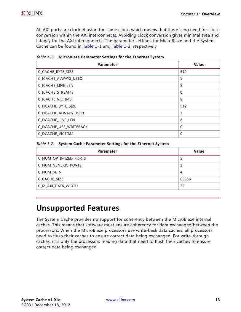
All AXI ports are clocked using the same clock, which means that there is no need for clock conversion within the AXI interconnects. Avoiding clock conversion gives minimal area and latency for the AXI interconnects. The parameter settings for MicroBlaze and the System Cache can be found in Table 1-1 and Table 1-2, respectively
Unsupported FeaturesThe System Cache provides no support for coherency between the MicroBlaze internal caches. This means that software must ensure coherency for data exchanged between the processors. When the MicroBlaze processors use write-back data caches, all processors need to flush their caches to ensure correct data being exchanged. For write-through caches, it is only the processors reading data that need to flush their caches to ensure correct data being exchanged.
Table 1-1: MicroBlaze Parameter Settings for the Ethernet System
Parameter Value
C_CACHE_BYTE_SIZE 512
C_ICACHE_ALWAYS_USED 1
C_ICACHE_LINE_LEN 8
C_ICACHE_STREAMS 0
C_ICACHE_VICTIMS 8
C_DCACHE_BYTE_SIZE 512
C_DCACHE_ALWAYS_USED 1
C_DCACHE_LINE_LEN 8
C_DCACHE_USE_WRITEBACK 0
C_DCACHE_VICTIMS 0
Table 1-2: System Cache Parameter Settings for the Ethernet System
Parameter Value
C_NUM_OPTIMIZED_PORTS 2
C_NUM_GENERIC_PORTS 1
C_NUM_SETS 4
C_CACHE_SIZE 65536
C_M_AXI_DATA_WIDTH 32
System Cache v1.01c www.xilinx.com 14PG031 December 18, 2012
Chapter 1: Overview
Licensing and Ordering InformationThis Xilinx LogiCORE™ IP module is provided at no additional cost with the Xilinx Vivado™ Design Suite and ISE® Design Suite Embedded Edition tools under the terms of the Xilinx End User License.
For information on pricing and availability of other Xilinx LogiCORE IP modules and tools, contact your local Xilinx sales representative.
System Cache v1.01c www.xilinx.com 15PG031 December 18, 2012
Chapter 2
Product Specification
StandardsThe System Core adheres to the AMBA® AXI4 Interface standard [Ref 1] and [Ref 2].
PerformanceThe perceived performance is dependent on many factors such as frequency, latency and throughput. Which factor has the dominating effect is application-specific. There is also a correlation between the performance factors, for example, achieving high frequency can add latency and wide datapaths for throughput can affect frequency.
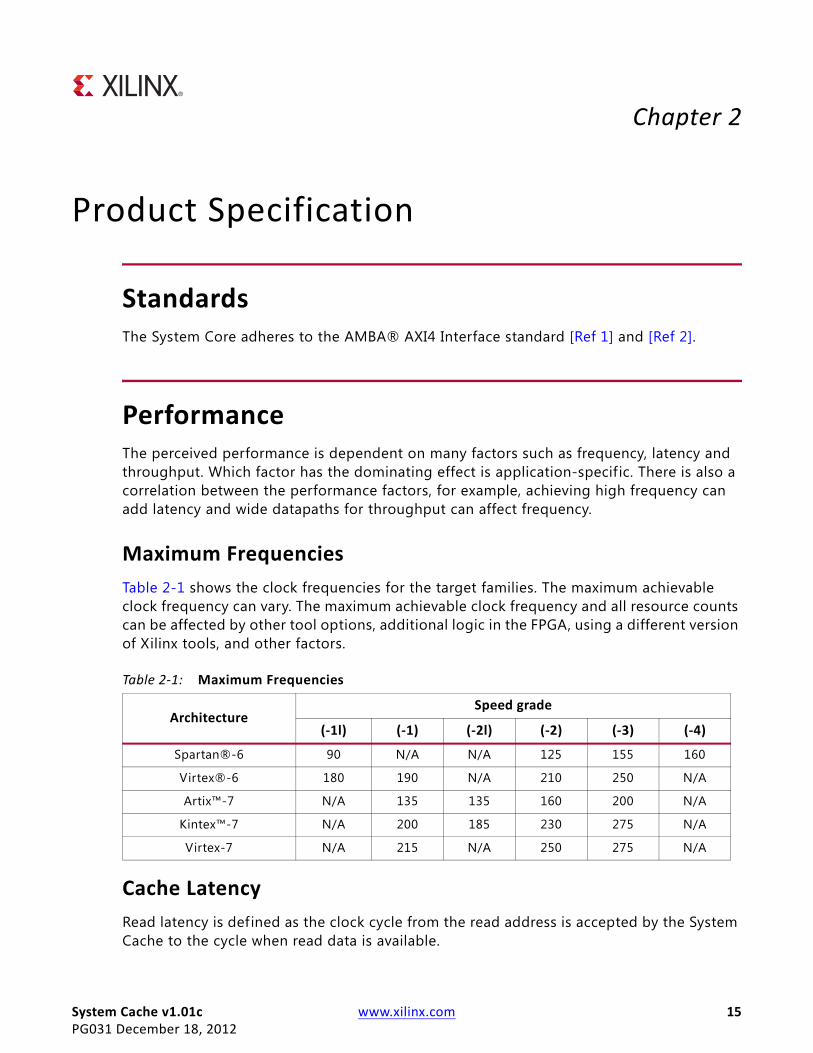
Maximum FrequenciesTable 2-1 shows the clock frequencies for the target families. The maximum achievable clock frequency can vary. The maximum achievable clock frequency and all resource counts can be affected by other tool options, additional logic in the FPGA, using a different version of Xilinx tools, and other factors.
Cache LatencyRead latency is defined as the clock cycle from the read address is accepted by the System Cache to the cycle when read data is available.
Table 2-1: Maximum Frequencies
ArchitectureSpeed grade
(-1l) (-1) (-2l) (-2) (-3) (-4)
Spartan®-6 90 N/A N/A 125 155 160
Virtex®-6 180 190 N/A 210 250 N/A
Artix™-7 N/A 135 135 160 200 N/A
Kintex™-7 N/A 200 185 230 275 N/A
Virtex-7 N/A 215 N/A 250 275 N/A
System Cache v1.01c www.xilinx.com 16PG031 December 18, 2012
Chapter 2: Product Specification
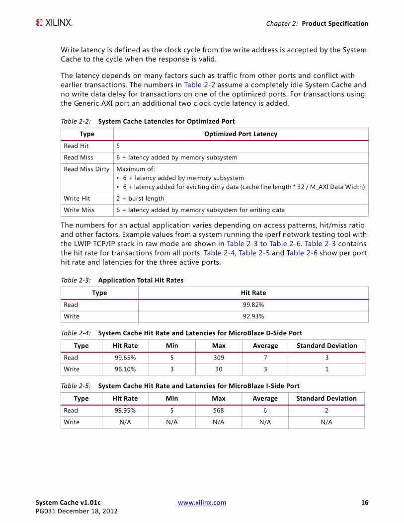
Write latency is defined as the clock cycle from the write address is accepted by the System Cache to the cycle when the response is valid.
The latency depends on many factors such as traff ic from other ports and conflict with earlier transactions. The numbers in Table 2-2 assume a completely idle System Cache and no write data delay for transactions on one of the optimized ports. For transactions using the Generic AXI port an additional two clock cycle latency is added.
The numbers for an actual application varies depending on access patterns, hit/miss ratio and other factors. Example values from a system running the iperf network testing tool with the LWIP TCP/IP stack in raw mode are shown in Table 2-3 to Table 2-6. Table 2-3 contains the hit rate for transactions from all ports. Table 2-4, Table 2-5 and Table 2-6 show per port hit rate and latencies for the three active ports.
Table 2-2: System Cache Latencies for Optimized Port
Type Optimized Port Latency
Read Hit 5
Read Miss 6 + latency added by memory subsystem
Read Miss Dirty Maximum of:• 6 + latency added by memory subsystem• 6 + latency added for evicting dirty data (cache line length * 32 / M_AXI Data Width)
Write Hit 2 + burst length
Write Miss 6 + latency added by memory subsystem for writing data
Table 2-3: Application Total Hit Rates
Type Hit Rate
Read 99.82%
Write 92.93%
Table 2-4: System Cache Hit Rate and Latencies for MicroBlaze D-Side Port
Type Hit Rate Min Max Average Standard Deviation
Read 99.65% 5 309 7 3
Write 96.10% 3 30 3 1
Table 2-5: System Cache Hit Rate and Latencies for MicroBlaze I-Side Port
Type Hit Rate Min Max Average Standard Deviation
Read 99.95% 5 568 6 2
Write N/A N/A N/A N/A N/A
System Cache v1.01c www.xilinx.com 17PG031 December 18, 2012
Chapter 2: Product Specification
ThroughputThe System Cache is fully pipelined and can have a theoretical maximum transaction rate of one read or write hit data concurrent with one read and one write miss data per clock cycle when there are no conflicts with earlier transactions.
This theoretical limit is subject to memory subsystem bandwidth, intra-transaction conflicts and cache hit detection overhead, which reduce the achieved throughput to less than three data beats per clock cycle.
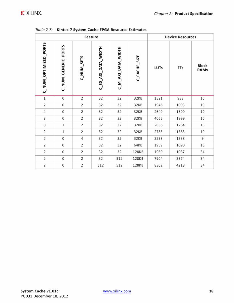
Resource UtilizationResources required for the System Cache core have been estimated for the Kintex™-7 FPGA (Table 2-7). These values were generated using the Xilinx® ISE® tools, version 14.4. They are derived from post-synthesis reports, and might be changed by MAP and PAR.
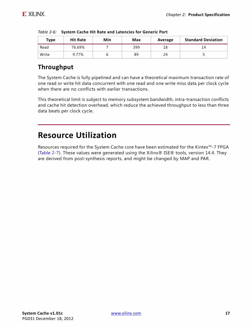
Table 2-6: System Cache Hit Rate and Latencies for Generic Port
Type Hit Rate Min Max Average Standard Deviation
Read 76.69% 7 399 18 14
Write 9.77% 6 89 24 5
System Cache v1.01c www.xilinx.com 18PG031 December 18, 2012
Chapter 2: Product Specification
Table 2-7: Kintex-7 System Cache FPGA Resource Estimates
Feature Device Resources
C_N
UM
_OPT
IMIZ
ED_P
ORT
S
C_N
UM
_GEN
ERIC
_PO
RTS
C_N
UM
_SET
S
C_S0
_AXI
_DAT
A_W
IDTH
C_M
_AXI
_DAT
A_W
IDTH
C_CA
CHE_
SIZE
LUTs FFs Block RAMs
1 0 2 32 32 32KB 1521 938 10
2 0 2 32 32 32KB 1946 1093 10
4 0 2 32 32 32KB 2649 1399 10
8 0 2 32 32 32KB 4065 1999 10
0 1 2 32 32 32KB 2036 1264 10
2 1 2 32 32 32KB 2785 1583 10
2 0 4 32 32 32KB 2298 1338 9
2 0 2 32 32 64KB 1959 1090 18
2 0 2 32 32 128KB 1960 1087 34
2 0 2 32 512 128KB 7904 3374 34
2 0 2 512 512 128KB 8302 4218 34
System Cache v1.01c www.xilinx.com 19PG031 December 18, 2012
Chapter 2: Product Specification
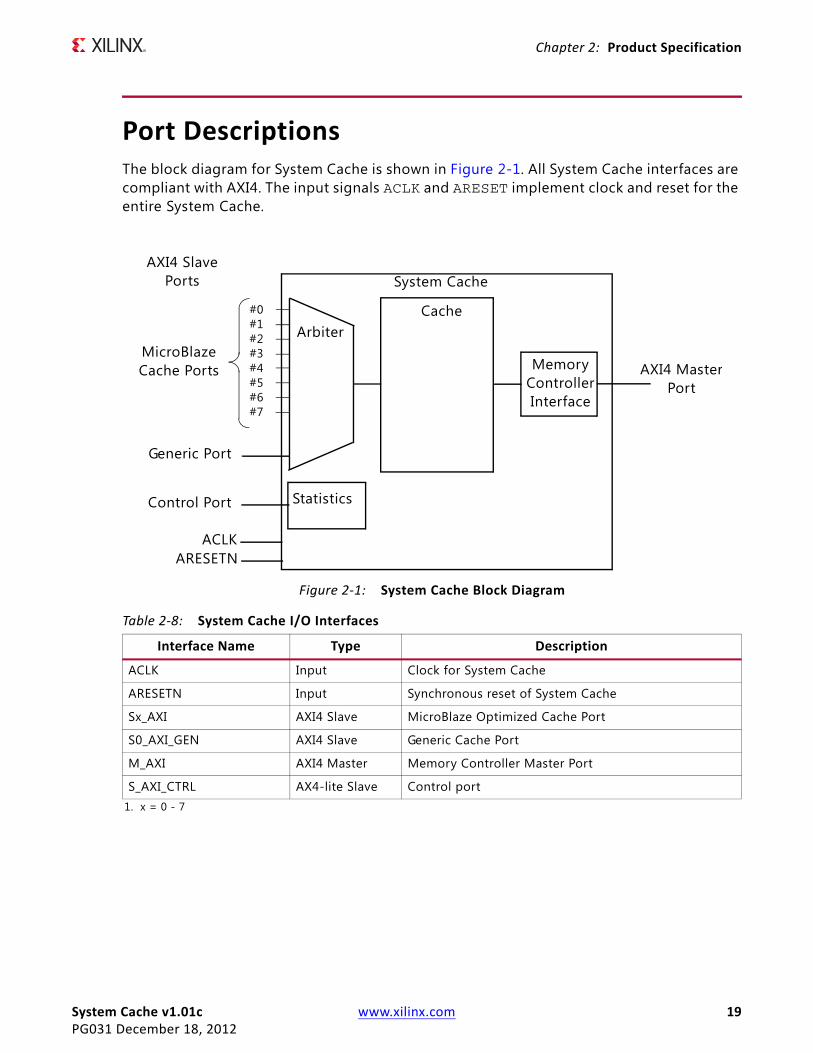
Port DescriptionsThe block diagram for System Cache is shown in Figure 2-1. All System Cache interfaces are compliant with AXI4. The input signals ACLK and ARESET implement clock and reset for the entire System Cache.
X-Ref Target - Figure 2-1
Figure 2-1: System Cache Block Diagram
Table 2-8: System Cache I/O Interfaces
Interface Name Type Description
ACLK Input Clock for System Cache
ARESETN Input Synchronous reset of System Cache
Sx_AXI AXI4 Slave MicroBlaze Optimized Cache Port
S0_AXI_GEN AXI4 Slave Generic Cache Port
M_AXI AXI4 Master Memory Controller Master Port
S_AXI_CTRL AX4-lite Slave Control port1. x = 0 - 7
Memory Controller Interface
Cache
Generic Port
MicroBlaze Cache Ports
#0#1#2#3#4#5#6#7
Arbiter
System CacheAXI4 Slave
Ports
AXI4 MasterPort
Control Port
ACLKARESETN
Statistics
System Cache v1.01c www.xilinx.com 20PG031 December 18, 2012
Chapter 2: Product Specification
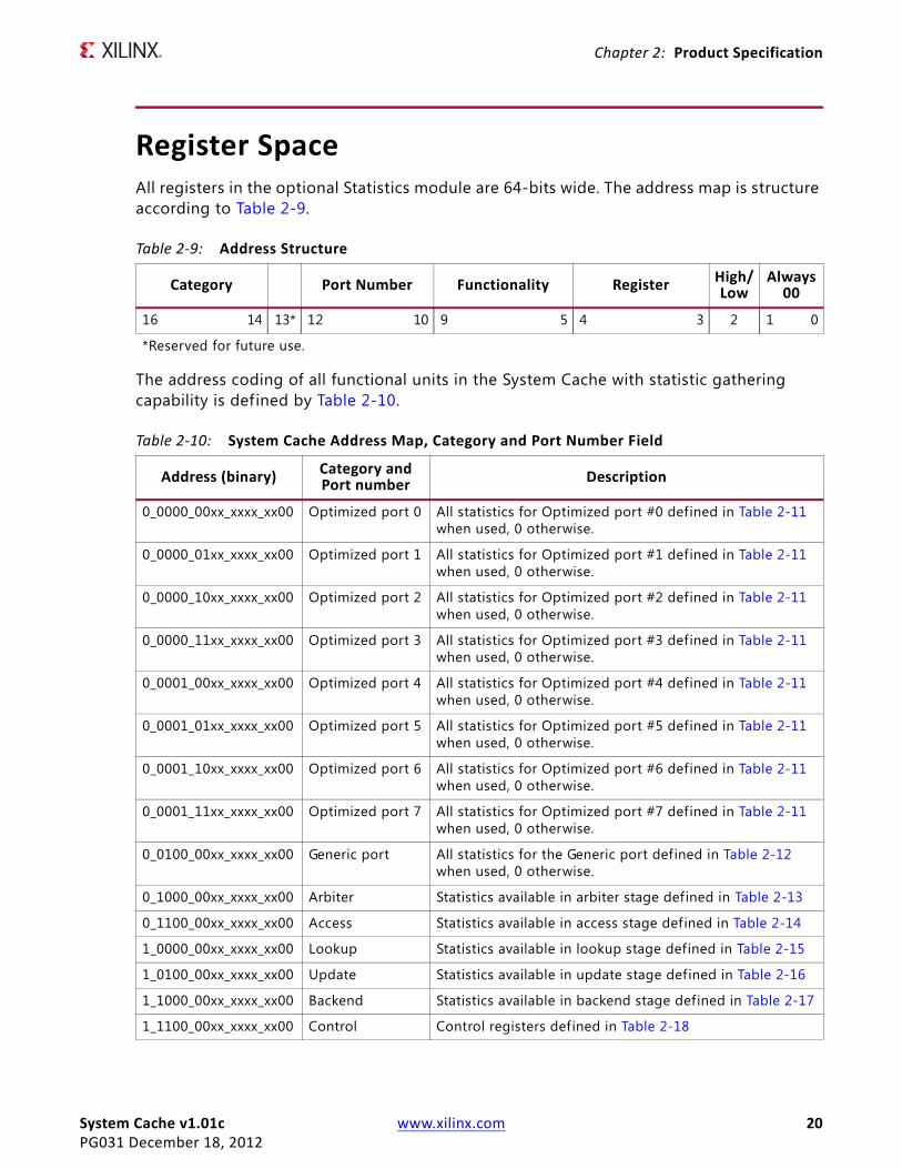
Register SpaceAll registers in the optional Statistics module are 64-bits wide. The address map is structure according to Table 2-9.
The address coding of all functional units in the System Cache with statistic gathering capability is defined by Table 2-10.
Table 2-9: Address Structure
Category Port Number Functionality Register High/Low
Always 00
16 14 13* 12 10 9 5 4 3 2 1 0
*Reserved for future use.
Table 2-10: System Cache Address Map, Category and Port Number Field
Address (binary) Category and Port number Description
0_0000_00xx_xxxx_xx00 Optimized port 0 All statistics for Optimized port #0 defined in Table 2-11 when used, 0 otherwise.
0_0000_01xx_xxxx_xx00 Optimized port 1 All statistics for Optimized port #1 defined in Table 2-11 when used, 0 otherwise.
0_0000_10xx_xxxx_xx00 Optimized port 2 All statistics for Optimized port #2 defined in Table 2-11 when used, 0 otherwise.
0_0000_11xx_xxxx_xx00 Optimized port 3 All statistics for Optimized port #3 defined in Table 2-11 when used, 0 otherwise.
0_0001_00xx_xxxx_xx00 Optimized port 4 All statistics for Optimized port #4 defined in Table 2-11 when used, 0 otherwise.
0_0001_01xx_xxxx_xx00 Optimized port 5 All statistics for Optimized port #5 defined in Table 2-11 when used, 0 otherwise.
0_0001_10xx_xxxx_xx00 Optimized port 6 All statistics for Optimized port #6 defined in Table 2-11 when used, 0 otherwise.
0_0001_11xx_xxxx_xx00 Optimized port 7 All statistics for Optimized port #7 defined in Table 2-11 when used, 0 otherwise.
0_0100_00xx_xxxx_xx00 Generic port All statistics for the Generic port defined in Table 2-12 when used, 0 otherwise.
0_1000_00xx_xxxx_xx00 Arbiter Statistics available in arbiter stage defined in Table 2-13
0_1100_00xx_xxxx_xx00 Access Statistics available in access stage defined in Table 2-14
1_0000_00xx_xxxx_xx00 Lookup Statistics available in lookup stage defined in Table 2-15
1_0100_00xx_xxxx_xx00 Update Statistics available in update stage defined in Table 2-16
1_1000_00xx_xxxx_xx00 Backend Statistics available in backend stage defined in Table 2-17
1_1100_00xx_xxxx_xx00 Control Control registers defined in Table 2-18
System Cache v1.01c www.xilinx.com 21PG031 December 18, 2012
Chapter 2: Product Specification
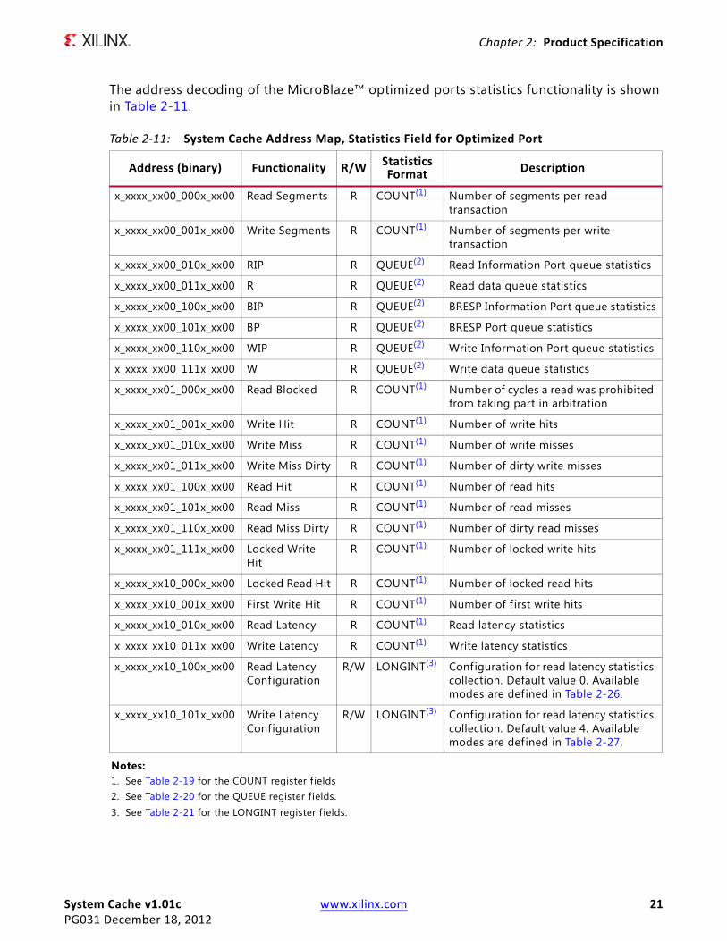
The address decoding of the MicroBlaze™ optimized ports statistics functionality is shown in Table 2-11.
Table 2-11: System Cache Address Map, Statistics Field for Optimized Port
Address (binary) Functionality R/W StatisticsFormat Description
x_xxxx_xx00_000x_xx00 Read Segments R COUNT(1) Number of segments per read transaction
x_xxxx_xx00_001x_xx00 Write Segments R COUNT(1) Number of segments per write transaction
x_xxxx_xx00_010x_xx00 RIP R QUEUE(2) Read Information Port queue statistics
x_xxxx_xx00_011x_xx00 R R QUEUE(2) Read data queue statistics
x_xxxx_xx00_100x_xx00 BIP R QUEUE(2) BRESP Information Port queue statistics
x_xxxx_xx00_101x_xx00 BP R QUEUE(2) BRESP Port queue statistics
x_xxxx_xx00_110x_xx00 WIP R QUEUE(2) Write Information Port queue statistics
x_xxxx_xx00_111x_xx00 W R QUEUE(2) Write data queue statistics
x_xxxx_xx01_000x_xx00 Read Blocked R COUNT(1) Number of cycles a read was prohibited from taking part in arbitration
x_xxxx_xx01_001x_xx00 Write Hit R COUNT(1) Number of write hits
x_xxxx_xx01_010x_xx00 Write Miss R COUNT(1) Number of write misses
x_xxxx_xx01_011x_xx00 Write Miss Dirty R COUNT(1) Number of dirty write misses
x_xxxx_xx01_100x_xx00 Read Hit R COUNT(1) Number of read hits
x_xxxx_xx01_101x_xx00 Read Miss R COUNT(1) Number of read misses
x_xxxx_xx01_110x_xx00 Read Miss Dirty R COUNT(1) Number of dirty read misses
x_xxxx_xx01_111x_xx00 Locked Write Hit
R COUNT(1) Number of locked write hits
x_xxxx_xx10_000x_xx00 Locked Read Hit R COUNT(1) Number of locked read hits
x_xxxx_xx10_001x_xx00 First Write Hit R COUNT(1) Number of f irst write hits
x_xxxx_xx10_010x_xx00 Read Latency R COUNT(1) Read latency statistics
x_xxxx_xx10_011x_xx00 Write Latency R COUNT(1) Write latency statistics
x_xxxx_xx10_100x_xx00 Read LatencyConfiguration
R/W LONGINT(3) Configuration for read latency statistics collection. Default value 0. Available modes are defined in Table 2-26.
x_xxxx_xx10_101x_xx00 Write LatencyConfiguration
R/W LONGINT(3) Configuration for read latency statistics collection. Default value 4. Available modes are defined in Table 2-27.
Notes: 1. See Table 2-19 for the COUNT register f ields2. See Table 2-20 for the QUEUE register f ields.3. See Table 2-21 for the LONGINT register f ields.
System Cache v1.01c www.xilinx.com 22PG031 December 18, 2012
Chapter 2: Product Specification
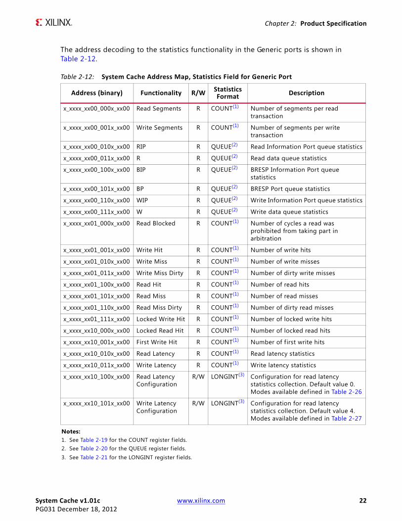
The address decoding to the statistics functionality in the Generic ports is shown in Table 2-12.
Table 2-12: System Cache Address Map, Statistics Field for Generic Port
Address (binary) Functionality R/W Statistics Format Description
x_xxxx_xx00_000x_xx00 Read Segments R COUNT(1) Number of segments per read transaction
x_xxxx_xx00_001x_xx00 Write Segments R COUNT(1) Number of segments per write transaction
x_xxxx_xx00_010x_xx00 RIP R QUEUE(2) Read Information Port queue statistics
x_xxxx_xx00_011x_xx00 R R QUEUE(2) Read data queue statistics
x_xxxx_xx00_100x_xx00 BIP R QUEUE(2) BRESP Information Port queue statistics
x_xxxx_xx00_101x_xx00 BP R QUEUE(2) BRESP Port queue statistics
x_xxxx_xx00_110x_xx00 WIP R QUEUE(2) Write Information Port queue statistics
x_xxxx_xx00_111x_xx00 W R QUEUE(2) Write data queue statistics
x_xxxx_xx01_000x_xx00 Read Blocked R COUNT(1) Number of cycles a read was prohibited from taking part in arbitration
x_xxxx_xx01_001x_xx00 Write Hit R COUNT(1) Number of write hits
x_xxxx_xx01_010x_xx00 Write Miss R COUNT(1) Number of write misses
x_xxxx_xx01_011x_xx00 Write Miss Dirty R COUNT(1) Number of dirty write misses
x_xxxx_xx01_100x_xx00 Read Hit R COUNT(1) Number of read hits
x_xxxx_xx01_101x_xx00 Read Miss R COUNT(1) Number of read misses
x_xxxx_xx01_110x_xx00 Read Miss Dirty R COUNT(1) Number of dirty read misses
x_xxxx_xx01_111x_xx00 Locked Write Hit R COUNT(1) Number of locked write hits
x_xxxx_xx10_000x_xx00 Locked Read Hit R COUNT(1) Number of locked read hits
x_xxxx_xx10_001x_xx00 First Write Hit R COUNT(1) Number of f irst write hits
x_xxxx_xx10_010x_xx00 Read Latency R COUNT(1) Read latency statistics
x_xxxx_xx10_011x_xx00 Write Latency R COUNT(1) Write latency statistics
x_xxxx_xx10_100x_xx00 Read LatencyConfiguration
R/W LONGINT(3) Configuration for read latency statistics collection. Default value 0. Modes available defined in Table 2-26
x_xxxx_xx10_101x_xx00 Write LatencyConfiguration
R/W LONGINT(3) Configuration for read latency statistics collection. Default value 4. Modes available defined in Table 2-27
Notes: 1. See Table 2-19 for the COUNT register f ields.2. See Table 2-20 for the QUEUE register f ields.3. See Table 2-21 for the LONGINT register f ields.
System Cache v1.01c www.xilinx.com 23PG031 December 18, 2012
Chapter 2: Product Specification
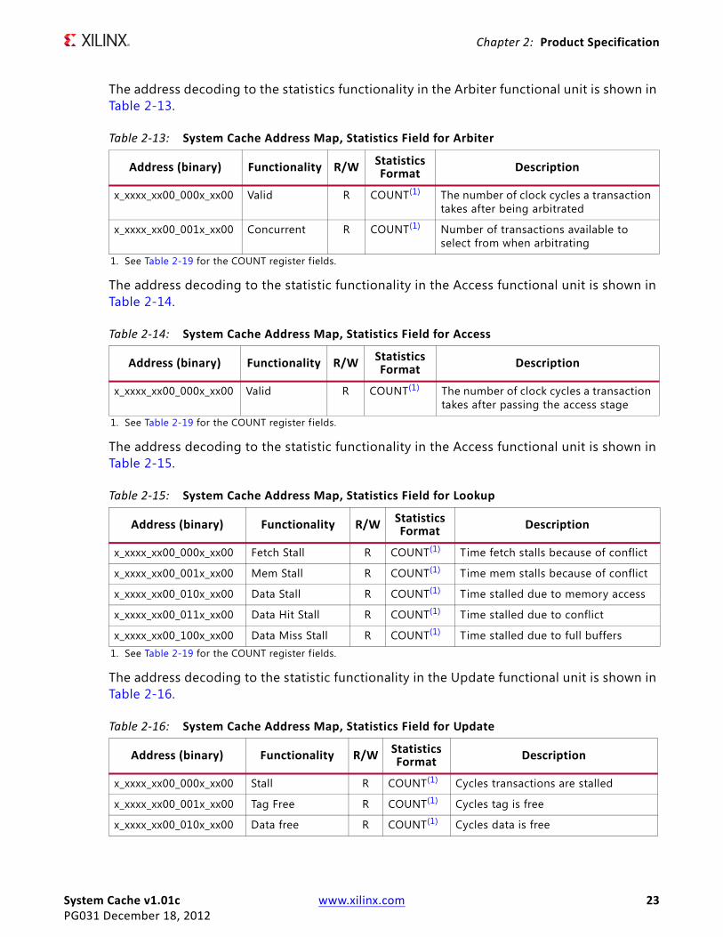
The address decoding to the statistics functionality in the Arbiter functional unit is shown in Table 2-13.
The address decoding to the statistic functionality in the Access functional unit is shown in Table 2-14.
The address decoding to the statistic functionality in the Access functional unit is shown in Table 2-15.
The address decoding to the statistic functionality in the Update functional unit is shown in Table 2-16.
Table 2-13: System Cache Address Map, Statistics Field for Arbiter
Address (binary) Functionality R/W Statistics Format Description
x_xxxx_xx00_000x_xx00 Valid R COUNT(1) The number of clock cycles a transaction takes after being arbitrated
x_xxxx_xx00_001x_xx00 Concurrent R COUNT(1) Number of transactions available to select from when arbitrating
1. See Table 2-19 for the COUNT register f ields.
Table 2-14: System Cache Address Map, Statistics Field for Access
Address (binary) Functionality R/W Statistics Format Description
x_xxxx_xx00_000x_xx00 Valid R COUNT(1) The number of clock cycles a transaction takes after passing the access stage
1. See Table 2-19 for the COUNT register f ields.
Table 2-15: System Cache Address Map, Statistics Field for Lookup
Address (binary) Functionality R/W Statistics Format Description
x_xxxx_xx00_000x_xx00 Fetch Stall R COUNT(1) Time fetch stalls because of conflict
x_xxxx_xx00_001x_xx00 Mem Stall R COUNT(1) Time mem stalls because of conflict
x_xxxx_xx00_010x_xx00 Data Stall R COUNT(1) Time stalled due to memory access
x_xxxx_xx00_011x_xx00 Data Hit Stall R COUNT(1) Time stalled due to conflict
x_xxxx_xx00_100x_xx00 Data Miss Stall R COUNT(1) Time stalled due to full buffers1. See Table 2-19 for the COUNT register f ields.
Table 2-16: System Cache Address Map, Statistics Field for Update
Address (binary) Functionality R/W Statistics Format Description
x_xxxx_xx00_000x_xx00 Stall R COUNT(1) Cycles transactions are stalled
x_xxxx_xx00_001x_xx00 Tag Free R COUNT(1) Cycles tag is free
x_xxxx_xx00_010x_xx00 Data free R COUNT(1) Cycles data is free
System Cache v1.01c www.xilinx.com 24PG031 December 18, 2012
Chapter 2: Product Specification
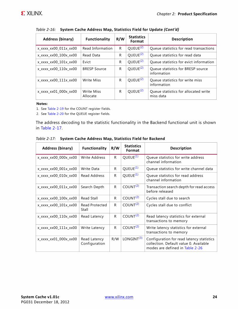
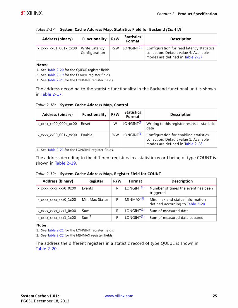
The address decoding to the statistic functionality in the Backend functional unit is shown in Table 2-17.
x_xxxx_xx00_011x_xx00 Read Information R QUEUE(2) Queue statistics for read transactions
x_xxxx_xx00_100x_xx00 Read Data R QUEUE(2) Queue statistics for read data
x_xxxx_xx00_101x_xx00 Evict R QUEUE(2) Queue statistics for evict information
x_xxxx_xx00_110x_xx00 BRESP Source R QUEUE(2) Queue statistics for BRESP source information
x_xxxx_xx00_111x_xx00 Write Miss R QUEUE(2) Queue statistics for write miss information
x_xxxx_xx01_000x_xx00 Write Miss Allocate
R QUEUE(2) Queue statistics for allocated write miss data
Notes: 1. See Table 2-19 for the COUNT register f ields.2. See Table 2-20 for the QUEUE register f ields.
Table 2-17: System Cache Address Map, Statistics Field for Backend
Address (binary) Functionality R/W StatisticsFormat Description
x_xxxx_xx00_000x_xx00 Write Address R QUEUE(1) Queue statistics for write address channel information
x_xxxx_xx00_001x_xx00 Write Data R QUEUE(1) Queue statistics for write channel data
x_xxxx_xx00_010x_xx00 Read Address R QUEUE(1) Queue statistics for read address channel information
x_xxxx_xx00_011x_xx00 Search Depth R COUNT(2) Transaction search depth for read access before released
x_xxxx_xx00_100x_xx00 Read Stall R COUNT(2) Cycles stall due to search
x_xxxx_xx00_101x_xx00 Read Protected Stall
R COUNT(2) Cycles stall due to conflict
x_xxxx_xx00_110x_xx00 Read Latency R COUNT(2) Read latency statistics for external transactions to memory
x_xxxx_xx00_111x_xx00 Write Latency R COUNT(2) Write latency statistics for external transactions to memory
x_xxxx_xx01_000x_xx00 Read Latency Configuration
R/W LONGINT(3) Configuration for read latency statistics collection. Default value 0. Available modes are defined in Table 2-26
Table 2-16: System Cache Address Map, Statistics Field for Update (Cont’d)
Address (binary) Functionality R/W Statistics Format Description
System Cache v1.01c www.xilinx.com 25PG031 December 18, 2012
Chapter 2: Product Specification
The address decoding to the statistic functionality in the Backend functional unit is shown in Table 2-17.
The address decoding to the different registers in a statistic record being of type COUNT is shown in Table 2-19.
The address the different registers in a statistic record of type QUEUE is shown in Table 2-20.
x_xxxx_xx01_001x_xx00 Write Latency Configuration
R/W LONGINT(3) Configuration for read latency statistics collection. Default value 4. Available modes are defined in Table 2-27
Notes: 1. See Table 2-20 for the QUEUE register f ields.2. See Table 2-19 for the COUNT register f ields.3. See Table 2-21 for the LONGINT register f ields.
Table 2-18: System Cache Address Map, Control
Address (binary) Functionality R/W StatisticsFormat Description
x_xxxx_xx00_000x_xx00 Reset W LONGINT(1) Writing to this register resets all statistic data
x_xxxx_xx00_001x_xx00 Enable R/W LONGINT(1) Configuration for enabling statistics collection. Default value 1. Available modes are defined in Table 2-28
1. See Table 2-21 for the LONGINT register f ields.
Table 2-19: System Cache Address Map, Register Field for COUNT
Address (binary) Register R/W Format Description
x_xxxx_xxxx_xxx0_0x00 Events R LONGINT(1) Number of times the event has been triggered
x_xxxx_xxxx_xxx0_1x00 Min Max Status R MINMAX(2) Min, max and status information defined according to Table 2-24
x_xxxx_xxxx_xxx1_0x00 Sum R LONGINT(1) Sum of measured data
x_xxxx_xxxx_xxx1_1x00 Sum2 R LONGINT(1) Sum of measured data squared
Notes: 1. See Table 2-21 for the LONGINT register f ields.2. See Table 2-22 for the MINMAX register f ields.
Table 2-17: System Cache Address Map, Statistics Field for Backend (Cont’d)
Address (binary) Functionality R/W StatisticsFormat Description
System Cache v1.01c www.xilinx.com 26PG031 December 18, 2012
Chapter 2: Product Specification
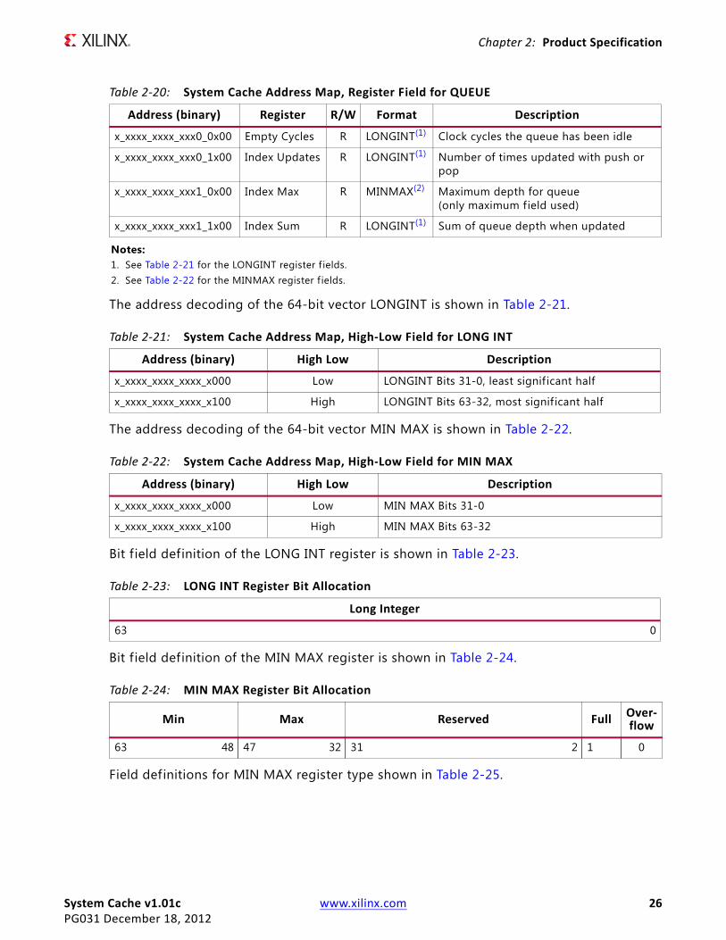
The address decoding of the 64-bit vector LONGINT is shown in Table 2-21.
The address decoding of the 64-bit vector MIN MAX is shown in Table 2-22.
Bit f ield definition of the LONG INT register is shown in Table 2-23.
Bit f ield definition of the MIN MAX register is shown in Table 2-24.
Field definitions for MIN MAX register type shown in Table 2-25.
Table 2-20: System Cache Address Map, Register Field for QUEUE
Address (binary) Register R/W Format Description
x_xxxx_xxxx_xxx0_0x00 Empty Cycles R LONGINT(1) Clock cycles the queue has been idle
x_xxxx_xxxx_xxx0_1x00 Index Updates R LONGINT(1) Number of times updated with push or pop
x_xxxx_xxxx_xxx1_0x00 Index Max R MINMAX(2) Maximum depth for queue(only maximum field used)
x_xxxx_xxxx_xxx1_1x00 Index Sum R LONGINT(1) Sum of queue depth when updated
Notes: 1. See Table 2-21 for the LONGINT register f ields.2. See Table 2-22 for the MINMAX register f ields.
Table 2-21: System Cache Address Map, High-Low Field for LONG INT
Address (binary) High Low Description
x_xxxx_xxxx_xxxx_x000 Low LONGINT Bits 31-0, least signif icant half
x_xxxx_xxxx_xxxx_x100 High LONGINT Bits 63-32, most signif icant half
Table 2-22: System Cache Address Map, High-Low Field for MIN MAX
Address (binary) High Low Description
x_xxxx_xxxx_xxxx_x000 Low MIN MAX Bits 31-0
x_xxxx_xxxx_xxxx_x100 High MIN MAX Bits 63-32
Table 2-23: LONG INT Register Bit Allocation
Long Integer
63 0
Table 2-24: MIN MAX Register Bit Allocation
Min Max Reserved Full Over-flow
63 48 47 32 31 2 1 0
System Cache v1.01c www.xilinx.com 27PG031 December 18, 2012
Chapter 2: Product Specification
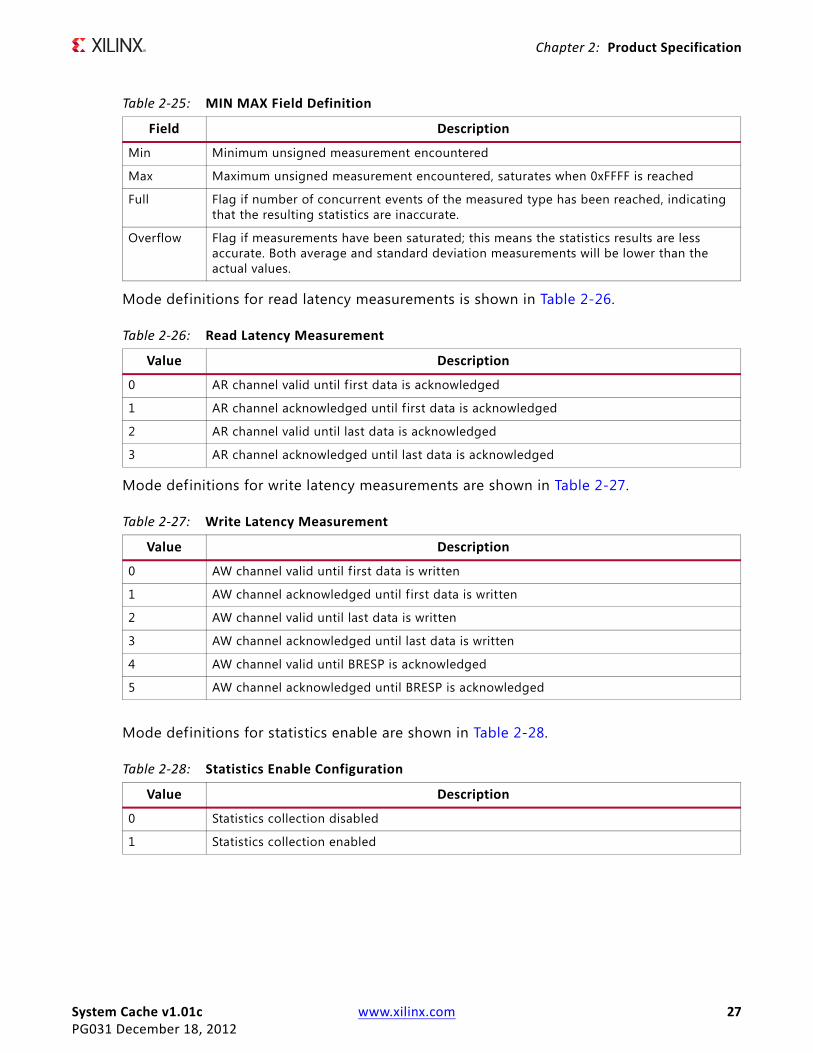
Mode definitions for read latency measurements is shown in Table 2-26.
Mode definitions for write latency measurements are shown in Table 2-27.
Mode definitions for statistics enable are shown in Table 2-28.
Table 2-25: MIN MAX Field Definition
Field Description
Min Minimum unsigned measurement encountered
Max Maximum unsigned measurement encountered, saturates when 0xFFFF is reached
Full Flag if number of concurrent events of the measured type has been reached, indicating that the resulting statistics are inaccurate.
Overflow Flag if measurements have been saturated; this means the statistics results are less accurate. Both average and standard deviation measurements will be lower than the actual values.
Table 2-26: Read Latency Measurement
Value Description
0 AR channel valid until f irst data is acknowledged
1 AR channel acknowledged until f irst data is acknowledged
2 AR channel valid until last data is acknowledged
3 AR channel acknowledged until last data is acknowledged
Table 2-27: Write Latency Measurement
Value Description
0 AW channel valid until f irst data is written
1 AW channel acknowledged until f irst data is written
2 AW channel valid until last data is written
3 AW channel acknowledged until last data is written
4 AW channel valid until BRESP is acknowledged
5 AW channel acknowledged until BRESP is acknowledged
Table 2-28: Statistics Enable Configuration
Value Description
0 Statistics collection disabled
1 Statistics collection enabled
System Cache v1.01c www.xilinx.com 28PG031 December 18, 2012
Chapter 3
Designing with the CoreThis chapter includes guidelines and additional information to facilitate designing with the core.
General Design GuidelinesThe are no golden settings to achieve maximum performance for all cases, as performance is application and system dependent. This chapter contains general guidelines for consideration when configuring System Cache and other IP cores to improve performance.
AXI Data WidthsAXI Data widths should match wherever possible. Matching widths results in minimal area overhead and latency for the AXI interconnects.
AXI ClockingThe System Cache is fully synchronous. Using the same clock for all the AXI ports removes the need for clock conversion blocks and results in minimal area overhead and latency for the AXI interconnects.
Frequency and Hit RateIncreased cache hit rate results in higher performance.
The System Cache size should be configured to be larger than the connected L1 caches to achieve any improvements. Increasing the System Cache size increases hit rate and have a positive effect on performance. The downside of increasing the System Cache size is an increased number of FPGA resources being used. Higher set associativity usually increase the hit rate and the application performance.
The maximum frequency of MicroBlaze™ is affected by its cache sizes. Smaller MicroBlaze cache sizes usually means that MicroBlaze can meet higher frequency targets. The sweet spot for the frequency versus cache size trade-off when using the System Cache occurs when configuring MicroBlaze caches to either 256 or 512 bytes, depending on other
System Cache v1.01c www.xilinx.com 29PG031 December 18, 2012
Chapter 3: Designing with the Core
MicroBlaze configuration settings. The key to improve frequency is to implement MicroBlaze cache tags with distributed RAM.
Enabling the MicroBlaze Branch Target Cache can improve performance but might reduce the maximum obtainable frequency. Depending on the rest of the MicroBlaze configuration smaller BTC sizes, such as 32 entries (C_BRANCH_TARGET_CACHE_SIZE = 3), should be considered.
Enabling MicroBlaze victim caches increases MicroBlaze cache hit rates, with improved performance as a result. Enabling victim caches can however reduce MicroBlaze maximum frequency in some cases. Instruction stream cache should be disabled, because it usually reduces performance when connected to System Cache. MicroBlaze performance is often improved by using 8-word cache lines on the Instruction Cache and Data Cache.
BandwidthUsing wider AXI interfaces increases data bandwidth, but also increases FPGA resource usage. Using the widest possible common AXI data width between the System Cache AXI Master and the external memory gives the highest possible bandwidth. This also applies to the AXI connection between MicroBlaze caches and the System Cache. The widest possible common width gives the highest bandwidth.
ArbitrationThe System Cache arbitration scheme is round-robin. When the selected port does not have a pending transaction, the f irst port with an available transaction is scheduled, considering the optimized ports in ascending numeric order and finally the generic port.
Only one read request per port is processed at a time. While one port has a read in progress no other reads from the same port are scheduled. A write from any port or read from any other port with no read in progress can be arbitrated during this time.
ClockingThe System Cache is fully synchronous with all interfaces and the internal function clocked by the ACLK input signal. It is advisable to avoid asynchronous clock transitions in the system as they add latency and consumes area resources.
System Cache v1.01c www.xilinx.com 30PG031 December 18, 2012
Chapter 3: Designing with the Core
ResetsThe System Cache is reset by the ARESETN input signal. ARESETN is synchronous to ACLK and needs be asserted one ACLK cycle to take affect. The System Cache is ready for operation two ACLK cycles after ARESETN is deasserted.
Protocol DescriptionAll interfaces to the System Cache adhere to the AXI4 protocol.
System Cache v1.01c www.xilinx.com 31PG031 December 18, 2012
SECTION II: VIVADO DESIGN SUITE
Customizing and Generating the Core
Constraining the Core
System Cache v1.01c www.xilinx.com 32PG031 December 18, 2012
Chapter 4
Customizing and Generating the CoreThis chapter includes information on using Xilinx® tools to customize and generate the core in the Vivado™ Design Suite.
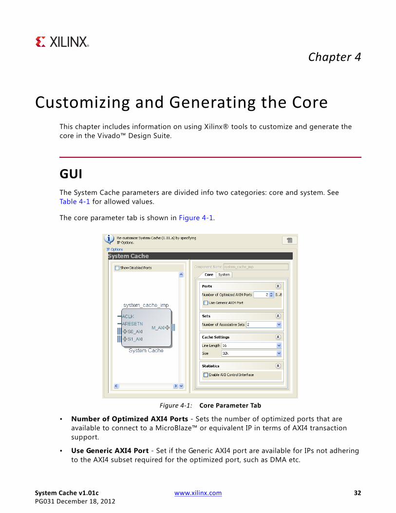
GUIThe System Cache parameters are divided info two categories: core and system. See Table 4-1 for allowed values.
The core parameter tab is shown in Figure 4-1.
• Number of Optimized AXI4 Ports - Sets the number of optimized ports that are available to connect to a MicroBlaze™ or equivalent IP in terms of AXI4 transaction support.
• Use Generic AXI4 Port - Set if the Generic AXI4 port are available for IPs not adhering to the AXI4 subset required for the optimized port, such as DMA etc.
X-Ref Target - Figure 4-1
Figure 4-1: Core Parameter Tab
System Cache v1.01c www.xilinx.com 33PG031 December 18, 2012
Chapter 4: Customizing and Generating the Core
• Number of Associative Sets - Specify how many sets the associativity uses.
• Line Length - System Cache cache line length is f ixed to 16.
• Size - Sets the size of the System Cache in bytes.
• Enable AXI Control Interface - Set if statistics interface is available.
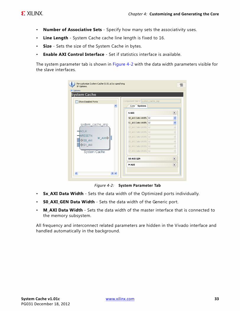
The system parameter tab is shown in Figure 4-2 with the data width parameters visible for the slave interfaces.
• Sx_AXI Data Width - Sets the data width of the Optimized ports individually.
• S0_AXI_GEN Data Width - Sets the data width of the Generic port.
• M_AXI Data Width - Sets the data width of the master interface that is connected to the memory subsystem.
All frequency and interconnect related parameters are hidden in the Vivado interface and handled automatically in the background.
X-Ref Target - Figure 4-2
Figure 4-2: System Parameter Tab
System Cache v1.01c www.xilinx.com 34PG031 December 18, 2012
Chapter 4: Customizing and Generating the Core
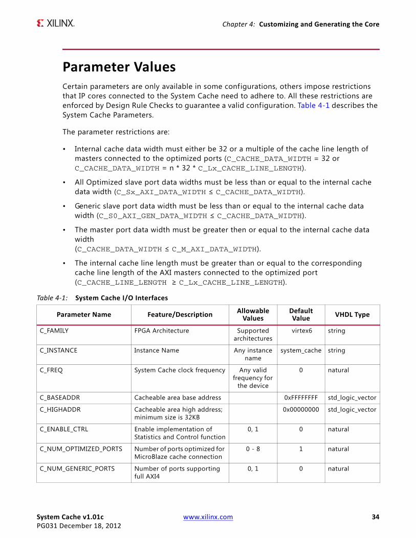
Parameter ValuesCertain parameters are only available in some configurations, others impose restrictions that IP cores connected to the System Cache need to adhere to. All these restrictions are enforced by Design Rule Checks to guarantee a valid configuration. Table 4-1 describes the System Cache Parameters.
The parameter restrictions are:
• Internal cache data width must either be 32 or a multiple of the cache line length of masters connected to the optimized ports (C_CACHE_DATA_WIDTH = 32 or C_CACHE_DATA_WIDTH = n * 32 * C_Lx_CACHE_LINE_LENGTH).
• All Optimized slave port data widths must be less than or equal to the internal cache data width (C_Sx_AXI_DATA_WIDTH ≤ C_CACHE_DATA_WIDTH).
• Generic slave port data width must be less than or equal to the internal cache data width (C_S0_AXI_GEN_DATA_WIDTH ≤ C_CACHE_DATA_WIDTH).
• The master port data width must be greater then or equal to the internal cache data width(C_CACHE_DATA_WIDTH ≤ C_M_AXI_DATA_WIDTH).
• The internal cache line length must be greater than or equal to the corresponding cache line length of the AXI masters connected to the optimized port (C_CACHE_LINE_LENGTH ≥ C_Lx_CACHE_LINE_LENGTH).
Table 4-1: System Cache I/O Interfaces
Parameter Name Feature/Description AllowableValues
DefaultValue VHDL Type
C_FAMILY FPGA Architecture Supportedarchitectures
virtex6 string
C_INSTANCE Instance Name Any instancename
system_cache string
C_FREQ System Cache clock frequency Any valid frequency for
the device
0 natural
C_BASEADDR Cacheable area base address 0xFFFFFFFF std_logic_vector
C_HIGHADDR Cacheable area high address; minimum size is 32KB
0x00000000 std_logic_vector
C_ENABLE_CTRL Enable implementation of Statistics and Control function
0, 1 0 natural
C_NUM_OPTIMIZED_PORTS Number of ports optimized for MicroBlaze cache connection
0 - 8 1 natural
C_NUM_GENERIC_PORTS Number of ports supporting full AXI4
0, 1 0 natural
System Cache v1.01c www.xilinx.com 35PG031 December 18, 2012
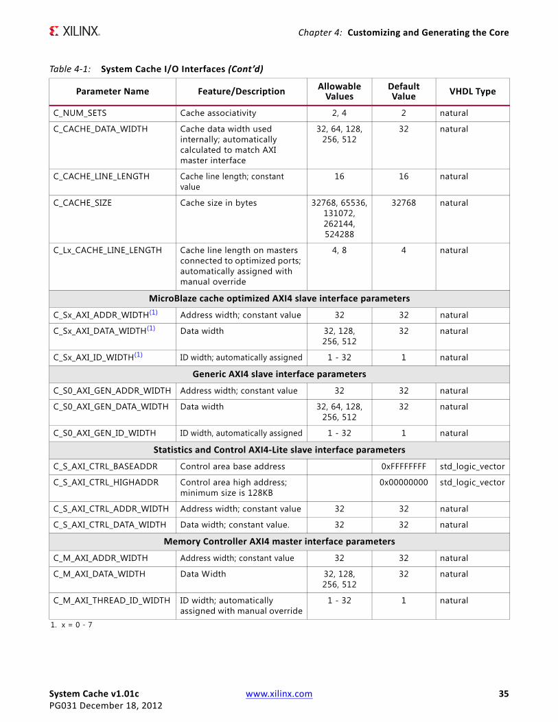
Chapter 4: Customizing and Generating the Core
C_NUM_SETS Cache associativity 2, 4 2 natural
C_CACHE_DATA_WIDTH Cache data width used internally; automatically calculated to match AXI master interface
32, 64, 128,256, 512
32 natural
C_CACHE_LINE_LENGTH Cache line length; constant value
16 16 natural
C_CACHE_SIZE Cache size in bytes 32768, 65536,131072, 262144, 524288
32768 natural
C_Lx_CACHE_LINE_LENGTH Cache line length on masters connected to optimized ports; automatically assigned with manual override
4, 8 4 natural
MicroBlaze cache optimized AXI4 slave interface parameters
C_Sx_AXI_ADDR_WIDTH(1) Address width; constant value 32 32 natural
C_Sx_AXI_DATA_WIDTH(1) Data width 32, 128, 256, 512
32 natural
C_Sx_AXI_ID_WIDTH(1) ID width; automatically assigned 1 - 32 1 natural
Generic AXI4 slave interface parameters
C_S0_AXI_GEN_ADDR_WIDTH Address width; constant value 32 32 natural
C_S0_AXI_GEN_DATA_WIDTH Data width 32, 64, 128,256, 512
32 natural
C_S0_AXI_GEN_ID_WIDTH ID width, automatically assigned 1 - 32 1 natural
Statistics and Control AXI4-Lite slave interface parameters
C_S_AXI_CTRL_BASEADDR Control area base address 0xFFFFFFFF std_logic_vector
C_S_AXI_CTRL_HIGHADDR Control area high address; minimum size is 128KB
0x00000000 std_logic_vector
C_S_AXI_CTRL_ADDR_WIDTH Address width; constant value 32 32 natural
C_S_AXI_CTRL_DATA_WIDTH Data width; constant value. 32 32 natural
Memory Controller AXI4 master interface parameters
C_M_AXI_ADDR_WIDTH Address width; constant value 32 32 natural
C_M_AXI_DATA_WIDTH Data Width 32, 128, 256, 512
32 natural
C_M_AXI_THREAD_ID_WIDTH ID width; automatically assigned with manual override
1 - 32 1 natural
1. x = 0 - 7
Table 4-1: System Cache I/O Interfaces (Cont’d)
Parameter Name Feature/Description AllowableValues
DefaultValue VHDL Type
System Cache v1.01c www.xilinx.com 36PG031 December 18, 2012
Chapter 5
Constraining the Core
Required ConstraintsThere are no required constraints for this core.
Device, Package, and Speed Grade SelectionsThere are no Device, Package or Speed Grade requirements for this core.
Clock FrequenciesThere are no specific clock frequency requirements for this core.
Clock ManagementThere are no specific clock management requirements for this core.
Clock PlacementThere are no specific Clock placement requirements for this core.
BankingThere are no specific Banking rules for this core.
System Cache v1.01c www.xilinx.com 37PG031 December 18, 2012
Chapter 5: Constraining the Core
Transceiver PlacementThere are no Transceiver Placement requirements for this core.
I/O Standard and PlacementThere are no specific I/O standards and placement requirements for this core.
System Cache v1.01c www.xilinx.com 38PG031 December 18, 2012
SECTION III: ISE DESIGN SUITE
Customizing and Generating the Core
Constraining the Core
System Cache v1.01c www.xilinx.com 39PG031 December 18, 2012
Chapter 6
Customizing and Generating the CoreThis chapter includes information on using Xilinx® tools to customize and generate the core in the ISE® Design Suite.
GUIThe System Cache parameters are divided info three categories: core, system and interconnect related. See Table 4-1 for allowed values.
The core parameter tab is shown in Figure 6-1.
• Number of Optimized AXI4 Ports - Sets the number of optimized ports that are available to connect to a MicroBlaze™ or equivalent IP in terms of AXI4 transaction support.
• Use Generic AXI4 Port - Set if the Generic AXI4 port are available for IPs not adhering to the AXI4 subset required for the optimized port, such as DMA etc.
X-Ref Target - Figure 6-1
Figure 6-1: Core Parameter Tab
System Cache v1.01c www.xilinx.com 40PG031 December 18, 2012
Chapter 6: Customizing and Generating the Core
• Number of Associative Sets - Specify how many sets the associativity uses.
• Data Width - Internal data width is automatically calculated from the M_AXI interface.
• Line Length - System Cache cache line length is f ixed to 16.
• Size - Sets the size of the System Cache in bytes.
• Enable AXI Control Interface - Set if statistics interface is available.
The system parameter tab is shown in Figure 6-2 with the address parameters and S0 interface parameters visible.
• Base/High Address - Sets the address range for the cacheable area.
• Control Interface Base/High Address - Sets the address range for the control interface area that contains all statistics and control registers. Only available when the control interface is enabled.
• Sx_AXI Data Width - Sets the data width of the Optimized ports individually.
• S0_AXI_GEN Data Width - Sets the data width of the Generic port.
• M_AXI Data Width - Sets the data width of the master interface that is connected to the memory subsystem.
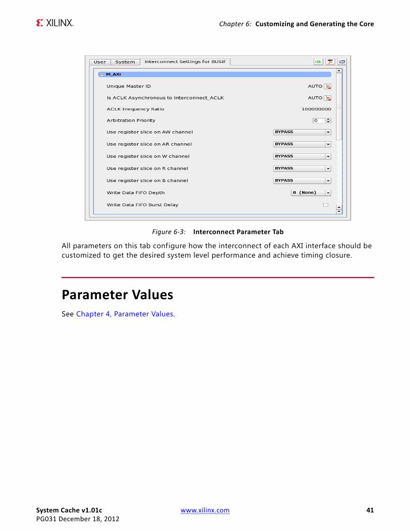
The interconnect parameter tab is shown in Figure 6-3, showing the first few parameters.
X-Ref Target - Figure 6-2
Figure 6-2: System Parameter Tab
System Cache v1.01c www.xilinx.com 41PG031 December 18, 2012
Chapter 6: Customizing and Generating the Core
All parameters on this tab configure how the interconnect of each AXI interface should be customized to get the desired system level performance and achieve timing closure.
Parameter ValuesSee Chapter 4, Parameter Values.
X-Ref Target - Figure 6-3
Figure 6-3: Interconnect Parameter Tab
System Cache v1.01c www.xilinx.com 42PG031 December 18, 2012
Chapter 7
Constraining the CoreThere are no constraints associated with this core.
System Cache v1.01c www.xilinx.com 43PG031 December 18, 2012
SECTION IV: APPENDICES
Migrating
Debugging
Application Software Development
Additional Resources
System Cache v1.01c www.xilinx.com 44PG031 December 18, 2012
Appendix A
MigratingThis appendix describes migrating from older versions of the IP to the current IP release.
For information on migrating to the Vivado™ Design Suite, see the Vivado Design Suite Migration Methodology Guide [Ref 4].
Port ChangesNo changes needed.
Functionality ChangesThe supported cache sizes has been increased to support 256KB and 512KB.
Hit and miss statistics are changed to be on a per port basis instead of total.
System Cache v1.01c www.xilinx.com 45PG031 December 18, 2012
Appendix B
DebuggingThis appendix includes details about resources available on the Xilinx Support website and debugging tools. In addition, this appendix provides a step-by-step debugging process and a flow diagram to guide you through debugging the System Cache core.
The following topics are included in this appendix:
• Finding Help on Xilinx.com
• Debug Tools
• Simulation Debug
• Hardware Debug
• Interface Debug
Finding Help on Xilinx.comTo help in the design and debug process when using the System Cache, the Xilinx Support web page (www.xilinx.com/support) contains key resources such as product documentation, release notes, answer records, information about known issues, and links for opening a Technical Support WebCase.
DocumentationThis product guide is the main document associated with the System Cache. This guide, along with documentation related to all products that aid in the design process, can be found on the Xilinx Support web page (www.xilinx.com/support) or by using the Xilinx Documentation Navigator.
Download the Xilinx Documentation Navigator from the Design Tools tab on the Downloads page (www.xilinx.com/download). For more information about this tool and the features available, open the online help after installation.
System Cache v1.01c www.xilinx.com 46PG031 December 18, 2012
Appendix B: Debugging
Release NotesKnown issues for all cores, including the System Cache are described in the IP Release Notes Guide (XTP025).
Contacting Technical SupportXilinx provides premier technical support for customers encountering issues that require additional assistance.
To contact Xilinx Technical Support:
1. Navigate to www.xilinx.com/support.
2. Open a WebCase by selecting the WebCase link located under Support Quick Links.
When opening a WebCase, include:
• Target FPGA including package and speed grade.
• All applicable Xilinx Design Tools and simulator software versions.
• Additional f iles based on the specif ic issue might also be required. See the relevant sections in this debug guide for guidelines about which f ile(s) to include with the WebCase.
Debug Tools
ChipScope Pro ToolThe ChipScope™ Pro debugging tool inserts logic analyzer, bus analyzer, and virtual I/O cores directly into your design. The ChipScope Pro debugging tool allows you to set trigger conditions to capture application and integrated block port signals in hardware. Captured signals can then be analyzed through the ChipScope Pro logic analyzer tool. For detailed information for using the ChipScope Pro debugging tool, see www.xilinx.com/tools/cspro.htm.
Reference BoardsAll Xilinx development boards for Spartan6, Virtex6 and 7 series FPGAs support System Cache. These boards can be used to prototype designs and establish that the core can communicate with the system.
System Cache v1.01c www.xilinx.com 47PG031 December 18, 2012
Appendix B: Debugging
Simulation DebugThe simulation debug flow for ModelSim is described below. A similar approach can be used with other simulators.
• Check for the latest supported versions of ModelSim in the Xilinx Design Tools: Release Notes Guide. Is this version being used? If not, update to this version.
• If using Verilog, do you have a mixed mode simulation license? If not, obtain a mixed-mode license.
• Ensure that the proper libraries are compiled and mapped. In Xilinx Platform Studio this is done within the tool using Edit → Preferences → Simulation, and in the Vivado Design Suite using Flow → Simulation Settings.
• Have you associated the intended software program for all connected MicroBlaze™ processor with the simulation? Use Project → Select Elf File in Xilinx Platform Studio to do this. Make sure to regenerate the simulation files with Simulation → Generate Simulation HDL Files afterwards. The equivalent command in the Vivado Design Suite is Tools → Associate ELF Files.
• When observing the traffic on any of the AXI interfaces connected to the System Cache, see the AMBA® AXI and ACE Protocol Specification [Ref 2] for the AXI timing.
Hardware DebugThis section provides debug steps for common issues. The ChipScope debugging tool and Vivado Lab Tools are valuable resources to use in hardware debug.
Many of these common issues can also be applied to debugging design simulations. Details are provided on:
• General Checks
• AXI Checks
General ChecksEnsure that all the timing constraints for the core were properly incorporated from the example design and that all constraints were met during implementation.
• Does it work in post-place and route timing simulation? If problems are seen in hardware but not in timing simulation, this could indicate a PCB issue. Ensure that all clock sources are active and clean.
System Cache v1.01c www.xilinx.com 48PG031 December 18, 2012
Appendix B: Debugging
• If using MMCMs in the design, ensure that all MMCMs have obtained lock by monitoring the LOCKED port.
AXI ChecksEither use bus analyzer or connect the relevant AXI signals to a logic analyzer in ChipScope or Vivado Lab Tools. Make sure the data is captured with ACLK.
Interface Debug
Optimized AXI4 InterfacesOnly the number of ports specified by C_NUM_OPTIMIZED_PORTS are available. There are no registers to read, but basic functionality is tested by writing data and then reading it back. Output S<x>_AXI_AWREADY asserts when the write address is used, S<x>_AXI_WREADY asserts when the write data is used, and output S<x>_AXI_BVALID asserts when the write response is valid. Output S<x>_AXI_ARREADY asserts when the read address is used, and output S<x>_AXI_RVALID asserts when the read data/response is valid. If the interface is unresponsive, ensure that the following conditions are met:
• The ACLK input is connected and toggling.
• The interface is not being held in reset, and ARESETN is an active-Low reset.
• Make sure the accessed Optimized port is activated.
• If the simulation has been run, verify in simulation and/or a ChipScope debugging tool capture that the waveform is correct for accessing the AXI4 interface.
Generic AXI4 InterfacesThe Generic ports is only available when C_NUM_GENERIC_PORTS is set to one. There are no registers to read, but basic functionality is tested by writing data and then reading it back. Output S0_AXI_GEN_AWREADY asserts when the write address is used, S0_AXI_GEN_WREADY asserts when the write data is used, and output S0_AXI_GEN_BVALID asserts when the write response is valid. Output S0_AXI_GEN_ARREADY asserts when the read address is used, and output S0_AXI_GEN_RVALID asserts when the read data/response is valid. If the interface is unresponsive, ensure that the following conditions are met:
• The ACLK input is connected and toggling.
• The interface is not being held in reset, and ARESETN is an active-Low reset.
• Make sure the Generic port is activated.
System Cache v1.01c www.xilinx.com 49PG031 December 18, 2012
Appendix B: Debugging
• If the simulation has been run, verify in simulation and/or a ChipScope debugging tool capture that the waveform is correct for accessing the AXI4 interface.
AXI4-Lite InterfacesThe AXI4-Lite interface is only available when the Control interface is enabled with C_ENABLE_CTRL. Read from a register that does not have all 0s as a default to verify that the interface is functional. Output S_AXI_CTRL_ARREADY asserts when the read address is used, and output S_AXI_CTRL_RVALID asserts when the read data/response is valid. If the interface is unresponsive, ensure that the following conditions are met:
• The ACLK input is connected and toggling.
• The interface is not being held in reset, and ARESETN is an active-Low reset.
• If the simulation has been run, verify in simulation and/or a ChipScope debugging tool capture that the waveform is correct for accessing the AXI4-Lite interface.
System Cache v1.01c www.xilinx.com 50PG031 December 18, 2012
Appendix C
Application Software Development
Device DriversThere is no specific driver for System Cache; it is transparent from an application point of view.
System Cache v1.01c www.xilinx.com 51PG031 December 18, 2012
Appendix D
Additional Resources
Xilinx ResourcesFor support resources such as Answers, Documentation, Downloads, and Forums, see the Xilinx Support website at:
www.xilinx.com/support.
For a glossary of technical terms used in Xilinx documentation, see:
www.xilinx.com/company/terms.htm.
ReferencesThese documents provide supplemental material useful with this product guide:
1. AMBA® 4 AXI4-Stream Protocol Specif ication v1.0 (ARM IHI 0051A)
2. AMBA® AXI and ACE Protocol Specification (ARM IHI 0022D)
3. Vivado™ Design Suite user documentation
4. Vivado™ Design Suite Migration Methodology Guide (UG911)
System Cache v1.01c www.xilinx.com 52PG031 December 18, 2012
Appendix D: Additional Resources
Technical SupportXilinx provides technical support at www.xilinx.com/support for this LogiCORE™ IP product when used as described in the product documentation. Xilinx cannot guarantee timing, functionality, or support of product if implemented in devices that are not defined in the documentation, if customized beyond that allowed in the product documentation, or if changes are made to any section of the design labeled DO NOT MODIFY.
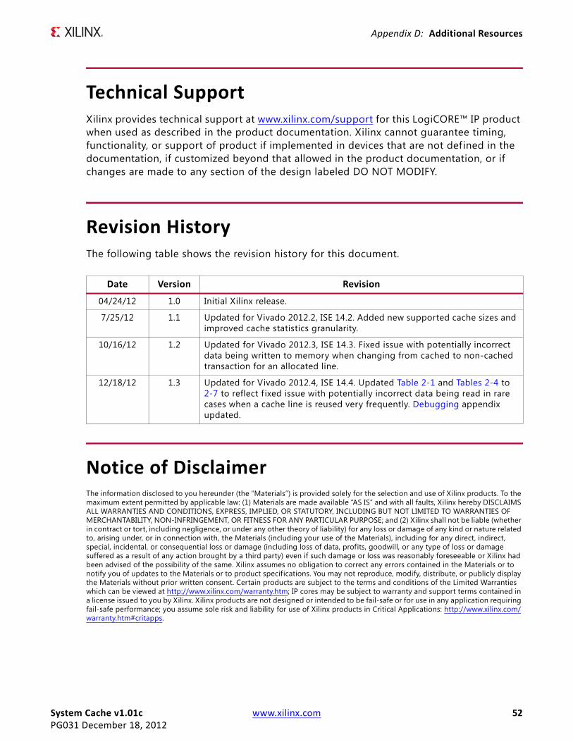
Revision HistoryThe following table shows the revision history for this document.
Notice of DisclaimerThe information disclosed to you hereunder (the “Materials”) is provided solely for the selection and use of Xilinx products. To the maximum extent permitted by applicable law: (1) Materials are made available “AS IS” and with all faults, Xilinx hereby DISCLAIMS ALL WARRANTIES AND CONDITIONS, EXPRESS, IMPLIED, OR STATUTORY, INCLUDING BUT NOT LIMITED TO WARRANTIES OF MERCHANTABILITY, NON-INFRINGEMENT, OR FITNESS FOR ANY PARTICULAR PURPOSE; and (2) Xilinx shall not be liable (whether in contract or tort, including negligence, or under any other theory of liability) for any loss or damage of any kind or nature related to, arising under, or in connection with, the Materials (including your use of the Materials), including for any direct, indirect, special, incidental, or consequential loss or damage (including loss of data, profits, goodwill, or any type of loss or damage suffered as a result of any action brought by a third party) even if such damage or loss was reasonably foreseeable or Xilinx had been advised of the possibility of the same. Xilinx assumes no obligation to correct any errors contained in the Materials or to notify you of updates to the Materials or to product specifications. You may not reproduce, modify, distribute, or publicly display the Materials without prior written consent. Certain products are subject to the terms and conditions of the Limited Warranties which can be viewed at http://www.xilinx.com/warranty.htm; IP cores may be subject to warranty and support terms contained in a license issued to you by Xilinx. Xilinx products are not designed or intended to be fail-safe or for use in any application requiring fail-safe performance; you assume sole risk and liability for use of Xilinx products in Critical Applications: http://www.xilinx.com/warranty.htm#critapps.
Date Version Revision
04/24/12 1.0 Initial Xilinx release.
7/25/12 1.1 Updated for Vivado 2012.2, ISE 14.2. Added new supported cache sizes and improved cache statistics granularity.
10/16/12 1.2 Updated for Vivado 2012.3, ISE 14.3. Fixed issue with potentially incorrect data being written to memory when changing from cached to non-cached transaction for an allocated line.
12/18/12 1.3 Updated for Vivado 2012.4, ISE 14.4. Updated Table 2-1 and Tables 2-4 to 2-7 to reflect f ixed issue with potentially incorrect data being read in rare cases when a cache line is reused very frequently. Debugging appendix updated.
System Cache v1.01c www.xilinx.com 53PG031 December 18, 2012
Appendix D: Additional Resources
Automotive Applications DisclaimerXILINX PRODUCTS ARE NOT DESIGNED OR INTENDED TO BE FAIL-SAFE, OR FOR USE IN ANY APPLICATION REQUIRING FAIL-SAFE PERFORMANCE, SUCH AS APPLICATIONS RELATED TO: (I) THE DEPLOYMENT OF AIRBAGS, (II) CONTROL OF A VEHICLE, UNLESS THERE IS A FAIL-SAFE OR REDUNDANCY FEATURE (WHICH DOES NOT INCLUDE USE OF SOFTWARE IN THE XILINX DEVICE TO IMPLEMENT THE REDUNDANCY) AND A WARNING SIGNAL UPON FAILURE TO THE OPERATOR, OR (III) USES THAT COULD LEAD TO DEATH OR PERSONAL INJURY. CUSTOMER ASSUMES THE SOLE RISK AND LIABILITY OF ANY USE OF XILINX PRODUCTS IN SUCH APPLICATIONS.© Copyright 2012 Xilinx, Inc. Xilinx, the Xilinx logo, Artix, ISE, Kintex, Spartan, Virtex, Vivado, Zynq, and other designated brands included herein are trademarks of Xilinx in the United States and other countries. ARM is a registered trademark of ARM in the EU and other countries The AMBA trademark is a registered trademark or ARM Limited. All other trademarks are the property of their respective owners.