logicore ip peak cancellation crest factor reduction v3 v3.0.pdf · multi-user and multi-carrier...
TRANSCRIPT

DS846 June 22, 2011 www.xilinx.com 1Product Specification
© Copyright 2011 Xilinx, Inc. Xilinx, the Xilinx logo, Artix, ISE, Kintex, Spartan, Virtex, Zynq, and other designated brands included herein are trademarks of Xilinx in the United States and other countries. ARM is a registered trademark of ARM in the EU and other countries. The AMBA trademark is a registered trademark of ARM Limited. MATLAB is a registered trademark of The MathWorks, Inc. All other trademarks are the property of their respective owners.
IntroductionCrest Factor Reduction (CFR) is used to limit thedynamic range of the signals being transmitted inWireless Communications and other applications.Multi-user and multi-carrier signals often have a highpeak-to-average ratio (PAR). This places high demandson the data converters and especially limits theefficiency of operation of the Power Amplifiers (PAs)used in cellular base stations. Reducing the PAR istherefore beneficial in increasing PA efficiency byallowing higher average power to be transmittedbefore saturation occurs.
Features• Multiple air interface standards supported -
MC-GSM, WCDMA, TD-SCDMA, WiMAX, LTE, CDMA2000, Mixed mode (for example, GSM + LTE, TD-SCDMA + LTE, WCDMA + LTE)
• Tx BW support of up to 145 MHz
• Various multi-carrier configurations supported
• Meets performance requirements (EVM, PAPR and ACLR) of all air interfaces
• Configurable clock-to-sample ratio of 1 to 4 for resource optimization
• Configurable number of Cancellation Pulse Generators (CPGs) of 1 to 8 per iteration
• Multiple antenna support for 1, 2, 4 and 8 antennas
• Multiple iteration support for 1 to 8 iterations
• Variable quantization support for 11 to 18 bits
• Configurable latency support for 66 to 10106 samples
• User-selectable cancellation pulse loading mode: single-pulse fixed coefficients, single-pulse configurable coefficients, two-pulses configurable coefficients
• Cancellation pulse read back support (in configurable coefficients modes only)
• AXI4-Stream compliant for data interface and AXI4-Lite compliant for control interface
• MATLAB® simulator available for system-level verification
• Bit accurate C model available
LogiCORE IP Peak CancellationCrest Factor Reduction v3.0
DS846 June 22, 2011 Product Specification
LogiCORE IP Facts Table
Core Specifics
Supported Device Family(1)
Virtex-7, Kintex-7, Artix-7, Zynq-7000,Virtex-6, Spartan-6
Supported User Interfaces AXI4-Stream, AXI4-Lite
Resources(2) Freq.
Configuration LUTs FFs Slices DSPSlices
BlockRAMs(3)
Max.Freq.(4)
ANT=1,ITER=1,CPS=1,CPG=4 1822 2198 843 18 4/3 350
ANT=1,ITER=1,CPS=2,CPG=4 1573 1850 734 10 2/3 370
ANT=1,ITER=1,CPS=3,CPG=6 1766 2006 920 10 2/3 380
ANT=1,ITER=1,CPS=4,CPG=4 1465 1681 691 6 1/3 390
Provided with Core
DocumentationProduct Brief
Product SpecificationC Model User Guide
Design Files Netlist
Example Design Not Provided
Test Bench VHDL
Constraints File Not Provided
Simulation Model Verilog, VHDL, C Model and MATLAB Model
Tested Design Tools
Design Entry Tools CORE Generator 13.2
Simulation(5) Mentor Graphics ModelSimISim
Synthesis Tools XST 13.2
Support
Provided by Xilinx, Inc.1. For a complete listing of supported devices, see the release notes for this
core.2. Resources listed here are for Kintex-7 devices. For more complete
device performance numbers, see Table 19 to 22.3. Based on 36K/18K block RAMs4. Performance numbers listed are for Kintex-7 FPGAs. For more complete
performance data, see Resource Requirements and Performance, page 34.
5. For the supported version of the tools, see the ISE Design Suite 13: Release Notes Guide
DS846 June 22, 2011 www.xilinx.com 2Product Specification
LogiCORE IP Peak Cancellation Crest Factor Reduction v3.0
OverviewCrest Factor Reduction (CFR) is used to limit the dynamic range of the signals being transmitted in WirelessCommunications and other applications. Multi-user and multi-carrier signals often have a high peak-to-averageratio (PAR). This places high demands on the data converters and especially limits the efficiency of operation of thePower Amplifiers (PAs) used in cellular base stations. Reducing the PAR is therefore beneficial in increasing PAefficiency by allowing higher average power to be transmitted before saturation occurs.
In a modern transmit chain, CFR is also often incorporated with Digital Predistortion (DPD), which acts to linearizethe PA, allowing operation at maximum efficiency with spectral compliance. CFR is helpful to DPD because it levelsthe signal peaks, making accurate correction estimation easier [Ref 1].
The Xilinx® PC-CFR core is an efficient, flexible and easy-to-use implementation that supports Virtex®-7,Kintex™-7, Artix™-7, Zynq™-7000, Virtex-6, and Spartan®-6 FPGA families. It is configurable both in function, tosupport all major cellular wireless air interfaces, and in usage, to support a variety of clocking and resourcerequirements.
Features and General DescriptionThe Peak Cancellation-CFR core processes control and data through industry-standard AXI4 interfaces that allowimmediate logic-free connection to other Xilinx IP components and to any general environment. The controlinterface is AXI4-Lite compliant and the data interface is AXI4-Stream compliant. The control interface providesaccess to a set of configuration registers and a pulse coefficients RAM and the data interface is used for streamingdata in/out of the core. The data flow is unidirectional with no rate or bit-width change. A typical CFR applicationconsists of multiple iterations and multiple antennas that can be configured through the GUI. The core is configuredfor a particular application through the control interface. In particular, the contents of the pulse coefficients RAMare related to the spectrum of the signal being transmitted. Later sections of this data sheet discuss the generalprinciples behind producing these coefficients, and specific details are given for the WCDMA, CDMA2000,WiMAX, TD-SCDMA, GSM and E-UTRAN (LTE) air interfaces. Mixed-mode signal operation is also supported.Pulse coefficients can be pre-configured at generation time through a .coe file or configured in operation via thecontrol interface. There is also provision for a shadow bank of coefficients to be loaded, and then activated with aselect signal, to cater to applications where fast dynamic switching is required. Functions that can be run withMATLAB® are supplied for simulation and design of the cancellation pulse.
The core can be configured for clock-to-sample ratios between 1 and 4, and for algorithmic complexity, allowingFPGA fabric resources to be minimized for a given application. The algorithmic complexity is the number ofhardware resources available to cancel the signal peaks. These are called Cancellation Pulse Generators.
Algorithm DescriptionMost practical CFR solutions are based in principle on subtracting a correction signal from the original signal asshown in Figure 1.

DS846 June 22, 2011 www.xilinx.com 3Product Specification
LogiCORE IP Peak Cancellation Crest Factor Reduction v3.0
The correction signal is a spectrally compliant signal that matches the signal peaks. For example, in Noise-shapingCFR [Ref 3] the correction signal is a filtered version of the signal after magnitude thresholding, that is, the signalabove a clipping threshold is filtered by a noise-shaping filter. In Peak Cancellation CFR, the correction signal is asum of individual cancellation pulses. The pulses are applied by searching for peaks in the signal. Each pulse is theimpulse response of a filter that is designed to match the spectral content of the signal. Figures 2, 3, and 4 depict thesequence of events. Figure 2 shows the detection of the peak and the identification of the excess amplitude overthreshold, (A - Ath). Figure 3 shows the cancellation pulse. This pulse is the appropriate unit magnitude impulseresponse scaled by CP_val = (A - Ath) * eϑ where ϑ is the phase.
That is to say, the cancellation pulse is scaled to the excess magnitude over the desired clipping threshold at thepeak with the phase of the signal at the peak. This is because the signals are complex and each cancellation pulsemust be rotated to match the phase of the corresponding signal peak. When the cancellation pulse is subtractedfrom the original signal, it reduces the signal peak magnitude to the threshold value, as indicated in Figure 4, whilepreserving the signal phase. For asymmetric spectra, the cancellation pulse itself is complex.
X-Ref Target - Figure 1
Figure 1: Generalized CFR Block Diagram
X-Ref Target - Figure 2
Figure 2: Peak Detection
Correction signal
Matching delay
DS750 02 102709

DS846 June 22, 2011 www.xilinx.com 4Product Specification
LogiCORE IP Peak Cancellation Crest Factor Reduction v3.0
In hardware, the cancellation pulse is generated by a cancellation pulse generator (CPG) with function as indicatedin Figure 5. The address counter must be triggered at the appropriate time to play out the pulse and the complexmultiplier factors in the correct scaling.
X-Ref Target - Figure 3
Figure 3: The Cancellation Pulse
X-Ref Target - Figure 4
Figure 4: Peak Cancellation

DS846 June 22, 2011 www.xilinx.com 5Product Specification
LogiCORE IP Peak Cancellation Crest Factor Reduction v3.0
The resource complexity of the PC-CFR core is bounded by having a finite number of cancellation pulses availableat any one time. This means that, depending on the signals, not all the peaks are guaranteed to be cancelled in onepass, so an application typically has multiple (identical) iterations.
A detailed structure for the PC-CFR core implementation is shown in Figure 6.
The Peak Detect block identifies the signal sample at which the magnitude is a maximum in a region where itexceeds the CFR Threshold, which is a register input. The Peak Scale block forms the complex value for thecancellation pulse as described previously. The Allocator block takes care of assigning CPGs to peaks. It has anAllocator Spacing as a register input. This restricts the frequency of peak assignment and is sometimes used toimprove EVM performance for certain signals, as discussed in the Applications section. The CPG pulse coefficientsRAM is as discussed in Features and General Description.
One of the key features of the peak cancellation method is that it is very flexible with respect to supporting differentair interfaces. Because the cancellation pulse coefficients are generated offline and then loaded into RAM, it ispossible to support a wide variety of carrier configurations and bandwidths using the same hardware.
X-Ref Target - Figure 5
Figure 5: Cancellation Pulse Generator
X-Ref Target - Figure 6
Figure 6: PC-CFR High-level Block View
Complex muliplier
pulse coefficients RAMAddress counter
CP_val
imre
re
im
re
im
DS750_03_102709
Peak Detect
Peak Scaling
Reduced PAR
Signal
High PAR
Signal
Allocator CPG # 1
Peak Locations
CPG # 2
CPG # N
Sum
× ×
×
Mag Phase
Delay
DS750_04_102709

DS846 June 22, 2011 www.xilinx.com 6Product Specification
LogiCORE IP Peak Cancellation Crest Factor Reduction v3.0
General Operation
Control Interface
The control interface is used for writing to the configuration registers and loading the pulse coefficients RAM. It isimplemented as an AXI4-Lite slave interface. The total memory space available is 64K locations, although only therequired memory locations are physically implemented in hardware. Even though the required address bus widthis only 16 bits, the core has a 32-bit address bus at the interface. Internally, the higher 16-bits (31-16) are ignored. Theaddress format and the memory map are given in Table 1 and Table 2 respectively.
The memory space is divided into 8 partitions (one for each antenna) of 8K locations each and bits 15-13 of theaddress (Ant Sel) are used to select the antenna. Each 8K partition is further divided into 2 partitions (configurationregisters and pulse coefficients RAM) of 4K locations each and bit 12 of the address (Reg/RAM Sel) is used for thisselection (0 -> configuration registers, 1 -> pulse coefficients RAM). The 4K locations of the pulse coefficients RAMcan store 2 pulses (for dynamic switching) of maximum length 2K each. The Maximum Cancellation Pulse Lengthparameter in the GUI is used to optimize block RAM resource usage based on the requirement. Bits 11-0 are used toaddress a specific configuration register or a specific location in the pulse coefficients RAM.
Table 1: Control Interface Address Format
Bit 31-16 Bits 15-13 Bit 12 Bit 11-0
Unused Ant Sel Reg/RAM Sel Offset
Table 2: Control Memory Map
Reg/RAM Sel Offset (hex) Register/
RAM Name Datawidth (bits) Description
0 0x000 Filter Length
9, 10 or 11 (depending on Max Cancellation Pulse Length = 511, 1023 or
2047)
Input to provide the number of filter taps. This controls the number of coefficient values that are read from memory. Valid only when configurable coefficients have been configured, as otherwise this value is inferred from the .coe file.
0 0x001 Filter Select 1Input to select which pulse is in use (0 = Pulse 0, 1= Pulse 1). Valid only when 'Two pulses (selectable) configurable coefficients' is selected.
0 0x002 Threshold 16 Input to provide the threshold level over which valid peaks can be identified.
0 0x003-0x00A
Allocator Spacing for iteration 1 to
8
10
Input to provide the minimum number of samples required between valid peaks in order for a cancellation pulse generator to be allocated. The core has an inherent minimum spacing of 2, so the actual value is the value specified plus 2.
10x000 - (Max
Cancellation Pulse Length-1)
Pulse 0Coefficients
RAM32
Memory to store Pulse 0 coefficients. Coefficients are stored as 16-bit I concatenated with 16-bit Q (Q in MSW, I In LSW).
1
(Max Cancellation Pulse Length+1)-
(2xMax Cancellation Pulse
Length)
Pulse 1Coefficients
RAM32
Memory to store Pulse 1 coefficients. Coefficients are stored as 16-bit I concatenated with 16-bit Q (Q in MSW, I In LSW).

DS846 June 22, 2011 www.xilinx.com 7Product Specification
LogiCORE IP Peak Cancellation Crest Factor Reduction v3.0
Configuration Registers
The configuration registers are defined in Table 2. These registers are typically programmed once at start-up andcan be changed dynamically if required. No attempt has been made to balance the pipelines of these registers to thedifferent parts of the circuit where they are applied. So if any of these registers are changed during normal coreoperation without applying a core reset (ARESETN), then transient behavior occurs at the output for up to (2300 xNo. of Iterations) samples. The configuration registers are write-only and cannot be read.
Pulse Coefficients RAM
The control interface is used to load the pulse coefficients RAM only when configurable coefficients are in use. Themaximum pulse coefficients address space available per antenna is 4K for the two-pulse setup. The actual blockRAM usage is based on the Maximum Cancellation Pulse Length parameter in the GUI. The pulse coefficients RAMcan also be read back through the control interface.
For write accesses, either both address and data can be written simultaneously, or one can be written before theother. In any case, the access is complete only after both address and data have been written and the write responsehas been received. The write response is a 2-bit signal indicating the success/failure of the current write access(00=OK, 1X=ERROR, 01=NA). It has a fixed latency of two cycles from the when the latest of address/data has beenaccepted on the input. Until the write response is received, the address and data ready signals are kept deassertedindicating that a new access cannot begin. Figure 7 shows the timing diagram for the write operation. The timingdiagram firstly shows the case where address and data are written simultaneously. Secondly it shows an addresswrite before the corresponding data, thirdly a data write before the corresponding address, and lastly a writeterminated by reset. There can be any delay between the address and data or the data and address where the writeoperations occur on different cycles. The reset operation shows a write being terminated after the address hasalready been written; write operations where the data has been written, but not the address, can also be terminatedusing reset. The reset latency is one cycle, that is, the core output signals (such as write address ready, write dataready, etc) return to their idle state one cycle after reset is deasserted. In all of the previous cases, the reset operationalso resets all the configuration registers (Filter Length, Filter Select, Threshold and Allocator Spacing), but does notreset the pulse coefficients RAM. Therefore the configuration registers need to be reloaded after a control resetoperation.
For read accesses, the address is written first and the access is complete after the read data/response has beenissued. The read response is a 2-bit data indicating the success/failure of the current read access (00=OK,1X=ERROR, 01=NA). It has a fixed latency of five cycles from the when the address has been accepted on the input.Until the read data/response is issued, the address ready signal is kept deasserted indicating that a new access
X-Ref Target - Figure 7
Figure 7: Control Write Timing Diagram
s_axi_aclk
s_axi_aresetn
s_axi_awvalid
s_axi_awready
s_axi_awaddr
s_axi_wvalid
s_axi_wready
s_axi_wdata
s_axi_bvalid
s_axi_bready
s_axi_bresp
A0 A1 A2 A3
D0 D1 D2
R0 R1 R2

DS846 June 22, 2011 www.xilinx.com 8Product Specification
LogiCORE IP Peak Cancellation Crest Factor Reduction v3.0
cannot begin. Figure 8 shows the timing diagram for the read operation. The reset operation shows a read beingterminated after the address has already been written. The reset latency is one cycle, i.e., the core output signals(such as read address ready, read data valid, etc) return to their normal state one cycle after reset is deasserted.
The core does not support burst accesses or simultaneous write and read accesses. An ongoing write/read accesshas to be completed/terminated before the next write/read access can begin.
Data Interface
The core supports multiple data-rates (1 to 4 clock-cycles/sample) on the AXI4-Stream interface throughREADY-VALID handshaking. After power-up or reset, the core is idle until S_AXIS_DIN_TVALID has beenasserted for the first time. S_AXIS_DIN_TREADY is asserted two cycles after reset deassertion and held high andM_AXIS_DOUT_TVALID is held low until S_AXIS_DIN_TVALID is asserted. After this, the core is synchronizedand expects data input and provides data output every x clock cycles defined by the configuration parameter"data-rate" in clock-cycles/sample. S_AXIS_DIN_TVALID could be asserted at the same time asS_AXIS_DIN_TREADY, asserted in advance, or held asserted between S_AXIS_DIN_TREADY assertions.
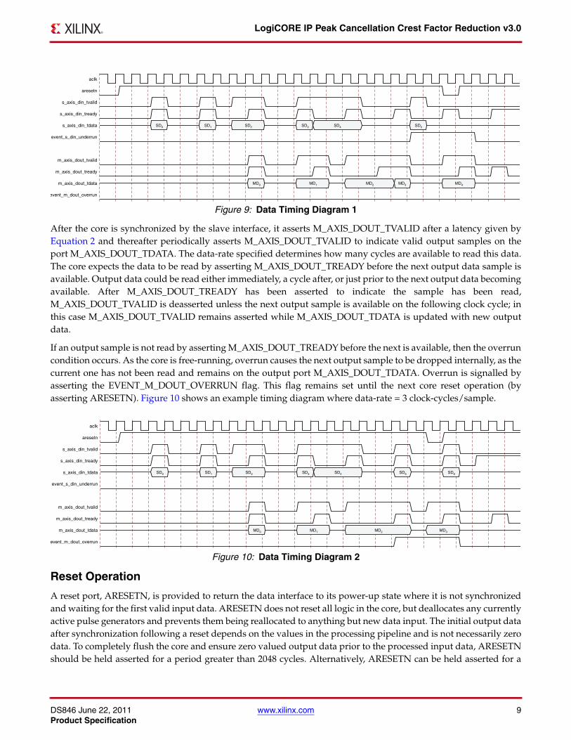
If S_AXIS_DIN_TVALID is not asserted when S_AXIS_DIN_TREADY is held high, then the underrun conditionoccurs because valid data was not available when the core expected it. As the core is free-running, underrun causesthe preceding data sample to be input for a second time internally. Underrun is signalled by asserting theEVENT_S_DIN_UNDERRUN flag. This flag remains set until the next core reset operation (by assertingARESETN). Figure 9 shows an example timing diagram where data-rate = 3 clock-cycles/sample.
X-Ref Target - Figure 8
Figure 8: Control Read Timing Diagram
s_axi_aclk
s_axi_aresetn
s_axi_arvalid
s_axi_arready
s_axi_araddr
s_axi_rvalid
s_axi_rready
s_axi_rdata
s_axi_rresp
A0 A1
D0
R0
DS846 June 22, 2011 www.xilinx.com 9Product Specification
LogiCORE IP Peak Cancellation Crest Factor Reduction v3.0
After the core is synchronized by the slave interface, it asserts M_AXIS_DOUT_TVALID after a latency given byEquation 2 and thereafter periodically asserts M_AXIS_DOUT_TVALID to indicate valid output samples on theport M_AXIS_DOUT_TDATA. The data-rate specified determines how many cycles are available to read this data.The core expects the data to be read by asserting M_AXIS_DOUT_TREADY before the next output data sample isavailable. Output data could be read either immediately, a cycle after, or just prior to the next output data becomingavailable. After M_AXIS_DOUT_TREADY has been asserted to indicate the sample has been read,M_AXIS_DOUT_TVALID is deasserted unless the next output sample is available on the following clock cycle; inthis case M_AXIS_DOUT_TVALID remains asserted while M_AXIS_DOUT_TDATA is updated with new outputdata.
If an output sample is not read by asserting M_AXIS_DOUT_TREADY before the next is available, then the overruncondition occurs. As the core is free-running, overrun causes the next output sample to be dropped internally, as thecurrent one has not been read and remains on the output port M_AXIS_DOUT_TDATA. Overrun is signalled byasserting the EVENT_M_DOUT_OVERRUN flag. This flag remains set until the next core reset operation (byasserting ARESETN). Figure 10 shows an example timing diagram where data-rate = 3 clock-cycles/sample.
Reset Operation
A reset port, ARESETN, is provided to return the data interface to its power-up state where it is not synchronizedand waiting for the first valid input data. ARESETN does not reset all logic in the core, but deallocates any currentlyactive pulse generators and prevents them being reallocated to anything but new data input. The initial output dataafter synchronization following a reset depends on the values in the processing pipeline and is not necessarily zerodata. To completely flush the core and ensure zero valued output data prior to the processed input data, ARESETNshould be held asserted for a period greater than 2048 cycles. Alternatively, ARESETN can be held asserted for a
X-Ref Target - Figure 9
Figure 9: Data Timing Diagram 1
X-Ref Target - Figure 10
Figure 10: Data Timing Diagram 2
aclk
aresetn
s_axis_din_tvalid
s_axis_din_tready
s_axis_din_tdata
event_s_din_underrun
m_axis_dout_tvalid
m_axis_dout_tready
m_axis_dout_tdata
event_m_dout_overrun
SD0 SD1 SD2 SD3 SD4 SD5
MD0 MD1 MD2 MD3 MD4
aclk
aresetn
s_axis_din_tvalid
s_axis_din_tready
s_axis_din_tdata
event_s_din_underrun
m_axis_dout_tvalid
m_axis_dout_tready
m_axis_dout_tdata
event_m_dout_overrun
SD0 SD1 SD2 SD3 SD4 SD5 SD6
MD0 MD1 MD2 MD3
DS846 June 22, 2011 www.xilinx.com 10Product Specification
LogiCORE IP Peak Cancellation Crest Factor Reduction v3.0
shorter period, but the first data sample input to the core must be delayed by a minimum of the difference betweenthe length of the reset pulse and 2048 cycles. The reset latency is two cycles, that is, the core returns to idle state twocycles after ARESETN is deasserted.
Dynamic Cancellation Pulse Switching
For applications where the spectrum of the signal is changing, the pulse coefficients can be adapted using thetwo-pulse setup. Normal dynamics in a multi-carrier configuration are unlikely to require this, but it can berequired in situations where carriers are added, taken away or moved, for example in frequency-hopping GSM.
The Filter Select register, when set to zero, makes the first pulse stored in the pulse coefficients RAM (Pulse 0) active.When Filter Select is set to one, the second pulse stored in the pulse coefficients RAM (Pulse 1) becomes active. Sofor example if Filter Select is zero and the pulse needs to adapt, the new coefficients should be written into Pulse 1RAM locations corresponding and then Filter Select can be set to one to activate. The converse, toggling process cancontinue for subsequent changes.
The speed at which the pulses can be adapted depends on the controller at the data interface. With, for example, a50 MHz clock and a cancellation pulse length of 511, new coefficients can in principle be written in 30 μs; howeverin practice the time taken to recalculate for the new frequency content needs to be taken into account. If amicrocontroller is used, then other factors come into play; however adaptation rates of less than one millisecondwould seem reasonable to achieve.
When the active pulse is switched, that is, the Filter Select register is changed, any active CPGs at that time continueusing the previous pulse until they have completed their operation and become inactive again. Pulse switchingcauses a transient in the output data. This should not be an issue for spectral or error-rate considerations, but if thereis a blank period in the data, this could be advantageously used as the switching point.
ApplicationsTo configure PC-CFR core for a particular application, decisions must be made on:
• The sample rate of operation
• The number of iterations
• The number of CPGs at each iteration
• The pulse shape coefficients
• The latency
• The threshold value(s)
• The allocator spacing values
The next sections deal with each of these in turn and give guidelines. It is also recommended that simulation beused prior to configuration for a particular application. A MATLAB product reference model and supporting func-tions are provided with the core and several examples are given for use as templates.
General Considerations for Parameter Selection
The Sample Rate of Operation
The sampling rate (fs) of CFR should be at least three times the signal bandwidth for single carrier and contiguousmulti-carrier spectra. For non-adjacent carrier configuration, a higher ratio is typically required – at least five timesfor two non-adjacent carriers at the edge of the bandwidth in use. As with all parameters, there is a trade-off in playbetween the PAR that can be achieved, EVM, and other factors. Typically CFR operates at the sample rate of DPD,

DS846 June 22, 2011 www.xilinx.com 11Product Specification
LogiCORE IP Peak Cancellation Crest Factor Reduction v3.0
that is, it is placed between the DUC and DPD blocks in the transmit chain. Typically DPD is specified to operate atfive to six times the signal bandwidth (although often performance is not compromised at lower rates forcontiguous spectra). However, if, for example, simulation shows that three times is sufficient for CFR but DPD stillrequires a higher rate, there is no reason why the signal should not be interpolated between CFR and DPD.Measuring the achieved PAR at the CFR sample rate is misleading. Ultimately, the signal is upsampled to the analogdomain. Therefore CFR should be evaluated by measuring the PAR on a simulated upsampled output signal,upsampled to a high enough rate for the regrowth due to analog conversion to be accounted for. This is the methodused in the example results reported.
The Number of Iterations
For common applications where 2-3 dB of PAR reduction is required and EVM budgets are 5% or more, typicallytwo iterations are required. More than two iterations might be needed for “difficult” cases (some of which areexposed in the Examples section) – non-adjacent carriers where a low PAR is needed, and multi-carrier GSM. For asignal where the required PAR reduction is lower, because of EVM constraints such as in the case of WiMAX, oneiteration might be sufficient.
The Number of CPGs at Each Iteration
The typical number is three to four, but there are special cases. The number depends on the signal type, sample rate,and the final PAR that needs to be achieved. The supplied simulator allows for different CPG numbers to beprovisioned and reports the maximum number of CPGs used in each iteration. The number of CPGs provisionedcan be different at each iteration to save resources if the performance is assured.
The Pulse Shape Coefficients
The cancellation pulse coefficients are the impulse response of a low pass filter that matches, to within anapproximation, the frequency response of the transmitted signal. It does not need to have the exact pulse shape ofthe signal, nor does it need the degree of attenuation in the stop band.
The time domain requirements on the cancellation pulse coefficients are that in its main lobe it broadly matches theshape of the signal peaks, as shown in Figure 4. This requirement means that the spectra must broadly match. Forthe out-of-band performance, one might think in terms of clipping noise being introduced in the process ofcanceling peaks with the clipping noise at some dB level relative to the signal, and that the requirement on thecancellation pulse is to filter the clipping noise down to a spectrally compliant level. Strictly speaking, this is not anaccurate view because the PC-CFR core does not actually clip the signal. However, in a particular application thisprocess can be implied. For example, in the single-carrier WCDMA example (Examples) that follows, the responseof the carrier and the signal before and after CFR are shown, and from these plots it can be inferred that there is anequivalent clipping noise approximately 20dB below the carrier.
For a single-centered carrier, the cancellation pulse is the impulse response of a suitable low-pass filter. There is noapparent general theory as to how this should be designed. Experience shows that any reasonable method can beused. Here we show the parameters for a constrained equiripple method that seems to give good results across theexample cases studied. In previous Xilinx literature, the least squares method was specified, to equally good effect.The constrained equiripple method is easier to parameterize.
The MATLAB signal processing toolbox function for constrained equiripple is
firceqrip(order, Fc/(fs/2), [Dpass, Dstop], 'slope', 0);
and suitable parameters for the air interface standards explicitly supported are shown in Table 3.

DS846 June 22, 2011 www.xilinx.com 12Product Specification
LogiCORE IP Peak Cancellation Crest Factor Reduction v3.0
For the actual call to firceqrip, the Dpass and Dstop values must be converted to linear scaling via, for example:Dstop = 10^(Dstop_dB/20);
The order values should be rounded to the nearest even number below the calculated values.
The supplied simulation files contain an Excel spreadsheet with the aforementioned single-carrier filters at61.44 Msps for use if firceqrip or equivalent is not available. They can be resampled for other sample rates.
For multiple carriers, the single-carrier filter should be frequency shifted and summed to match the carrierconfiguration of the signal. For use in the core, the final pulse must be quantized and scaled such that the centervalue is 16384. The function rotate_and_scale in the supplied MATLAB software simulation files is a templatefor this operation. Individual carrier scaling can be introduced for non-uniform power configurations.
The PC-CFR core can be used for mixed-mode signals; pulses for different air interfaces have to be scaled by theirrelative power levels before combining to form the mixed-mode pulse.
The supplied examples serve to further illustrate the processes described here.
Latency
The latency of the core (see Latency) is a function of an algorithmic parameter, max_peak_delay. The peak detectalgorithm searches for the highest peak in an over-threshold window (where the signal is above the clippingthreshold) and max_peak_delay corresponds to half the window length, or the distance between the peaklocation and the location where the signal falls below the threshold. max_peak_delay can be chosen by setting thelatency to the corresponding value as given by Equation 1. max_peak_delay is typically chosen based on thetime-correlation of the signal. The permissible range is 32 to 200 samples. A low value of max_peak_delay canresult in missing detection of peaks, whereas a high value of max_peak_delay can avoid missing of peaks butresults in increased core latency.
The Threshold Value(s)
The threshold should be set at the maximum signal amplitude that is desired to be transmitted (to the PA). It mightbe useful to think of the threshold in relation to the average signal power such that the ratio of the threshold to themean becomes the desired PAR. In the simulations, the threshold is set by defining the PAR_target_dB, and theactual threshold linear number is derived from this in relation to the signal dBFS. However, when considering TDDsignals or types that have a non-constant power (in a short-term moving average sense), it might be better to thinkin terms of the absolute peak power targets and/or consider the signal time domain details (this is done in theWiMAX example that follows).
The core supports only a single threshold setting for all iterations, unless using multiple instantiations. Normallythe threshold settings at each iteration are the same, and there is little evidence to suggest that it should be
Table 3: firceqrip Parameters
Standard order (see text) Fc Dpass_dB) Dstop_dB)
WCDMA 2*fs 1.85 -20 -55
CDMA 2000 4*fs 0.45 -20 -55
WiMAX (10 MHz BW) 2*fs 4.2 -20 -55
LTE (5 MHz BW) 2*fs 2 -20 -55
LTE (10 MHz BW) 2*fs 4.3 -20 -55
LTE (20 MHz BW) 3*fs 9.0 -20 -55
TD-SCDMA 4*fs 0.5 -20 -55
GSM 8.3*fs 0.1 -20 -70

DS846 June 22, 2011 www.xilinx.com 13Product Specification
LogiCORE IP Peak Cancellation Crest Factor Reduction v3.0
otherwise. However, a special case might change this and in this situation, logic suggests setting thresholds thatdecrease along the iterations chain.
The Allocator Spacing Values
The allocator spacing for single-carrier and contiguous multi-carrier spectra can be left at the zero default. Non-zerovalues come into play when non-adjacent carriers are present, and typically they help to reduce the EVM. Non-zerovalues are used for GSM and for two WCDMA or LTE carriers 10 MHz apart, in the supplied examples.
MATLAB Simulation
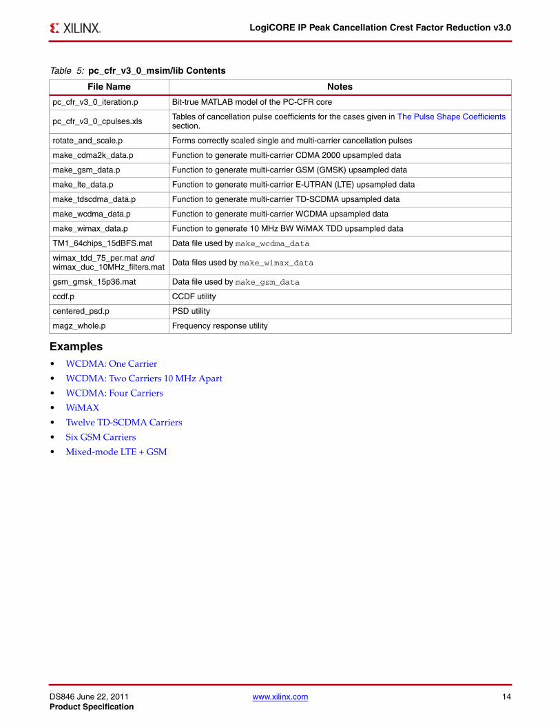
The file pc_cfr_v3_0_msim.zip can be obtained from the PC-CFR Evaluation Member Lounge (Registrationand Approval Required) and extracted. The functions require version R2009a or a compatible version. Theexamples require the Signal Processing Toolbox for the pulse design. If this is not available, the scripts should bemodified to use the supplied example pulses. The folder pc_cfr_v3_0_msim appears with a subfolder lib andfiles named and described in Table 4. The contents of the lib folder are named and described in Table 5. Theexamples can be run, modified as required, and used as templates for other applications and further investigations.b
Table 4: pc_cfr_v3_0 Contents
File Name Notes
examples_cdma2k.m Simulation of three adjacent CDMA 2000 carriers with fs = 30.72 Msps and PAR_target = 6 dB
examples_gsm6c_narrow.m Simulation of 6 GSM carriers spaced by 600 kHz with fs = 30.72 Msps and PAR_target = 5.5 dB
examples_gsm6c_wide.m Simulation of 6 GSM carriers spaced by 2 MHz with fs = 61.44 Msps and PAR_target = 5.5 dB
examples_lte1001.m Simulation of 2 x 5 MHz LTE carriers spaced 10 MHz apart with fs = 122.88 Msps and PAR_target swept from 5.5 to 8 dB in 0.5 dB steps
examples_lte20MHz.m Simulation of one 20 MHz LTE carrier with fs = 122.88 Msps and PAR_target = 7 dB
examples_lte40MHz.m Simulation of 2 x 20 MHz LTE carriers spaced 20 MHz apart with fs = 122.88 Msps and PAR_target = 7 dB
examples_mixed_mode.m Simulation of one 10 MHz LTE carrier mixed with 4 GSM carriers in a total of 20 MHz of spectrum with fs = 122.88 Msps and PAR_target = 6.5dB
examples_tds24c.m Simulation of twenty-four TD-SCDMA carriers spaced by 1.6 MHz with fs = 122.88 Msps and PAR_target = 7 dB
examples_tds12c.m Simulation of twelve TD-SCDMA carriers spaced by 1.6 MHz with fs = 61.44 Msps and PAR_target = 7 dB
examples_tds5c9.m Simulation of TD-SCDMA carriers occupying five of nine positions spaced by 1.6 MHz with fs = 92.16 Msps and PAR_target = 7 dB
examples_tds6c.m Simulation of six TD-SCDMA carriers spaced by 1.6 MHz with fs = 61.44 Msps and PAR_target = 7 dB
examples_wcdma1001.m Simulation of two WCDMA carriers spaced 10 MHz apart with fs = 122.88 Msps and PAR_target swept from 5.5 to 8 dB in 0.5 dB steps and data = Test Model 1 (TM1)
examples_wcdma1111.m Simulation of four adjacent WCDMA carriers with fs = 122.88 Msps and PAR_target = 6 dB and data = Test Model 1 (TM1)
examples_wcdma1c.m Simulation of one WCDMA carrier with fs = 30.72 Msps and PAR_target swept from 5.5 to 8 dB in 0.5 dB steps and data = Test Model 1 (TM1)
examples_wimax.m Simulation of a 10 MHz WiMAX TDD frame at fs = 61.44 Msps and PAR_target = 3.5dB in the preamble
DS846 June 22, 2011 www.xilinx.com 14Product Specification
LogiCORE IP Peak Cancellation Crest Factor Reduction v3.0
Examples• WCDMA: One Carrier
• WCDMA: Two Carriers 10 MHz Apart
• WCDMA: Four Carriers
• WiMAX
• Twelve TD-SCDMA Carriers
• Six GSM Carriers
• Mixed-mode LTE + GSM
Table 5: pc_cfr_v3_0_msim/lib Contents
File Name Notes
pc_cfr_v3_0_iteration.p Bit-true MATLAB model of the PC-CFR core
pc_cfr_v3_0_cpulses.xls Tables of cancellation pulse coefficients for the cases given in The Pulse Shape Coefficients section.
rotate_and_scale.p Forms correctly scaled single and multi-carrier cancellation pulses
make_cdma2k_data.p Function to generate multi-carrier CDMA 2000 upsampled data
make_gsm_data.p Function to generate multi-carrier GSM (GMSK) upsampled data
make_lte_data.p Function to generate multi-carrier E-UTRAN (LTE) upsampled data
make_tdscdma_data.p Function to generate multi-carrier TD-SCDMA upsampled data
make_wcdma_data.p Function to generate multi-carrier WCDMA upsampled data
make_wimax_data.p Function to generate 10 MHz BW WiMAX TDD upsampled data
TM1_64chips_15dBFS.mat Data file used by make_wcdma_data
wimax_tdd_75_per.mat and wimax_duc_10MHz_filters.mat Data files used by make_wimax_data
gsm_gmsk_15p36.mat Data file used by make_gsm_data
ccdf.p CCDF utility
centered_psd.p PSD utility
magz_whole.p Frequency response utility
DS846 June 22, 2011 www.xilinx.com 15Product Specification
LogiCORE IP Peak Cancellation Crest Factor Reduction v3.0
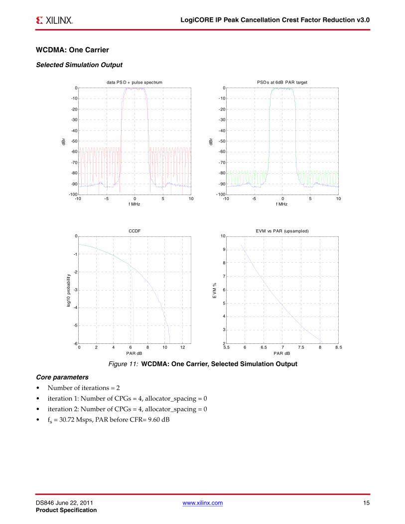
WCDMA: One Carrier
Selected Simulation Output
Core parameters
• Number of iterations = 2
• iteration 1: Number of CPGs = 4, allocator_spacing = 0
• iteration 2: Number of CPGs = 4, allocator_spacing = 0
• fs = 30.72 Msps, PAR before CFR= 9.60 dB
X-Ref Target - Figure 11
Figure 11: WCDMA: One Carrier, Selected Simulation Output
-10 -5 0 5 10-100
-90
-80
-70
-60
-50
-40
-30
-20
-10
0data PS D + pulse spectrum
f MHz
dBr
-10 -5 0 5 10-100
-90
-80
-70
-60
-50
-40
-30
-20
-10
0PSDs at 6dB PAR target
f MHz
dBr
0 2 4 6 8 10 12-6
-5
-4
-3
-2
-1
0CCDF
PAR dB
log1
0 pr
obab
ility
5.5 6 6.5 7 7.5 8 8. 52
3
4
5
6
7
8
9
10EVM vs PAR (upsampled)
PAR dB
EV
M %
DS846 June 22, 2011 www.xilinx.com 16Product Specification
LogiCORE IP Peak Cancellation Crest Factor Reduction v3.0
Discussion
The simulation produces the output shown along with additional graphical output (the signal magnitudes beforeand after each iteration) and test output (diagnostic information from each iteration).
The top left pane of Figure 11 plots the cancellation pulse shape (red) against the original spectrum, and the topright pane shows the signal spectrum before and after (green) CFR at the selected PAR_target stated. From theseplots it can be inferred that the equivalent clipping noise is around -20dBc as discussed previously.
The CCDF and PAR versus EVM plots are self-explanatory.
The text output shown gives the core physical parameters and in text form, the information given in the EVM andCCDF plots, and also three other key pieces of information:
1. The PAR at fs followed by the interpolated PAR. Here we see small differences that tell us that the fs chosen is sufficient for the signal bandwidth, and the signal can be safely interpolated after CFR.
2. The number of CPGs actually employed at each iteration. Four were provisioned (as stated in the General Considerations for Parameter Selection section) but, for example, if the application required only a 7dB PAR target, then this information says that the core need be configured for only three CPGs per iteration.
3. Less than 10% EVM can be achieved with PAR less than 6dB. The data in the first row of the simulator output table shows this, and also indicates that the CCDF is similar to that shown in the bottom hand pane of Figure 11.
Table 6: Results for WCDMA: One Carrier
PAR_target_dB PAR achieved at fs
PAR of interpolated
signal(245.76 Msps)
EVMCPGs used
at eachiteration
PAR at fsfor 10-1
prob
PAR at fsfor 10-2
prob
PAR at fsfor 10-3
prob
PAR at fsfor 10-4
prob
PAR at fsfor 10-5
prob
PAR at fsfor 10-6
prob
5.5 5.84 5.89 9.39 4, 3 3.77 5.73 5.82 5.84 5.87 5.91
6.0 6.25 6.29 7.47 4, 2 3.76 6.05 6.22 6.25 6.25 6.26
6.5 6.67 6.71 5.77 4, 2 3.74 6.34 6.65 6.67 6.68 6.68
7.0 7.11 7.15 4.30 3, 3 3.72 6.58 7.09 7.11 7.12 7.12
7.5 7.57 7.60 3.06 3, 2 3.71 6.72 7.55 7.57 7.58 7.59
8.0 8.03 8.07 2.05 2, 1 3.69 6.81 7.99 8.03 8.05 8.06
DS846 June 22, 2011 www.xilinx.com 17Product Specification
LogiCORE IP Peak Cancellation Crest Factor Reduction v3.0
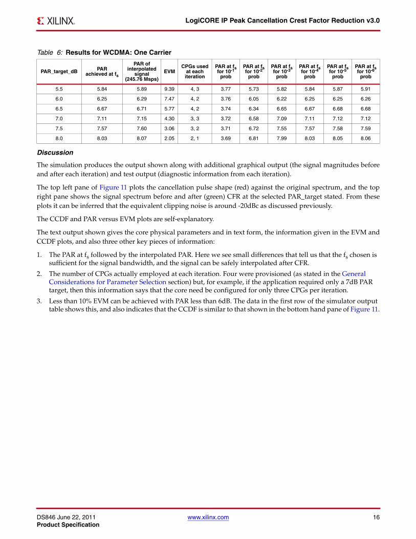
WCDMA: Two Carriers 10 MHz ApartSelected Simulation Output
Core parameters
• Number of iterations = 3
• iteration 1: Number of CPGs = 6, allocator_spacing = 20
• iteration 2: Number of CPGs = 6, allocator_spacing = 10
• iteration 3: Number of CPGs = 6, allocator_spacing = 5
• fs = 122.88 Msps, PAR before CFR= 9.88 dB
Discussion
The core parameters were selected to give good EVM and CCDF performance down to 6.5dB achieved PAR. Thereader can readily determine, by running the simulation with adjusted parameters, that the non-zero allocatorspacing values act to reduce the EVM, and that if the PAR requirements were higher, for example 7.5 dB, then onlytwo iterations would be required.
X-Ref Target - Figure 12
Figure 12: WCDMA: Two Carriers 10 MHz Apart, Selected Simulation Output
Table 7: Results for WCDMA: Two Carriers 10 MHz Apart
PAR_target_dB PAR achieved at fs
PAR of interpolatedsignal
(245.76 Msps)EVM
CPGs usedat eachiteration
PAR at fsfor 10-1
prob
PAR at fsfor 10-2
prob
PAR at fsfor 10-3
prob
PAR at fsfor 10-4
prob
PAR at fsfor 10-5
prob
PAR at fsfor 10-6
prob
5.5 6.02 6.13 12.32 6, 6, 6 3.69 5.73 5.99 6.02 6.07 6.42
6.0 6.38 6.49 9.95 6, 6, 6 3.70 5.97 6.35 6.38 6.41 6.69
6.5 6.76 6.88 7.85 6, 6, 3 3.70 6.19 6.74 6.76 6.79 7.01
7.0 7.17 7.28 6.03 6, 4, 3 3.69 6.38 7.15 7.17 7.19 7.23
7.5 7.60 7.70 4.49 5, 3, 2 3.68 6.54 7.59 7.60 7.62 7.63
8.0 8.06 8.12 3.22 4, 3, 2 3.67 6.66 7.93 8.06 8.08 8.09
-20 -10 0 10 20-100
-50
0data PSD + pulse spectrum
f MHz
dBr
-20 -10 0 10 20-100
-50
0PSDs at 6dB PAR target
f MHz
dB
r
0 5 10-6
-4
-2
0CCDF at 6dB PAR target
PAR dB
log1
0 p
roba
bili
ty
6 7 8 90
5
10
15EVM vs PAR (upsampled)
PAR dB
EV
M %
DS846 June 22, 2011 www.xilinx.com 18Product Specification
LogiCORE IP Peak Cancellation Crest Factor Reduction v3.0
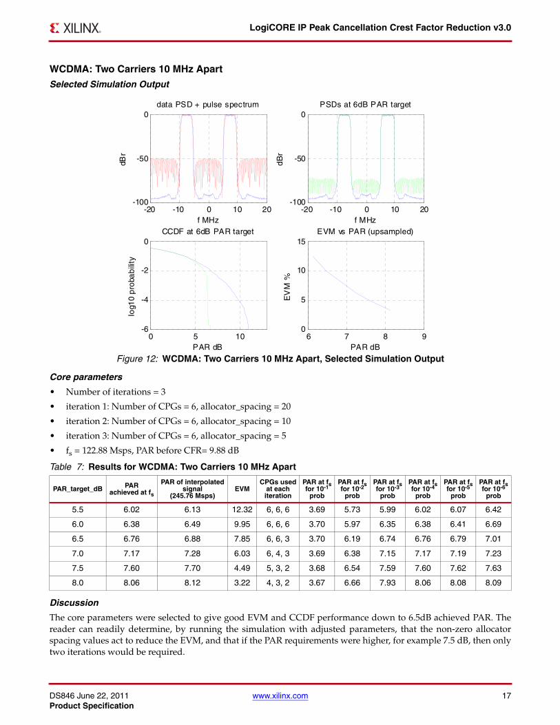
WCDMA: Four Carriers
Selected Simulation Output
Core parameters
• Number of iterations = 3
• iteration 1: Number of CPGs = 8, allocator_spacing = 0
• iteration 2: Number of CPGs = 8, allocator_spacing = 0
• iteration 3: Number of CPGs = 4, allocator_spacing = 0
• iteration 1: 6079 peaks out of 6175 were allocated max cpgs used = 8
• iteration 2: 835 peaks out of 835 were allocated max cpgs used = 8
• iteration 3: 135 peaks out of 135 were allocated max cpgs used = 4
• fs = 76.80 Msps, PAR before CFR = 12.41 dB
Discussion
This example operates on Test Model 3 (TM3) data, which is a more 'difficult' signal than TM1 used in the earlierWCDMA examples. In the single carrier case discussed earlier, the cancellation pulse is wider (in time) and henceneeds more taps for a proper filter realization (mitigating out-band leakage and in-band EVM). One straightforward way to cut down on number of taps is to reduce the sampling rate as the transmit signal bandwidth is less.In the contiguous multiple carrier case shown in the example here, a shorter pulse should be tried. In general, alonger cancellation pulse will block a CPG that much longer needing more CPGs per iteration for effectivecancellation. This effect is more prominent in the multiple carrier case where multiple peaks in close proximity aremore probable. Effective cancellation needs more CPGs in such cases and a relatively shorter pulse would yield a
X-Ref Target - Figure 13
Figure 13: WCDMA: Four Carriers, Selected Simulation Output
Table 8: Results for WCDMA: Four Carriers
PAR_target_dB PAR achieved at fs
PAR of interpolatedsignal
(245.76 Msps)EVM
CPGs usedat eachiteration
PAR at fsfor 10-1
prob
PAR at fsfor 10-2
prob
PAR at fsfor 10-3
prob
PAR at fsfor 10-4
prob
PAR at fsfor 10-5
prob
PAR at fsfor 10-6
prob
7.0 7.38 7.56 11.69 8, 8, 4 4.08 7.05 7.36 7.39 7.46 7.59
−20 −10 0 10 20−100
−90
−80
−70
−60
−50
−40
−30
−20
−10
0PSD before and after CFR
f MHz
dBr
0 2 4 6 8 10 12−6
−5
−4
−3
−2
−1
0CCDF
PAR dB
log1
0 pr
obab
ility
DS846 June 22, 2011 www.xilinx.com 19Product Specification
LogiCORE IP Peak Cancellation Crest Factor Reduction v3.0
better result. The four carrier example shown here needs more CPGs per iteration than a single carrier case as thereare more peaks to be cancelled (for the same PAR target), but a shorter pulse length helps in better utilization ofCPGs and cancelling all the peaks within three iterations. Note, the tap length has to be chosen judiciously to reduceleakage and EVM as well. Too relaxed (smaller value of tap length) a value will degrade leakage and EVM whereasa higher value (over-optimized) might lead to under-utilization of CPGs needing more iterations to cancel all thepeaks.
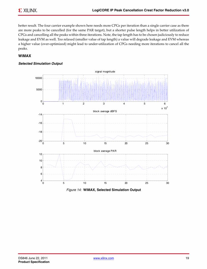
WiMAX
Selected Simulation Output X-Ref Target - Figure 14
Figure 14: WiMAX, Selected Simulation Output
0 1 2 3 4 5 6
x 104
0
5000
10000
signal magnitude
0 5 10 15 20 25 30-20
-18
-16
-14block average dBFS
0 5 10 15 20 25 304
6
8
10
12block average PAR

DS846 June 22, 2011 www.xilinx.com 20Product Specification
LogiCORE IP Peak Cancellation Crest Factor Reduction v3.0
Core parameters
• Number of iterations = 1
• iteration 1: Number of CPGs = 4, allocator_spacing = 0
• iteration 1: 350 peaks out of 350 were allocated max cpgs used = 3
• fs = 61.44 Msps, PAR before CFR= 4.32 dB
X-Ref Target - Figure 15
Figure 15: WiMAX, Entire Signal Amplitude before and after CFR
X-Ref Target - Figure 16
Figure 16: WiMAX, Spectra and CCDFs in the Preamble
Table 9: Results for WiMAX
PAR_target_dB PAR achieved at fs
PAR of interpolatedsignal
(245.76 Msps)EVM
CPGs usedat eachiteration
PAR at fsfor 10-1
prob
PAR at fsfor 10-2
prob
PAR at fsfor 10-3
prob
PAR at fsfor 10-4
prob
PAR at fsfor 10-5
prob
PAR at fsfor 10-6
prob
3.5 3.74 3.77 1.82 3 2.82 3.61 3.71 3.74 3.74 3.74
0 0.5 1 1.5 2 2.5 3 3.5
x 105
0
2000
4000
6000
8000
10000
12000iteration 1: Signal Amplitudes, PAR target(dB) = 3.50
-20 -15 -10 -5 0 5 10 15 20-100
-90
-80
-70
-60
-50
-40
-30
-20
-10
0PSD before and aft er CFR
f MHz
dBr
0 2 4 6 8 10 12-6
-5
-4
-3
-2
-1
0CCDF
PAR dB
log1
0 pr
obab
ility
DS846 June 22, 2011 www.xilinx.com 21Product Specification
LogiCORE IP Peak Cancellation Crest Factor Reduction v3.0
Discussion
The signal here is one in which there is a need to take into account that power (in some short-term average sense)is not constant across the frame. The signal here is a 75% downlink ratio signal in a typical maximum powerconfiguration.
The first plot of the simulation graphical output is the first millisecond of the 5mS frame and shows the mean powerand PAR in 4096 sample blocks. The preamble is the highest power, lowest PAR portion of the frame, and is scaledto -15dBFS. The full frame is at -20dBFS.
The objective of CFR is to limit the peak power for a given mean power, and the limiting factor in choosing thethreshold in this instance is the EVM budget. The ideal is to limit the peak power in the entire frame whilemaintaining about 2% EVM. It turns out that setting the PAR target to 3.5dB achieves this.
Figure 15 shows the entire signal amplitude before and after CFR, and Figure 16 shows the spectra and CCDFs inthe preamble. The corresponding numbers for the preamble appear in the text output. So the PAR of the preambleis reduced from 4.3 to 3.7, that is, only 0.7dB. But further analysis shows that the PAR of the entire frame (includingthe zero section) is reduced from 10.3 to 8.7. The message here is to set the threshold in relation to the maximumpower segment, and then the peak reduction of the entire frame follows.
Only one iteration is used in this simulation because the number of peaks that needs to be cancelled is relativelysmall. There is a residual time-domain ripple apparent in the preamble. If necessary, this can be removed with asecond iteration.
DS846 June 22, 2011 www.xilinx.com 22Product Specification
LogiCORE IP Peak Cancellation Crest Factor Reduction v3.0
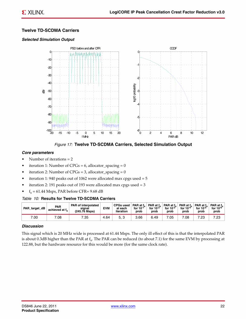
Twelve TD-SCDMA Carriers
Selected Simulation Output
Core parameters
• Number of iterations = 2
• iteration 1: Number of CPGs = 6, allocator_spacing = 0
• iteration 2: Number of CPGs = 3, allocator_spacing = 0
• iteration 1: 940 peaks out of 1062 were allocated max cpgs used = 5
• iteration 2: 191 peaks out of 193 were allocated max cpgs used = 3
• fs = 61.44 Msps, PAR before CFR= 9.68 dB
Discussion
This signal which is 20 MHz wide is processed at 61.44 Msps. The only ill effect of this is that the interpolated PARis about 0.3dB higher than the PAR at fs. The PAR can be reduced (to about 7.1) for the same EVM by processing at122.88, but the hardware resource for this would be more (for the same clock rate).
X-Ref Target - Figure 17
Figure 17: Twelve TD-SCDMA Carriers, Selected Simulation Output
Table 10: Results for Twelve TD-SCDMA Carriers
PAR_target_dB PAR achieved at fs
PAR of interpolatedsignal
(245.76 Msps)EVM
CPGs usedat eachiteration
PAR at fsfor 10-1
prob
PAR at fsfor 10-2
prob
PAR at fsfor 10-3
prob
PAR at fsfor 10-4
prob
PAR at fsfor 10-5
prob
PAR at fsfor 10-6
prob
7.00 7.08 7.35 4.64 5, 3 3.66 6.49 7.05 7.08 7.23 7.23
-20 -15 -10 -5 0 5 10 15 20-100
-90
-80
-70
-60
-50
-40
-30
-20
-10
0PSD before and after CFR
f MHz
dBr
0 2 4 6 8 10 12-6
-5
-4
-3
-2
-1
0CCDF
PAR dBlog
10 p
roba
bility

DS846 June 22, 2011 www.xilinx.com 23Product Specification
LogiCORE IP Peak Cancellation Crest Factor Reduction v3.0
Six GSM Carriers
Selected Simulation Output
Core parameters
• Number of iterations = 3
• iteration 1: Number of CPGs = 4, allocator_spacing = 160
• iteration 2: Number of CPGs = 4, allocator_spacing = 90
• iteration 3: Number of CPGs = 4, allocator_spacing = 0
• iteration 1: 962 peaks out of 4267 were allocated max cpgs used = 3
• iteration 2: 888 peaks out of 2050 were allocated max cpgs used = 4
• iteration 3: 242 peaks out of 245 were allocated max cpgs used = 4
• fs = 61.44 Msps, PAR before CFR= 7.97 dB
Discussion
The key point in this case is that GSM is a 'difficult signal' – the peaks are very dense because they are entirely dueto carrier mixing, as GMSK is a constant modulus signal. Therefore three iterations are used with carefully selectedallocator spacing values. Frequency-hopping GSM can be accommodated with dynamic cancellation pulseswitching as discussed in the Dynamic Cancellation Pulse Switching section.
X-Ref Target - Figure 18
Figure 18: Six GSM Carriers, Selected Simulation Output
Table 11: Results for Six GSM Carriers
PAR_target_dB PAR achieved at fs
PAR of interpolatedsignal
(245.76 Msps)EVM
CPGs usedat eachiteration
PAR at fsfor 10-1
prob
PAR at fsfor 10-2
prob
PAR at fsfor 10-3
prob
PAR at fsfor 10-4
prob
PAR at fsfor 10-5
prob
PAR at fsfor 10-6
prob
5.50 5.83 5.87 8.17 3, 4, 4 3.82 5.49 5.80 5.83 5.85 5.85
-20 -10 0 10 20-100
-90
-80
-70
-60
-50
-40
-30
-20
-10
0PSD before and after CFR
f MHz
dBr
0 2 4 6 8 10 12-6
-5
-4
-3
-2
-1
0CCDF
PAR dB
log
10 p
rob
abili
ty

DS846 June 22, 2011 www.xilinx.com 24Product Specification
LogiCORE IP Peak Cancellation Crest Factor Reduction v3.0
Mixed-mode LTE + GSM
Selected Simulation Output
Core parameters
• Number of iterations = 3
• iteration 1: Number of CPGs = 4, allocator_spacing = 150
• iteration 2: Number of CPGs = 4, allocator_spacing = 60
• iteration 3: Number of CPGs = 4, allocator_spacing = 0
• iteration 1: 2020 peaks out of 3193 were allocated max cpgs used = 4
• iteration 2: 926 peaks out of 1094 were allocated max cpgs used = 4
• iteration 3: 192 peaks out of 192 were allocated max cpgs used = 4
• fs = 122.88 Msps, PAR before CFR = 9.64 dB
Discussion
This example illustrates the application of the PC-CFR core to mixed-mode signals. Here, an LTE 10 MHz signal iscombined with a non-contiguous multi-carrier GSM signal. The two signals have been generated at different powerlevels and as a result, the individual cancellation pulses have been scaled by their relative power levels beforecombining to form the mixed-mode pulse. For more information on this scaling, refer to the MATLAB mixed-modeexample script provided. Here, a sample rate of 122.88 Msps has been chosen to achieve a PAR of 6.8 dB while stillmeeting the GSM spectral mask requirements.
X-Ref Target - Figure 19
Figure 19: Mixed-mode LTE + GSM, Selected Simulation Output
Table 12: Results for Mixed-mode LTE + GSM
PAR_target_dB PAR achieved at fs
PAR of interpolatedsignal
(245.76 Msps)EVM
CPGs usedat eachiteration
PAR at fsfor 10-1
prob
PAR at fsfor 10-2
prob
PAR at fsfor 10-3
prob
PAR at fsfor 10-4
prob
PAR at fsfor 10-5
prob
PAR at fsfor 10-6
prob
6.50 6.74 6.80 6.56 4, 4, 4 3.66 6.26 6.73 6.74 6.76 7.07
−20 −10 0 10 20−100
−90
−80
−70
−60
−50
−40
−30
−20
−10
0PSD before and after CFR
f MHz
dBr
0 2 4 6 8 10 12−6
−5
−4
−3
−2
−1
0CCDF
PAR dB
log1
0 pr
obab
ility
DS846 June 22, 2011 www.xilinx.com 25Product Specification
LogiCORE IP Peak Cancellation Crest Factor Reduction v3.0
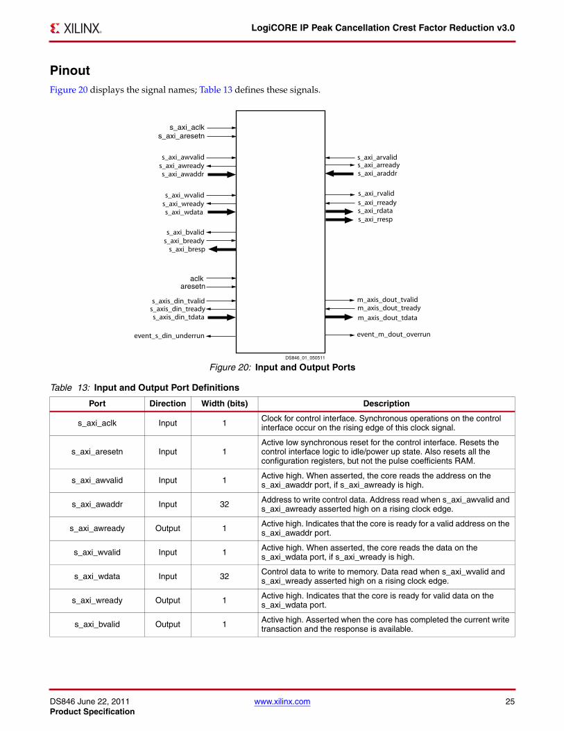
PinoutFigure 20 displays the signal names; Table 13 defines these signals.
X-Ref Target - Figure 20
Figure 20: Input and Output Ports
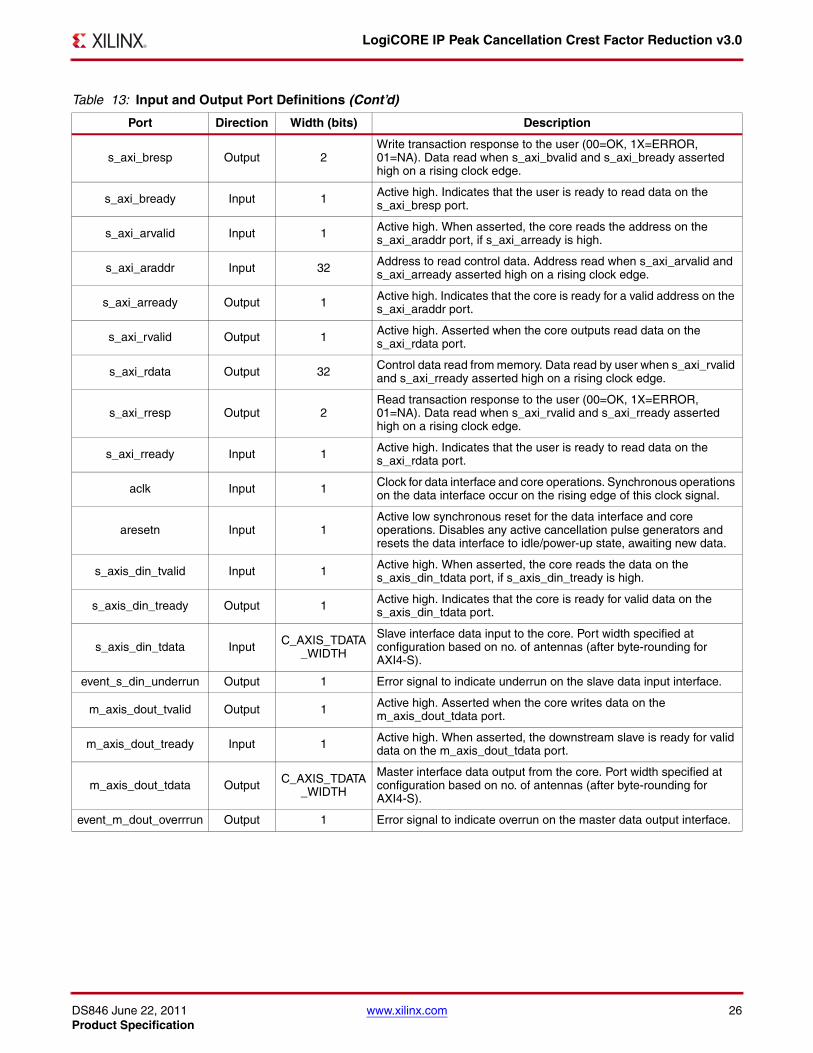
Table 13: Input and Output Port Definitions
Port Direction Width (bits) Description
s_axi_aclk Input 1 Clock for control interface. Synchronous operations on the control interface occur on the rising edge of this clock signal.
s_axi_aresetn Input 1Active low synchronous reset for the control interface. Resets the control interface logic to idle/power up state. Also resets all the configuration registers, but not the pulse coefficients RAM.
s_axi_awvalid Input 1 Active high. When asserted, the core reads the address on the s_axi_awaddr port, if s_axi_awready is high.
s_axi_awaddr Input 32 Address to write control data. Address read when s_axi_awvalid and s_axi_awready asserted high on a rising clock edge.
s_axi_awready Output 1 Active high. Indicates that the core is ready for a valid address on the s_axi_awaddr port.
s_axi_wvalid Input 1 Active high. When asserted, the core reads the data on the s_axi_wdata port, if s_axi_wready is high.
s_axi_wdata Input 32 Control data to write to memory. Data read when s_axi_wvalid and s_axi_wready asserted high on a rising clock edge.
s_axi_wready Output 1 Active high. Indicates that the core is ready for valid data on the s_axi_wdata port.
s_axi_bvalid Output 1 Active high. Asserted when the core has completed the current write transaction and the response is available.
s_axi_aclks_axi_aresetn
DS846_01_050511
s_axi_awvalid
s_axi_awaddrs_axi_awready
s_axi_wvalid
s_axi_wdatas_axi_wready
s_axi_bvalid
s_axi_bresps_axi_bready
aclkaresetn
s_axis_din_tvalid
s_axis_din_tdatas_axis_din_tready
event_s_din_underrun
s_axi_arvalid
s_axi_araddrs_axi_arready
s_axi_rvalid
s_axi_rdatas_axi_rready
event_m_dout_overrun
s_axi_rresp
m_axis_dout_tvalidm_axis_dout_treadym_axis_dout_tdata
DS846 June 22, 2011 www.xilinx.com 26Product Specification
LogiCORE IP Peak Cancellation Crest Factor Reduction v3.0
s_axi_bresp Output 2Write transaction response to the user (00=OK, 1X=ERROR, 01=NA). Data read when s_axi_bvalid and s_axi_bready asserted high on a rising clock edge.
s_axi_bready Input 1 Active high. Indicates that the user is ready to read data on the s_axi_bresp port.
s_axi_arvalid Input 1 Active high. When asserted, the core reads the address on the s_axi_araddr port, if s_axi_arready is high.
s_axi_araddr Input 32 Address to read control data. Address read when s_axi_arvalid and s_axi_arready asserted high on a rising clock edge.
s_axi_arready Output 1 Active high. Indicates that the core is ready for a valid address on the s_axi_araddr port.
s_axi_rvalid Output 1 Active high. Asserted when the core outputs read data on the s_axi_rdata port.
s_axi_rdata Output 32 Control data read from memory. Data read by user when s_axi_rvalid and s_axi_rready asserted high on a rising clock edge.
s_axi_rresp Output 2Read transaction response to the user (00=OK, 1X=ERROR, 01=NA). Data read when s_axi_rvalid and s_axi_rready asserted high on a rising clock edge.
s_axi_rready Input 1 Active high. Indicates that the user is ready to read data on the s_axi_rdata port.
aclk Input 1 Clock for data interface and core operations. Synchronous operations on the data interface occur on the rising edge of this clock signal.
aresetn Input 1Active low synchronous reset for the data interface and core operations. Disables any active cancellation pulse generators and resets the data interface to idle/power-up state, awaiting new data.
s_axis_din_tvalid Input 1 Active high. When asserted, the core reads the data on the s_axis_din_tdata port, if s_axis_din_tready is high.
s_axis_din_tready Output 1 Active high. Indicates that the core is ready for valid data on the s_axis_din_tdata port.
s_axis_din_tdata Input C_AXIS_TDATA_WIDTH
Slave interface data input to the core. Port width specified at configuration based on no. of antennas (after byte-rounding for AXI4-S).
event_s_din_underrun Output 1 Error signal to indicate underrun on the slave data input interface.
m_axis_dout_tvalid Output 1 Active high. Asserted when the core writes data on the m_axis_dout_tdata port.
m_axis_dout_tready Input 1 Active high. When asserted, the downstream slave is ready for valid data on the m_axis_dout_tdata port.
m_axis_dout_tdata Output C_AXIS_TDATA_WIDTH
Master interface data output from the core. Port width specified at configuration based on no. of antennas (after byte-rounding for AXI4-S).
event_m_dout_overrrun Output 1 Error signal to indicate overrun on the master data output interface.
Table 13: Input and Output Port Definitions (Cont’d)
Port Direction Width (bits) Description

DS846 June 22, 2011 www.xilinx.com 27Product Specification
LogiCORE IP Peak Cancellation Crest Factor Reduction v3.0
CORE Generator Software ParametersThe core configuration window is shown in Figure 21.
Component Name
The name of the core component to be instantiated. The name must begin with a letter and be composed of thefollowing characters: a to z, A to Z, 0 to 9, and '_'.
Configuration Settings
Data Rate (clock-cycles/sample)
This setting specifies the data-rate in clocks per sample where the core expects a new sample every n clock cyclesbased on the value specified. This enables the core to maximize resource savings based on the level of over-clocking.The available range is 1 to 4.
Datawidth
The datawidth must be in the range 11 to 18 bits. The width specified is used at the external interfaces, but allinternal values are represented by 18 bits. If a value less than 18 bits is specified, zero-padding on the LSB isperformed at the input interface and symmetric rounding is performed at the output interface. The threshold valueis also scaled up to 18 bits internally and need not be scaled by the user.
Number of Antennas
This setting specifies the number of antennas (transmit paths) required. The options available are 1, 2, 4 or 8. Thedata interface port width (C_AXIS_TDATA_WIDTH) scales with the number of antennas selected.
X-Ref Target - Figure 21
Figure 21: CORE Generator Configuration Window

DS846 June 22, 2011 www.xilinx.com 28Product Specification
LogiCORE IP Peak Cancellation Crest Factor Reduction v3.0
Number of Iterations
This setting specifies the number of iterations required. The available range is 1 to 8. The latency of the coreincreases with the number of iterations selected as given by Equation 1.
Number of Cancellation Pulse Generators per Iteration
This setting specifies the number of cancellation pulse generators available per iteration. The number specified isconfined to an integer multiple of the data-rate to maximize efficiency. The cancellation pulse generators can all beallocated independently and operate in parallel.
Max Cancellation Pulse Length
This setting specifies the maximum length of the cancellation pulse used. This is used to optimize block RAMutilization for storing the cancellation pulse coefficients. The available options are 511, 1023 and 2047.
Cancellation Pulse Length
This setting specifies the length of the cancellation pulse used. The available range is any odd value from 1 to MaxCancellation Pulse Length. This value is used for core latency calculation purpose only and the length of the actualcancellation pulse used could be different. In such a case, the core latency needs to be recalculated (based onEquation 1).
Latency
This setting specifies the desired latency of the core in number of samples. This is the latency from the first inputsample to the first output sample. The available range for this latency is given by Equation 1. This latencyparameter is actually used to define the max_peak_delay parameter. However, the first output valid has apre-defined latency from the first input valid which is given by Equation 2.
Equation 1
Equation 2
where Lcp is the cancellation pulse length, Timp is an implementation delay (see Table 14), Tmax_peak_delay is themax_peak_delay parameter (range: 32 to 200), Niter is the number of iterations and TAXI = 2 is a fixed delay in theAXI4-S slave and master interfaces.
Cancellation Pulse Coefficients Setup
Selecting configurable coefficients enables the pulse coefficients to be written and updated dynamically by aprocessor or other source. Selecting two pulses instead of a single pulse increases the coefficient memory required,but enables the user to update the pulse that is not in use and then dynamically switch to it after the update iscomplete.
Table 14: Implementation Delay
Data-rate Timp
1 40
2 34
3 32
4 32
Tdata Lcp 1–( ) 2⁄ Timp Tmax_peak_delay+ +( ) Niter× TAXI+=
Tvalid Niter TAXI+=
DS846 June 22, 2011 www.xilinx.com 29Product Specification
LogiCORE IP Peak Cancellation Crest Factor Reduction v3.0
When selecting fixed coefficients, a COE file is required. The coefficient values in the COE file must all be specifiedin radix 10 format as interleaved IQ values, that is, sample 1(I), sample 1(Q), sample 2(I), sample 2(Q) and so on. Formultiple antenna scenarios, the coefficients of the first antenna must come first, followed by the coefficients of thesecond antenna, and so on. The number of coefficients per antenna (assumed to be the same across all antennas) isinferred from the COE file and is reported in the core's configuration window. The number of coefficients perantenna must always be an odd value in the range 1 to Max Cancellation Pulse Length; each I (or Q) value must bewithin the range represented by a 16-bit signed number, that is, -32768 to 32767 inclusive. An example of a COE file:
radix=10;coefdata= 1, -1,-1, 1,1, -1;
Using the PC-CFR IP CoreThe CORE Generator™ GUI performs error-checking on all input parameters.
Several files are produced when a core is generated, and customized instantiation templates for Verilog and VHDLdesign flows are provided in the .veo and .vho files, respectively. For detailed instructions, see the CORE Generatorsoftware documentation.
Simulation Models
The PC-CFR core has a number of options for simulation models:
• VHDL behavioral model in the xilinxcorelib library
• VHDL UNISIM structural model
• Verilog UNISIM structural model
The models required can be selected in the CORE Generator tool project options.
Xilinx recommends that simulations utilizing UNISIM-based structural models are run using a resolution of 1 ps.Some Xilinx library components require a 1 ps resolution to work properly in either functional or timing simulation.The UNISIM-based structural models might produce incorrect results if simulation with a resolution other than 1ps. See the “Register Transfer Level (RTL) Simulation Using Xilinx Libraries” section in Synthesis and SimulationDesign Guide for more information. This document is part of the ISE® Software Manuals set available atwww.xilinx.com/support/documentation/dt_ise.htm.
XCO Parameters
Table 15 defines valid entries for the XCO parameters. Parameters are not case sensitive. Default values are dis-played in bold.
Xilinx strongly suggests that XCO parameters are not manually edited in the XCO file; instead, use the CORE Gen-erator GUI to configure the core and perform range and parameter value checking.
Table 15: XCO Parameters
XCO Parameter Valid Values
component_name ASCII text using characters: a to z, A to Z, 0 to 9 and '_' ; starting with a letter
data_rate 1 to 4
datawidth 11 to 18 (default value is 16)
c_num_antennas 1, 2, 4, 8

DS846 June 22, 2011 www.xilinx.com 30Product Specification
LogiCORE IP Peak Cancellation Crest Factor Reduction v3.0
Bit Accurate C Model
The Xilinx LogiCORE™ IP PC-CFR v3.0 core bit accurate C model is a self-contained, linkable, shared library thatmodels the functionality of this core with finite precision arithmetic. This model provides a bit accuraterepresentation of the various modes of the PC-CFR core, and it is suitable for inclusion in a larger framework forsystem-level simulation or core-specific verification.
The model is bit-accurate but not cycle-accurate; it performs exactly the same operations as the modes in the core.However, it does not model the core's latency or its interface signals. For further details, see the PC-CFR v3.0 BitAccurate C Model User Guide (UG808).
Demonstration Test Bench
When the core is generated using CORE Generator, a demonstration test bench is created. This is a simple VHDLtest bench that exercises the core. The demonstration test bench source code is one VHDL file:demo_tb/tb_<component_name>.vhd in the CORE Generator output directory. The source code iscomprehensively commented.
Using the Demonstration Test Bench
The demonstration test bench instantiates the generated PC-CFR core. If the CORE Generator project options are setto generate a structural model, a VHDL or Verilog netlist named <component_name>.vhd or<component_name>.v is generated. If this file is not present, generate it using the netgen program, for example:
netgen -sim -ofmt vhdl <component_name>.ngc <component_name>.vhd
Compile the netlist and the demonstration test bench into the work library (see your simulator documentation formore information on how to do this). Then simulate the demonstration test bench. View the test bench signals inyour simulator's waveform viewer to see the operations of the test bench.
c_num_iterations 1 to 8
cancellation_pulse_generator0 1 to 8, multiples of data_rate only (default value is 4)
cancellation_pulse_generator1 1 to 8, multiples of data_rate only (default value is 4)
cancellation_pulse_generator2 1 to 8, multiples of data_rate only (default value is 4)
cancellation_pulse_generator3 1 to 8, multiples of data_rate only (default value is 4)
cancellation_pulse_generator4 1 to 8, multiples of data_rate only (default value is 4)
cancellation_pulse_generator5 1 to 8, multiples of data_rate only (default value is 4)
cancellation_pulse_generator6 1 to 8, multiples of data_rate only (default value is 4)
cancellation_pulse_generator7 1 to 8, multiples of data_rate only (default value is 4)
max_cancellation_pulse_length 511, 1023, 2047
cancellation_pulse_length 1 to max_cancellation_pulse_length, odd values only
latency Within range given by Equation 1 (default value is upper bound)
coefficient_selectionSingle_pulse_fixed_coefficients, Single_pulse_configurable_coefficients, Two_pulses_configurable_coefficients
coe_fileno_coe_file_loaded in Single_pulse_configurable_coefficients and Two_pulses_configurable_coefficients modes; <filename>.coe in Single_pulse_fixed_coefficients mode
Table 15: XCO Parameters (Cont’d)
XCO Parameter Valid Values

DS846 June 22, 2011 www.xilinx.com 31Product Specification
LogiCORE IP Peak Cancellation Crest Factor Reduction v3.0
The Demonstration Test Bench in Detail
The demonstration test bench performs the following tasks:
• Instantiates the core
• Generates the clock and reset signals
• Drives the core's input signals to demonstrate core features
• Control write/read via AXI4-Lite interface
• Data I/O via AXI4-Stream interface
• Checks the core's output data against a reference output for errors
More information on the demonstration test bench is available in the tb_readme.txt file that is generated as partof the CORE Generator output.
AXI4-Stream ConsiderationsThe conversion to AXI4-Stream interfaces brings standardization and enhances interoperability of Xilinx IPLogiCORE solutions. Other than general control signals such as aclk and aresetn, and the control interface which isimplemented as an AXI4-Lite interface, all data interface inputs and outputs to the PC-CFR core are conveyed viaAXI4-Stream channels. A channel consists of TVALID and TDATA always, plus several optional ports and fields. Inthe PC-CFR core, the only optional port supported is TREADY.
For further details on AXI4-Stream interfaces see [Ref 5]and [Ref 6].
Basic Handshake
Figure 22 shows the transfer of data in an AXI4-Stream channel. TVALID is driven by the source (master) side of thechannel and TREADY is driven by the receiver (slave). TVALID indicates that the value in the payload field,TDATA, is valid. TREADY indicates that the slave is ready to receive data. When both TVALID and TREADY aretrue in a cycle, a transfer occurs. The master and slave set TVALID and TREADY respectively for the next transferappropriately.
TDATA Packing
The TDATA field of the AXI4-Stream interface carries packed data. In complex data types, the real component is inthe least significant position and the imaginary component follows, each are atomic subfields. To easeinteroperability with byte-oriented protocols, each subfield within TDATA that could be used independently is firstextended to fit a bit field that is a multiple of 8 bits. For example, say the PC-CFR core is configured to have adatawidth of 11 bits. Each of the real and imaginary components of the data is 11 bits wide. The real componentwould occupy bits 10 down to 0. Bits 15 down to 11 would be ignored. Bits 26 down to 16 would hold the imaginary
X-Ref Target - Figure 22
Figure 22: Data Transfer in an AXI4-Stream Channel
ACLK
ARESETN
TVALID
TREADY
TDATA D0 D1 D2
DS846 June 22, 2011 www.xilinx.com 32Product Specification
LogiCORE IP Peak Cancellation Crest Factor Reduction v3.0
component and bits 31 down to 27 would also be ignored. Sub-field packing and byte-rounding are shown inFigure 23. The bits added by byte orientation are ignored by the core and do not result in additional resource use.
TDATA Structure for DIN and DOUT Channels
Input port DIN and output port DOUT carry packed and byte-rounded data in their respective TDATA fields.Multiple antenna support is implemented by expanding the bus width of TDATA and packing the multiple antennastreams as follows: The N parallel streams of data from N antennas are packed as antenna 1 data (LSW), antenna 2data, …, antenna N data (MSW).
Migrating to PC-CFR v3.0 from Earlier Versions
XCO Parameter Changes
The CORE Generator core update functionality can be used to update an existing XCO file from PC-CFR v2.0 tov3.0, but it should be noted that the update mechanism alone does not create a core compatible with v2.0. SeeInstructions for Minimum Change Migration. PC-CFR v3.0 has additional parameters for AXI4-Stream andAXI4-Lite support. Table 16 shows the changes to XCO parameters from version 2.0 to version 3.0.
X-Ref Target - Figure 23
Figure 23: TDATA Packing for DIN and DOUT Ports
Table 16: XCO Parameter Changes from v2.0 to v3.0
Version v2.0 Version v3.0 Notes
component_name component_name Unchanged
data_rate data_rate Unchanged
datawidth datawidth Unchanged
c_num_antennas New to v3.0
c_num_iterations New to v3.0
cancellation_pulse_generator cancellation_pulse_generator0 Unchanged, but the parameter corresponds to the 1st iteration in v3.0, whereas there was only one iteration in v2.0
cancellation_pulse_generator1 New to v3.0
cancellation_pulse_generator2 New to v3.0
cancellation_pulse_generator3 New to v3.0
cancellation_pulse_generator4 New to v3.0
cancellation_pulse_generator5 New to v3.0
cancellation_pulse_generator6 New to v3.0
cancellation_pulse_generator7 New to v3.0
max_cancellation_pulse_length New to v3.0
cancellation_pulse_length New to v3.0
latency New to v3.0

DS846 June 22, 2011 www.xilinx.com 33Product Specification
LogiCORE IP Peak Cancellation Crest Factor Reduction v3.0
For more information on this upgrade feature, see the CORE Generator software documentation.
Port Changes
Table 17 details the changes to port naming, additional or deprecated ports and polarity changes from v2.0 to v3.0.
coefficient_selection coefficient_selection Unchanged
coe_file coe_file Unchanged
Table 17: Port Changes from v2.0 to v3.0
Version v2.0 Version v3.0 Notes
sreg_aclk s_axi_aclk Rename only
sreg_areset s_axi_aresetn Rename and polarity change (active high in v2.0; now active low).
sreg_awvalid s_axi_awvalid Write Address channel in AXI4-Lite slave interface (Write Address channel in Interface-X slave in v2.0).
sreg_awready s_axi_awready
sreg_awaddr s_axi_awaddr
sreg_wvalid s_axi_wvalid Write Data channel in AXI4-Lite slave interface (Write Data channel in Interface-X slave in v2.0).
sreg_wready s_axi_wready
sreg_wdata s_axi_wdata
s_axi_bvalid Write Response channel in AXI4-Lite slave interface.
s_axi_bready
s_axi_bresp
s_axi_arvalid Read Address channel in AXI4-Lite slave interface.
s_axi_arready
s_axi_araddr
s_axi_rvalid Read Data/Resp channel in AXI4-Lite slave interface.
s_axi_rready
s_axi_rdata
s_axi_rresp
sparam_threshold,sparam_alloc_spacing,sparam_filter_n_taps,sparam_filter_select
Configuration parameter interface in v2.0. Converted to memory mapped registers and accessed through AXI4-Lite interface in v3.0.
aclk aclk Unchanged.
areset aresetn Rename and polarity change (active high in v2.0; now active low).
sdata_valid s_axis_din_tvalid TVALID for AXI4-S slave interface (VALID for Interface-X slave in v2.0).
sdata_ready s_axis_din_tready TREADY for AXI4-S slave interface (READY for Interface-X slave in v2.0).
sdata_i s_axis_din_tdata Both sdata_i and sdata_q map to s_axis_din_tdata in v3.0.
sdata_q s_axis_din_tdata Both sdata_i and sdata_q map to s_axis_din_tdata in v3.0.
mdata_valid m_axis_dout_tvalid TVALID for AXI4-S master interface (VALID for Interface-X master in v2.0).
Table 16: XCO Parameter Changes from v2.0 to v3.0 (Cont’d)
Version v2.0 Version v3.0 Notes

DS846 June 22, 2011 www.xilinx.com 34Product Specification
LogiCORE IP Peak Cancellation Crest Factor Reduction v3.0
Latency Changes
The latency of PC-CFR v3.0 is different compared to v2.0 in general. The latency of v3.0 is user-selectable in a givenrange and can be obtained from Equation 1.
Instructions for Minimum Change Migration
To configure the PC-CFR v3.0 to most closely mimic the behavior of v2.0 the translation is as follows:
Parameters
Set
c_num_antennas to 1, c_num_iterations to 1, max_cancellation_pulse_length to 511, cancellation_pulse_length to 1 and latency to upper bound of the range specified in Equation 1;
cancellation_pulse_generator1 to cancellation_pulse_generator7 default to 4 and are unused.
All other parameters can be chosen as in v2.0.
Ports
Rename and map signals as detailed in Port Changes.
Performance
No change.
Resource Requirements and PerformanceThis section provides data on the resource requirements and performance for the core. Characterization has beendone on Virtex-7, Kintex-7, Virtex-6, and Spartan-6 FPGAs. Table 18 lists the devices used for characterization.
Resource requirements and performance are dependent mainly on the Data-Rate, Number of Cancellation PulseGenerators per Iteration, Number of Antennas, Number of Iterations and Max Cancellation Pulse Length. They arealso susceptible to the version of implementation tools used. Therefore, these example figures should be used as aguide only and verified before specific use. Maximum clock frequencies quoted do not take clock jitter into accountand should be derated by an amount appropriate to the clock source jitter specification.
mdata_ready m_axis_dout_tready TREADY for AXI4-S master interface (READY for Interface-X master in v2.0).
mdata_i m_axis_dout_tdata Both mdata_i and mdata_q map to m_axis_dout_tdata in v3.0.
mdata_q m_axis_dout_tdata Both mdata_i and mdata_q map to m_axis_dout_tdata in v3.0.
mstat_data[0] event_s_din_underrun Rename only.
mstat_data[1] event_m_dout_overrrun Rename only.
Table 18: Devices Used for Characterization
Virtex-7 Kintex-7 Virtex-6 Spartan-6
xc7v585t-1 xc7k325t-1 xc6vlx130t-1 xc6slx100-2
Table 17: Port Changes from v2.0 to v3.0 (Cont’d)
Version v2.0 Version v3.0 Notes
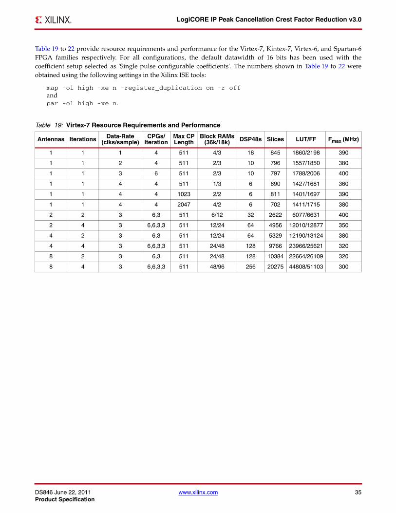
DS846 June 22, 2011 www.xilinx.com 35Product Specification
LogiCORE IP Peak Cancellation Crest Factor Reduction v3.0
Table 19 to 22 provide resource requirements and performance for the Virtex-7, Kintex-7, Virtex-6, and Spartan-6FPGA families respectively. For all configurations, the default datawidth of 16 bits has been used with thecoefficient setup selected as 'Single pulse configurable coefficients'. The numbers shown in Table 19 to 22 wereobtained using the following settings in the Xilinx ISE tools:
map -ol high -xe n -register_duplication on -r off andpar -ol high -xe n.
Table 19: Virtex-7 Resource Requirements and Performance
Antennas Iterations Data-Rate(clks/sample)
CPGs/Iteration
Max CPLength
Block RAMs(36k/18k) DSP48s Slices LUT/FF Fmax (MHz)
1 1 1 4 511 4/3 18 845 1860/2198 390
1 1 2 4 511 2/3 10 796 1557/1850 380
1 1 3 6 511 2/3 10 797 1788/2006 400
1 1 4 4 511 1/3 6 690 1427/1681 360
1 1 4 4 1023 2/2 6 811 1401/1697 390
1 1 4 4 2047 4/2 6 702 1411/1715 380
2 2 3 6,3 511 6/12 32 2622 6077/6631 400
2 4 3 6,6,3,3 511 12/24 64 4956 12010/12877 350
4 2 3 6,3 511 12/24 64 5329 12190/13124 380
4 4 3 6,6,3,3 511 24/48 128 9766 23966/25621 320
8 2 3 6,3 511 24/48 128 10384 22664/26109 320
8 4 3 6,6,3,3 511 48/96 256 20275 44808/51103 300

DS846 June 22, 2011 www.xilinx.com 36Product Specification
LogiCORE IP Peak Cancellation Crest Factor Reduction v3.0
Table 20: Kintex-7 Resource Requirements and Performance
Antennas Iterations Data-Rate(clks/sample)
CPGs/Iteration
Max CPLength
Block RAMs(36k/18k) DSP48s Slices LUT/FF Fmax (MHz)
1 1 1 4 511 4/3 18 843 1822/2198 350
1 1 2 4 511 2/3 10 734 1573/1850 370
1 1 3 6 511 2/3 10 920 1766/2006 380
1 1 4 4 511 1/3 6 691 1465/1681 390
1 1 4 4 1023 2/2 6 699 1420/1697 390
1 1 4 4 2047 4/2 6 698 1426/1715 390
2 2 3 6,3 511 6/12 32 2470 6128/6632 400
2 4 3 6,6,3,3 511 12/24 64 4651 12065/12877 370
4 2 3 6,3 511 12/24 64 4889 12293/13124 350
4 4 3 6,6,3,3 511 24/48 128 8054 24044/25621 370
8 2 3 6,3 511 24/48 128 9984 22702/26109 350
8 4 3 6,6,3,3 511 48/96 256 18793 44852/51103 310
Table 21: Virtex-6 Resource Requirements and Performance
Antennas Iterations Data-Rate(clks/sample)
CPGs/Iteration
Max CPLength
Block RAMs(36k/18k) DSP48s Slices LUT/FF Fmax (MHz)
1 1 1 4 511 4/3 18 802 1808/2189 400
1 1 2 4 511 2/3 10 704 1563/1825 400
1 1 3 6 511 2/3 10 857 1793/1965 400
1 1 4 4 511 1/3 6 634 1466/1649 400
1 1 4 4 1023 2/2 6 631 1398/1665 400
1 1 4 4 2047 4/2 6 683 1684/2171 400
2 2 3 6,3 511 6/12 32 2529 6098/6514 400
2 4 3 6,6,3,3 511 12/24 64 3935 12007/12636 350
4 2 3 6,3 511 12/24 64 4546 12171/12959 370
4 4 3 6,6,3,3 511 24/48 128 8928 24045/25198 360
8 2 3 6,3 511 24/48 128 9919 22655/25621 370
8 4 3 6,6,3,3 511 48/96 256 16445 45040/50110 330
Table 22: Spartan-6 Resource Requirements and Performance
Antennas Iterations Data-Rate(clks/sample)
CPGs/Iteration
Max CPLength
Block RAMs(18k/9k) DSP48s Slices LUT/FF Fmax (MHz)
1 1 1 4 511 6/1 18 783 1855/2247 250
1 1 2 4 511 4/1 10 709 1569/1900 250
1 1 3 6 511 4/1 10 782 1794/2042 250
1 1 4 4 511 3/1 6 710 1419/1721 250
1 1 4 4 1023 5/1 6 697 1426/1765 240
1 1 4 4 2047 9/1 6 728 1418/1780 230
2 2 1 4,4 511 24/4 72 2936 7223/8516 240
2 4 2 4,4,4,4 511 32/8 80 5070 11878/13707 200
4 2 2 4,4 511 32/8 80 6089 11005/14133 200
4 4 4 4,4,4,4 511 48/16 96 9838 19627/63288 200
DS846 June 22, 2011 www.xilinx.com 37Product Specification
LogiCORE IP Peak Cancellation Crest Factor Reduction v3.0
Glossary
References1. XAPP1128, Digital Predistortion v2.0
2. XAPP921, High Density WCDMA Digital Front End Reference Design
3. XAPP961, High Density WiMAX Digital Front End Reference Design
4. 3GPP Technical Specification GSM/EDGE, TS 45.005 V7.12.0 “Radio transmission and reception (Release 7)”
5. Xilinx AXI Design Reference Guide (UG761)
6. AMBA(r) 4 AXI4-Stream Protocol Version: 1.0 Specification.
7. UG808, LogiCORE IP Peak Cancellation Crest Factor Reduction v3.0 Bit Accurate C Model User Guide.
8. Peak Cancellation Crest Factor Reduction (PC-CFR) Product Page.
EvaluationAn evaluation license is available for this core. The evaluation version operates in the same way as the full versionfor several hours, dependant on clock frequency. Allocation of the cancellation pulse generators is then completelydisabled, and the data output comprises a delayed version of the data input. If you notice this behavior inhardware, it probably means you are using an evaluation version of the core. The Xilinx tools warn that anevaluation license is being used during netlist implementation. If a full license is installed, delete the old XCO file,reconfigure and regenerate the core.
Support Xilinx provides technical support at www.xilinx.com/support for this LogiCORE product when used as describedin the product documentation. Xilinx cannot guarantee timing, functionality, or support of product if implementedin devices that are not defined in the documentation, if customized beyond that allowed in the product documen-tation, or if changes are made to any section of the design labeled DO NOT MODIFY.
Acronym Definition
CFR Crest Factor Reduction
CPG Cancellation Pulse Generator
dBFSdB power relative to full scale. The (FDD) signals used in the simulation here are at -15dBFS within a 16 bit range, that is, the standard deviation is 32768*10-15/20 = 5827. For TDD signals, this applied to the maximum power segment.
DPD Digital Pre-Distortion
DUC Digital Up Converter
EVM
Error Vector Magnitude. The values reported here are obtained by comparing the total signals before and after CFR. Standards compliance measurement usually required this to be performed on demodulated baseband data. However good correlation is observed between the EVM values reported here and, for example, the values seen on the Agilent PSA for the WCDMA signals.
FDD Frequency Division Duplex. The inference here is that the signal frame has constant power within some timescale average.
PAR Peak to Average Ratio. The comparison between the peak signal amplitude that occurs with 10-4 probability and the mean. Also known as “Peak to Mean ratio” and PAPR (peak to average power ratio).
TDD Time Division Duplex. The signal frame is characterized by some blank periods and/or a non-uniform power profile.

DS846 June 22, 2011 www.xilinx.com 38Product Specification
LogiCORE IP Peak Cancellation Crest Factor Reduction v3.0
See the IP Release Notes Guide (XTP025) for further information on this core. There is a link to All DSP IP and then tothe relevant core.
For each core, there is a master Answer Record that contains the Release Notes and Known Issues list for the corebeing used. The following information is listed for each version of the core:
• New Features
• Bug Fixes
• Known Issues
Ordering Information
This Xilinx LogiCORE IP module is provided under the terms of the Xilinx Core Site License and the core is gener-ated using the Xilinx ISE CORE Generator software. The CORE Generator software is shipped with the Xilinx ISEDesign Suite software.
For full access to all core functionality in simulation and in hardware, you must purchase a license for the core. Con-tact your local Xilinx sales representative for information on pricing and availability of Xilinx LogiCORE IP mod-ules. Information about additional modules is also available at the Xilinx IP Center.
Revision HistoryThe following table shows the revision history for this document:
Notice of DisclaimerThe information disclosed to you hereunder (the “Materials”) is provided solely for the selection and use of Xilinx products. Tothe maximum extent permitted by applicable law: (1) Materials are made available “AS IS” and with all faults, Xilinx herebyDISCLAIMS ALL WARRANTIES AND CONDITIONS, EXPRESS, IMPLIED, OR STATUTORY, INCLUDING BUT NOTLIMITED TO WARRANTIES OF MERCHANTABILITY, NON-INFRINGEMENT, OR FITNESS FOR ANY PARTICULARPURPOSE; and (2) Xilinx shall not be liable (whether in contract or tort, including negligence, or under any other theory ofliability) for any loss or damage of any kind or nature related to, arising under, or in connection with, the Materials (includingyour use of the Materials), including for any direct, indirect, special, incidental, or consequential loss or damage (including lossof data, profits, goodwill, or any type of loss or damage suffered as a result of any action brought by a third party) even if suchdamage or loss was reasonably foreseeable or Xilinx had been advised of the possibility of the same. Xilinx assumes noobligation to correct any errors contained in the Materials or to notify you of updates to the Materials or to productspecifications. You may not reproduce, modify, distribute, or publicly display the Materials without prior written consent.Certain products are subject to the terms and conditions of the Limited Warranties which can be viewed athttp://www.xilinx.com/warranty.htm; IP cores may be subject to warranty and support terms contained in a license issued toyou by Xilinx. Xilinx products are not designed or intended to be fail-safe or for use in any application requiring fail-safeperformance; you assume sole risk and liability for use of Xilinx products in Critical Applications:http://www.xilinx.com/warranty.htm#critapps.
Date Version Description of Revisions
06/22/11 1.0 Initial Xilinx release. Previous version of this data sheet is DS750.