logic sniffer verilog fpga “demon core” advanced … · web viewthe following list documents...
TRANSCRIPT
Logic Sniffer Specification(Demon Core FPGA)
Version 1.03
Copyright © 2011-2012 Ian Davis
This document is free software; you can redistribute it and/or modify it under the terms of the GNU General Public License as published by the Free Software Foundation; either version 2 of
the License, or (at your option) any later version.
This document is distributed in the hope that it will be useful, but WITHOUT ANY WARRANTY; without even the implied warranty of MERCHANTABILITY or FITNESS FOR A PARTICULAR
PURPOSE. See the GNU General Public License for more details.
You should have received a copy of the GNU General Public License along with this document; if not, write to the Free Software Foundation, Inc., 51 Franklin St, Fifth Floor, Boston, MA 02110, USA

Logic Sniffer Demon Core FPGA Specification
Table of Contents
1 INTRODUCTION.......................................................................................................................41.1 ADVANCED TRIGGER.......................................................................................................5
2 BACKGROUND....................................................................................................................62.1 FPGA’S............................................................................................................................62.2 THE DATAPATH................................................................................................................72.3 THE SUMP PROTOCOL....................................................................................................8
2.3.1 Short Commands (one byte commands)..................................................................82.3.2 Long Commands (five byte commands)................................................................11
3 TRIGGER TERMS.............................................................................................................153.1 PROGRAMMING LOOKUP TABLES..................................................................................163.2 EXAMPLE (TRIGGER TERM INITIALIZATION).................................................................16
4 RANGE DETECTORS.......................................................................................................174.1 COMPLEX RANGE COMPARES........................................................................................184.2 PREPARE TARGET VALUES FOR COMPARATOR..............................................................184.3 RANGE COMPARE LUT CHAINS.....................................................................................184.4 EXAMPLE (RANGE DETECT INITIALIZATION).................................................................19
5 EDGE DETECTORS..........................................................................................................205.1 EXAMPLE (EDGE DETECTOR INITIALIZATION)...............................................................21
6 TIMERS................................................................................................................................226.1 EXAMPLE (TIMER INITIALIZATION)................................................................................22
7 TRIGGER SUMS................................................................................................................237.1 TRIGGER SUM INPUTS....................................................................................................237.2 TRIGGER SUM OPERATIONS...........................................................................................247.3 TRIGGER INVERTING......................................................................................................257.4 EXAMPLE (TRIGGER SUM INITIALIZATION)...................................................................26
8 TRIGGER SEQUENCE STATES.....................................................................................278.1 EXAMPLE (TRIGGER SEQUENCE INITIALIZATION)..........................................................28
APPENDIX A - ADVANCED TRIGGER CONFIG REGISTERS........................................29
APPENDIX B - EXAMPLE CODE...........................................................................................30
GNU GENERAL PUBLIC LICENSE..........................................................................................34
May 12, 2023 2 of 42 2:51 AM
Logic Sniffer Demon Core FPGA Specification
Table of Figures
Figure 1 - Block Diagram________________________________________________________________________4Figure 2 - Logic Block___________________________________________________________________________6Figure 3 - FPGA Layout_________________________________________________________________________6Figure 4 - AND gate equivalent____________________________________________________________________6Figure 5 - Datapath Diagram_____________________________________________________________________7Figure 6 - Basic Trigger Serial Mode______________________________________________________________14Figure 7 - Masked Compare_____________________________________________________________________15Figure 8 - Truth Table__________________________________________________________________________15Figure 9 - Trigger Term LUT____________________________________________________________________15Figure 10 - Initialize Trigger Term LUT Values______________________________________________________16Figure 11 - Carry Look Ahead Adder______________________________________________________________17Figure 12 - Carry Look Ahead Comparator_________________________________________________________17Figure 13 - Range LUT Organization______________________________________________________________18Figure 14 - Initialize Range Detector LUT Values____________________________________________________19Figure 15 - Edge Detector LUT___________________________________________________________________20Figure 16 - Initialize Edge Detector LUT Values_____________________________________________________21Figure 17 - Timer______________________________________________________________________________22Figure 18 - Initialize Timer Values________________________________________________________________22Figure 19 - Combination Trigger Sum_____________________________________________________________23Figure 20 - Pair LUT Operations_________________________________________________________________24Figure 21 - Mid LUT Operations__________________________________________________________________24Figure 22 - Final LUT Operations________________________________________________________________24Figure 23 - Initialize Trigger Sum_________________________________________________________________26Figure 24 - Example Sequence Level_______________________________________________________________27Figure 25 - Trigger Sequencer State Machine_______________________________________________________27Figure 26 - Initialize Trigger Sequence_____________________________________________________________28
Revision History
Feb 23, 2011 - Rev 1.01 - Initial Release.May 7, 2011 - Rev 1.02 - Clarified various points/problems (much thanks to flubberlab).Jan 1, 2012 - Rev 1.03 - Added section on implementing inverted trigger inputs.
May 12, 2023 3 of 42 2:51 AM
Logic Sniffer Demon Core FPGA Specification
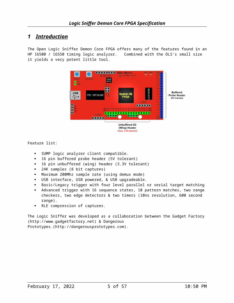
1 Introduction
The Open Logic Sniffer Demon Core FPGA offers many of the features found in an HP 16500 / 16550 timing logic analyzer. Combined with the OLS's small size it yields a very potent little tool.
Feature list:
SUMP logic analyzer client compatible. 16 pin buffered probe header (5V tolerant) 16 pin unbuffered (wing) header (3.3V tolerant) 24K samples (8 bit captures) Maximum 200Mhz sample rate (using demux mode) USB interface, USB powered, & USB upgradeable. Basic/Legacy trigger with four level parallel or serial target matching Advanced trigger with 16 sequence states, 10 pattern matches, two range checkers, two edge detectors &
two timers (10ns resolution, 600 second range). RLE compression of captures.
The Logic Sniffer was developed as a collaboration between the Gadget Factory (http://www.gadgetfactory.net) & Dangerous Prototypes.(http://dangerousprototypes.com).
Figure 1 - Block Diagram
May 12, 2023 4 of 42 2:51 AM
Logic Sniffer Demon Core FPGA Specification
1.1 Advanced Trigger
The advanced trigger offers many features found in an HP16500 / 16550 timing logic analyzer. It offers 16 sequence levels with two way branching (a programmable state machine), ten pattern value comparisons, two range checks, two edge checks, and two counter/timers.
There are several different modules within the advanced trigger, each needing its own spin on configuration. These are:
Trigger Terms. Terms perform the actual bitwise masked pattern comparisons on the 32-bit incoming data. There are ten terms. Each one needs 128 bits of configuration data.
Trigger Range Detectors. The two range detectors look for values falling between a lower & upper 32-bit limit. Each range check uses two 32-bit magnitude comparisons., one for the upper compare, one for the lower. A match means: “upper >= indata >= lower”. Each range detector needs 512 bits of configuration data.
Trigger Edge Detectors. The two edge detectors compare sampled input against a delayed version. Rising edges, falling edges, or both, or neither can thus be detected. Each needs 256 bits of configuration data.
Trigger Timers. Timers are started/stopped under control of the trigger sequence states. There are two timers, each needing a 36 bit limit value. The timers have a range from 10ns to over 11 minutes.
Trigger Sums. These combine the results of the trigger terms, range comparisons, edge checks, and timer checks. There are 11 logic units programmable to perform any logic function. Examples are AND/NAND/OR/NOR/XOR/NXOR. The logic units are combined in a tree structure, and combine/sum all trigger sources down to a match/miss signal. There are three trigger sums per trigger state, and 16 trigger states, totaling 48 sums. Each sum needs 192 bits of configuration data.
Trigger Sequence States. Each state is guided by the results of three trigger sums (see above). If the “hit” trigger sum matches, for a specified number of occurrences, the FSM advances. A hit also controls if a timer is started/stopped/cleared. If the “else” trigger sum matches, the FSM branches to the “else” state. Data capture is controlled by the “capture” trigger sum – if it matches, a sample is taken. If not, then not. Each state takes 32 bits of configuration.
Each module will be described in detail in the following chapters.
May 12, 2023 5 of 42 2:51 AM

Logic Sniffer Demon Core FPGA Specification
2 Background A little background to help put things in context...
2.1 FPGA’s
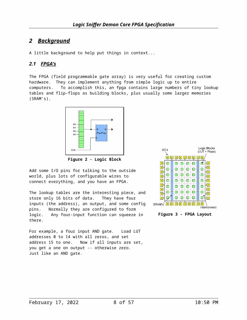
The FPGA (field programmable gate array) is very useful for creating custom hardware. They can implement anything from simple logic up to entire computers. To accomplish this, an fpga contains large numbers of tiny lookup tables and flip-flops as building blocks, plus usually some larger memories (SRAM’s).
Figure 2 - Logic Block
Figure 3 - FPGA Layout
Add some I/O pins for talking to the outside world, plus lots of configurable wires to connect everything, and you have an FPGA.
The lookup tables are the interesting piece, and store only 16 bits of data. They have four inputs (the address), an output, and some config pins. Normally they are configured to form logic. Any four-input function can squeeze in there.
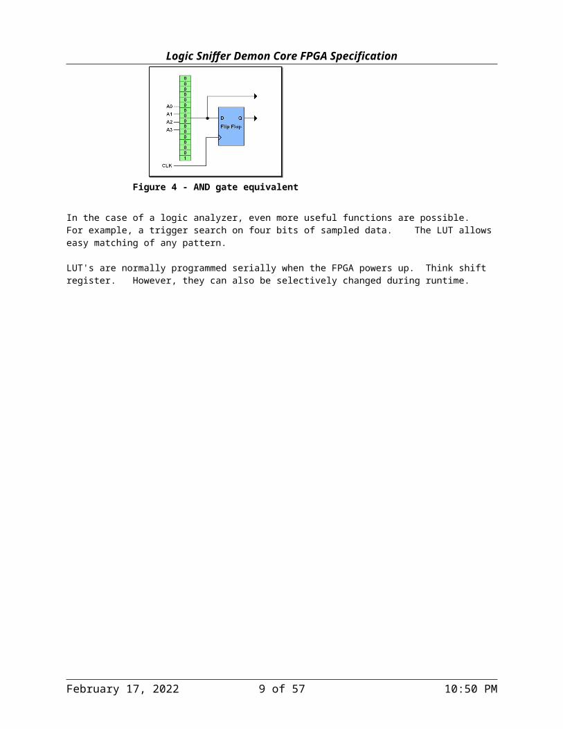
For example, a four input AND gate. Load LUT addresses 0 to 14 with all zeros, and set address 15 to one. Now if all inputs are set, you get a one on output -- otherwise zero. Just like an AND gate.
Figure 4 - AND gate equivalent
In the case of a logic analyzer, even more useful functions are possible. For example, a trigger search on four bits of sampled data. The LUT allows easy matching of any pattern.
LUT's are normally programmed serially when the FPGA powers up. Think shift register. However, they can also be selectively changed during runtime.
May 12, 2023 6 of 42 2:51 AM

Logic Sniffer Demon Core FPGA Specification
2.2 The Datapath
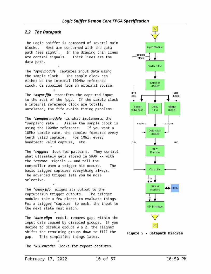
The Logic Sniffer is composed of several main blocks. Most are concerned with the data path (see right). In the drawing thin lines are control signals. Thick lines are the data path.
The “sync module” captures input data using the sample clock. The sample clock can either be the internal 100Mhz reference clock, or supplied from an external source.
The “async fifo” transfers the captured input to the rest of the fpga. If the sample clock & internal reference clock are totally unrelated, the fifo avoids timing problems.
The “sampler module” is what implements the “sampling rate”. Assume the sample clock is using the 100Mhz reference. If you want a 10Mhz sample rate, the sampler forwards every tenth valid capture. For 1Mhz, every hundredth valid capture, etc…
The “triggers” look for patterns. They control what ultimately gets stored in SRAM -- with the “capture” signals -- and tell the controller when a trigger hit occurs. The basic trigger captures everything always. The advanced trigger lets you be more selective.
The “delay fifo” aligns its output to the capture/run trigger outputs. The trigger modules take a few clocks to evaluate things. For a trigger “capture” to work, the input to the next state must match.
The “data align” module removes gaps within the input data caused by disabled groups. If you decide to disable groups 0 & 2, the aligner shifts the remaining groups down to fill the gap. This simplifies things later.
The “RLE encoder” looks for repeat captures. If found, counts are stored instead of repeats of unchanging data. This can greatly increase the effective storage capacity.
The “controller” is what decides how much gets captured, and when to send results to the client on your PC.
The “SRAM interface” handles saving & fetching captured data to & from the SRAM memory.
The “SPI interface” uploads the captures serially to the client. Only valid data is sent. Gaps due to disabled groups are filtered out.
A few remaining blocks aren’t shown here. The inbound SPI interface for receiving commands, the command decoder & flags register. Figure 5 - Datapath Diagram
May 12, 2023 7 of 42 2:51 AM
Logic Sniffer Demon Core FPGA Specification
2.3 The SUMP Protocol
The SUMP communication protocol assumes a standard RS232 port connection. Although the Logic Sniffer is USB based it emulates a very fast serial port from the perspective of the PC.
When sending captured data the analyzer sends back a contiguous block of data. Disabled channels are not sent however. First byte sent corresponds to sampled bits 7:0 (assuming channel 0 isn't disabled). The most recently captured data is returned first (ie: data is sent to client in reverse order). If Demux mode is enabled, group 2 and 3 inputs are ignored. Channel group 0 and 1 inputs are instead captured (if enabled) twice per sample - once each clock edge - and returned as a pair of bytes per group.
The following list documents the commands understood by the Logic Sniffer FPGA.
2.3.1 Short Commands (one byte commands)
0x00 - ResetReset the analyzer. Send at least five times to ensure FPGA in a known state. Clears any previous long commands that might have gotten stuck. The reset command should be issued prior to each Arm command (basic/legacy or advanced), to ensure previous captures/triggers are cleared.
0x01 - Arm Basic/Legacy TriggerArm the basic trigger. Sampling begins immediately. Once the trigger fires, the controller waits for "delay count" additional samples before returning captured data to client.
0x02 - Query IDThe device responds with four bytes. Currently "SLA1" to maintain backwards compatible SUMP protocol, output LSB first. ie: "1", "A", "L", "S"
May 12, 2023 8 of 42 2:51 AM
Logic Sniffer Demon Core FPGA Specification
0x04 - Query Meta DataThe device responds with a variable length block of data composed of one or more tokens + associated data.
Token 0 denotes end of meta data Tokens 0x01 to 0x1F are followed by a null terminated string (UTF-8 encoded). Tokens 0x20 to 0x3F are followed by a 32-bit unsigned integer (MSB first). Tokens 0x40 to 0x5F are followed by a 8-bit unsigned integer. All other token ranges are reserved.
The following fields are currently defined:
Token Description FPGA Currently Returns0x00 End of Meta Data 00x01 Device Name "Open Logic Sniffer v1.01"0x02 Version of FPGA firmware "3.0"0x03 Ancillary Version (PIC firmware) -0x20 Number of Probes -0x21 Sample memory available (bytes) 245760x22 Dynamic memory available (bytes) -0x23 Maximum sample rate (Hz) 2000000000x24 Protocol version -0x25 Capability Flags 0x0000001F0x40 Number of Probes (short version) 320x41 Protocol version (short version) 2
Clients should accept data from either long or short versions of a meta field, if both are possible.
The Capability Flags provide a bitmask indicating available FPGA features. Moving forward, this should help decouple the fpga from a needing a specific version of client (or visa versa).
Bit 0 - Basic Trigger available.Bit 1 - Advanced Trigger available.Bit 2 - RLE Encoding available (see flag register).Bit 3 - Extra RLE Encoding modes available (see flag register).Bit 4 - State capture mode available (see flag register)Bit 5 - Finish Now command available.Bit 6 - Query Input Data command available.Bit 7 - Query Capture State command available.Bit 8 - Return Capture Data command, and manual capture mode available (see flag register).Bits 31-9 - reserved
0x05 - Finish Now (disable RLE mode)Turns off RLE mode specified in the flags register (see 0x82 command below). In RLE mode, the analyzer can sit forever if inputs aren't changing. This gives the PC client application an opportunity to finish a capture on demand.
Finish now also aborts the advanced trigger, & forces data capture to quickly fill the buffer & end capture.
0x06 - Query Input DataThe device responds with four bytes. Gives a snapshot of the current logic analyzer input bits.
May 12, 2023 9 of 42 2:51 AM
Logic Sniffer Demon Core FPGA Specification
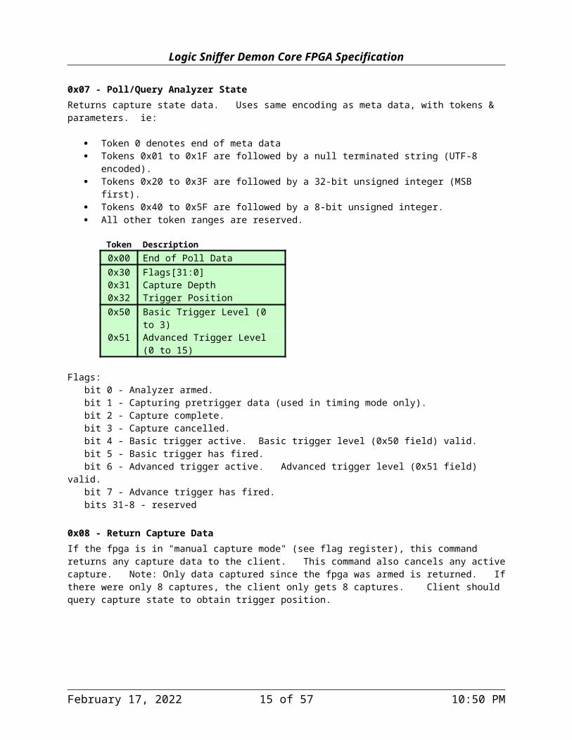
0x07 - Poll/Query Analyzer StateReturns capture state data. Uses same encoding as meta data, with tokens & parameters. ie:
Token 0 denotes end of meta data Tokens 0x01 to 0x1F are followed by a null terminated string (UTF-8 encoded). Tokens 0x20 to 0x3F are followed by a 32-bit unsigned integer (MSB first). Tokens 0x40 to 0x5F are followed by a 8-bit unsigned integer. All other token ranges are reserved.
Token Description0x00 End of Poll Data0x30 Flags[31:0]0x31 Capture Depth0x32 Trigger Position0x50 Basic Trigger Level (0 to 3)0x51 Advanced Trigger Level (0 to 15)
Flags: bit 0 - Analyzer armed. bit 1 - Capturing pretrigger data (used in timing mode only). bit 2 - Capture complete. bit 3 - Capture cancelled. bit 4 - Basic trigger active. Basic trigger level (0x50 field) valid. bit 5 - Basic trigger has fired. bit 6 - Advanced trigger active. Advanced trigger level (0x51 field) valid. bit 7 - Advance trigger has fired. bits 31-8 - reserved
0x08 - Return Capture DataIf the fpga is in "manual capture mode" (see flag register), this command returns any capture data to the client. This command also cancels any active capture. Note: Only data captured since the fpga was armed is returned. If there were only 8 captures, the client only gets 8 captures. Client should query capture state to obtain trigger position.
0x0F - Arm Advanced TriggerArm the advanced trigger. Conditional capturing (under control of trigger sequencer) begins immediately. Once trigger fires, the controller waits for "delay count" additional samples before returning captured data to client.
0x11 - XONDepreciated. On a serial port, this would pause output when FPGA was returning captured data. Currently ignored by the FPGA.
0x13 - XOFFDepreciated. On a serial port, this would resume output when FPGA was returning captured data. Currently ignored by the FPGA.
May 12, 2023 10 of 42 2:51 AM
Logic Sniffer Demon Core FPGA Specification
2.3.2 Long Commands (five byte commands)
0x80 - Set Sample RateThe Logic Sniffer samples at rates lower than the reference clock by using a divisor-count. Every given number of clocks, a sample is accepted. To set the sample rate, the divisor count is computed as follows:
divider = (clock / sample-rate) - 1
0x81 - Set Read Count & Delay CountThe read-count specifies the number of samples (divided by four) to be returned to the client on your PC. The delay-count is the number of samples (divided by four) to capture -after- the basic or advanced trigger fires. Samples are defined as one byte per each enabled input group.
A read-count larger than the delay-count returns captures from before the trigger. Such pre-trigger captures are only valid if the device was running long enough before the trigger fired. ie: a trigger that fires immediately could return garbage.
May 12, 2023 11 of 42 2:51 AM
Logic Sniffer Demon Core FPGA Specification
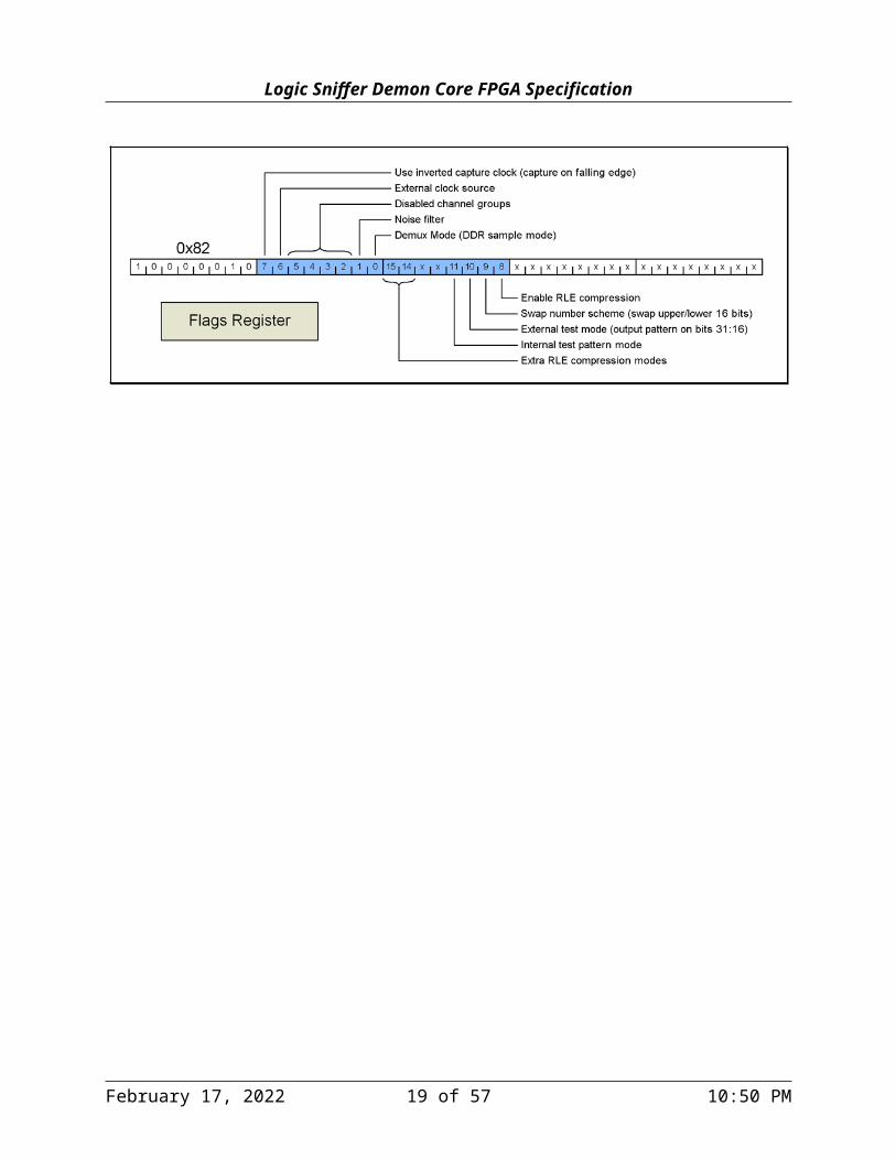
0x82 - Set FlagsThe flags register configures a whole range of miscellaneous Logic Sniffer features including:
Demux Mode. Double-Data-Rate Capturing. Captures groups 0 & 1 inputs on both edges of internal reference clock (ie: two samples per clock per enabled group). Not compatible with Noise Filter mode. Should only be used with max sample-rate (ie: set divisor to zero -- see 0x80 above). 1= Enabled.
Noise Filter Mode. Reduces occurrence of glitches on inputs. 1 = Enabled. Disabled Channel Groups. Don't capture specified groups of input data. Input channels 0-7, 8-15, 16-23,
and 24-31 correspond to Channel Groups 0, 1, 2, and 3 respectively. If Demux mode is enabled, then Group 2 and 3 settings must equal Group 0 and 1 settings. 1 = Disable group.
External Clock Source. Use external clock for sampling. If disabled, use internal 100Mhz reference clock instead. When enabled the Logic Sniffer is basically in "state mode" (sample synchronous with input) verses "timing mode" (asynchronous internal reference clock). 1 = Enabled.
Inverted External Capture Clock. Capture data on falling edge of sample clock when using external clock. Enable RLE compression mode. Duplicate samples are compressed into counts. Most significant bit of
sample replaced with "rle-flag", and is thus no longer available. Requires client support to decode. A value is stored, followed by a count of repeats. Count's are exclusive of value, so <value><count=7> means there are 8 samples.
Swap Number Scheme. Swap upper 16 bits & lower 16 bits of input in capture buffer. 1 = Enabled. External test mode. Output 16-bit test pattern on capture pins 31:16. 1 = Enabled. Internal test mode. Supply internally generated 32-bit test pattern to capture buffer. Input data is ignored. State capture mode. If 1, enables trigger sequencer controlled data capturing. Extra RLE compression modes. For input samples which change infrequently, rle-count's can fill to
maximum. The Logic Sniffer then stores that count & starts counting again. The extra modes control how often another <value> is stored (even if it hasn't changed):
Mode Description0&1 Issue <value> & <rle-count> as pairs. Backwards compatible.
2 Periodic. <values> reissued approximately every 256 <rle-count> fields. 3 Unlimited. <values> can be followed by unlimited numbers of <rle-counts>.
May 12, 2023 12 of 42 2:51 AM

Logic Sniffer Demon Core FPGA Specification
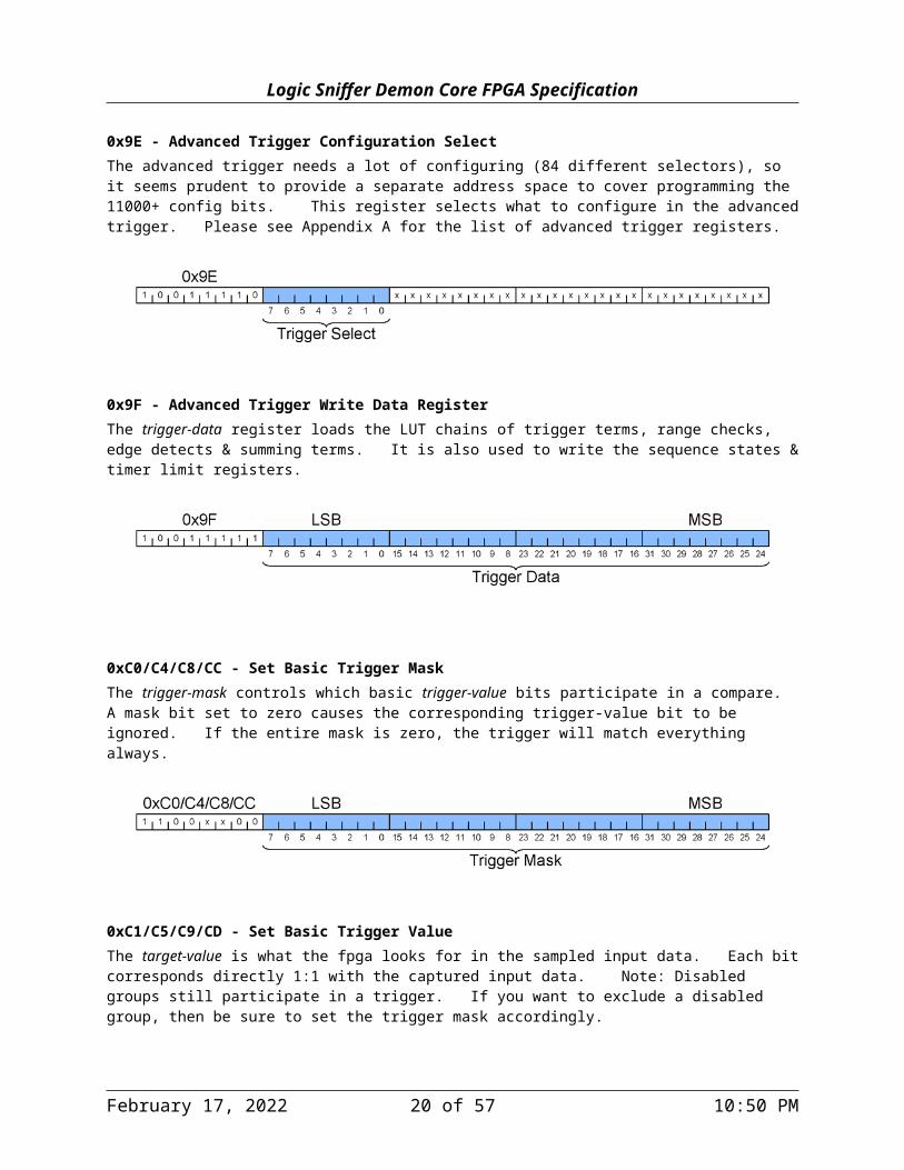
0x9E - Advanced Trigger Configuration SelectThe advanced trigger needs a lot of configuring (84 different selectors), so it seems prudent to provide a separate address space to cover programming the 11000+ config bits. This register selects what to configure in the advanced trigger. Please see Appendix A for the list of advanced trigger registers.
0x9F - Advanced Trigger Write Data RegisterThe trigger-data register loads the LUT chains of trigger terms, range checks, edge detects & summing terms. It is also used to write the sequence states & timer limit registers.
0xC0/C4/C8/CC - Set Basic Trigger MaskThe trigger-mask controls which basic trigger-value bits participate in a compare. A mask bit set to zero causes the corresponding trigger-value bit to be ignored. If the entire mask is zero, the trigger will match everything always.
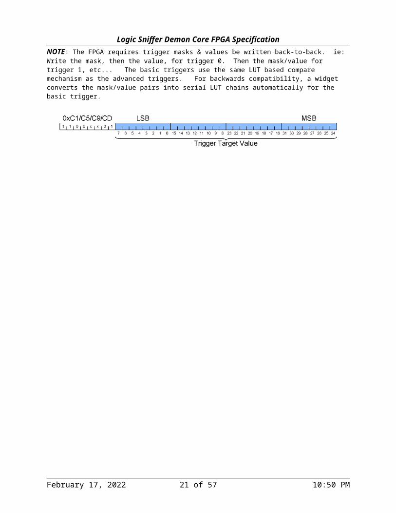
0xC1/C5/C9/CD - Set Basic Trigger ValueThe target-value is what the fpga looks for in the sampled input data. Each bit corresponds directly 1:1 with the captured input data. Note: Disabled groups still participate in a trigger. If you want to exclude a disabled group, then be sure to set the trigger mask accordingly.
NOTE: The FPGA requires trigger masks & values be written back-to-back. ie: Write the mask, then the value, for trigger 0. Then the mask/value for trigger 1, etc... The basic triggers use the same LUT based compare mechanism as the advanced triggers. For backwards compatibility, a widget converts the mask/value pairs into serial LUT chains automatically for the basic trigger.
May 12, 2023 13 of 42 2:51 AM
Logic Sniffer Demon Core FPGA Specification
0xC2/C6/CA/CE - Set Basic Trigger ConfigurationWriting this register configures the selected basic trigger stage. There are various fields available for customizing the operation of the trigger:
Stage Delay. If a trigger match occurs, the action of the stage is delayed by number of samples. Serial Mode. If enabled, trigger operates as a serial trigger. 1 = Serial Mode. Serial Channel. In serial mode, select which input pin to treat as serial channel (0 to 31). Level. Trigger level at which current stage will become active. Level 0 means activate immediately. Start. Tell controller the basic trigger has fired.
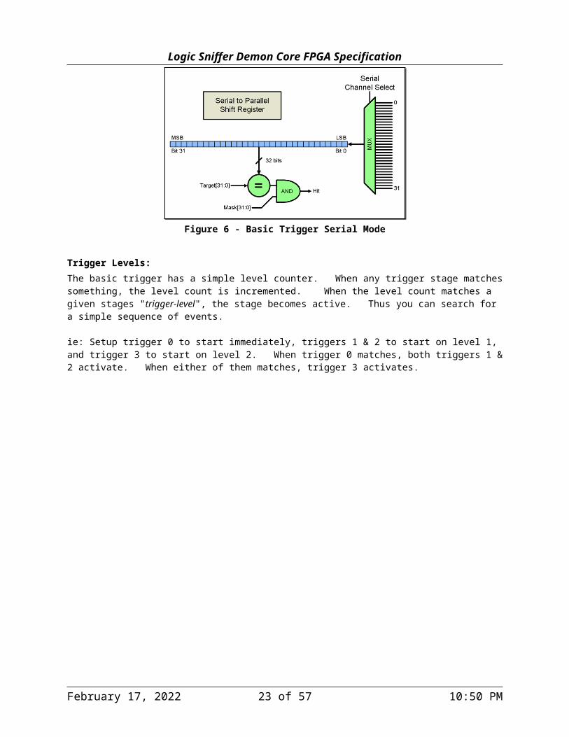
Serial Mode:In serial mode, a basic triggers stage monitors only a single sampled input bit, selected with the "serial-channel". The selected bit is fed into a serial-to-parallel shift register. Thus the last 32 samples of a single bit can be evaluated using the normal masked compare logic.
To be effective, you should use an external clock in serial mode. Otherwise it's very difficult to predict exactly when samples are taken & added to the shift register. So for example, when monitoring a SPI bus use the SPI clock for capturing.
Figure 6 - Basic Trigger Serial Mode
Trigger Levels:The basic trigger has a simple level counter. When any trigger stage matches something, the level count is incremented. When the level count matches a given stages "trigger-level", the stage becomes active. Thus you can search for a simple sequence of events.
ie: Setup trigger 0 to start immediately, triggers 1 & 2 to start on level 1, and trigger 3 to start on level 2. When trigger 0 matches, both triggers 1 & 2 activate. When either of them matches, trigger 3 activates.
May 12, 2023 14 of 42 2:51 AM
Logic Sniffer Demon Core FPGA Specification
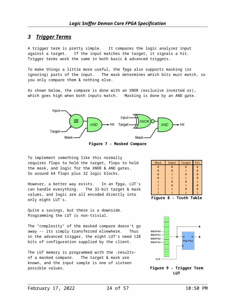
3 Trigger Terms A trigger term is pretty simple. It compares the logic analyzer input against a target. If the input matches the target, it signals a hit. Trigger terms work the same in both basic & advanced triggers.
To make things a little more useful, the fpga also supports masking (or ignoring) parts of the input. The mask determines which bits must match, so you only compare them & nothing else.
As shown below, the compare is done with an XNOR (exclusive inverted or), which goes high when both inputs match. Masking is done by an AND gate.
Figure 7 - Masked Compare
To implement something like this normally requires flops to hold the target, flops to hold the mask, and logic for the XNOR & AND gates. So around 64 flops plus 32 logic blocks.
However, a better way exists. In an fpga, LUT's can handle everything. The 32-bit target & mask values, and logic are all encoded directly into only eight LUT's.
Quite a savings, but there is a downside. Programming the LUT is non-trivial.
The "complexity" of the masked compare doesn't go away -- its simply transferred elsewhere. Thus in the advanced trigger, the eight LUT's need 128 bits of configuration supplied by the client.
The LUT memory is programmed with the -results- of a masked compare. The target & mask are known, and the input sample is one of sixteen possible values.
Thus we simply run through all combinations in advance. ie:
LUT address 0 stores result of: (0 ^ value) & mask)==0LUT address 1 stores result of: (1 ^ value) & mask)==0LUT address 2 stores result of: (2 ^ value) & mask)==0LUT address 3 stores result of: (3 ^ value) & mask)==0LUT address 4 stores result of: (4 ^ value) & mask)==0etc…
Figure 8 - Truth Table
Figure 9 - Trigger Term LUT
For each of the eight LUT's, the above is repeated with different 4 bit chunks of value & mask.
May 12, 2023 15 of 42 2:51 AM
Mask Input Target Hit0 0 0 00 0 1 00 1 0 00 1 1 01 0 0 11 0 1 01 1 0 01 1 1 1

Logic Sniffer Demon Core FPGA Specification
3.1 Programming Lookup Tables
To enable easier LUT programming, the fpga contains a built in parallel-to-serial converter. You simply write a long SUMP command to the chain address. Note the SUMP protocol dictates the least significant data byte be output first.
Once the fpga receives the long command, the bytes are organized MSB first (bits 31 downto 0), and then serially shifted into the LUT chain.
Some of the advanced trigger modules are quite complex and need multiple writes to fully load their LUT chains. Chains vary in length up to 512 bits.
3.2 Example (Trigger Term Initialization)
#define write_select(value) write_long_command (0x9E, value)#define write_chain(value) write_long_command (0x9F, value)
void write_term (int term_number, unsigned int target, unsigned int mask){ unsigned int bitmask=1; unsigned int lutvalue0=0; unsigned int lutvalue1=0; unsigned int lutvalue2=0; unsigned int lutvalue3=0;
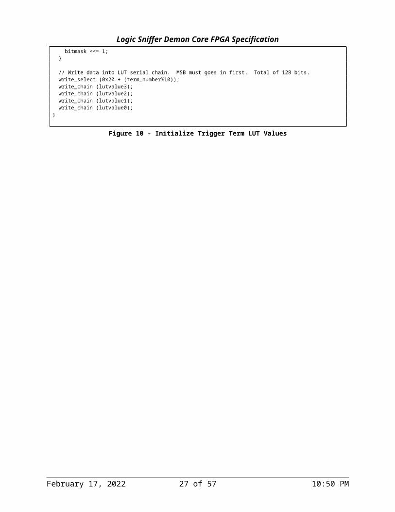
for (int i=0; i<16; i=i+1) { if (((i ^ (target & 0xF)) & (mask & 0xF))==0) lutvalue0 |= bitmask; if (((i ^ ((target>>4) & 0xF)) & ((mask>>4) & 0xF))==0) lutvalue0 |= (bitmask<<16); if (((i ^ ((target>>8) & 0xF)) & ((mask>>8) & 0xF))==0) lutvalue1 |= bitmask; if (((i ^ ((target>>12) & 0xF)) & ((mask>>12) & 0xF))==0) lutvalue1 |= (bitmask<<16); if (((i ^ ((target>>16) & 0xF)) & ((mask>>16) & 0xF))==0) lutvalue2 |= bitmask; if (((i ^ ((target>>20) & 0xF)) & ((mask>>20) & 0xF))==0) lutvalue2 |= (bitmask<<16); if (((i ^ ((target>>24) & 0xF)) & ((mask>>24) & 0xF))==0) lutvalue3 |= bitmask; if (((i ^ ((target>>28) & 0xF)) & ((mask>>28) & 0xF))==0) lutvalue3 |= (bitmask<<16); bitmask <<= 1; }
// Write data into LUT serial chain. MSB must goes in first. Total of 128 bits. write_select (0x20 + (term_number%10)); write_chain (lutvalue3); write_chain (lutvalue2); write_chain (lutvalue1); write_chain (lutvalue0);
May 12, 2023 16 of 42 2:51 AM

Logic Sniffer Demon Core FPGA Specification}
Figure 10 - Initialize Trigger Term LUT Values
May 12, 2023 17 of 42 2:51 AM
Logic Sniffer Demon Core FPGA Specification
4 Range Detectors The advanced trigger supports detecting when sampled data falls within a range of values. ie: if the sample is between a lower limit & upper limit. ie:
hit = (upper-limit >= sample) && (sample >= lower-limit)
So we need magnitude comparators. In hardware, that means adding or subtracting two numbers to see if something overflows or "carry's" over. A bit like long addition. Add a column, carry the one, add another, etc...
In hardware there is parallel to long addition: the full adder. The adder adds A+B+Cin, and outputs S & Cout, where all signals are single bits. To add wide values you chain the carry signals as needed.
Chains of full adders work, but are slow. The carry-out signal is derived from the inputs. In a 32-bit adder, there would be 32 chained carry circuits. Achieving timing would be harder than necessary.
An improvement is the carry-look-ahead adder. There is still a combinatorial element per bit, but it's very fast -- a simple mux. The fpga even has an integral "fast-carry-chain" circuit available for implementing such adders.
Figure 11 - Carry Look Ahead Adder
To make things even better, a magnitude comparison doesn't need the sum output at all. Just the fast carry chain. Thus we end up with something that fits perfectly into a single Logic Block. The LUT table simply needs loading with the result of an XOR between the input on A0, and the target value.
=>
Figure 12 - Carry Look Ahead Comparator
May 12, 2023 18 of 42 2:51 AM
A B CIn Cout S0 0 0 0 00 0 1 0 10 1 0 0 10 1 1 1 01 0 0 0 11 0 1 1 01 1 0 1 01 1 1 1 1
Truth Table for Full Adder
Logic Sniffer Demon Core FPGA Specification
4.1 Complex Range Compares
The fast carry change logic has a couple of interesting possibilities.
First of all, the range comparison can start anywhere. If the first bit of interest is bit 7 (for example), simply fill all lower LUT's with 1's. This NOP's them in the comparator.
Second, the bits participating in the range comparison don't need to be contiguous. You could setup to range check the value formed by indata bits 7,9,11, & 15. Simply NOP the LUT's of the don't care indata bits.
4.2 Prepare Target Values for Comparator
There are two ways to compare a value. Subtract a value & look for underflow/borrow, or add & look for overflow/carry. Since we have the fast-carry-chain, we're using the latter approach.
A given range target must be bitwise inverted before being programmed. For non-contiguous range checks, the inverted value must also be spaced out, across only those bits of interest.
Lower value = ~(lower_target - 1)Upper value = ~(upper_target)
Yields a hit if (upper_target >= indata >= lower_target)
4.3 Range Compare LUT Chains
There are 32 LUT's in each range-check magnitude comparator. Each needs 16-bits, so that totals 512 bits of configuration. Two LUT's are programmed at once for each write to the chain-data register.
Figure 13 - Range LUT Organization
May 12, 2023 19 of 42 2:51 AM
Logic Sniffer Demon Core FPGA Specification
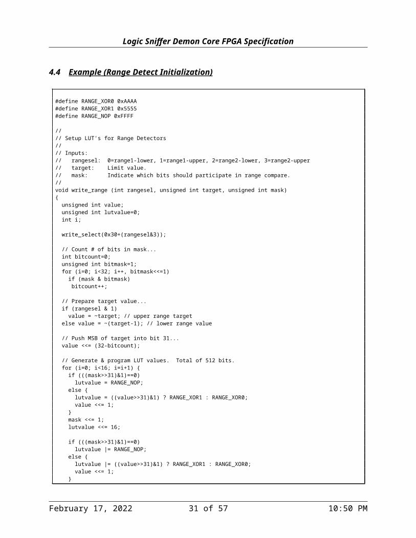
4.4 Example (Range Detect Initialization)
#define RANGE_XOR0 0xAAAA#define RANGE_XOR1 0x5555#define RANGE_NOP 0xFFFF
//// Setup LUT's for Range Detectors//// Inputs:// rangesel: 0=range1-lower, 1=range1-upper, 2=range2-lower, 3=range2-upper// target: Limit value.// mask: Indicate which bits should participate in range compare. //void write_range (int rangesel, unsigned int target, unsigned int mask){ unsigned int value; unsigned int lutvalue=0; int i;
write_select(0x30+(rangesel&3));
// Count # of bits in mask... int bitcount=0; unsigned int bitmask=1; for (i=0; i<32; i++, bitmask<<=1) if (mask & bitmask) bitcount++;
// Prepare target value... if (rangesel & 1) value = ~target; // upper range target else value = ~(target-1); // lower range value
// Push MSB of target into bit 31... value <<= (32-bitcount);
// Generate & program LUT values. Total of 512 bits. for (i=0; i<16; i=i+1) { if (((mask>>31)&1)==0) lutvalue = RANGE_NOP; else { lutvalue = ((value>>31)&1) ? RANGE_XOR1 : RANGE_XOR0; value <<= 1; } mask <<= 1; lutvalue <<= 16;
if (((mask>>31)&1)==0) lutvalue |= RANGE_NOP; else { lutvalue |= ((value>>31)&1) ? RANGE_XOR1 : RANGE_XOR0; value <<= 1; } mask <<= 1;
write_chain(lutvalue); }}
Figure 14 - Initialize Range Detector LUT Values
May 12, 2023 20 of 42 2:51 AM
Logic Sniffer Demon Core FPGA Specification
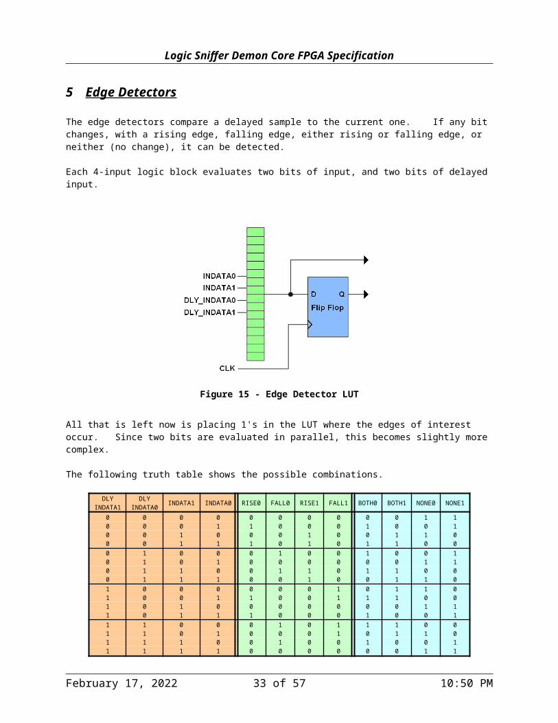
5 Edge Detectors
The edge detectors compare a delayed sample to the current one. If any bit changes, with a rising edge, falling edge, either rising or falling edge, or neither (no change), it can be detected.
Each 4-input logic block evaluates two bits of input, and two bits of delayed input.
Figure 15 - Edge Detector LUT
All that is left now is placing 1's in the LUT where the edges of interest occur. Since two bits are evaluated in parallel, this becomes slightly more complex.
The following truth table shows the possible combinations.
DLYINDATA
1
DLYINDATA
0INDATA
1INDATA
0 RISE0 FALL0 RISE1 FALL1 BOTH0
BOTH1
NONE0
NONE1
0 0 0 0 0 0 0 0 0 0 1 10 0 0 1 1 0 0 0 1 0 0 10 0 1 0 0 0 1 0 0 1 1 00 0 1 1 1 0 1 0 1 1 0 00 1 0 0 0 1 0 0 1 0 0 10 1 0 1 0 0 0 0 0 0 1 10 1 1 0 0 1 1 0 1 1 0 00 1 1 1 0 0 1 0 0 1 1 01 0 0 0 0 0 0 1 0 1 1 01 0 0 1 1 0 0 1 1 1 0 01 0 1 0 0 0 0 0 0 0 1 11 0 1 1 1 0 0 0 1 0 0 11 1 0 0 0 1 0 1 1 1 0 01 1 0 1 0 0 0 1 0 1 1 01 1 1 0 0 1 0 0 1 0 0 11 1 1 1 0 0 0 0 0 0 1 1
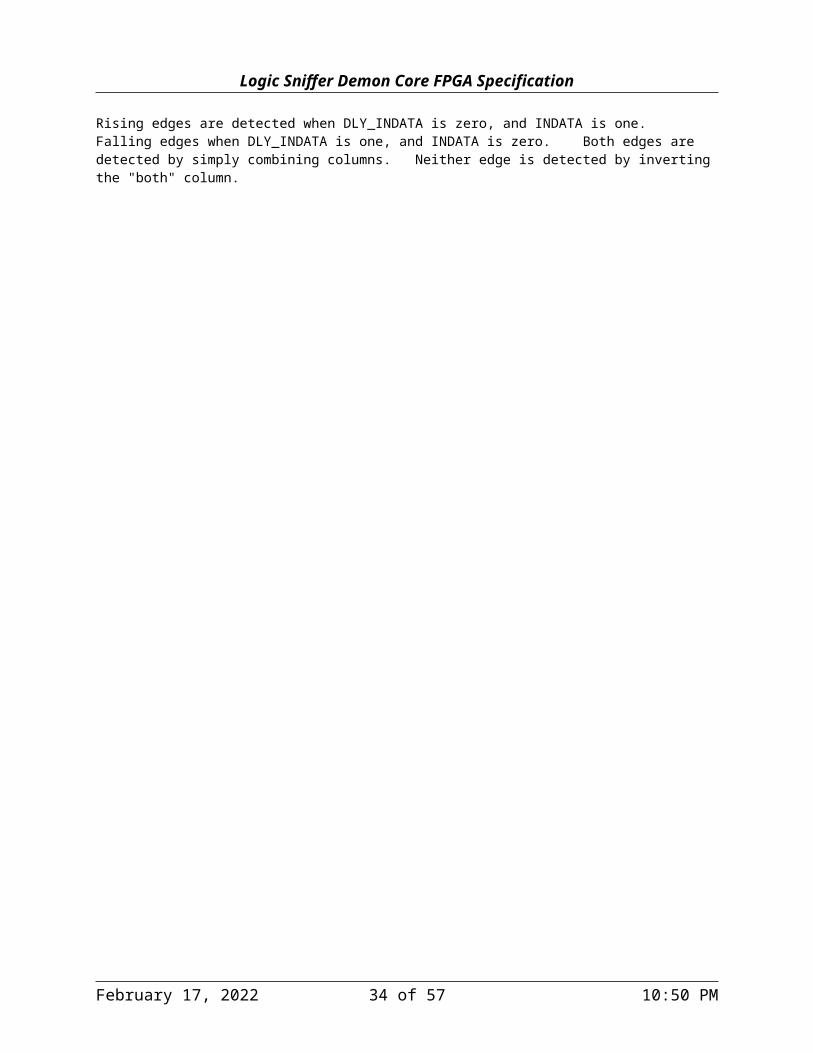
Rising edges are detected when DLY_INDATA is zero, and INDATA is one. Falling edges when DLY_INDATA is one, and INDATA is zero. Both edges are detected by simply combining columns. Neither edge is detected by inverting the "both" column.
May 12, 2023 21 of 42 2:51 AM

Logic Sniffer Demon Core FPGA Specification
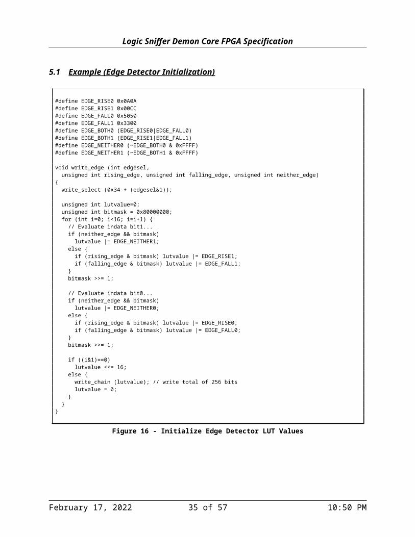
5.1 Example (Edge Detector Initialization)
#define EDGE_RISE0 0x0A0A#define EDGE_RISE1 0x00CC#define EDGE_FALL0 0x5050#define EDGE_FALL1 0x3300#define EDGE_BOTH0 (EDGE_RISE0|EDGE_FALL0)#define EDGE_BOTH1 (EDGE_RISE1|EDGE_FALL1)#define EDGE_NEITHER0 (~EDGE_BOTH0 & 0xFFFF)#define EDGE_NEITHER1 (~EDGE_BOTH1 & 0xFFFF)
void write_edge (int edgesel, unsigned int rising_edge, unsigned int falling_edge, unsigned int neither_edge){ write_select (0x34 + (edgesel&1));
unsigned int lutvalue=0; unsigned int bitmask = 0x80000000; for (int i=0; i<16; i=i+1) { // Evaluate indata bit1... if (neither_edge && bitmask) lutvalue |= EDGE_NEITHER1; else { if (rising_edge & bitmask) lutvalue |= EDGE_RISE1; if (falling_edge & bitmask) lutvalue |= EDGE_FALL1; } bitmask >>= 1;
// Evaluate indata bit0... if (neither_edge && bitmask) lutvalue |= EDGE_NEITHER0; else { if (rising_edge & bitmask) lutvalue |= EDGE_RISE0; if (falling_edge & bitmask) lutvalue |= EDGE_FALL0; } bitmask >>= 1;
if ((i&1)==0) lutvalue <<= 16; else { write_chain (lutvalue); // write total of 256 bits lutvalue = 0; } }}
Figure 16 - Initialize Edge Detector LUT Values
May 12, 2023 22 of 42 2:51 AM
Logic Sniffer Demon Core FPGA Specification
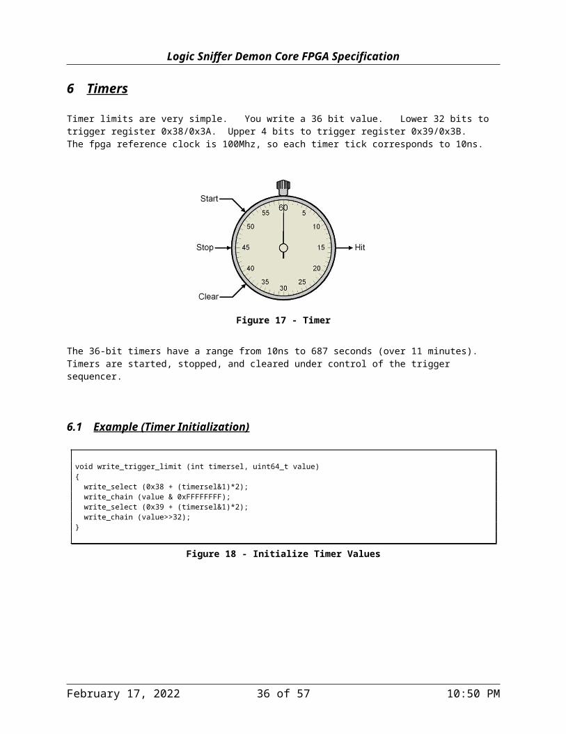
6 Timers
Timer limits are very simple. You write a 36 bit value. Lower 32 bits to trigger register 0x38/0x3A. Upper 4 bits to trigger register 0x39/0x3B. The fpga reference clock is 100Mhz, so each timer tick corresponds to 10ns.
Figure 17 - Timer
The 36-bit timers have a range from 10ns to 687 seconds (over 11 minutes). Timers are started, stopped, and cleared under control of the trigger sequencer.
6.1 Example (Timer Initialization)
void write_trigger_limit (int timersel, uint64_t value){ write_select (0x38 + (timersel&1)*2); write_chain (value & 0xFFFFFFFF); write_select (0x39 + (timersel&1)*2); write_chain (value>>32);}
Figure 18 - Initialize Timer Values
May 12, 2023 23 of 42 2:51 AM
Logic Sniffer Demon Core FPGA Specification
7 Trigger Sums The trigger summing logic combines the results of the trigger terms, range detectors, edge detectors and timers.
Figure 19 - Combination Trigger Sum
Each of the operations (the "OR" blocks shown above) are implemented using LUT memories. Therefore, they can be configured with any logical operation. Typical functions are: AND, NAND, OR, NOR, XOR, NXOR, A-only, B-only, ANY, or NOP.
In addition, the LUT memories can be used to invert the result of a trigger term, range, edge or timer detect (anything in the first column above). For example, allowing "a" or "not a", or "in_range" or "out of range" variations, etc...
There are three trigger sums per sequencer state, and sixteen trigger sequencer states, for a total of 48 trigger sums which need configuring.
7.1 Trigger Sum Inputs
As mentioned earlier, the inputs to the sum are trigger terms, range detectors, edge detectors and timers. Results of all inputs feed into the "pair" LUT's (which evaluate a pair of sum inputs each).
Trigger Terms. 32-bit masked compares. Each term supplies a two bit result. LSB corresponds to indata[15:0]. MSB to indata[31:16]. Both bits must be asserted to indicate a hit.
Range Detectors. The range detectors similarly supply two signals. LSB is the lower limit hit. MSB is upper limit hit. Both bits must be asserted to indicate a hit.
Edge Detectors. Single hit/miss signal. Fed into both bits 2 & 3 of pair LUT.
Timer. Single hit/miss signal. Fed into both bits 2 & 3 of pair LUT.
May 12, 2023 24 of 42 2:51 AM

Logic Sniffer Demon Core FPGA Specification
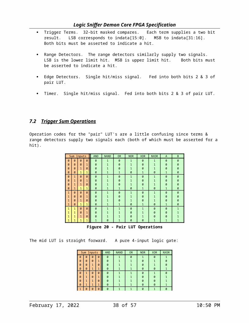
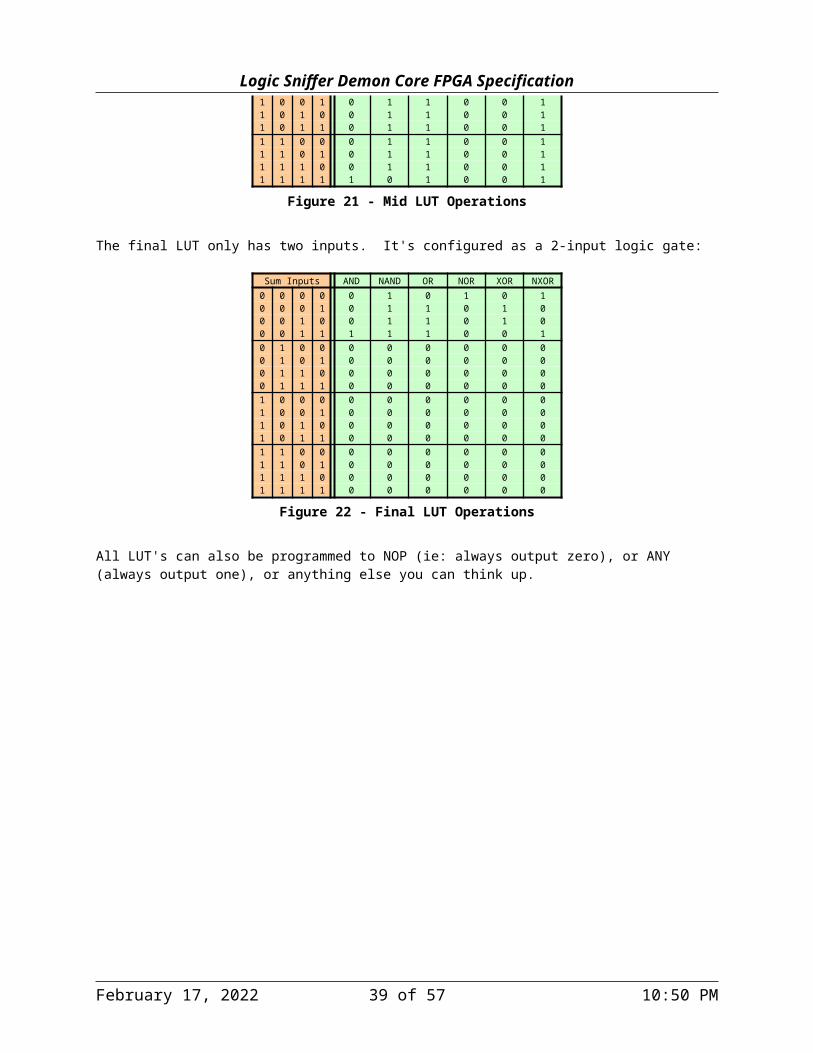
7.2 Trigger Sum Operations
Operation codes for the "pair" LUT's are a little confusing since terms & range detectors supply two signals each (both of which must be asserted for a hit).
Sum Inputs AND NAND OR NOR XOR NXO
RA B
0 0 0 0 0 1 0 1 0 1 0 00 0 0 1 0 1 0 1 0 1 0 00 0 1 0 0 1 0 1 0 1 0 00 0 1 1 0 1 1 0 1 0 1 00 1 0 0 0 1 0 1 0 1 0 00 1 0 1 0 1 0 1 0 1 0 00 1 1 0 0 1 0 1 0 1 0 00 1 1 1 0 1 1 0 1 0 1 01 0 0 0 0 1 0 1 0 1 0 01 0 0 1 0 1 0 1 0 1 0 01 0 1 0 0 1 0 1 0 1 0 01 0 1 1 0 1 1 0 1 0 1 01 1 0 0 0 1 1 0 1 0 0 11 1 0 1 0 1 1 0 1 0 0 11 1 1 0 0 1 1 0 1 0 0 11 1 1 1 1 0 1 0 0 1 1 1
Figure 20 - Pair LUT Operations
The mid LUT is straight forward. A pure 4-input logic gate:
Sum Inputs AND NAND OR NOR XOR NXO
R0 0 0 0 0 1 0 1 0 10 0 0 1 0 1 1 0 1 00 0 1 0 0 1 1 0 1 00 0 1 1 0 1 1 0 0 10 1 0 0 0 1 1 0 1 00 1 0 1 0 1 1 0 0 10 1 1 0 0 1 1 0 0 10 1 1 1 0 1 1 0 0 11 0 0 0 0 1 1 0 1 01 0 0 1 0 1 1 0 0 11 0 1 0 0 1 1 0 0 11 0 1 1 0 1 1 0 0 11 1 0 0 0 1 1 0 0 11 1 0 1 0 1 1 0 0 11 1 1 0 0 1 1 0 0 11 1 1 1 1 0 1 0 0 1
Figure 21 - Mid LUT Operations
The final LUT only has two inputs. It's configured as a 2-input logic gate:
Sum Inputs AND NAND OR NOR XOR NXO
R0 0 0 0 0 1 0 1 0 10 0 0 1 0 1 1 0 1 00 0 1 0 0 1 1 0 1 00 0 1 1 1 1 1 0 0 10 1 0 0 0 0 0 0 0 00 1 0 1 0 0 0 0 0 00 1 1 0 0 0 0 0 0 00 1 1 1 0 0 0 0 0 01 0 0 0 0 0 0 0 0 01 0 0 1 0 0 0 0 0 01 0 1 0 0 0 0 0 0 01 0 1 1 0 0 0 0 0 01 1 0 0 0 0 0 0 0 01 1 0 1 0 0 0 0 0 0
May 12, 2023 25 of 42 2:51 AM

Logic Sniffer Demon Core FPGA Specification1 1 1 0 0 0 0 0 0 01 1 1 1 0 0 0 0 0 0
Figure 22 - Final LUT Operations
All LUT's can also be programmed to NOP (ie: always output zero), or ANY (always output one), or anything else you can think up.
May 12, 2023 26 of 42 2:51 AM
Logic Sniffer Demon Core FPGA Specification
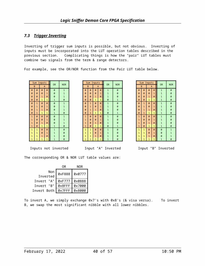
7.3 Trigger Inverting
Inverting of trigger sum inputs is possible, but not obvious. Inverting of inputs must be incorporated into the LUT operation tables described in the previous section. Complicating things is how the "pair" LUT tables must combine two signals from the term & range detectors.
For example, see the OR/NOR function from the Pair LUT table below.
Sum Inputs OR NORB A0 0 0 0 0 10 0 0 1 0 10 0 1 0 0 10 0 1 1 1 00 1 0 0 0 10 1 0 1 0 10 1 1 0 0 10 1 1 1 1 01 0 0 0 0 11 0 0 1 0 11 0 1 0 0 11 0 1 1 1 01 1 0 0 1 01 1 0 1 1 01 1 1 0 1 01 1 1 1 1 0
Inputs not inverted
Sum Inputs OR NORB A0 0 0 0 1 00 0 0 1 1 00 0 1 0 1 00 0 1 1 0 10 1 0 0 1 00 1 0 1 1 00 1 1 0 1 00 1 1 1 0 11 0 0 0 1 01 0 0 1 1 01 0 1 0 1 01 0 1 1 0 11 1 0 0 1 01 1 0 1 1 01 1 1 0 1 01 1 1 1 1 0
Input "A" Inverted
Sum Inputs OR NORB A0 0 0 0 1 00 0 0 1 1 00 0 1 0 1 00 0 1 1 1 00 1 0 0 1 00 1 0 1 1 00 1 1 0 1 00 1 1 1 1 01 0 0 0 1 01 0 0 1 1 01 0 1 0 1 01 0 1 1 1 01 1 0 0 0 11 1 0 1 0 11 1 1 0 0 11 1 1 1 1 0
Input "B" Inverted
The corresponding OR & NOR LUT table values are:
OR NORNon Inverted 0xF88
80x077
7Invert "A" 0xF77
70x088
8Invert "B" 0x8FFF 0x700
0Invert Both 0x7FFF 0x800
0
To invert A, we simply exchange 0x7's with 0x8's (& visa versa). To invert B, we swap the most significant nibble with all lower nibbles.
May 12, 2023 27 of 42 2:51 AM

Logic Sniffer Demon Core FPGA Specification
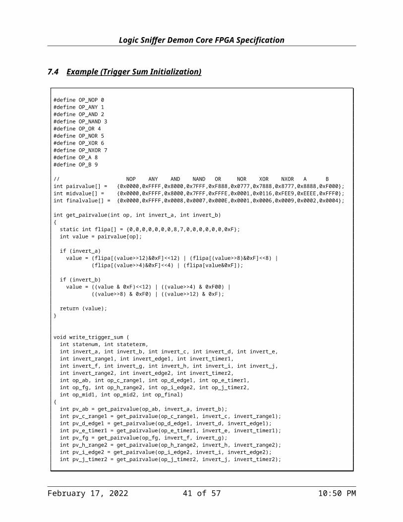
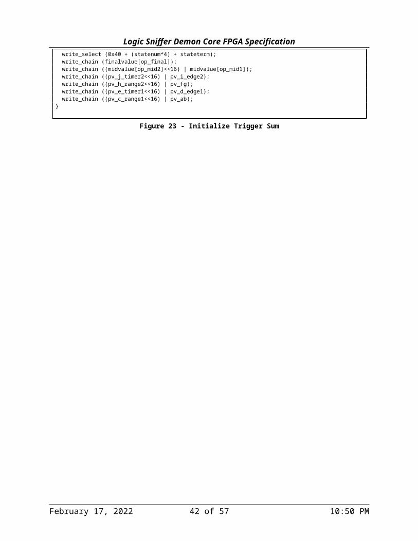
7.4 Example (Trigger Sum Initialization)
#define OP_NOP 0#define OP_ANY 1#define OP_AND 2#define OP_NAND 3#define OP_OR 4#define OP_NOR 5#define OP_XOR 6#define OP_NXOR 7#define OP_A 8#define OP_B 9
// NOP ANY AND NAND OR NOR XOR NXOR A Bint pairvalue[] = {0x0000,0xFFFF,0x8000,0x7FFF,0xF888,0x0777,0x7888,0x8777,0x8888,0xF000};int midvalue[] = {0x0000,0xFFFF,0x8000,0x7FFF,0xFFFE,0x0001,0x0116,0xFEE9,0xEEEE,0xFFF0};int finalvalue[] = {0x0000,0xFFFF,0x0008,0x0007,0x000E,0x0001,0x0006,0x0009,0x0002,0x0004};
int get_pairvalue(int op, int invert_a, int invert_b){ static int flipa[] = {0,0,0,0,0,0,0,8,7,0,0,0,0,0,0,0xF}; int value = pairvalue[op];
if (invert_a) value = (flipa[(value>>12)&0xF]<<12) | (flipa[(value>>8)&0xF]<<8) | (flipa[(value>>4)&0xF]<<4) | (flipa[value&0xF]);
if (invert_b) value = ((value & 0xF)<<12) | ((value>>4) & 0xF00) | ((value>>8) & 0xF0) | ((value>>12) & 0xF);
return (value);}
void write_trigger_sum ( int statenum, int stateterm, int invert_a, int invert_b, int invert_c, int invert_d, int invert_e, int invert_range1, int invert_edge1, int invert_timer1, int invert_f, int invert_g, int invert_h, int invert_i, int invert_j, int invert_range2, int invert_edge2, int invert_timer2, int op_ab, int op_c_range1, int op_d_edge1, int op_e_timer1, int op_fg, int op_h_range2, int op_i_edge2, int op_j_timer2, int op_mid1, int op_mid2, int op_final){ int pv_ab = get_pairvalue(op_ab, invert_a, invert_b); int pv_c_range1 = get_pairvalue(op_c_range1, invert_c, invert_range1); int pv_d_edge1 = get_pairvalue(op_d_edge1, invert_d, invert_edge1); int pv_e_timer1 = get_pairvalue(op_e_timer1, invert_e, invert_timer1); int pv_fg = get_pairvalue(op_fg, invert_f, invert_g); int pv_h_range2 = get_pairvalue(op_h_range2, invert_h, invert_range2); int pv_i_edge2 = get_pairvalue(op_i_edge2, invert_i, invert_edge2); int pv_j_timer2 = get_pairvalue(op_j_timer2, invert_j, invert_timer2);
write_select (0x40 + (statenum*4) + stateterm); write_chain (finalvalue[op_final]); write_chain ((midvalue[op_mid2]<<16) | midvalue[op_mid1]); write_chain ((pv_j_timer2<<16) | pv_i_edge2); write_chain ((pv_h_range2<<16) | pv_fg); write_chain ((pv_e_timer1<<16) | pv_d_edge1); write_chain ((pv_c_range1<<16) | pv_ab); }
May 12, 2023 28 of 42 2:51 AM

Logic Sniffer Demon Core FPGA SpecificationFigure 23 - Initialize Trigger Sum
May 12, 2023 29 of 42 2:51 AM

Logic Sniffer Demon Core FPGA Specification
8 Trigger Sequence States Sequence states allow you to control how the analyzer evaluates and stores sampled data. Each state gives you control over data capturing, searching for a target (optionally multiple times), or branching to another sequence should a special condition occur. On a hit, the analyzer advances to the next sequence state. It can also trigger the analyzer controller & start/stop timers. With 16 sequence states, you can create complex protocol following triggers.
Figure 24 - Example Sequence Level
For each state you specify:
Capture Term (sum of trigger terms, range checks, edge detect & timer hits) Hit Term (sum of trigger terms, range checks, edge detect & timer hits) Else Term (sum of trigger terms, range checks, edge detect & timer hits) Occurrence Count Else State Timer Control Flags (start/stop/clear for timers 1 & 2) Trigger Flag
The trigger sequencer itself is a relatively simple state machine. Pseudocode for it is:
if (sampled_input valid) then {if (capture_term valid) then
capture dataif (hit_term valid) then {
increment hit_countif (hit_count == fsm_occurence_count) then {
update_timersreset hit_countif (fsm_trigger || last_state) then assert run to controllerif (!last_state && !fsm_last_state) advance to next state
}}otherwise if (else_term valid) then {
reset hit_countgo to state "fsm_else_level"
}}
May 12, 2023 30 of 42 2:51 AM
Logic Sniffer Demon Core FPGA Specification
Figure 25 - Trigger Sequencer State Machine
May 12, 2023 31 of 42 2:51 AM

Logic Sniffer Demon Core FPGA Specification
8.1 Example (Trigger Sequence Initialization)
#define TRIGSTATE_STATENUM_MASK 0xF#define TRIGSTATE_OBTAIN_MASK 0x000FFFFF#define TRIGSTATE_ELSE_BITOFS 20#define TRIGSTATE_STOP_TIMER0 0x01000000#define TRIGSTATE_STOP_TIMER1 0x02000000#define TRIGSTATE_CLEAR_TIMER0 0x04000000#define TRIGSTATE_CLEAR_TIMER1 0x08000000#define TRIGSTATE_START_TIMER0 0x10000000#define TRIGSTATE_START_TIMER1 0x20000000#define TRIGSTATE_TRIGGER_FLAG 0x40000000#define TRIGSTATE_LASTSTATE 0x80000000
void write_trigger_state ( int statenum, // 0 to 15 int last_state, int set_trigger, int start_timer, // bit0=timer1, bit1=timer2 int stop_timer, // bit0=timer1, bit1=timer2 int clear_timer, // bit0=timer1, bit1=timer2 int else_state, // 0 to 15 int obtain_count){ write_select (statenum & TRIGSTATE_STATENUM_MASK);
unsigned int value = ((else_state & TRIGSTATE_STATENUM_MASK)<<TRIGSTATE_ELSE_BITOFS) | (obtain_count & TRIGSTATE_OBTAIN_MASK); if (last_state) value |= TRIGGER_LASTSTATE; if (set_trigger) value |= TRIGSTATE_TRIGGER_FLAG; if (start_timer & 1) value |= TRIGSTATE_START_TIMER0; if (start_timer & 2) value |= TRIGSTATE_START_TIMER1; if (stop_timer & 1) value |= TRIGSTATE_STOP_TIMER0; if (stop_timer & 2) value |= TRIGSTATE_STOP_TIMER1; if (clear_timer & 1) value |= TRIGSTATE_CLEAR_TIMER0; if (clear_timer & 2) value |= TRIGSTATE_CLEAR_TIMER1; write_chain (value);}
Figure 26 - Initialize Trigger Sequence
May 12, 2023 32 of 42 2:51 AM
Logic Sniffer Demon Core FPGA Specification
Appendix A - Advanced Trigger Config Registers
The client initializes advanced trigger LUT chains using the 0x9E configuration-select command, followed by one or more 0x9F write-data commands. Each data write adds 32-bits to the selected LUT chain.
Exceptions are the FSM state configs & timer limits, which store DWORD values directly. However, the client sees no difference (just more writes to trigger config regs).
Client Long Commands (command byte + four data bytes, LSB data byte first): 0x9E = ADVTRIG-Config-Select (LSB = Chain#. Other bytes reserved.) 0x9F = ADVTRIG-Write-Data
FSM State Data 0x00 = FSM State 0 (32-bit word's) 0x01 = FSM State 1 0x02 = FSM State 2 0x03 = FSM State 3 0x04 = FSM State 4 0x05 = FSM State 5 0x06 = FSM State 6 0x07 = FSM State 7 0x08 = FSM State 8 0x09 = FSM State 9 0x0A = FSM State 10 0x0B = FSM State 11 0x0C = FSM State 12 0x0D = FSM State 13 0x0E = FSM State 14 0x0F = FSM State 15
LUTCHAIN's: 0x20 = trigger term a (128 bit chains) 0x21 = trigger term b 0x22 = trigger term c 0x23 = trigger term d 0x24 = trigger term e 0x25 = trigger term f 0x26 = trigger term g 0x27 = trigger term h 0x28 = trigger term i 0x29 = trigger term j 0x30 = range 1 lower (512 bit chains) 0x31 = range 1 upper (512 bit chains) 0x32 = range 2 lower (512 bit chains) 0x33 = range 2 upper (512 bit chains) 0x34 = edge 1 (64 bit chains) 0x35 = edge 2 (64 bit chains) 0x38-0x39 = timer 1 limit (36-bit word's) 0x3A-0x3B = timer 2 limit (36-bit word's)
0x40 = state 0 hit-term 0x41 = state 0 else-term 0x42 = state 0 capture-term 0x44-0x46 = state 1 terms 0x48-0x4A = state 2 terms 0x4C-0x4E = state 3 terms 0x50-0x52 = state 4 terms 0x54-0x56 = state 5 terms 0x58-0x5A = state 6 terms 0x5C-0x5E = state 7 terms 0x60-0x62 = state 8 terms 0x64-0x66 = state 9 terms 0x68-0x6A = state 10 terms 0x6C-0x6E = state 11 terms
May 12, 2023 33 of 42 2:51 AM
Logic Sniffer Demon Core FPGA Specification 0x70-0x72 = state 12 terms 0x74-0x76 = state 13 terms 0x78-0x7A = state 14 terms 0x7C-0x7E = state 15 terms
May 12, 2023 34 of 42 2:51 AM
Logic Sniffer Demon Core FPGA Specification
Appendix B - Example Code
#define write_select(value) write_long_command (0x9E, value)#define write_chain(value) write_long_command (0x9F, value)
#define RANGE_XOR0 0xAAAA#define RANGE_XOR1 0x5555#define RANGE_NOP 0xFFFF
#define EDGE_RISE0 0x0A0A#define EDGE_RISE1 0x00CC#define EDGE_FALL0 0x5050#define EDGE_FALL1 0x3300#define EDGE_BOTH0 (EDGE_RISE0|EDGE_FALL0)#define EDGE_BOTH1 (EDGE_RISE1|EDGE_FALL1)#define EDGE_NEITHER0 (~EDGE_BOTH0 & 0xFFFF)#define EDGE_NEITHER1 (~EDGE_BOTH1 & 0xFFFF)
#define TRIGSTATE_STATENUM_MASK 0xF#define TRIGSTATE_OBTAIN_MASK 0x000FFFFF#define TRIGSTATE_ELSE_BITOFS 20#define TRIGSTATE_STOP_TIMER0 0x01000000#define TRIGSTATE_STOP_TIMER1 0x02000000#define TRIGSTATE_CLEAR_TIMER0 0x04000000#define TRIGSTATE_CLEAR_TIMER1 0x08000000#define TRIGSTATE_START_TIMER0 0x10000000#define TRIGSTATE_START_TIMER1 0x20000000#define TRIGSTATE_TRIGGER_FLAG 0x40000000#define TRIGSTATE_LASTSTATE 0x80000000
#define OP_NOP 0#define OP_ANY 1#define OP_AND 2#define OP_NAND 3#define OP_OR 4#define OP_NOR 5#define OP_XOR 6#define OP_NXOR 7#define OP_A 8#define OP_B 9
//// Setup LUT's for Trigger Term// // Inputs are 32-bit target & mask for comparing against captured analyzer data.// If a mask bit is set, the corresponding target bit participates in the trigger.//void write_term (int term_number, unsigned int target, unsigned int mask){ unsigned int bitmask=1; unsigned int lutvalue0=0; unsigned int lutvalue1=0; unsigned int lutvalue2=0; unsigned int lutvalue3=0;
for (int i=0; i<16; i=i+1) { if (((i ^ (target & 0xF)) & (mask & 0xF))==0) lutvalue0 |= bitmask; if (((i ^ ((target>>4) & 0xF)) & ((mask>>4) & 0xF))==0) lutvalue0 |= (bitmask<<16); if (((i ^ ((target>>8) & 0xF)) & ((mask>>8) & 0xF))==0) lutvalue1 |= bitmask; if (((i ^ ((target>>12) & 0xF)) & ((mask>>12) & 0xF))==0) lutvalue1 |= (bitmask<<16); if (((i ^ ((target>>16) & 0xF)) & ((mask>>16) & 0xF))==0) lutvalue2 |= bitmask; if (((i ^ ((target>>20) & 0xF)) & ((mask>>20) & 0xF))==0) lutvalue2 |= (bitmask<<16); if (((i ^ ((target>>24) & 0xF)) & ((mask>>24) & 0xF))==0) lutvalue3 |= bitmask; if (((i ^ ((target>>28) & 0xF)) & ((mask>>28) & 0xF))==0) lutvalue3 |= (bitmask<<16); bitmask <<= 1; }
May 12, 2023 35 of 42 2:51 AM
Logic Sniffer Demon Core FPGA Specification
// Write data into LUT serial chain. MSB must goes in first. Total of 128 bits. write_select (0x20 + (term_number%10)); write_chain (lutvalue3); write_chain (lutvalue2); write_chain (lutvalue1); write_chain (lutvalue0);}
//// Setup LUT's for Range Detectors//// Inputs:// rangesel: 0=range1-lower, 1=range1-upper, 2=range2-lower, 3=range2-upper// target: Limit value.// mask: Indicate which bits should participate in range compare. //void write_range (int rangesel, unsigned int target, unsigned int mask){ unsigned int value; unsigned int lutvalue=0; int i;
write_select(0x30+(rangesel&3));
// Count # of bits in mask... int bitcount=0; unsigned int bitmask=1; for (i=0; i<32; i++, bitmask<<=1) if (mask & bitmask) bitcount++;
// Prepare target value... if (rangesel & 1) value = ~target; // upper range target else value = ~(target-1); // lower range value
// Push MSB of target into bit 31... value <<= (32-bitcount);
// Generate & program LUT values. Total of 512 bits. for (i=0; i<16; i=i+1) { if (((mask>>31)&1)==0) lutvalue = RANGE_NOP; else { lutvalue = ((value>>31)&1) ? RANGE_XOR1 : RANGE_XOR0; value <<= 1; } mask <<= 1; lutvalue <<= 16;
if (((mask>>31)&1)==0) lutvalue |= RANGE_NOP; else { lutvalue |= ((value>>31)&1) ? RANGE_XOR1 : RANGE_XOR0; value <<= 1; } mask <<= 1;
write_chain(lutvalue); }}
//// Setup LUT's for Edge Detectors.// Each LUT handles two bits of input. Bits 0 & 1 are input. Bits 2 & 3 delayed input.//
May 12, 2023 36 of 42 2:51 AM

Logic Sniffer Demon Core FPGA Specificationvoid write_edge (int edgesel, unsigned int rising_edge, unsigned int falling_edge, unsigned int neither_edge){ write_select (0x34 + (edgesel&1));
unsigned int lutvalue=0; unsigned int bitmask = 0x80000000; for (int i=0; i<16; i=i+1) { // Evaluate indata bit1... if (neither_edge && bitmask) lutvalue |= EDGE_NEITHER1; else { if (rising_edge & bitmask) lutvalue |= EDGE_RISE1; if (falling_edge & bitmask) lutvalue |= EDGE_FALL1; } bitmask >>= 1;
// Evaluate indata bit0... if (neither_edge && bitmask) lutvalue |= EDGE_NEITHER0; else { if (rising_edge & bitmask) lutvalue |= EDGE_RISE0; if (falling_edge & bitmask) lutvalue |= EDGE_FALL0; } bitmask >>= 1;
if ((i&1)==0) lutvalue <<= 16; else { write_chain (lutvalue); // write total of 256 bits lutvalue = 0; } }}
//// Setup trigger timers...//void write_trigger_limit (int timersel, uint64_t value){ write_select (0x38 + (timersel&1)*2); write_chain (value & 0xFFFFFFFF); write_select (0x39 + (timersel&1)*2); write_chain (value>>32);}
//// Setup trigger state term combinational sum. Operations for// all 11 fields are merged & written. Uses table based lookups.//// NOP ANY AND NAND OR NOR XOR NXOR A Bint pairvalue[] = {0x0000,0xFFFF,0x8000,0x7FFF,0xF888,0x0777,0x7888,0x8777,0x8888,0xF000};int midvalue[] = {0x0000,0xFFFF,0x8000,0x7FFF,0xFFFE,0x0001,0x0116,0xFEE9,0xEEEE,0xFFF0};int finalvalue[] = {0x0000,0xFFFF,0x0008,0x0007,0x000E,0x0001,0x0006,0x0009,0x0002,0x0004};
int get_pairvalue(int op, int invert_a, int invert_b){ static int flipa[] = {0,0,0,0,0,0,0,8,7,0,0,0,0,0,0,0xF}; int value = pairvalue[op];
if (invert_a) value = (flipa[(value>>12)&0xF]<<12) | (flipa[(value>>8)&0xF]<<8) | (flipa[(value>>4)&0xF]<<4) | (flipa[value&0xF]);
if (invert_b) value = ((value & 0xF)<<12) | ((value>>4) & 0xF00) | ((value>>8) & 0xF0) | ((value>>12) & 0xF);
May 12, 2023 37 of 42 2:51 AM
Logic Sniffer Demon Core FPGA Specification
return (value);}
void write_trigger_sum ( int statenum, int stateterm, int invert_a, int invert_b, int invert_c, int invert_d, int invert_e, int invert_range1, int invert_edge1, int invert_timer1, int invert_f, int invert_g, int invert_h, int invert_i, int invert_j, int invert_range2, int invert_edge2, int invert_timer2, int op_ab, int op_c_range1, int op_d_edge1, int op_e_timer1, int op_fg, int op_h_range2, int op_i_edge2, int op_j_timer2, int op_mid1, int op_mid2, int op_final){ int pv_ab = get_pairvalue(op_ab, invert_a, invert_b); int pv_c_range1 = get_pairvalue(op_c_range1, invert_c, invert_range1); int pv_d_edge1 = get_pairvalue(op_d_edge1, invert_d, invert_edge1); int pv_e_timer1 = get_pairvalue(op_e_timer1, invert_e, invert_timer1); int pv_fg = get_pairvalue(op_fg, invert_f, invert_g); int pv_h_range2 = get_pairvalue(op_h_range2, invert_h, invert_range2); int pv_i_edge2 = get_pairvalue(op_i_edge2, invert_i, invert_edge2); int pv_j_timer2 = get_pairvalue(op_j_timer2, invert_j, invert_timer2);
write_select (0x40 + (statenum*4) + stateterm); write_chain (finalvalue[op_final]); write_chain ((midvalue[op_mid2]<<16) | midvalue[op_mid1]); write_chain ((pv_j_timer2<<16) | pv_i_edge2); write_chain ((pv_h_range2<<16) | pv_fg); write_chain ((pv_e_timer1<<16) | pv_d_edge1); write_chain ((pv_c_range1<<16) | pv_ab); }
May 12, 2023 38 of 42 2:51 AM
Logic Sniffer Demon Core FPGA Specification
//// Setup trigger state. Specify trigger mode, timer controls, "else" state number,// and necessary "obtain" count (number of hits needed before full hit observed).//void write_trigger_state ( int statenum, // 0 to 15 int last_state, int set_trigger, int start_timer, // bit0=timer1, bit1=timer2 int stop_timer, // bit0=timer1, bit1=timer2 int clear_timer, // bit0=timer1, bit1=timer2 int else_state, // 0 to 15 int obtain_count){ write_select (statenum & TRIGSTATE_STATENUM_MASK);
unsigned int value = ((else_state & TRIGSTATE_STATENUM_MASK)<<TRIGSTATE_ELSE_BITOFS) | (obtain_count & TRIGSTATE_OBTAIN_MASK); if (last_state) value |= TRIGSTATE_LASTSTATE; if (set_trigger) value |= TRIGSTATE_TRIGGER_FLAG; if (start_timer & 1) value |= TRIGSTATE_START_TIMER0; if (start_timer & 2) value |= TRIGSTATE_START_TIMER1; if (stop_timer & 1) value |= TRIGSTATE_STOP_TIMER0; if (stop_timer & 2) value |= TRIGSTATE_STOP_TIMER1; if (clear_timer & 1) value |= TRIGSTATE_CLEAR_TIMER0; if (clear_timer & 2) value |= TRIGSTATE_CLEAR_TIMER1; write_chain (value);}
May 12, 2023 39 of 42 2:51 AM
Logic Sniffer Demon Core FPGA Specification
GNU GENERAL PUBLIC LICENSEVersion 2, June 1991
Copyright (C) 1989, 1991 Free Software Foundation, Inc. 51 Franklin Street, Fifth Floor, Boston, MA 02110-1301 USAEveryone is permitted to copy and distribute verbatim copies of this license document, but changing it is not allowed.
Preamble
The licenses for most software are designed to take away your freedom to share and change it. By contrast, the GNU General Public License is intended to guarantee your freedom to share and change free software--to make sure the software is free for all its users. This General Public License applies to most of the Free Software Foundation's software and to any other program whose authors commit to using it. (Some other Free Software Foundation software is covered by the GNU Lesser General Public License instead.) You can apply it to your programs, too.
When we speak of free software, we are referring to freedom, not price. Our General Public Licenses are designed to make sure that you have the freedom to distribute copies of free software (and charge for this service if you wish), that you receive source code or can get it if you want it, that you can change the software or use pieces of it in new free programs; and that you know you can do these things.
To protect your rights, we need to make restrictions that forbid anyone to deny you these rights or to ask you to surrender the rights. These restrictions translate to certain responsibilities for you if you distribute copies of the software, or if you modify it.
For example, if you distribute copies of such a program, whether gratis or for a fee, you must give the recipients all the rights that you have. You must make sure that they, too, receive or can get the source code. And you must show them these terms so they know theirrights.
We protect your rights with two steps: (1) copyright the software, and (2) offer you this license which gives you legal permission to copy, distribute and/or modify the software.
Also, for each author's protection and ours, we want to make certain that everyone understands that there is no warranty for this free software. If the software is modified by someone else and passed on, we want its recipients to know that what they have is not the original, so that any problems introduced by others will not reflect on the original authors' reputations.
Finally, any free program is threatened constantly by software patents. We wish to avoid the danger that redistributors of a free program will individually obtain patent licenses, in effect making the program proprietary. To prevent this, we have made it clear that any patent must be licensed for everyone's free use or not licensed at all.
The precise terms and conditions for copying, distribution and modification follow.
GNU GENERAL PUBLIC LICENSETERMS AND CONDITIONS FOR COPYING, DISTRIBUTION AND MODIFICATION
0. This License applies to any program or other work which contains a notice placed by the copyright holder saying it may be distributed under the terms of this General Public License. The "Program", below, refers to any such program or work, and a "work based on the Program" means either the Program or any derivative work under copyright law: that is to say, a work containing the Program or a portion of it, either verbatim or with modifications and/or translated into another language. (Hereinafter, translation is included without limitation in the term "modification".) Each licensee is addressed as "you".
Activities other than copying, distribution and modification are not covered by this License; they are outside its scope. The act of running the Program is not restricted, and the output from the Program is covered only if its contents constitute a work based on the Program (independent of having been made by running the Program). Whether that is true depends on what the Program does.
1. You may copy and distribute verbatim copies of the Program's source code as you receive it, in any medium, provided that you conspicuously and appropriately publish on each copy an appropriate copyright notice and disclaimer of warranty; keep intact all the notices that refer to this License and to the absence of any warranty; and give any other recipients of the Program a copy of this License along with the Program.
You may charge a fee for the physical act of transferring a copy, and you may at your option offer warranty protection in exchange for a fee.
2. You may modify your copy or copies of the Program or any portion of it, thus forming a work based on the Program, and copy and distribute such modifications or work under the terms of Section 1above, provided that you also meet all of these conditions:
a) You must cause the modified files to carry prominent notices stating that you changed the files and the date of any change.
b) You must cause any work that you distribute or publish, that in whole or in part contains or is derived from the Program or any part thereof, to be licensed as a whole at no charge to all third parties under the terms of this License.
May 12, 2023 40 of 42 2:51 AM
Logic Sniffer Demon Core FPGA Specification c) If the modified program normally reads commands interactively when run, you must cause it, when started running for such interactive use in the most ordinary way, to print or display an announcement including an appropriate copyright notice and a notice that there is no warranty (or else, saying that you provide a warranty) and that users may redistribute the program under these conditions, and telling the user how to view a copy of this License. (Exception: if the Program itself is interactive but does not normally print such an announcement, your work based on the Program is not required to print an announcement.)
These requirements apply to the modified work as a whole. If identifiable sections of that work are not derived from the Program,and can be reasonably considered independent and separate works in themselves, then this License, and its terms, do not apply to thosesections when you distribute them as separate works. But when you distribute the same sections as part of a whole which is a work basedon the Program, the distribution of the whole must be on the terms of this License, whose permissions for other licensees extend to theentire whole, and thus to each and every part regardless of who wrote it.
Thus, it is not the intent of this section to claim rights or contest your rights to work written entirely by you; rather, the intent is toexercise the right to control the distribution of derivative or collective works based on the Program.
In addition, mere aggregation of another work not based on the Program with the Program (or with a work based on the Program) on a volume ofa storage or distribution medium does not bring the other work under the scope of this License.
3. You may copy and distribute the Program (or a work based on it, under Section 2) in object code or executable form under the terms ofSections 1 and 2 above provided that you also do one of the following:
a) Accompany it with the complete corresponding machine-readable source code, which must be distributed under the terms of Sections 1 and 2 above on a medium customarily used for software interchange; or,
b) Accompany it with a written offer, valid for at least three years, to give any third party, for a charge no more than your cost of physically performing source distribution, a complete machine-readable copy of the corresponding source code, to be distributed under the terms of Sections 1 and 2 above on a medium customarily used for software interchange; or,
c) Accompany it with the information you received as to the offer to distribute corresponding source code. (This alternative is allowed only for noncommercial distribution and only if you received the program in object code or executable form with such an offer, in accord with Subsection b above.)
The source code for a work means the preferred form of the work for making modifications to it. For an executable work, complete source code means all the source code for all modules it contains, plus any associated interface definition files, plus the scripts used to control compilation and installation of the executable. However, as a special exception, the source code distributed need not include anything that is normally distributed (in either source or binary form) with the major components (compiler, kernel, and so on) of the operating system on which the executable runs, unless that component itself accompanies the executable.
If distribution of executable or object code is made by offering access to copy from a designated place, then offering equivalent access to copy the source code from the same place counts as distribution of the source code, even though third parties are not compelled to copy the source along with the object code.
4. You may not copy, modify, sublicense, or distribute the Program except as expressly provided under this License. Any attempt otherwise to copy, modify, sublicense or distribute the Program is void, and will automatically terminate your rights under this License. However, parties who have received copies, or rights, from you under this License will not have their licenses terminated so long as such parties remain in full compliance.
5. You are not required to accept this License, since you have not signed it. However, nothing else grants you permission to modify or distribute the Program or its derivative works. These actions are prohibited by law if you do not accept this License. Therefore, by modifying or distributing the Program (or any work based on the Program), you indicate your acceptance of this License to do so, and all its terms and conditions for copying, distributing or modifying the Program or works based on it.
6. Each time you redistribute the Program (or any work based on the Program), the recipient automatically receives a license from the original licensor to copy, distribute or modify the Program subject to these terms and conditions. You may not impose any further restrictions on the recipients' exercise of the rights granted herein. You are not responsible for enforcing compliance by third parties to this License.
7. If, as a consequence of a court judgment or allegation of patent infringement or for any other reason (not limited to patent issues), conditions are imposed on you (whether by court order, agreement or otherwise) that contradict the conditions of this License, they do not excuse you from the conditions of this License. If you cannot distribute so as to satisfy simultaneously your obligations under this License and any other pertinent obligations, then as a consequence you may not distribute the Program at all. For example, if a patent license would not permit royalty-free redistribution of the Program by all those who receive copies directly or indirectly through you, then the only way you could satisfy both it and this License would be to refrain entirely from distribution of the Program.
If any portion of this section is held invalid or unenforceable under any particular circumstance, the balance of the section is intended to apply and the section as a whole is intended to apply in other circumstances.
It is not the purpose of this section to induce you to infringe any patents or other property right claims or to contest validity of any such claims; this section has the sole purpose of protecting the integrity of the free software distribution system, which is implemented by public license practices. Many people have made generous contributions to the wide range of software distributed through that system in reliance on consistent
May 12, 2023 41 of 42 2:51 AM
Logic Sniffer Demon Core FPGA Specificationapplication of that system; it is up to the author/donor to decide if he or she is willing to distribute software through any other system and a licensee cannot impose that choice.
This section is intended to make thoroughly clear what is believed to be a consequence of the rest of this License. 8. If the distribution and/or use of the Program is restricted in certain countries either by patents or by copyrighted interfaces, the original copyright holder who places the Program under this License may add an explicit geographical distribution limitation excluding those countries, so that distribution is permitted only in or among countries not thus excluded. In such case, this License incorporates the limitation as if written in the body of this License.
9. The Free Software Foundation may publish revised and/or new versions of the General Public License from time to time. Such new versions will be similar in spirit to the present version, but may differ in detail to address new problems or concerns.
Each version is given a distinguishing version number. If the Program specifies a version number of this License which applies to it and "any later version", you have the option of following the terms and conditions either of that version or of any later version published by the Free Software Foundation. If the Program does not specify a version number of this License, you may choose any version ever published by the Free Software Foundation.
10. If you wish to incorporate parts of the Program into other free programs whose distribution conditions are different, write to the author to ask for permission. For software which is copyrighted by the Free Software Foundation, write to the Free Software Foundation; we sometimes make exceptions for this. Our decision will be guided by the two goals of preserving the free status of all derivatives of our free software and of promoting the sharing and reuse of software generally.
NO WARRANTY
11. BECAUSE THE PROGRAM IS LICENSED FREE OF CHARGE, THERE IS NO WARRANTY FOR THE PROGRAM, TO THE EXTENT PERMITTED BY APPLICABLE LAW. EXCEPT WHEN OTHERWISE STATED IN WRITING THE COPYRIGHT HOLDERS AND/OR OTHER PARTIES PROVIDE THE PROGRAM "AS IS" WITHOUT WARRANTY OF ANY KIND, EITHER EXPRESSED OR IMPLIED, INCLUDING, BUT NOT LIMITED TO, THE IMPLIED WARRANTIES OF MERCHANTABILITY AND FITNESS FOR A PARTICULAR PURPOSE. THE ENTIRE RISK AS TO THE QUALITY AND PERFORMANCE OF THE PROGRAM IS WITH YOU. SHOULD THE PROGRAM PROVE DEFECTIVE, YOU ASSUME THE COST OF ALL NECESSARY SERVICING, REPAIR OR CORRECTION.
12. IN NO EVENT UNLESS REQUIRED BY APPLICABLE LAW OR AGREED TO IN WRITING WILL ANY COPYRIGHT HOLDER, OR ANY OTHER PARTY WHO MAY MODIFY AND/OR REDISTRIBUTE THE PROGRAM AS PERMITTED ABOVE, BE LIABLE TO YOU FOR DAMAGES, INCLUDING ANY GENERAL, SPECIAL, INCIDENTAL OR CONSEQUENTIAL DAMAGES ARISINGOUT OF THE USE OR INABILITY TO USE THE PROGRAM (INCLUDING BUT NOT LIMITED TO LOSS OF DATA OR DATA BEING RENDERED INACCURATE OR LOSSES SUSTAINED BY YOU OR THIRD PARTIES OR A FAILURE OF THE PROGRAM TO OPERATE WITH ANY OTHER PROGRAMS), EVEN IF SUCH HOLDER OR OTHER PARTY HAS BEEN ADVISED OF THEPOSSIBILITY OF SUCH DAMAGES.
END OF TERMS AND CONDITIONS
May 12, 2023 42 of 42 2:51 AM